High Performance ISM Band
ASK/FSK/GFSK Transmitter IC
ADF7011
FEATURES
Single Chip Low Power UHF Transmitter
Frequency Band
433 MHz to 435 MHz
868 MHz to 870 MHz
On-Chip VCO and Fractional-N PLL
2.3 V to 3.6 V Supply Voltage
Programmable Output Power
–16 dBm to +12 dBm, 0.3 dB Steps
Data Rates up to 76.8 kbps
Low Current Consumption
29 mA at +10 dBm at 433.92 MHz
Power-Down Mode (<1 A)
24-Lead TSSOP Package Hooks to External VCO for
< 1.4 GHz Operation
APPLICATIONS
Low Cost Wireless Data Transfer
Wireless Metering
Remote Control/Security Systems
Keyless Entry
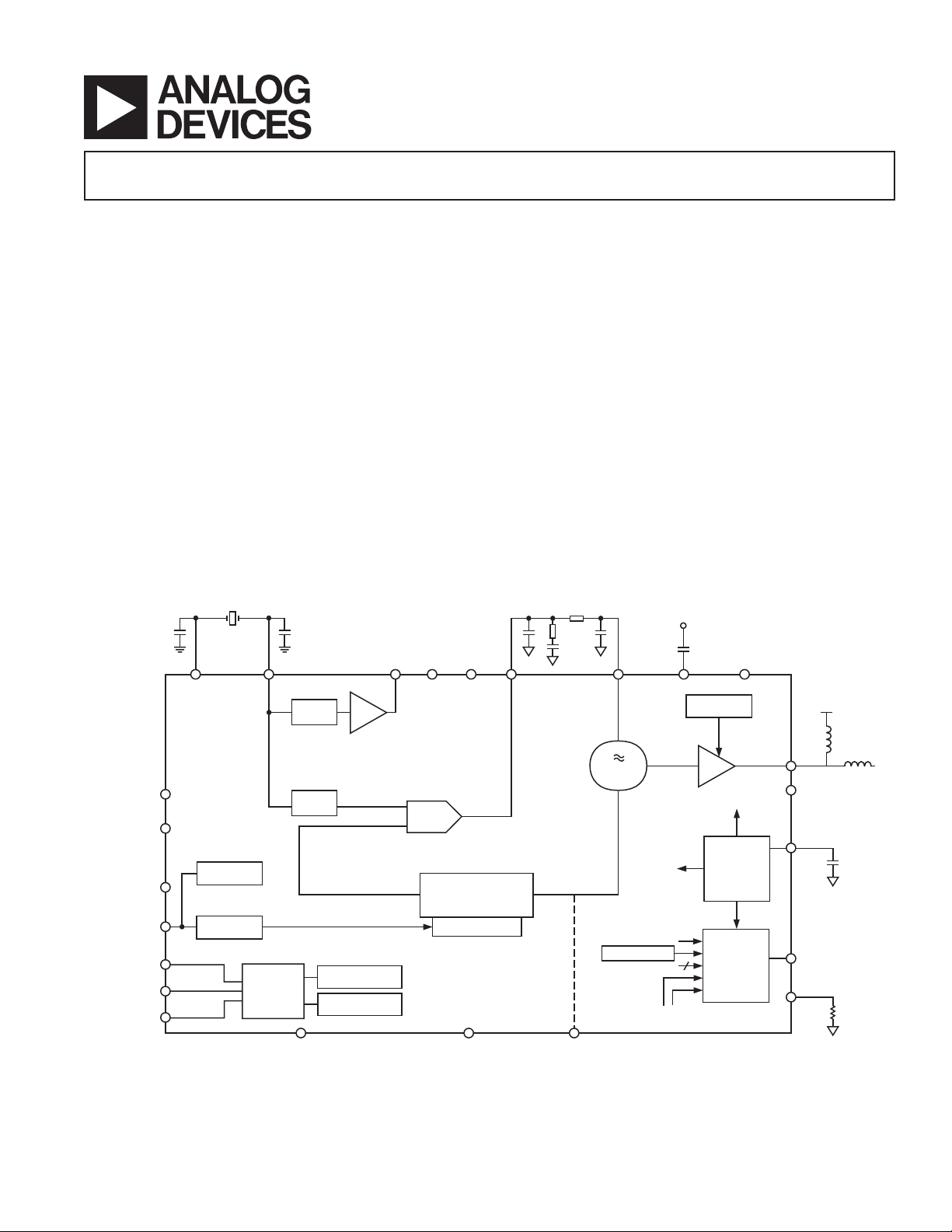
FUNCTIONAL BLOCK DIAGRAM
CPVDDCP
CLK
OSC1
OSC2
CLK
OUT
GENERAL DESCRIPTION
The ADF7011 is a low power OOK/ASK/FSK/GFSK UHF
transmitter designed for use in ISM band systems. It contains
and integrated VCO and Σ-∆ fractional-N PLL. The output
power, channel spacing, and output frequency are programmable with four 24-bit registers. The fractional-N PLL enables
the user to select any channel frequency within the European
433 MHz and 868 MHz bands, allowing the use of the ADF7011
in frequency hopping systems. The fractional-N also allows the
transmitter to operate in the less congested sub-bands of the
868 MHz to 870 MHz SRD band.
It is possible to choose from the four different modulation
schemes: Binary or Gaussian Frequency Shift Keying (FSK/
GFSK), Amplitude Shift Keying (ASK), or On/Off Keying
(OOK). The device also features a crystal compensation register
that can provide ±1 ppm resolution in the output frequency.
Indirect temperature compensation of the crystal can be accomplished inexpensively using this register.
Control of the four on-chip registers is via a simple 3-wire interface. The devices operate with a power supply ranging from
2.3 V to 3.6 V and can be powered down when not in use.
C
REG
VCO
GND
CP
OUT
VCO
C
VCO
IN
OOK/ASK
GND
V
DD
DV
D
GND
TxCLK
TxDATA
DATA
CLK
DD
OOK/ASK
FSK/GFSK
LE
SERIAL
INTERFACE
R
COMPENSATION
CE
FREQUENCY
CENTER
FREQUENCY
PFD/
CHARGE
PUMP
FRACTIONAL-N
SIGMA-DELTA
ADF7011
A
REV. 0
Information furnished by Analog Devices is believed to be accurate and
reliable. However, no responsibility is assumed by Analog Devices for its
use, nor for any infringements of patents or other rights of third parties that
may result from its use. No license is granted by implication or otherwise
under any patent or patent rights of Analog Devices. Trademarks and
registered trademarks are the property of their respective companies.
VCO
LOCK DETECT
GND
One Technology Way, P.O. Box 9106, Norwood, MA 02062-9106, U.S.A.
Tel: 781/329-4700 www.analog.com
Fax: 781/326-8703 © 2003 Analog Devices, Inc. All rights reserved.
TEST
PA
LDO
REGULATOR
MUXOUT
RF
RF
C
MUXOUT
R
OUT
GND
REG
SET

ADF7011–SPECIFICATIONS
(VDD = 2.3 V to 3.6 V, GND = 0 V, TA = T
1
Typical specifications are at VDD = 3 V, TA = 25ⴗC, FPFD = 4 MHz @ 433 MHz,
MIN
to T
FPFD = 22.1184/5.)
Parameter Min Typ Max Unit
RF CHARACTERISTICS
Output Frequency Ranges
Lower SRD Band 433 435 MHz
Upper SRD Band 868 870 MHz
Phase Frequency Detector Frequency 3.4 20 MHz
TRANSMISSION PARAMETERS
Transmit Rate
2
FSK 0.3 76.8 kbits/s
ASK 0.3 9.6 kbits/s
GFSK 0.3 76.8 kbits/s
Frequency Shift Keying
FSK Separation
3
1 110 kHz using 3.625 MHz PFD
4.88 620 kHz using 20 MHz PFD
Gaussian Filter t 0.5
Amplitude Shift Keying Depth 28 dB
On/Off Keying 40 dB
Output Power (No Filtering)
4
868 MHz 3 dBm
433 MHz 10 dBm
Output Power Variation
Max Power Setting 9 12 dBm V
Max Power Setting 11 dBm V
Max Power Setting 9.5 dBm V
Programmable Step Size
–16 dBm to +12 dBm 0.3125 dB
LOGIC INPUTS
V
, Input High Voltage 0.7 V
INH
, Input Low Voltage 0.2 V
V
INL
I
C
, Input Current 1 µA
INH/IINL
, Input Capacitance 10 pF
IN
DD
DD
V
V
Control Clock Input 50 MHz
LOGIC OUTPUTS
VOH, Output High Voltage DV
, Output Low Voltage 0.4 V, I
V
OL
CLK
CLK
Rise/Fall Time 16 ns F
OUT
Mark: Space Ratio 50:50
OUT
– 0.4 V, I
DD
POWER SUPPLIES
Voltage Supply
DV
DD
2.3 3.6 V
Transmit Current Consumption
433 MHz
0 dBm (1 mW) 17 mA
10 dBm (10 mW) 29 mA
868 MHz
0 dBm (1 mW) 19 mA
3 dBm (2 mW) 20.5 mA
10 dBm (10 mW) 34 mA
Crystal Oscillator Block Current
Consumption 190 µA
Regulator Current Consumption 280 µA
Power-Down Mode
Low Power Sleep Mode 0.2 1 µA
, unless otherwise noted.
MAX
= 3.6 V
DD
= 3.0 V
DD
= 2.3 V
DD
= 500 µA
OH
= 500 µA
OL
= 4.8 MHz into 10 pF
CLK
REV. 0–2–

ADF7011
Parameter Min Typ Max Unit
PHASE-LOCKED LOOP
VCO Gain 433 MHz/868 MHz 40/80 MHz/V @ 868 MHz
5
Phase Noise (In-Band)
Phase Noise (Out-of-Band)
Phase Noise (In-Band)7 868 MHz –83 dBc/Hz @ 5 kHz offset
Phase Noise (Out-of-Band)
Spurious
9, 10
47–74, 87.5–118, 174–230, 470–862 MHz –54 dBm
9 kHz – 1 GHz –36 dBm
Above 1 GHz –30 dBm. Assumes external harmonic filter.
Harmonics
10
Second Harmonic, 433 MHz/868 MHz –23/–28 –20/–23 dBc
Third Harmonic, 433 MHz/868 MHz –25/–29 –22/–25 dBc
Other Harmonics, 433 MHz/868 MHz –26/–40 –23/–35 dBc
REFERENCE INPUT
Crystal Reference
433 MHz 1.7 22.1184 MHz
868 MHz 3.4 22.1184 MHz
External Oscillator
Frequency 3.4 40 MHz
Input Level, High Voltage 0.7 V
Input Level, Low Voltage 0.2 V
FREQUENCY COMPENSATION
Pull In Range of Register 1 100 ppm
PA CHARACTERISTICS
RF Output Impedance
868 MHz 16 – j33 , Z
433 MHz 25 – j2.6 , Z
TIMING INFORMATION
Chip Enabled to Regulator Ready
Crystal Oscillator to CLK
4 MHz Crystal 1.8 ms
22.1184 MHz Crystal 2.2 ms
TEMPERATURE RANGE – T
NOTES
1
Operating temperature range is as follows: –40C to +85C.
2
Datarates should be limited to adhere to edge of band requirements in accordance with ETSI 300-220
3
Frequency Deviation = (PFD Frequency Mod Deviation )/212.
GFSK Frequency Deviation = (PFD Frequency 2m)/2
4
The output power is limited by the spurious requirements of ETSI at +55C. The addition of an output filter (see Applications section) will allow increased output
levels to >10 dBm at both 433 MHz and 868 MHz
5
VDD = 3 V, PFD = 4 MHz, PA = 10 dBm
6
VDD = 3 V, Loop Filter BW = 100 kHz
7
VDD = 3 V, PFD = 4.42368 MHz, PA = 3 dBm
8
VDD = 3 V, Loop Filter BW = 100 kHz
9
These spurious levels are based on a maximum output power of +3 dBm for 868 MHz and +10 dBm for 433 MHz. It assumes a PFD frequency of <5 MHz.
Recommended PFD frequencies are 4.42368 MHz (22.1184/5) for 868 MHz, and 4 MHz for 433 MHz operation. Compliance for higher output powers will require
an external filter. See Applications section.
10
Not production tested. Based on characterization.
Specifications subject to change without notice.
433 MHz –81 dBc/Hz @ 5 kHz offset
6
8
–90 dBc/Hz @ 1 MHz offset
–95 dBc/Hz @ 1 MHz offset
100 kHz loop BW
V
V
= 50
REF
= 50
REF
OUT
OK
A
DD
DD
10
50 200 µs
–40 +85 C
12
where m = Mod Control.
REV. 0
–3–
ADF7011
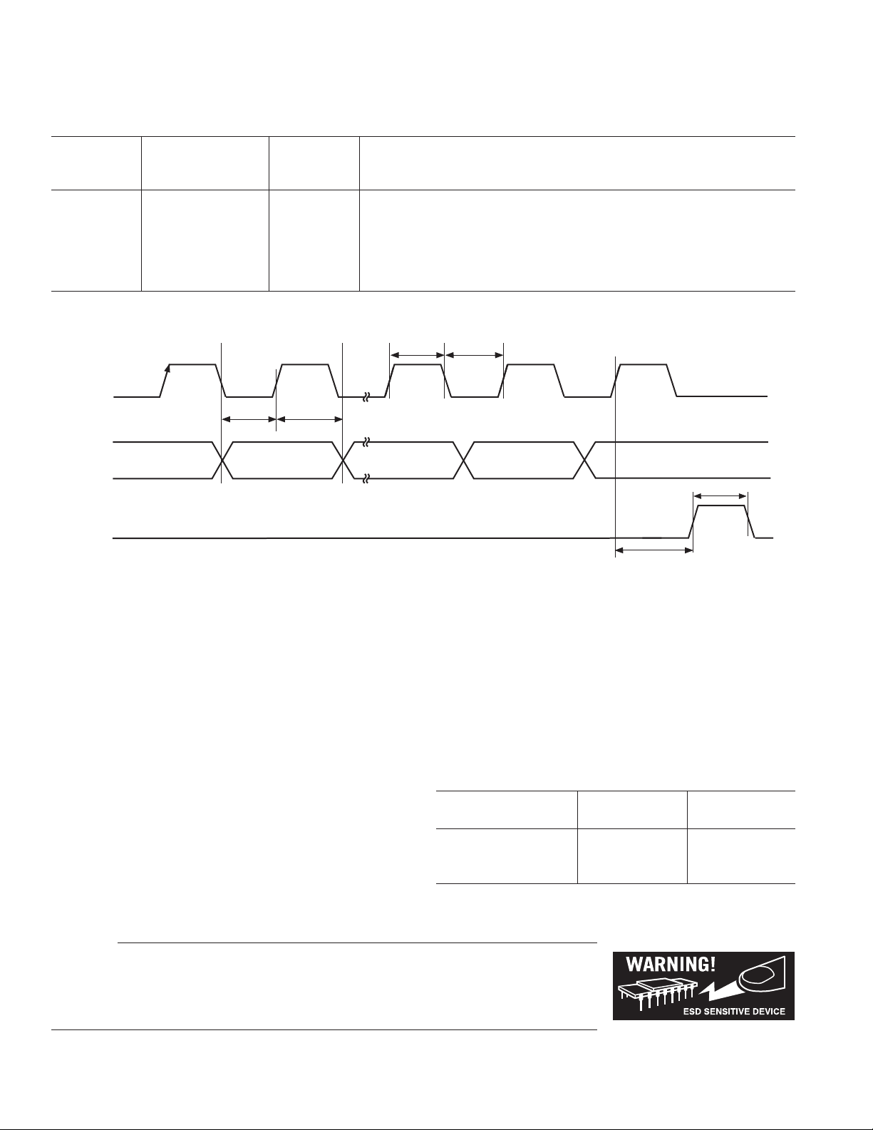
TIMING CHARACTERISTICS
(VDD = 3 V ⴞ 10%; VGND = 0 V, TA = 25ⴗC, unless otherwise noted.)
Limit at
to T
T
MIN
MAX
Parameter (B Version) Unit Test Conditions/Comments
t
1
t
2
t
3
t
4
t
5
t
6
Guaranteed by design but not production tested.
Specifications subject to change without notice.
CLOCK
DATA
LE
10 ns min DATA to CLOCK Setup Time
10 ns min DATA to CLOCK Hold Time
25 ns min CLOCK High Duration
25 ns min CLOCK Low Duration
10 ns min CLOCK to LE Setup Time
20 ns min LE Pulsewidth
t
1
DB23 (MSB) DB22 DB2
t
2
t
3
t
4
(CONTROL BIT C2)
DB1
DB0 (LSB)
(CONTROL BIT C1)
t
6
Figure 1. Timing Diagram
ABSOLUTE MAXIMUM RATINGS
(TA = 25°C, unless otherwise noted.)
1, 2
VDD to GND3 . . . . . . . . . . . . . . . . . . . . . . . . . –0.3 V to + 7 V
to GND . . . . . . . . . . . . . . . . . . . . . . . –0.3 V to + 7 V
CPV
DD
Digital I/O Voltage to GND . . . . . . . –0.3 V to DV
+ 0.3 V
DD
Operating Temperature Range
Industrial (B Version) . . . . . . . . . . . . . . . . –40°C to +85°C
Storage Temperature Range . . . . . . . . . . . . –65°C to +125°C
NOTES
1
Stresses above those listed under Absolute Maximum Ratings may cause permanent damage to the device. This is a stress rating only; functional operation of the
device at these or any other conditions above those listed in the operational
sections of this specification is not implied. Exposure to absolute maximum rating
conditions for extended periods may affect device reliability.
2
This device is a high performance RF integrated circuit with an ESD rating of
<1 kV and is ESD sensitive. Proper precautions should be taken for handling and
assembly.
3
GND = VCOGND = CPGND = RFGND = DGND = AGND = 0 V.
Maximum Junction Temperature . . . . . . . . . . . . . . . . . 125°C
TSSOP
Lead Temperature, Soldering
Vapor Phase (60 sec) . . . . . . . . . . . . . . . . . . . . . . . . . 235°C
Infrared (15 sec) . . . . . . . . . . . . . . . . . . . . . . . . . . . . 240°C
Thermal Impedance . . . . . . . . . . . . . . 150.4°C/W
JA
ORDERING GUIDE
Temperature
Model Range Package Option
ADF7011BRU –40ºC to +85ºC RU-24 (TSSOP)
ADF7011BRU-REEL –40ºC to +85ºC RU-24 (TSSOP)
ADF7011BRU-REEL7 –40ºC to +85ºC RU-24 (TSSOP)
CAUTION
ESD (electrostatic discharge) sensitive device. Electrostatic charges as high as 4000 V readily
accumulate on the human body and test equipment and can discharge without detection. Although the
ADF7011 features proprietary ESD protection circuitry, permanent damage may occur on devices
subjected to high energy electrostatic discharges. Therefore, proper ESD precautions are recommended
to avoid performance degradation or loss of functionality.
t
5
REV. 0–4–
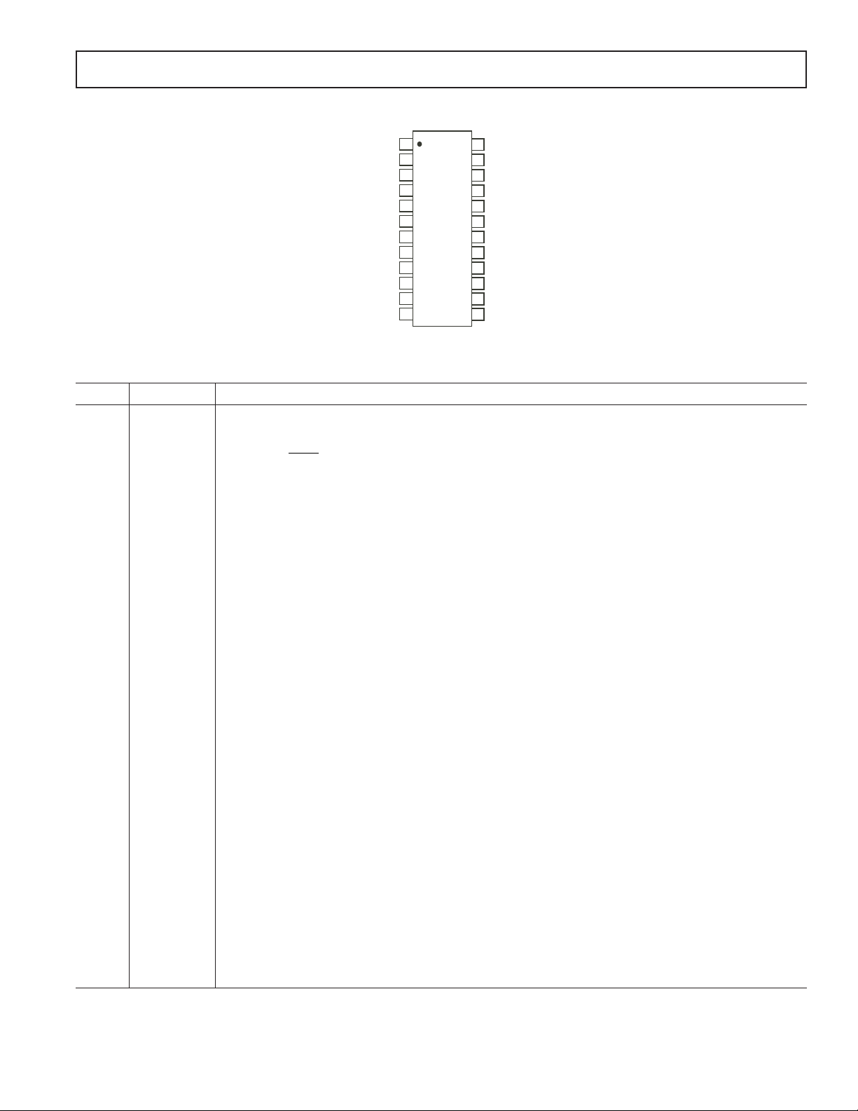
PIN CONFIGURATION
ADF7011
R
SET
CPV
CP
GND
CP
OUT
DATA
CLK
TxDATA
TxCLK
MUXOUT
D
GND
DD
CE
LE
1
2
3
4
5
ADF7011
6
TOP VIEW
(Not to Scale)
7
8
9
10
11
12
TSSOP
24
C
REG
23
C
VCO
22
VCO
IN
21
A
GND
20
RF
OUT
19
RF
GND
18
DV
DD
17
TEST
16
VCO
GND
15
OSC1
14
OSC2
13
CLK
OUT
PIN FUNCTION DESCRIPTIONS
Pin No. Mnemonic Function
1R
2 CPV
SET
DD
External Resistor to Set Change Pump Current and Some Internal Bias Currents. Use 4.7 kΩ as default:
I
CP MAX
So, with R
Charge Pump Supply. This should be biased at the same level as RF
95.
=
R
SET
= 4.7 kΩ, I
SET
CP MAX
= 2.02 mA.
and DVDD. The pin should be
OUT
decoupled with a 0.1 µF capacitor as close to the pin as possible.
3CP
4CP
GND
OUT
Charge Pump Ground.
Charge Pump Output. This output generates current pulses that are integrated in the loop filter. The
integrated current changes the control voltage on the input to the VCO.
5CEChip Enable. A logic low applied to this pin powers down the part. This must be high for the part to
function. This is the only way to power down the regulator circuit.
6 DATA Serial Data Input. The serial data is loaded MSB first with the two LSBs being the control bits. This is a
high impedance CMOS input.
7 CLK Serial Clock Input. This serial clock is used to clock in the serial data to the registers. The data is latched
into the 24-bit shift register on the CLK rising edge. This input is a high impedance CMOS input.
8LELoad Enable, CMOS Input. When LE goes high, the data stored in the shift registers is loaded into one
of the four latches, the latch being selected using the control bits.
9 TxDATA Digital data to be transmitted is input on this pin.
10 TxCLK GFSK Only. This clock output is used to synchronize microcontroller data to the TxDATA pin of the
ADF7011. The clock is provided at the same frequency as the data rate.
11 MUXOUT This multiplexer output allows either the digital lock detect (most common), the scaled RF, or the scaled
reference frequency to be accessed externally. Used commonly for system debug. See the Function Register Map.
12 D
GND
13 CLK
OUT
Ground Pin for the RF Digital Circuitry.
The Divided Down Crystal Reference with 50:50 Mark-Space Ratio. May be used to drive the clock
input of a microcontroller. To reduce spurious components in the output spectrum, the sharp edges can
be reduced with a series RC. For 4.8 MHz output clock, a series 50 Ω into 10 pF will reduce spurs to
< –50 dBc. Defaults on power-up to divide by 16.
14 OSC2 Oscillator Pin. If a single-ended reference (such as a TCXO) is used, it should be applied to this pin.
When using an external signal generator, a 51 Ω resistor should be tied from this pin to ground. The
XOE bit in the R register should set high when using an external reference.
REV. 0
–5–

ADF7011
PIN FUNCTION DESCRIPTIONS (continued)
Pin No. Mnemonic Function
15 OSC1 Oscillator Pin. For use with crystal reference only. This is three-stated when an external reference oscilla-
tor is used.
16 VCO
GND
17 TEST Input to the RF Fractional-N Divider. This pin allows the user to connect an external VCO to the part.
18 DV
19 RF
20 RF
21 A
22 VCO
23 C
24 C
DD
GND
OUT
GND
IN
VCO
REG
Voltage Controlled Oscillator Ground.
Disabling the internal VCO activates this pin. If the internal VCO is used, this pin should be grounded.
Positive Supply for the Digital Circuitry. This must be between 2.3 V and 3.6 V. Decoupling capacitors
to the analog ground plane should be placed as close as possible to this pin.
Ground for Output Stage of Transmitter.
The modulated signal is available at this pin. Output power levels are from –16 dBm to +12 dBm. The
output should be impedance matched to the desired load using suitable components. See the RF Output
Stage section.
Ground Pin for the RF Analog Circuitry.
The tuning voltage on this pin determines the output frequency of the Voltage Controlled Oscillator
(VCO). The higher the tuning voltage, the higher the output frequency.
A 0.22 µF capacitor should be added to reduce noise on VCO bias lines. Tied to the C
A 2.2 µF capacitor should be added at C
, tied to GND, to reduce regulator noise and improve
REG
REG
pin.
stability. A reduced capacitor will improve regulator power-on time but may cause higher spurious
components.
REV. 0–6–
Typical Performance Characteristics–ADF7011
RL = 10.0dBm
VDD = 3V
PFD FREQUENCY = 19.2MHz
LOOP BW = 100kHz
868.3MHz SPAN 5.000MHz
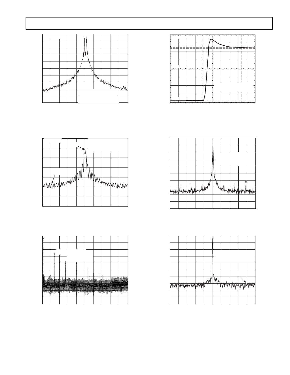
TPC 1. FSK Modulated Signal, F
RBW = 1kHz
DEVIATION
Data Rate = 19.2 kbps, 10 dBm
RL = 10.0dBm
–36dBm
@ 200kHz
–2dBm
VDD = 3V
PFD FREQUENCY = 19.2MHz
LOOP BW = 1MHz
RBW = 3kHz
= 58 kHz,
885.000MHz
868.000MHz
VDD = 3V
PFD FREQUENCY = 19.2MHz
LOOP BW = 100kHz
851.000MHz
5.00s–20.00s
5.00s/DIV
30.00s
TPC 4. PLL Settling Time, 852 MHz to 878 MHz,
23 s (±400 kHz)
+10dBm
VDD = 3V
PFD FREQUENCY = 19.2MHz
LOOP BW = 100kHz
RBW = 100kHz
+19.2MHz
–61dBc
868.3MHz SPAN 500kHz
TPC 2. OOK Modulated Signal, Data Rate = 4.8 kbps,
4 dBm
+10dBm
SECOND HARMONIC
–22dBc
THIRD HARMONIC
–34dBc
START 800MHz STOP 7.750GHz
RBW 1.0MHz
TPC 3. Harmonic Levels at 10 dBm Output Power.
See Figure 15.
RBW 100kHz SPAN 50.00MHz868.3MHz
TPC 5. PFD Spurious/Fractional Spurious Components
+10dBm
VDD = 3V
PFD FREQUENCY = 19.2MHz
LOOP BW = 100kHz
RBW = 30Hz
PN @ 4kHz
80dBc/Hz
SPAN 10.00kHz868.3MHz
TPC 6. In-Band Phase Noise
REV. 0
–7–
ADF7011
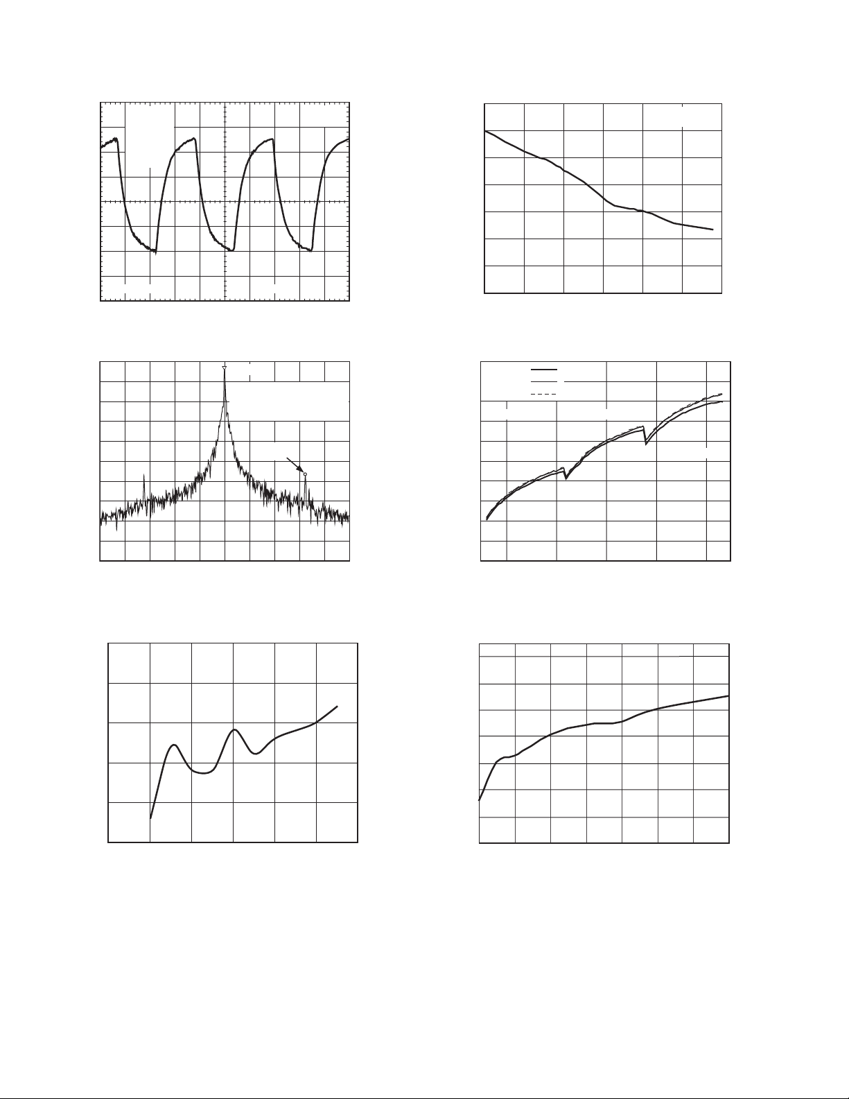
C1 RISE
144.8ns
C1 FALL
145.6ns
C1 +DUTY
49.385%
Ch1 500mV
TPC 7. 1.6 MHz CLOCK
C1 FREQ
1.6MHz
M 200ns
Waveform
OUT
+10dBm
VDD = 3V
PFD FREQUENCY = 19.2MHz
LOOP BW = 100kHz
RBW = 10Hz
+1.6MHz
–53dBc
SPAN 5.00MHz868.3MHz
110
100
90
80
70
GAIN (MHz/V)
60
50
40
885
20
VDD = 2.2V
15
VDD = 3.0V
VDD = 3.6V
10
5
0
–5
–10
LEVEL (dBm)
–15
–20
–25
–30
40
FREQUENCY (MHz)
TPC 10. Typical VCO Gain
MID RANGELOW RANGE
60 80 100 120
PA SETTING (Modulation Register)
VDD = 3V
= 25C
T
A
935
HIGH RANGE
945925915905895
TPC 8. Spurious Signal Generated by CLOCK
0
–5
–10
–15
SENSITIVITY (dBm)
–20
–25
0.8 0.9 1.0 1.1 1.2 1.3 1.4
FREQUENCY (GHz)
TPC 9. N-Divider Input Sensitivity
OUT
TPC 11. PA Output Programmability, TA = 25°C
44
42
40
38
36
CURRENT (mA)
34
32
30
2.2
SUPPLY VOLTAGE (V)
3.43.02.82.62.4
3.2 3.6
TPC 12. IDD vs. VDD @ 10 dBm
REV. 0–8–
 Loading...