

Page 1
4 GHz to 18 GHz Divide-by-4 Prescaler
FEATURES
Divide-by-4 prescaler
High frequency operation: 4 GHz to 18 GHz
Integrated RF decoupling capacitors
Low power consumption
Active mode: 30 mA
Power-down mode: 7 mA
Low phase noise: −150 dBc/Hz
Single dc supply: 3.3 V compatible with ADF4xxx PLLs
Temperature range: −40
Small package: 3 mm × 3 mm LFCSP
APPLICATIONS
PLL frequency range extender
Point-to-point radios
VSAT radios
Communications test equipment
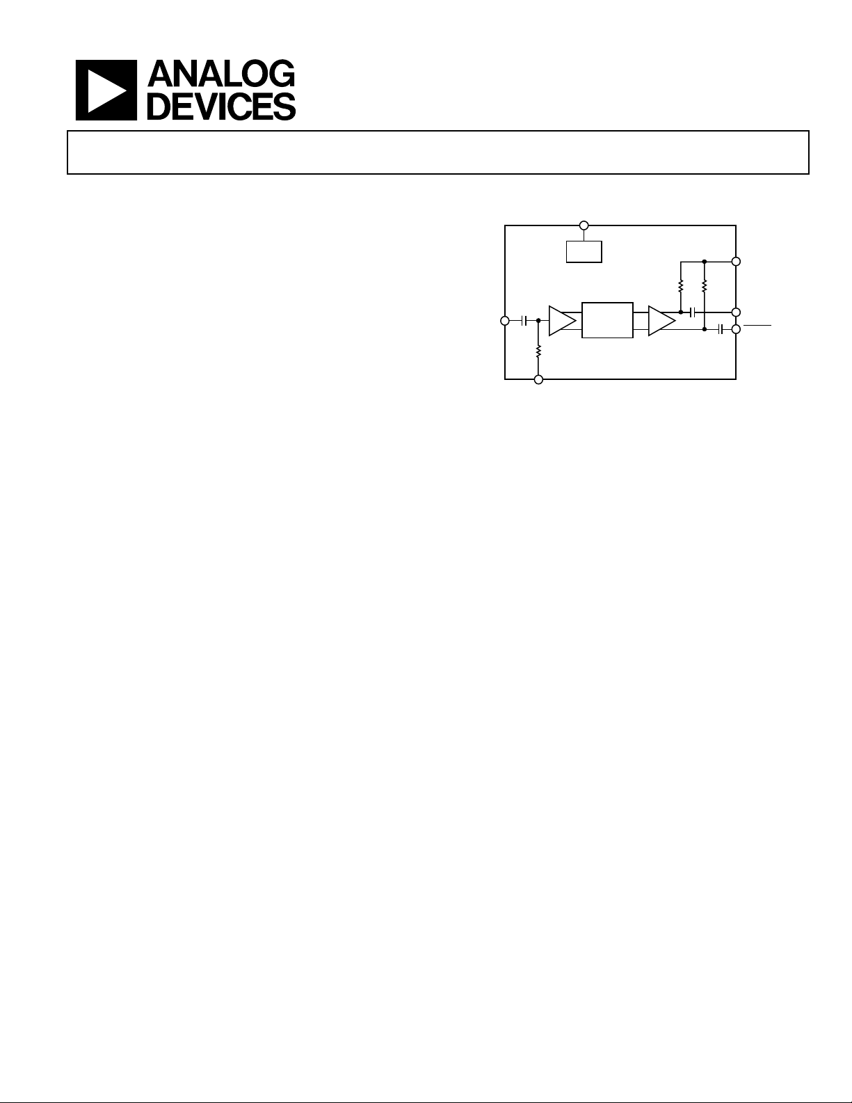
GENERAL DESCRIPTION
The ADF5001 prescaler is a low noise, low power, fixed RF
divider block that can be used to divide down frequencies as
high as 18 GHz to a lower frequency suitable for input into a
PLL IC, such as the ADF4156 or ADF4106. The ADF5001
provides a divide-by-4 function. The ADF5001 operates off a
3.3 V supply and has differential 100 Ω RF outputs to allow
direct interface to the differential RF inputs of PLLs such as the
ADF4156 and ADF4106.
o
C to +105oC
ADF5001
FUNCTIONAL BLOCK DIAGRAM
CE
BIAS
3pF
RFIN
50Ω
GND
DIVIDE
BY 4
Figure 1.
ADF5001
100Ω
1pF
100Ω
1pF
VDDx
RFOUT
RFOUT
08402-001
Rev. A
Information furnished by Analog Devices is believed to be accurate and reliable. However, no
responsibility is assumed by Analog Devices for its use, nor for any infringements of patents or other
rights of third parties that may result from its use. Specifications subject to change without notice. No
license is granted by implication or otherwise under any patent or patent rights of Analog Devices.
Trademarks and registered trademarks are the property of their respective owners.
One Technology Way, P.O. Box 9106, Norwood, MA 02062-9106, U.S.A.
Tel: 781.329.4700 www.analog.com
Fax: 781.461.3113 ©2009–2010 Analog Devices, Inc. All rights reserved.
Page 2

ADF5001
TABLE OF CONTENTS
Features .............................................................................................. 1
Applications ....................................................................................... 1
General Description ......................................................................... 1
Functional Block Diagram .............................................................. 1
Revision History ............................................................................... 2
Specifications ..................................................................................... 3
Absolute Maximum Ratings ............................................................ 4
ESD Caution .................................................................................. 4
REVISION HISTORY
6/10—Rev. 0 to Rev. A
Change to Features Section ............................................................. 1
Change to Applications Section ...................................................... 1
Changes to Figure 1 .......................................................................... 1
Changes to Specifications Section .................................................. 3
Changes to Thermal Impedance Ratings, Table 2 ........................ 4
Changes to Figure 4 Through Figure 7 .......................................... 6
Changes to Evaluation Board PCB Section ................................... 7
Changes to Figure 8 .......................................................................... 7
Change to Table 4 ............................................................................. 7
Changes to Figure 10 ........................................................................ 8
Changes to Ordering Guide ............................................................ 9
10/09—Revision 0: Initial Version
Pin Configuration and Function Descriptions ..............................5
Typical Performance Characteristics ..............................................6
Evaluation Board PCB ......................................................................7
PCB Material Stack-Up ................................................................7
Bill of Materials ..............................................................................7
Application Circuit ............................................................................8
Outline Dimensions ..........................................................................9
Ordering Guide .............................................................................9
Rev. A | Page 2 of 12
Page 3

ADF5001
SPECIFICATIONS
VDD1 = VDD2 = 3.3 V ± 10%, GND = 0 V; dBm referred to 50 Ω; TA = T
range is −40°C to +105°C.
Table 1.
Parameter Min Typ Max Unit Test Conditions/Comments
RF CHARACTERISTICS
Input Frequency 4 18 GHz
RF Input Sensitivity −10 +10 dBm 4 GHz to 18 GHz
Output Power −10 −5 dBm Single-ended output connected into 50 Ω load
−7 −2 dBm
Output Voltage Swing 200 330 mV p-p
400 660 mV p-p
1000 mV p-p
Phase Noise −150 dBc/Hz Input frequency (fIN) = 12 GHz, offset = 100 kHz
Reverse Leakage −60 dBm RF input power (PIN) = 0 dBm, RF
Second Harmonic Content −38 dBc
Third Harmonic Content −12 dBc
Fourth Harmonic Content −20 dBc
Fifth Harmonic Content −19 dBc
CE INPUT
VIH, Input High Voltage 2.2 V
VIL, Input Low Voltage 0.3 V
POWER SUPPLIES
Voltage Supply 3.0 3.3 3.6 V
IDD (IDD1 + IDD2)
Active 30 60 mA CE is high
Power-Down 7 25 mA CE is low
MIN
to T
, unless otherwise noted. The operating temperature
MAX
Differential outputs connected into 100 Ω
differential load
Peak-to-peak voltage swing on each singleended output, connected into 50 Ω load
Peak-to-peak voltage swing on differential
output, connected into 100 Ω differential load
Peak-to-peak voltage swing on each singleended output, no load condition
= 4 GHz
OUT
Rev. A | Page 3 of 12
Page 4
ADF5001
ABSOLUTE MAXIMUM RATINGS
Table 2.
Parameter Rating
VDDx to GND −0.3 V to +3.9 V
RFIN 10 dBm
Operating Temperature Range
Industrial (B Version) −40°C to +105°C
Storage Temperature Range −65°C to +150°C
Maximum Junction Temperature 150°C
LFCSP Thermal Impedance
θ
(Ambient) 90°C/W
JA
θJC(Case) 30°C/W
Peak Temperature 260°C
Time at Peak Temperature 40 sec
Stresses above those listed under Absolute Maximum Ratings
may cause permanent damage to the device. This is a stress
rating only; functional operation of the device at these or any
other conditions above those indicated in the operational
section of this specification is not implied. Exposure to absolute
maximum rating conditions for extended periods may affect
device reliability.
This device is a high performance RF integrated circuit with an
ESD rating of 2 kV, human body model (HBM) and is ESD
sensitive. Proper precautions should be taken for handling and
assembly.
ESD CAUTION
Rev. A | Page 4 of 12
Page 5

ADF5001
PIN CONFIGURATION AND FUNCTION DESCRIPTIONS
1
VDD
GND
GND
VDD2
14
13
15
16
PIN 1
INDICATOR
1GND
2RFIN
ADF5001
3GND
TOP VIEW
(Not to S cale)
4GND
5
6
NC
GND
NOTES
1. NC = NO CONNECT.
2. THE EXPOSED PADDLE MUST BE
CONNECTED TO GND.
Figure 2. Pin Configuration
Table 3. Pin Function Descriptions
Pin No. Mnemonic Description
1, 3, 4, 5, 8, 9, 12,
GND RF Ground. All ground pins should be tied together.
13, 16
2 RFIN Single-Ended 50 Ω Input to the RF Prescaler. This pin is ac-coupled internally via a 3 pF capacitor.
6 NC No Connect. This pin can be left unconnected.
7 CE
Chip Enable. This pin is active high. When CE is brought low, the part enters into power-down mode. If
this functionality is not required, the pin can remain unconnected because it is pulled up internally
through a weak pull-up resistor.
10 RFOUT
Divided Down Output of the Prescaler. This pin has an internal 100 Ω load resistor tied to VDD2 and an
ac-coupling capacitor of 1 pF.
11
Complementary Divided Down Output of the Prescaler. This pin has an internal 100 Ω load resistor tied
RFOUT
to VDD2 and an ac-coupling capacitor of 1 pF.
14 VDD2
Voltage Supply for the Output Stage. Decouple this pin to ground with a 1 nF capacitor and tie it
directly to VDD1.
15 VDD1 Voltage Supply for the Input Stage and Divider Block. Decouple this pin to ground with a 1 nF capacitor.
N/A1 EP The LFCSP package has an exposed paddle that must be connected to GND.
1
N/A means not applicable.
12 GND
11 RFOUT
10 RFOUT
9GND
8
7
CE
GND
08402-002
Rev. A | Page 5 of 12
Page 6

ADF5001
–
TYPICAL PERFORMANCE CHARACTERISTICS
0
–10
5
FIRST HARMO NIC
–10
–20
–30
–40
MINIMUM INPUT POWER (dBm)
–50
ROOM TEMPERAT URE
VDD1 = VDD2 = 3.3V
–60
0 5 10 15 20 25
FREQUENCY (GHz)
Figure 3. RFIN Sensitivity
20
18
16
14
12
10
IDDx (mA)
8
6
4
2
0
2.5 3.93.73.53.33.12.92.7
IDD1
IDD2
VDDx (V)
–15
–20
–25
POWER (dBm)
–30
–35
–40
2.4 2.7 3.0 3.3 3.6
8402-003
VDDx (V)
THIRD HARMONIC
FIFTH HARM ONIC
FOURTH HARMONI C
08402-006
Figure 6. RFOUT Harmonic Content
0
–5
–10
–15
–20
OUTPUT PO WER (dBm)
–25
–30
0
08402-004
INPUT FREQUENCY (GHz)
30252015105
08402-007
Figure 4. IDD1 and IDD2 vs. VDDx
0
–2
–4
–6
–8
–10
–12
–14
RF OUTPUT P OWER (dBm)
–16
–18
–20
2.5 3.93.73.53.33.12.92.7
VDDx (V)
Figure 5. RFOUT Power (Single-Ended) vs. VDDx, fIN = 10 GHz, PIN = 0 dBm
08402-005
Rev. A | Page 6 of 12
Figure 7. RFOUT Power vs. RFIN Frequency, f
= 10 GHz, VDD = 3.3 V
IN
Page 7

ADF5001
EVALUATION BOARD PCB
The evaluation board has four connectors as shown in Figure 8.
The RF input connector (J4) is a high frequency precision SMA
connector from Emerson. This connector is mechanically
compatible with SMA/3.5 mm and 2.92 mm cables.
Figure 8. Evaluation Board Silkscreen—Top View
The evaluation board is powered from a single 3.0 V to 3.6 V
supply, which should be connected to the J1 SMA connector.
The power supply can also be connected using the T3 (VDDx)
and T2 (GND) test points.
The differential RF outputs are brought out on the J2 and J3
SMA connectors. If only one of the outputs is being used, the
unused output should be correctly terminated using a 50 Ω
SMA termination.
The chip enable (CE) pin can be controlled using the T1 test
point. If this function is not required, the test point can remain
unconnected.
PCB MATERIAL STACK-UP
The evaluation board is built using Rogers RO4003C material
(0.008 in.). RF track widths are 0.015 in. to achieve a controlled
50 Ω characteristic impedance. The complete PCB stack-up is
shown in Figure 9.
08753-008
1.5oz (53µm) FINISHED COPPER
ROGERS RO 4003C LAMINATE 0.008”
Er = 3.38. STARTING COPPER WEIGHT 0.5oz/0.5o z
0.5oz (18µm) FINISHED COPPER
FR4 PREPREG
0.0372”
0.5oz (18µm) FINISHED COPPER
ROGERS RO 4003C LAMINATE 0.008”
Er = 3.38.STARTING COPPER WEIGHT 0.5oz/0.5o z
1.5oz (53µm) FINISHED COPPER
Figure 9. Evaluation Board PCB Layer Stack-Up
BILL OF MATERIALS
Table 4.
Reference
Qty.
Designator
1 C1 0.1 μF, 0603
1 C2 10 pF, 0402
1 J4 3.5 mm RF SMA
3 J1, J2, J3 3.5 mm RF SMA
3 T1, T2, T3 Test points
1 U1 ADF5001 RF
Description Supplier/Part Number
capacitor
capacitor
connector
connector
prescaler
0.062” ± 0.003”
COPPER TO COPPER
08402-009
Murata
GRM188R71H104KA93D
Murata
GRM1555C1H100JZ01D
Emerson 142-0761-801
Johnson Components
142-0701-851
Vero 20-2137
Analog Devices, Inc.,
ADF5001BCPZ
Rev. A | Page 7 of 12
Page 8

ADF5001
APPLICATION CIRCUIT
The ADF5001 can be connected either single-ended or differentially to any of the Analog Devices PLL family of ICs. It is recommended to use a differential connection for best performance
and to achieve maximum power transfer. The application circuit
shown in Figure 10 shows the ADF5001 used as the RF prescaler
in a microwave 16 GHz PLL loop. The ADF5001 divides down
the 16 GHz RF signal to 4 GHz, which is input differentially
into the ADF4156 PLL. An active filter topology, using the
OP184 op amp, is used to provide the wide tuning ranges
10pF 0.1µF
VDD1
RFIN
VDD2
ADF5001
PRESCALER
GND
RFOUT
RFOUT
DECOUPLING
INTEGRATED
RF
RF
ADF4156
A
IN
B
IN
PLL
typically required by microwave VCOs. The positive input pin of
the OP184 is biased at half the ADF4156 charge pump supply
(VP). This can be easily achieved using a simple resistor divider,
ensuring sufficient decoupling close to the +IN A pin of the
OP184 thereby allowing the use of a single positive supply for the
op amp. Alternatively, to optimize performance by ensuring a
clean bias voltage, a low noise regulator like the ADP150 can be
used to power the resistor divider network or the +IN A pin
directly.
1.8nF
47nF
330Ω
CP
220Ω
820pF
VP/2
1µF
OP184
OP AMP
1kΩ
1.8nF
6dB PAD
37Ω
150Ω150Ω
18Ω
18Ω
16GHz OUT
MICROWAVE
VCO
RFOUT VTUNE
08402-010
Figure 10. ADF5001 Used as the RF Prescaler in a Microwave 16 GHz PLL Loop
Rev. A | Page 8 of 12
Page 9

ADF5001
OUTLINE DIMENSIONS
PIN 1
INDICATOR
0.80
0.75
0.70
SEATING
PLANE
3.10
3.00 SQ
2.90
0.50
BSC
0.45
0.40
0.35
0.05 MAX
0.02 NOM
0.20 REF
0.30
0.25
0.18
13
12
9
8
BOTTOM VIEWTOP VIEW
COPLANARITY
0.08
1
P
N
I
C
I
A
N
I
16
EXPOSED
PAD
5
FOR PROPER CONNECTION O F
THE EXPOSED PAD, REFER TO
THE PIN CONF IGURATIO N AND
FUNCTION DESCRI P T I O NS
SECTION O F THIS DATA SHEET.
D
1
1.60
1.50 SQ
1.40
4
0.25 MIN
R
O
T
COMPLIANTTOJEDEC STANDARDS MO-220- W E ED-6.
111808-A
Figure 11. 16-Lead Lead Frame Chip Scale Package [LFCSP_WQ]
3 mm × 3 mm Body, Very Very Thin Quad
(CP-16-18)
Dimensions shown in millimeters
ORDERING GUIDE
Temperature
Model1
Range Package Description
ADF5001BCPZ −40°C to +105°C 16-Lead Lead Frame Chip Scale Package (LFCSP_WQ) CP-16-18 Q1S
ADF5001BCPZ-RL7 −40°C to +105°C
16-Lead Lead Frame Chip Scale Package (LFCSP_WQ), 7” Tape
and Reel
EVAL-ADF5001EB2Z Evaluation Board
1
Z = RoHS Compliant Part.
Package
Option Branding
CP-16-18
Q1S
Rev. A | Page 9 of 12
Page 10

ADF5001
NOTES
Rev. A | Page 10 of 12
Page 11

ADF5001
NOTES
Rev. A | Page 11 of 12
Page 12

ADF5001
NOTES
©2009–2010 Analog Devices, Inc. All rights reserved. Trademarks and
registered trademarks are the property of their respective owners.
D08402-0-6/10(A)
Rev. A | Page 12 of 12
 Loading...