Analog Devices ADF4360 7 a Datasheet
FEATURES
Output frequency range: 350 MHz to 1800 MHz
Divide-by-2 output
3.0 V to 3.6 V power supply
1.8 V logic compatibility
Integer-N synthesizer
Programmable dual-modulus prescaler 8/9, 16/17
Programmable output power level
3-wire serial interface
Analog and digital lock detect
Hardware and software power-down mode
APPLICATIONS
Wireless handsets (DECT, GSM, PCS, DCS, WCDMA)
Test equipment
Wireless LANs
CATV equipment
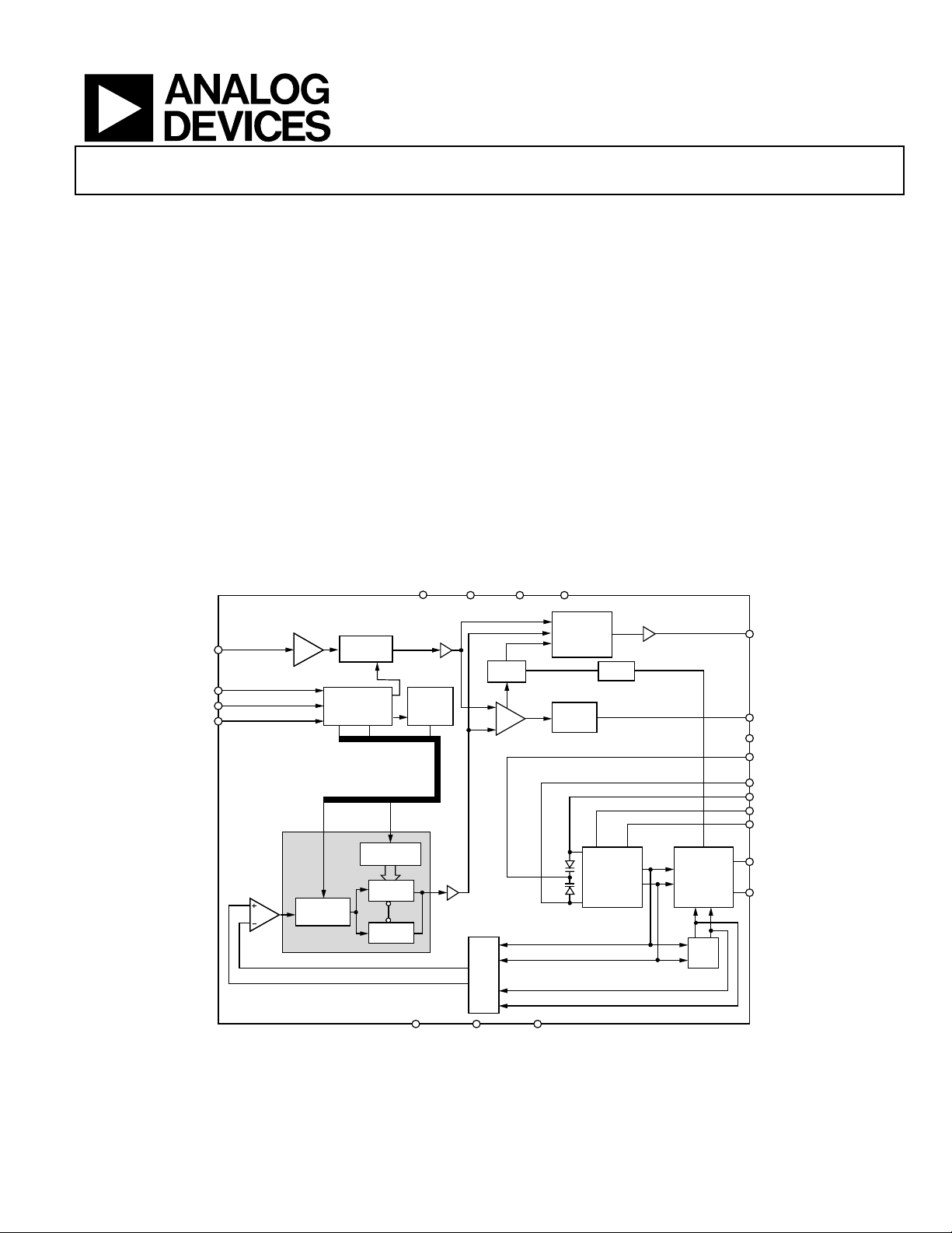
FUNCTIONAL BLOCK DIAGRAM
Integrated Synthesizer and VCO
ADF4360-7
GENERAL DESCRIPTION
The ADF4360-7 is an integrated integer-N synthesizer and
voltage controlled oscillator (VCO). The ADF4360-7 center
frequency is set by external inductors. This allows a frequency
range of between 350 MHz to 1800 MHz. In addition, a divideby-2 option is available, whereby the user receives an RF output
of between 175 MHz and 900 MHz.
Control of all the on-chip registers is through a simple 3-wire
interface. The device operates with a power supply ranging from
3.0 V to 3.6 V and can be powered down when not in use.
AV
DV
DD
R
DD
CE
SET
REF
CLK
DATA
ADF4360-7
MUXOUT
CP
V
VCO
V
TUNE
L1
L2
C
C
C
N
RF
OUT
RF
OUT
04441-001
A
B
DIVSEL = 1
DIVSEL = 2
MULTIPLEXER
CHARGE
PUMP
MUTE
VCO
CORE
OUTPUT
STAGE
÷2
DATA REGISTER
P/P+1
14-BIT R
COUNTER
24-BIT
LOAD
LOAD
24-BIT
FUNCTION
LATCH
INTEGER
REGISTER
13-BIT B
COUNTER
5-BIT A
COUNTER
AGND DGND CPGND
LOCK
DETECT
PHASE
COMPARATOR
MULTIPLEXER
IN
LE
PRESCALER
N = (BP + A)
Figure 1.
Rev. A
Information furnished by Analog Devices is believed to be accurate and reliable.
However, no responsibility is assumed by Analog Devices for its use, nor for any
infringements of patents or other rights of third parties that may result from its use.
Specifications subject to change without notice. No license is granted by implication
or otherwise under any patent or patent rights of Analog Devices. Trademarks and
registered trademarks are the property of their respective owners.
One Technology Way, P.O. Box 9106, Norwood, MA 02062-9106, U.S.A.
Tel: 781.329.4700
Fax: 781.326.8703 © 2004 Analog Devices, Inc. All rights reserved.
www.analog.com

ADF4360-7
TABLE OF CONTENTS
Specifications..................................................................................... 3
Output Stage................................................................................ 12
Timing Characteristics..................................................................... 5
Absolute Maximum Ratings............................................................ 6
Transis t o r Cou nt ........................................................................... 6
ESD Caution.................................................................................. 6
Pin Configuration and Function Descriptions............................. 7
Typical Performance Characteristics............................................. 8
Circuit Description......................................................................... 10
Reference Input Section............................................................. 10
Prescaler (P/P + 1)...................................................................... 10
A and B Counters ....................................................................... 10
R Counter ....................................................................................10
PFD and Charge Pump.............................................................. 10
MUXOUT and Lock Detect...................................................... 11
Input Shift Register..................................................................... 11
VCO.............................................................................................. 11
Latch Structure ........................................................................... 13
Power-Up..................................................................................... 17
Control Latch.............................................................................. 19
N Counter Latch......................................................................... 20
R Counter Latch ......................................................................... 20
Applications..................................................................................... 21
Frequency Generator ................................................................. 21
Choosing the Correct Inductance Value................................. 22
Fixed Frequency LO ................................................................... 22
Interfacing ................................................................................... 23
PCB Design Guidelines for Chip Scale Package........................... 23
Output Matching........................................................................ 24
Outline Dimensions....................................................................... 25
Ordering Guide .......................................................................... 25
REVISION HISTORY
11/04—Rev. 0 to Rev. A.
Updated Format..................................................................Universal
Changes to General Description .................................................... 1
Changes to Specifications................................................................ 3
Changes to the Reference Input Section...................................... 10
Changes to Power-Up Section ...................................................... 17
Added Table 10 ............................................................................... 17
Added Figure 22.............................................................................. 17
Updated Outline Dimensions....................................................... 25
2/04—Revision 0: Initial Version.
Rev. A | Page 2 of 28

ADF4360-7
SPECIFICATIONS
AVDD = DVDD = V
Table 1.
Parameter B Version Unit Conditions/Comments
REFIN CHARACTERISTICS
REFIN Input Frequency 10/250 MHz min/max
REFIN Input Sensitivity 0.7/AV
0 to AVDD V max CMOS compatible.
REFIN Input Capacitance 5.0 pF max
REFIN Input Current ±60 µA max
PHASE DETECTOR
Phase Detector Frequency2 8 MHz max
CHARGE PUMP
ICP Sink/Source3 With R
High Value 2.5 mA typ
Low Value 0.312 mA typ
R
Range 2.7/10 kΩ
SET
ICP Three-State Leakage Current 0.2 nA typ
Sink and Source Current Matching 2 % typ 1.25 V ≤ VCP ≤ 2.5 V.
ICP vs. VCP 1.5 % typ 1.25 V ≤ VCP ≤ 2.5 V.
ICP vs. Temperature 2 % typ VCP = 2.0 V.
LOGIC INPUTS
V
, Input High Voltage 1.5 V min
INH
V
, Input Low Voltage 0.6 V max
INL
I
, Input Current ±1 µA max
INH/IINL
CIN, Input Capacitance 3.0 pF max
LOGIC OUTPUTS
VOH, Output High Voltage DVDD – 0.4 V min CMOS output chosen.
IOH, Output High Current 500 µA max
VOL, Output Low Voltage 0.4 V max IOL = 500 µA.
POWER SUPPLIES
AVDD 3.0/3.6 V min/V max
DVDD AV
V
AV
VCO
4
AI
DD
4
DI
DD
, 5
4
I
VCO
4
I
RFOUT
Low Power Sleep Mode 7 µA typ
Specifications continued on next page.
VCO
1
= 3.3 V ± 10%; AGND = DGND = 0 V; TA = T
DD
DD
DD
V p-p min/max AC-coupled.
10 mA typ
2.5 mA typ
14.0 mA typ I
3.5 to 11.0 mA typ RF output stage is programmable.
MIN
to T
, unless otherwise noted.
MAX
For f < 10 MHz, use a dc-coupled CMOS-compatible
square wave, slew rate > 21 V/µs.
= 4.7 kΩ.
SET
= 5 mA.
CORE
Rev. A | Page 3 of 28

ADF4360-7
Parameter B Version Unit Conditions/Comments
RF OUTPUT CHARACTERISTICS5
Maximum VCO Output Frequency 1800 MHz
Minimum VCO Output Frequency 350 MHz
VCO Output Frequency 490/585 MHz min/max
VCO Frequency Range 1.2 Ratio F
VCO Sensitivity 12 MHz/V typ
Lock Time
6
400 µs typ To within 10 Hz of final frequency.
Frequency Pushing (Open Loop) 6 MHz/V typ
Frequency Pulling (Open Loop) 15 kHz typ Into 2.00 VSWR load.
Harmonic Content (Second) −19 dBc typ
Harmonic Content (Third) −9 dBc typ
Output Power
5, 7
−14/−5 dBm typ Programmable in 3 dB steps. See Table 7.
Output Power Variation ±3 dB typ For tuned loads, see Output Matching section.
VCO Tuning Range 1.25/2.5 V min/max
NOISE CHARACTERISTIC
5
VCO Phase-Noise Performance8 −116 dBc/Hz typ @ 100 kHz offset from carrier.
−138 dBc/Hz typ @ 1 MHz offset from carrier.
−144 dBc/Hz typ @ 3 MHz offset from carrier.
−148 dBc/Hz typ @ 10 MHz offset from carrier.
Synthesizer Phase-Noise Floor
9
−172 dBc/Hz typ @ 25 kHz PFD frequency.
−163 dBc/Hz typ @ 200 kHz PFD frequency.
−147 dBc/Hz typ @ 8 MHz PFD frequency.
In-Band Phase Noise
10, 11
−92 dBc/Hz typ @ 1 kHz offset from carrier.
RMS Integrated Phase Error12 0.3 Degrees typ 100 Hz to 100 kHz.
Spurious Signals due to PFD
Frequency
11, 13
−70 dBc typ
Level of Unlocked Signal with
−44 dBm typ
MTLD Enabled
1
Operating temperature range is –40°C to +85°C.
2
Guaranteed by design. Sample tested to ensure compliance.
3
ICP is internally modified to maintain constant loop gain over the frequency range.
4
TA = 25°C; AVDD = DVDD = V
5
Unless otherwise stated, these characteristics are guaranteed for VCO core power = 5 mA. L1, L2 = 13 nH, 470 Ω resistors to GND in parallel with L1, L2.
6
Jumping from 490 MHz to 585 MHz. PFD frequency = 200 kHz; loop bandwidth = 10 kHz.
7
Using 50 Ω resistors to V
8
The noise of the VCO is measured in open-loop conditions.
9
The synthesizer phase-noise floor is estimated by measuring the in-band phase noise at the output of the VCO and subtracting 20 log N (where N is the N divider value).
10
The phase noise is measured with the EVAL-ADF4360-xEB1 Evaluation Board and the HP 8562E Spectrum Analyzer. The Spectrum Analyzer provides the REFIN for the
synthesizer; offset frequency = 1 kHz.
11
f
= 10 MHz; f
REFIN
12
f
= 10 MHz; f
REFIN
13
The spurious signals are measured with the EVAL-ADF4360-xEB1 Evaluation Board and the HP 8562E Spectrum Analyzer. The Spectrum Analyzer provides the REFIN
for the synthesizer; f
= 200 kHz; N = 2500; loop B/W = 10 kHz.
PFD
= 1 MHz; N = 500; loop B/W = 25 kHz.
PFD
= 3.3 V; P = 32.
VCO
, into a 50 Ω load. For tuned loads, see the Output M section. atching
VCO
= 10 MHz @ 0 dBm.
REFOUT
= 5 mA. Depending on L. See the Choosing the Correct
I
CORE
Inductance Value section.
L1, L2 = 13 nH. See the Choosing the Correct Inductance Value
section for other frequency values.
MAX/FMIN
L1, L2 = 13 nH. See the Choosing the Correct Inductance Value
section for other sensitivity values.
Rev. A | Page 4 of 28
ADF4360-7
K
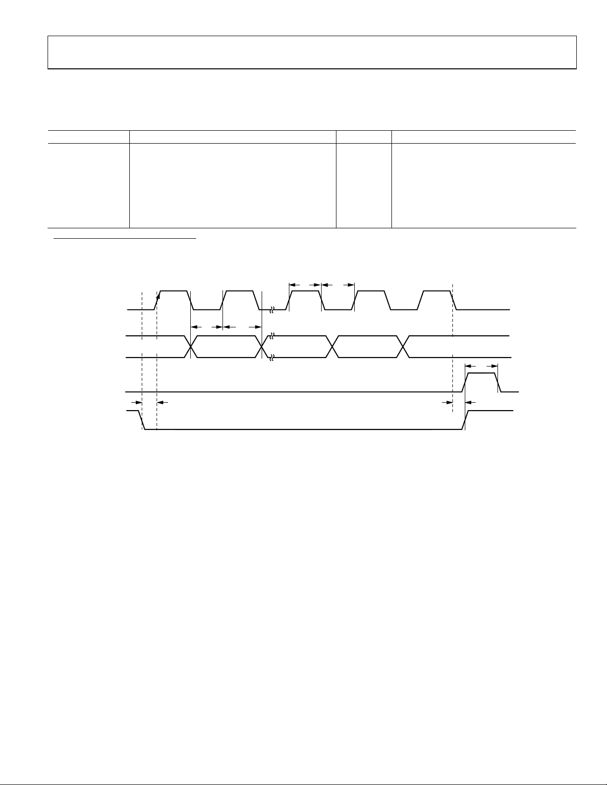
TIMING CHARACTERISTICS
AVDD = DVDD = V
Table 2.
Parameter Limit at T
t1 20 ns min LE Setup Time
t2 10 ns min DATA to CLOCK Setup Time
t3 10 ns min DATA to CLOCK Hold Time
t4 25 ns min CLOCK High Duration
t5 25 ns min CLOCK Low Duration
t6 10 ns min CLOCK to LE Setup Time
t7 20 ns min LE Pulse Width
1
Refer to the section for the recommended power-up procedure for this device. Power-Up
= 3.3 V ± 10%; AGND = DGND = 0 V; 1.8 V and 3 V logic levels used; TA = T
VCO
MIN
1
to T
MIN
to T
(B Version) Unit Test Conditions/Comments
MAX
, unless other wise noted.
MAX
CLOC
DATA
t
2
DB23 (MSB) DB22 DB2
LE
t
1
LE
t
t
4
3
t
5
DB1
(CONTROL BIT C2)
DB0 (LSB)
(CONTROL BIT C1)
t
6
t
7
04441-002
Figure 2. Timing Diagram
Rev. A | Page 5 of 28
ADF4360-7
ABSOLUTE MAXIMUM RATINGS
TA = 25°C, unless otherwise noted.
Table 3.
Parameter Rating
AVDD to GND
AVDD to DVDD −0.3 V to +0.3 V
V
to GND −0.3 V to +3.9 V
VCO
V
to AVDD −0.3 V to +0.3 V
VCO
Digital I/O Voltage to GND −0.3 V to VDD + 0.3 V
Analog I/O Voltage to GND −0.3 V to VDD + 0.3 V
REFIN to GND −0.3 V to VDD + 0.3 V
Operating Temperature Range
Maximum Junction Temperature 150°C
CSP θJA Thermal Impedance
Paddle Soldered 50°C/W
Paddle Not Soldered 88°C/W
Lead Temperature, Soldering
Vapor Phase (60 sec) 215°C
Infrared (15 sec) 220°C
1
−0.3 V to +3.9 V
1
GND = AGND = DGND = 0 V.
Stresses above those listed under Absolute Maximum Ratings
may cause permanent damage to the device. This is a stress rating only; functional operation of the device at these or any
other conditions above those listed in the operational sections
of this specification is not implied. Exposure to absolute maximum rating conditions for extended periods may affect device
reliability.
This device is a high performance RF integrated circuit with an
ESD rating of <1 kV, and it is ESD sensitive. Proper precautions
should be taken for handling and assembly.
TRANSISTOR COUNT
12543 (CMOS) and 700 (Bipolar)
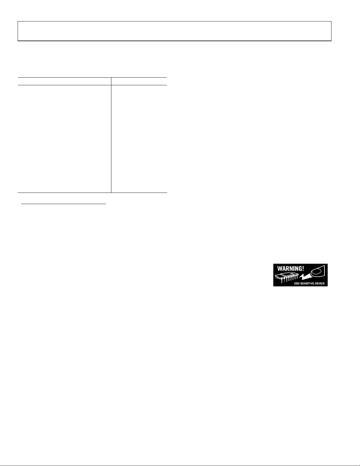
ESD CAUTION
ESD (electrostatic discharge) sensitive device. Electrostatic charges as high as 4000 V readily accumulate
on the human body and test equipment and can discharge without detection. Although this product features
proprietary ESD protection circuitry, permanent damage may occur on devices subjected to high energy
electrostatic discharges. Therefore, proper ESD precautions are recommended to avoid performance
degradation or loss of functionality.
Rev. A | Page 6 of 28
ADF4360-7
T
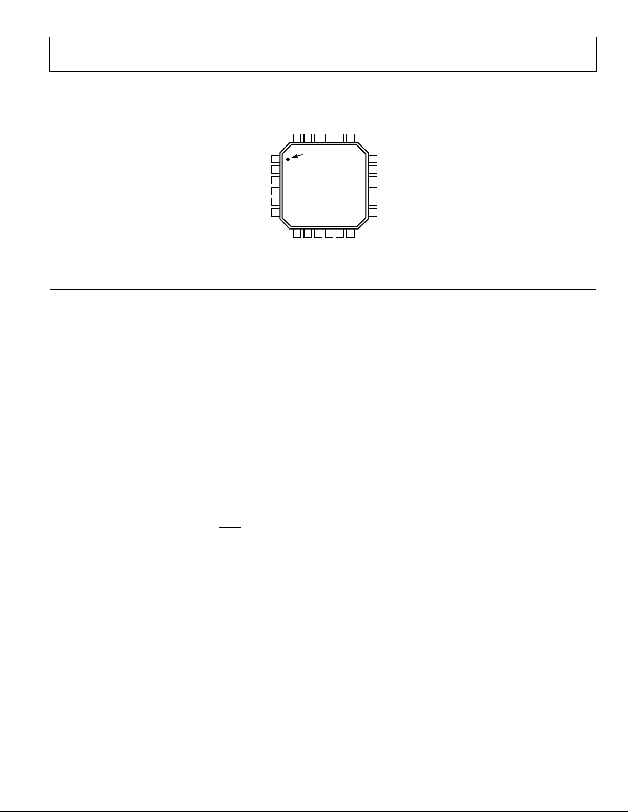
PIN CONFIGURATION AND FUNCTION DESCRIPTIONS
DD
21
PIN 1
IDENTIFIER
ADF4360-7
TOP VIEW
(Not to Scale)
8L19
10
L2
AGND
MUXOU
20LE19
11
AGND
18
DATA
CLK
17
REF
16
IN
DGND
15
C
14
N
R
13
SET
12
C
C
04441-003
CPGND
AV
AGND
RF
OUT
RF
OUT
V
VCO
CP24CE23AGND22DV
1
2
DD
3
A
4
B
5
6
7
TUNE
V
Figure 3. Pin Configuration
Table 4. Pin Function Descriptions
Pin No. Mnemonic Function
1 CPGND Charge Pump Ground. This is the ground return path for the charge pump.
2 AVDD Analog Power Supply. This ranges from 3.0 V to 3.6 V. Decoupling capacitors to the analog ground plane should be
placed as close as possible to this pin. AV
must have the same value as DVDD.
DD
3, 8, 11, 22 AGND Analog Ground. This is the ground return path of the prescaler and VCO.
4 RF
A VCO Output. The output level is programmable from −5 dBm to −14 dBm. See the Output Matching section for a
OUT
description of the various output stages.
5 RF
B VCO Complementary Output. The output level is programmable from −5 dBm to −14 dBm. See the Output Matching
OUT
section for a description of the various output stages.
6 V
7 V
Power Supply for the VCO. This ranges from 3.0 V to 3.6 V. Decoupling capacitors to the analog ground plane should
VCO
be placed as close as possible to this pin. V
Control Input to the VCO. This voltage determines the output frequency and is derived from filtering the CP output
TUNE
must have the same value as AVDD.
VCO
voltage.
9 L1 An external inductor to AGND should be connected to this pin to set the ADF4360-7 output frequency. L1 and L2
need to be the same value. For inductances greater than 3.3 nH, a 470 Ω resistor should be added in parallel to AGND.
10 L2 An external inductor to AGND should be connected to this pin to set the ADF4360-7 output frequency. L1 and L2
need to be the same value. For inductances greater than 3.3 nH, a 470 Ω resistor should be added in parallel to AGND.
12 C
13 R
14 C
C
Connecting a resistor between this pin and CPGND sets the maximum charge pump output current for the
SET
N
Internal Compensation Node. This pin must be decoupled to ground with a 10 nF capacitor.
synthesizer. The nominal voltage potential at the R
I
where R
11.75
=
CPmax
R
= 4.7 kΩ, and I
SET
SET
= 2.5 mA.
CPmax
Internal Compensation Node. This pin must be decoupled to V
pin is 0.6 V. The relationship between ICP and R
SET
with a 10 µF capacitor.
VCO
is
SET
15 DGND Digital Ground.
16 REFIN Reference Input. This is a CMOS input with a nominal threshold of VDD/2 and a dc equivalent input resistance of
100 kΩ (see Figure 16). This input can be driven from a TTL or CMOS crystal oscillator, or it can be ac-coupled.
17 CLK Serial Clock Input. This serial clock is used to clock in the serial data to the registers. The data is latched into the 24-bit
shift register on the CLK rising edge. This input is a high impedance CMOS input.
18 DATA Serial Data Input. The serial data is loaded MSB first with the two LSBs being the control bits. This input is a high
impedance CMOS input.
19 LE Load Enable, CMOS Input. When LE goes high, the data stored in the shift registers is loaded into one of the four
latches, and the relevant latch is selected using the control bits.
20 MUXOUT This multiplexer output allows either the lock detect, the scaled RF, or the scaled reference frequency to be accessed
externally.
21 DVDD Digital Power Supply. This ranges from 3.0 V to 3.6 V. Decoupling capacitors to the digital ground plane should be
placed as close as possible to this pin. DV
must have the same value as AVDD.
DD
23 CE Chip Enable. A logic low on this pin powers down the device and puts the charge pump into three-state mode.
Taking the pin high powers up the device depending on the status of the power-down bits.
24 CP Charge Pump Output. When enabled, this provides ± ICP to the external loop filter, which in turn drives the internal VCO.
Rev. A | Page 7 of 28
ADF4360-7
TYPICAL PERFORMANCE CHARACTERISTICS
–40
–50
–60
–70
–80
–90
–100
–110
OUTPUT POWER (dB)
–120
–130
–140
–150
100 1k 10k 100k 1M 10M
FREQUENCY OFFSET (Hz)
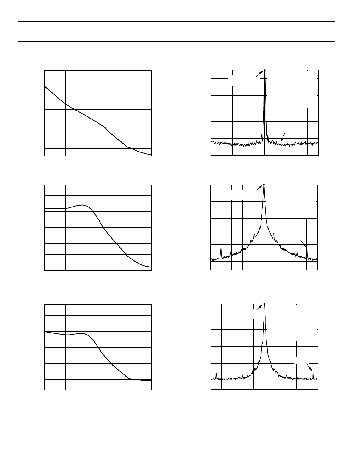
Figure 4. Open-Loop VCO Phase Noise, L1, L2 = 13 nH
04441-004
–10
–20
–30
–40
–50
–60
–70
OUTPUT POWER (dB)
–80
–90
0
REFERENCE
LEVEL = –3.5dBm
–2kHz –1kHz 500MHz 1kHz 2kHz
VDD = 3.3V, V
I
= 2.5mA
CP
PFD FREQUENCY = 200kHz
LOOP BANDWIDTH = 10kHz
RES. BANDWIDTH = 30Hz
VIDEO BANDWIDTH = 30Hz
SWEEP = 1.9 SECONDS
AVERAGES = 10
VCO
–96.4dBc/Hz
= 3.3V
Figure 7. Close-In Phase Noise at 500 MHz (200 kHz Channel Spacing)
04441-007
–70
–75
–80
–85
–90
–95
–100
–105
–110
–115
–120
–125
OUTPUT POWER (dB)
–130
–135
–140
–145
–150
100 1k 10k 100k 1M 10M
FREQUENCY OFFSET (Hz)
04441-005
Figure 5. VCO Phase Noise, 500 MHz, 200 kHz PFD, 10 kHz Loop Bandwidth
–70
–75
–80
–85
–90
–95
–100
–105
–110
–115
–120
–125
OUTPUT POWER (dB)
–130
–135
–140
–145
–150
100 1k 10k 100k 1M 10M
FREQUENCY OFFSET (Hz)
04441-006
Figure 6. VCO Phase Noise, 250 MHz,
Divide-by-2 Enabled 200 kHz PFD, 10 kHz Loop Bandwidth
0
–10
–20
–30
–40
–50
–60
–70
OUTPUT POWER (dB)
–80
–90
–0.25MHz –0.1MHz 1250MHz 0.1MHz 0.25MHz
REFERENCE
LEVEL = –3dBm
VDD = 3.3V, V
I
= 2.5mA
CP
PFD FREQUENCY = 200kHz
LOOP BANDWIDTH = 10kHz
RES. BANDWIDTH = 1kHz
VIDEO BANDWIDTH = 1kHz
AVERAGES = 20
= 3.3V
VCO
–74dBc
Figure 8. Reference Spurs at 500 MHz
(200 kHz Channel Spacing, 10 kHz Loop Bandwidth)
0
–10
–20
–30
–40
–50
–60
–70
OUTPUT POWER (dB)
–80
–90
–1.1MHz –0.55MHz 500MHz 0.55MHz 1.1MHz
REFERENCE
LEVEL = –3dBm
VDD = 3.3V, V
I
= 2.5mA
CP
PFD FREQUENCY = 1MHz
LOOP BANDWIDTH = 25kHz
RES. BANDWIDTH = 1kHz
VIDEO BANDWIDTH = 1kHz
SWEEP = 4.2 SECONDS
AVERAGES = 20
VCO
= 3.3V
–79dBc
Figure 9. Reference Spurs at 500 MHz
(1 MHz Channel Spacing, 25 kHz Loop Bandwidth)
04441-008
04441-009
Rev. A | Page 8 of 28
ADF4360-7
z
–40
–50
–60
–70
–80
–90
–100
–110
OUTPUT POWER (dB)
–120
–130
–140
–150
100 1k 10k 100k 1M 10M
FREQUENCY OFFSET (Hz)
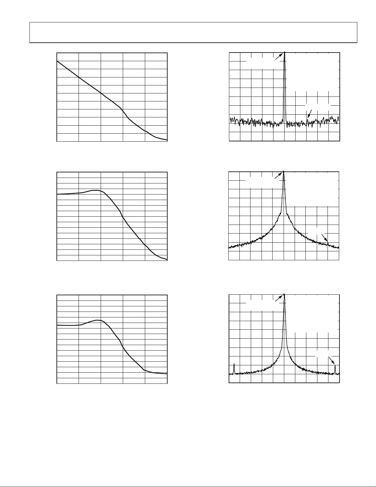
Figure 10. Open-Loop VCO Phase Noise, L1 and L2 = 1.0 nH
04441-010
0
–10
–20
–30
–40
–50
–60
–70
OUTPUT POWER (dB)
–80
–90
REFERENCE
LEVEL = –3.5dBm
–2kHz –1kHz 1.25GHz 1kHz 2kHz
VDD = 3.3V, V
I
= 2.5mA
CP
PFD FREQUENCY = 200kHz
LOOP BANDWIDTH = 10kHz
RES. BANDWIDTH = 30Hz
VIDEO BANDWIDTH = 30Hz
SWEEP = 1.9 SECONDS
AVERAGES = 20
= 3.3V
VCO
–87.5dBc/Hz
04441-013
Figure 13. Close-In Phase Noise at 1250 MHz (200 kHz Channel Spacing)
–70
–75
–80
–85
–90
–95
–100
–105
–110
–115
–120
–125
OUTPUT POWER (dB)
–130
–135
–140
–145
–150
100 1k 10k 100k 1M 10M
FREQUENCY OFFSET (Hz)
04441-011
Figure 11. VCO Phase Noise, 1250 MHz, 200 kHz PFD, 10 kHz Loop Bandwidth
–70
–75
–80
–85
–90
–95
–100
–105
–110
–115
–120
–125
OUTPUT POWER (dB)
–130
–135
–140
–145
–150
100 1k 10k 100k 1M 10M
FREQUENCY OFFSET (Hz)
04441-012
Figure 12. VCO Phase Noise, 625 MHz,
Divide-by-2 Enabled 200 kHz PFD, 10 kHz Loop Bandwidth
0
–10
–20
–30
–40
–50
–60
–70
OUTPUT POWER (dB)
–80
–90
–0.25MHz –0.1MHz 1250MHz 0.1MHz 0.25MH
REFERENCE
LEVEL = –3dBm
VDD = 3.3V, V
I
= 2.5mA
CP
PFD FREQUENCY = 200kHz
LOOP BANDWIDTH = 10kHz
RES. BANDWIDTH = 1kHz
VIDEO BANDWIDTH = 1kHz
AVERAGES = 20
= 3.3V
VCO
–79dBc
Figure 14. Reference Spurs at 1250 MHz
(200 kHz Channel Spacing, 10 kHz Loop Bandwidth)
0
–10
–20
–30
–40
–50
–60
–70
OUTPUT POWER (dB)
–80
–90
–1.1MHz –0.55MHz 1250MHz 0.55MHz 1.1MHz
REFERENCE
LEVEL = –3dBm
VDD = 3.3V, V
I
= 2.5mA
CP
PFD FREQUENCY = 1MHz
LOOP BANDWIDTH = 25kHz
RES. BANDWIDTH = 1kHz
VIDEO BANDWIDTH = 1kHz
SWEEP = 4.2 SECONDS
AVERAGES = 20
VCO
= 3.3V
–79dBc
Figure 15. Reference Spurs at 1250 MHz
(1 MHz Channel Spacing, 25 kHz Loop Bandwidth)
04441-014
04441-015
Rev. A | Page 9 of 28
 Loading...