Analog Devices ADF4219LBRUZ-REEL7, ADF4218L, AD8260ACPZ-WP, AD8260 Datasheet
High Current Driver Amplifier and
Digital VGA/Preamplifier with 3 dB Steps
AD8260
Rev. 0
Information furnished by Analog Devices is believed to be accurate and reliable. However, no
responsibility is assumed by Analog Devices for its use, nor for any infringements of patents or other
rights of third parties that may result from its use. Specifications subject to change without notice. No
license is granted by implication or otherwise under any patent or patent rights of Analog Devices.
Trademarks and registered trademarks are the property of their respective owners.
One Technology Way, P.O. Box 9106, Norwood, MA 02062-9106, U.S.A.
Tel: 781.329.4700 www.analog.com
Fax: 781.461.3113 ©2008 Analog Devices, Inc. All rights reserved.
FEATURES
High current driver
Differential input—direct drive from DAC
Preset gain: 1.5×
−3 dB bandwidth: 195 MHz
Large output drive: >±300 mA
VGA/preamplifier
Low noise
Voltage noise: 2.4 nV/√Hz
Current noise: 5 pA/√Hz
−3 dB bandwidth: 230 MHz
Gain range: 30 dB in 3 dB steps
−6 dB to +24 dB (for preamplifier gain of 6 dB)
Single-ended preamplifier input and differential VGA
output
Supplies: 3.3 V to 10 V (with VMID enabled)
±3.3 V to ±5 V (with VMID disabled)
Power: 93 mW with 3.3 V supplies
Power-down for VGA, driver amplifier, and system
APPLICATIONS
Digital AGC systems
Tx/Rx signal processing
Power line transceivers
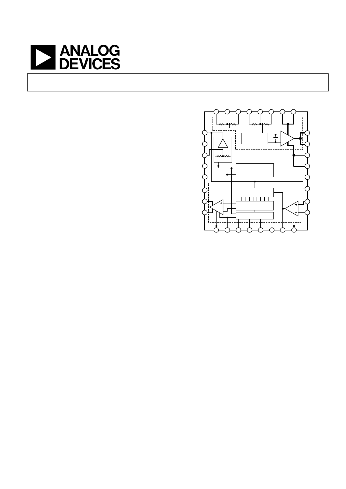
FUNCTIONAL BLOCK DIAGRAM
32
2
3
6
31 30
1.5k 1k
29 28 27 26 25
1k 1.5k
GM
HIGH CURRENT DRIVE R
9
24
23
22
21
VMID
4
1
AD8260
VMDO
TXEN
VMDI
VNCM
VPSB
ENBL
VGAP
VGAN
VNGR VPSR GNS3 GNS2 GNS1 GNS0 PRAO VNGR
V
OCM INPP INRP INRN INPN T XFBVNEGVNEG
TXOP
TXOP
VPOS
VPOS
VPSR
VMDO
PRAI
FDBK
07192-001
5
7
8
10 11 12 13 14 1615
17
18
19
20
BIAS
VGA/PREAMPLIFIER
ATTENUATOR
GM STAGES
LOGIC
×1
+–
Figure 1. Functional Block Diagram
GENERAL DESCRIPTION
The AD8260 includes a high current driver, usable as a
transmitter, and a low noise digitally programmable variable
gain amplifier (DGA), useable as a receiver.
The receiver section consists of a single-ended input preamplifier, and linear-in-dB, differential-output DGA. The receiver has
a small signal –3 dB bandwidth of 230 MHz; the driver small
signal bandwidth is 195 MHz. The driver delivers ±300 mA,
well suited for driving low impedance loads, even when
connected to a 3.3 V supply.
The AD8260 DGA is ideal for trim applications and has a gain
span of 30 dB, in 3 dB steps. Excellent bandwidth uniformity is
maintained across the entire frequency range. The low outputreferred noise of the DGA is advantageous in driving high
speed ADCs. The differential output facilitates the interface to
modern low voltage high speed ADCs.
Single-supply and dual-supply operation makes the part versatile
and enables gain control of negative-going pulses, such as those
generated by photodiodes or photo-multiplier tubes, as well as
processing band-pass signals on a single supply. For maximum
dynamic range, it is essential that the part be ac-coupled when
operating on a single supply.
The AD8260 preamplifier (PrA) is configured with external
resistors for gains greater than 6 dB and can be inverting or
noninverting. The DGA is characterized with a noninverting
preamplifier gain of 2×. The attenuator has a range of 30 dB and
the output amplifier has a gain of 8× (18.06 dB). The lowest
noninverting gain range is −6 dB to +24 dB and shifts up with
increased preamplifier gain. The gain is controlled via a parallel
port (Pin GNS0 to Pin GNS3) with 10 gain steps of 3 dB per
code. The preamplifier and DGA are disabled for any code that
is not assigned a gain step.
The AD8260 can operate with single or dual supplies from 3.3 V
to ±5 V. An internal buffer normally provides a split supply
reference for single-supply operation; an external reference
can also be used when the VMID buffer is shut down.
The operating temperature range is −40°C to +105°C. The
AD8260 is available in a 5 mm × 5 mm, 32-lead LFCSP.

AD8260
Rev. 0 | Page 2 of 32
TABLE OF CONTENTS
Features .............................................................................................. 1
Applications ....................................................................................... 1
Functional Block Diagram .............................................................. 1
General Description ......................................................................... 1
Revision History ............................................................................... 2
Specifications ..................................................................................... 3
Absolute Maximum Ratings ............................................................ 6
ESD Caution .................................................................................. 6
Pin Configuration and Function Descriptions ............................. 7
Typical Performance Characteristics ............................................. 8
Test Circuits ..................................................................................... 16
Theory of Operation ...................................................................... 20
Overview ...................................................................................... 20
High Current Driver Amplifier ................................................ 21
Precautions to Be Observed During Half-Duplex
Operation ..................................................................................... 22
VMID Buffer ............................................................................... 22
Preamplifier ................................................................................. 22
Preamplifier Noise ...................................................................... 22
DGA ............................................................................................. 23
Gain Control ............................................................................... 23
Output Stage ................................................................................ 23
Attenuator.................................................................................... 23
Single-Supply Operation and AC Coupling ........................... 24
Power-Up/Power-Down Sequence .......................................... 24
Logic Interfaces ........................................................................... 24
Applications Information .............................................................. 25
Evaluation Board ............................................................................ 26
Connecting the Evaluation Board ............................................ 27
Outline Dimensions ....................................................................... 32
Ordering Guide .......................................................................... 32
REVISION HISTORY
5/08—Revision 0: Initial Version
AD8260
Rev. 0 | Page 3 of 32
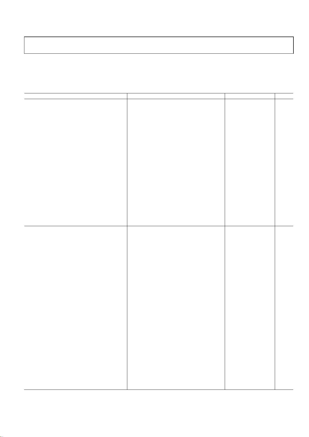
SPECIFICATIONS
VS (supply voltage) = 3.3 V, TA = 25°C, preamplifier gain = 2× (R
FB1
= R
FB2
= 100 Ω), V
VMDO
= VS/2, f = 10 MHz, CL = 5 pF, R
LOAD
= 500 Ω,
DGA differential output. All dBm values are referenced to 50 Ω, gain code 1011, unless otherwise specified.
Table 1.
Parameter Conditions Min Typ Max Unit
DRIVER AMPLIFIER—GENERAL PARAMETERS
–3 dB Small Signal Bandwidth V
OUT
= 10 mV p-p, R
LOAD
= 500 Ω 195 MHz
V
OUT
= 10 mV p-p, R
LOAD
= 50 Ω 120 MHz
V
OUT
= 10 mV p-p, R
LOAD
= 10 Ω 85 MHz
–3 dB Large Signal Bandwidth V
OUT
= 1 V p-p 195 MHz
V
OUT
= 2 V p-p 190 MHz
V
OUT
= 2 V p-p, R
LOAD
= 50 Ω 180 MHz
Slew Rate V
OUT
= 1 V p-p 730 V/µs
V
OUT
= 2 V p-p 725 V/µs
V
OUT
= 2 V p-p, R
LOAD
= 50 Ω 620 V/µs
Gain Nominal gain with internal gain setting resistors 3.0 3.52 dB
Input Voltage Noise f = 10 MHz 9.5 nV/√Hz
Noise Figure RS = 100 Ω (differential, 2 × 50 Ω that convert
differential DAC output currents to differential voltage)
17.6 dB
Output-Referred Noise Gain = 3.52 dB (1.5×), includes internal gain setting
resistors
14.3 nV/√Hz
Output Impedance DC to 10 MHz, VS = ±3.3 V ≤1.7 Ω
Output Current R
LOAD
= 1 Ω, VIN = ±0.5 V ±310 mA
Output Signal Range R
LOAD
≥ 500 Ω V
MDO
± 1.5 V
V
S
= +5 V V
MDO
± 2.3 V
V
S
= ±5 V
±4.7 V
Input Signal Range Differential input signal 2 V p-p
Output Offset Voltage Gain = 3.52 dB (1.5×), max and min limits are 3σ −20 ±5 +20 mV
DRIVER AMPLIFIER—DYNAMIC PERFORMANCE
Harmonic Distortion V
OUT
= 1 V p-p
HD2 f = 1 MHz −84 dBc
HD3 −85 dBc
HD2 f = 10 MHz −83 dBc
HD3 −70 dBc
Harmonic Distortion V
OUT
= 2 V p-p
HD2 f = 1 MHz −78 dBc
HD3 −76 dBc
HD2 f = 10 MHz −70 dBc
HD3 −58 dBc
Input 1 dB Compression Point 13 dBm
Multitone Power Ratio (MTPR, In-Band) R
LOAD
= 50 Ω, V
OUT
= 1.4 V p-p max, 10 tones, 2 MHz to
22 MHz with missing tone at 12 MHz (spacing 2 MHz)
−49 dBc
R
LOAD
= 50 Ω, V
OUT
= 1.4 V p-p max, 16 tones, 2 MHz to
38 MHz with missing tones at 10 MHz, 20 MHz, 30 MHz,
and 40 MHz (spacing 2 MHz)
−43 dBc
Two-Tone Intermodulation Distortion (IMD3) V
OUT
= 1 V p-p, f1 = 10 MHz, f2 = 11 MHz −90 dBc
V
OUT
= 2 V p-p, f1 = 10 MHz, f2 = 11 MHz −71 dBc
V
OUT
= 1 V p-p, f1 = 45 MHz, f2 = 46 MHz −60 dBc
V
OUT
= 2 V p-p, f1 = 45 MHz, f2 = 46 MHz −48 dBc
Output Third-Order Intercept V
OUT
= 1 V p-p, f = 10 MHz 43 dBm
V
OUT
= 2 V p-p, f = 10 MHz 40 dBm
V
OUT
= 1 V p-p, f = 45 MHz 28 dBm
V
OUT
= 2 V p-p, f = 45 MHz 28 dBm
Two-Tone Intermodulation Distortion (IMD3),
R
LOAD
= 50 Ω
V
OUT
= 1 V p-p, f1 = 10 MHz, f2 = 11 MHz −69 dBc
V
OUT
= 2 V p-p, f1 = 10 MHz, f2 = 11 MHz −72 dBc
V
OUT
= 1 V p-p, f1 = 45 MHz, f2 = 46 MHz −51 dBc
V
OUT
= 2 V p-p, f1 = 45 MHz, f2 = 46 MHz −48 dBc
AD8260
Rev. 0 | Page 4 of 32
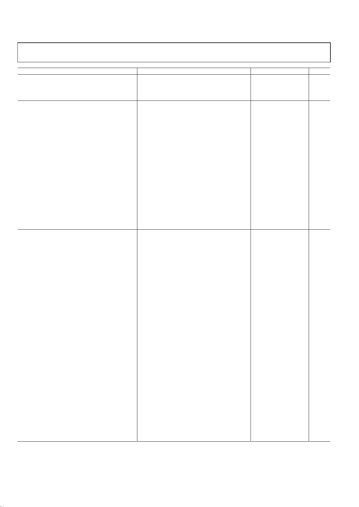
Parameter Conditions Min Typ Max Unit
Output Third-Order Intercept, R
LOAD
= 50 Ω V
OUT
= 1 V p-p, f = 10 MHz 33 dBm
V
OUT
= 2 V p-p, f = 10 MHz 40 dBm
V
OUT
= 1 V p-p, f = 45 MHz 23 dBm
V
OUT
= 2 V p-p, f = 45 MHz 28 dBm
PREAMPLFIER AND VGA—GENERAL PARAMETERS
−3 dB Small Signal Bandwidth V
OUT
= 10 mV p-p, gain code = 0110 230 MHz
−3 dB Large Signal Bandwidth V
OUT
= 1 V p-p, gain code = 0110 165 MHz
V
OUT
= 2 V p-p, gain code = 0110 135 MHz
Slew Rate V
OUT
= 1 V p-p, gain code = 0110 330 V/µs
V
OUT
= 1.6 V p-p, gain code = 0110 335 V/µs
Input Voltage Noise f = 10 MHz (shorted input) 2.4 nV/√Hz
f = 10 MHz (input open) 6.2 nV/√Hz
Noise Figure Max gain (gain code = 1011), RS = 50 Ω, unterminated 10.2 dB
Max gain (gain code = 1011), RS = 50 Ω,
shunt terminated with 50 Ω
15.5 dB
Output-Referred Noise Max gain (gain code = 1011), gain = 24 dB (input short) 38 nV/√Hz
Max gain (gain code = 1011), gain = 24 dB (input open) 98.1 nV/√Hz
Min gain (gain code = 0001), gain = −6 dB 25 nV/√Hz
Output Impedance DC to 10 MHz ≤3 Ω
Output Signal Range (per Pin) R
LOAD
≥ 500 Ω V
MDO
± 0.7 V
V
S
= +5 V V
MDO
± 1.4 V
V
S
= ±5 V ±3.6 V
Input Signal Range Preamplifier input V
MDO
± 0.3 V
Output Offset Voltage Max gain (gain code = 1011), gain = 24 dB, 3 σ limits −50 ±20 +50 mV
PREAMPLIFIER AND VGA—DYNAMIC PERFORMANCE
Harmonic Distortion Gain code = 0110, gain = 9 dB, V
OUT
= 1 V p-p
HD2 f = 1 MHz −90 dBc
HD3 −87 dBc
HD2 f = 10 MHz −75 dBc
HD3 −58 dBc
Harmonic Distortion Gain code = 1011, gain = 24 dB, V
OUT
= 2 V p-p
HD2 f = 1 MHz −94 dBc
HD3 −90 dBc
HD2 f = 10 MHz −61 dBc
HD3 −84 dBc
Input 1 dB Compression Point Min gain (gain code = 0001), gain = −6 dB
(preamplifier limited)
1.9 dBm
Max gain (gain code = 1011), gain = 24 dB
(VGA limited)
−9.2 dBm
MTPR (In-Band) V
OUT
= 1.4 V p-p-max, 10 tones, 2 MHz to 22 MHz with
missing tone at 12 MHz (spacing 2 MHz),
gain code = 1011, gain = 24 dB
−68 dBc
V
OUT
= 1.4 V p-p-max, 16 tones, 2 MHz to 38 MHz with
missing tones at 10 MHz, 20 MHz, 30 MHz, and 40 MHz
(spacing 2 MHz)
−61 dBc
Two-Tone Intermodulation Distortion (IMD3) Gain code = 1011, gain = 24 dB
V
OUT
= 1 V p-p, f1 = 10 MHz, f2 = 11 MHz −92 dBc
V
OUT
= 2 V p-p, f1 = 10 MHz, f2 = 11 MHz −77 dBc
V
OUT
= 1 V p-p, f1 = 45 MHz, f2 = 46 MHz −50 dBc
V
OUT
= 2 V p-p, f1 = 45 MHz, f2 = 46 MHz −36 dBc
Output Third-Order Intercept Gain code = 1011, gain = 24 dB
V
OUT
= 1 V p-p, f = 10 MHz 44 dBm
V
OUT
= 2 V p-p, f = 10 MHz 43 dBm
V
OUT
= 1 V p-p, f = 45 MHz 27 dBm
V
OUT
= 2 V p-p, f = 45 MHz 22 dBm
Overload Recovery Max gain (gain code = 1011), gain = 24 dB,
V
IN
= 50 mV p-p to 500 mV p-p
50 ns
Group Delay Variation 1 MHz < f < 50 MHz, full gain range 2 ns
AD8260
Rev. 0 | Page 5 of 32
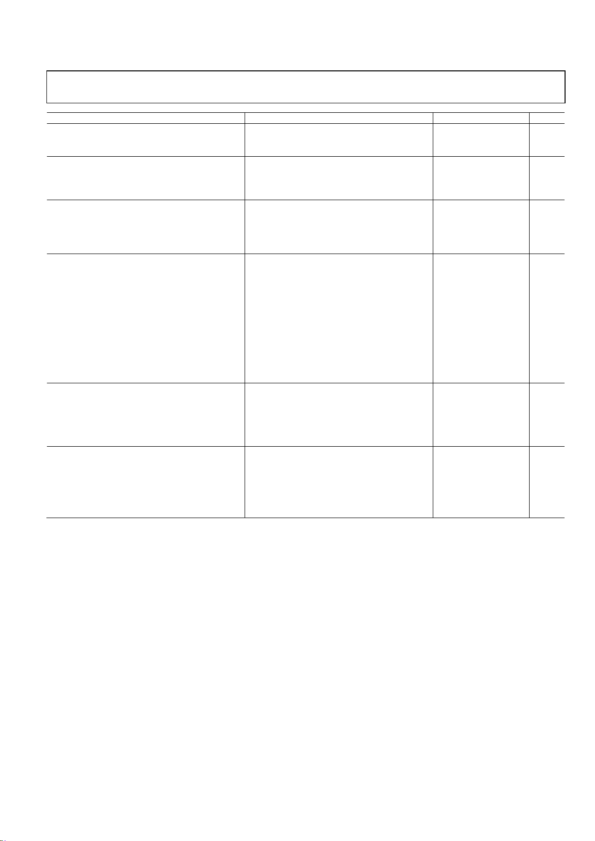
Parameter Conditions Min Typ Max Unit
ACCURACY
Absolute Gain Error All gain codes, limits are 3σ −0.5 ±0.15 +0.5 dB
Gain Law Conformance (DNL) Differential gain error code-to-code −0.3 ±0.15 +0.3 dB
GAIN CONTROL
Gain Step per Code 3.0 dB
Gain Range Default = −6dB to +24 dB 30 dB
Resp onse Tim e 30 dB gain change (gain code stepped from 0001 to 1011) 50 ns
LOGIC INTERFACES
High Level Input Voltage 1.4 V
S
V
Low Level Input Voltage 0 0.8 V
Logic Input Bias Current Logic high, V
LOGIC
= 3.3 V 0.2 A
Logic low 18 nA
POWER SUPPLY
Supply Voltage Single supply 3.3 10 V
Dual supply ±3.3 ±5 V
Quiescen t Curren t Full chip enabled (TXEN = 1, ENBL = 1, gain code = 0001) 28.3 mA
TXEN = 0, ENBL = 1, gain code = 0001, driver off, DGA on 19.1 mA
TXEN = 1, ENBL = 1, gain code = 0000, driver on, DGA off 10.8 mA
Chip disabled (TXEN = 0, ENBL = 0, gain code = 0000) 35 µA
V
S
= ±5 V, no signal 34.2 mA
PSRR Max gain (gain code = 1011), gain = 24 dB, 1 MHz −30 dB
Driver amplifier, 1 MHz −48 dB
Power Dissipation No signal 93 mW
No signal, V
POS
− V
NEG
= 10 V 342 mW
ENABLE TIMES
Chip Enable Time Bias only, TXEN = 0, gain code = 0000, ENBL = 0 to 1 0.4 µs
All at once, TXEN = 0 to 1, gain code = 0000 to 0001,
ENBL = 0 to 1
0.3 µs
Preamplifier and DGA Enable Time ENBL = 1, TXEN = 0, gain code = 0000 to 0001 0.3 µs
Driver Enable Time ENBL = 1, gain code = 0001, TXEN stepped from 0 to 1 0.2 µs
DISABLE TIMES
Chip Disable Time TXEN = 1 to 0, gain code = 0001 to 0000,
ENBL = 1 to 0, I
SUPPLY
= 100 A
20 µs
All at once, TXEN = 1 to 0, gain code = 0001 to 0000,
ENBL = 1 to 0, I
SUPPLY
= 35 µA
50 µs
Preamplifier and DGA Disable Time ENBL = 1, TXEN = 0, gain code = 0001 to 0000 0.4 µs
Driver Disable Time ENBL = 1, gain code = 0000, TXEN = 1 to 0 2.2 µs
AD8260
Rev. 0 | Page 6 of 32
ABSOLUTE MAXIMUM RATINGS
Table 2.
Parameter Rating
Voltage
Supply Voltage (VPOS, VNEG) ±6 V
Input Voltage (INxx, PRAI,
FDBK, VMDI, VOCM)
VPOS, VNEG
Logic Voltages VPOS, ground
Temperature
Operating Temperature Range –40°C to +105°C
Storage Temperature Range –65°C to +150°C
Lead Temperature (Soldering, 60 sec) 300°C
Thermal Data1
Maximum Junction Temperature 125°C
θJA 47.3°C/W
θJC 6.9°C/W
θJB 28.6°C/W
ΨJT 0.6°C/W
ΨJB 27.4°C/W
1
Thermal data at zero airflow with exposed pad soldered to four-layer JEDEC
board with vias per JESD51-5.
Stresses above those listed under Absolute Maximum Ratings
may cause permanent damage to the device. This is a stress
rating only; functional operation of the device at these or any
other conditions above those indicated in the operational
section of this specification is not implied. Exposure to absolute
maximum rating conditions for extended periods may affect
device reliability.
ESD CAUTION
AD8260
Rev. 0 | Page 7 of 32
PIN CONFIGURATION AND FUNCTION DESCRIPTIONS
7192-002
8
7
6
5
1
4
3
2
29303132 28 252627
20
17
18
19
21
22
23
24
VPSR
FDBK
PRAI
VMDO
VPOS
VPOS
TXOP
TXOP
INPN
VNEG
VNEG
TXFB
INRN
INRP
INPP
VOCM
14139121110 15 16
PIN 1
INDICATOR
AD8260
TOP VIEW
(Not to Scale)
VMDO
TXEN
VMDI
VNCM
VPSB
ENBL
VGAP
VGAN
VNGR
VPSR
GNS3
GNS2
GNS1
GNS0
PRAO
VNGR
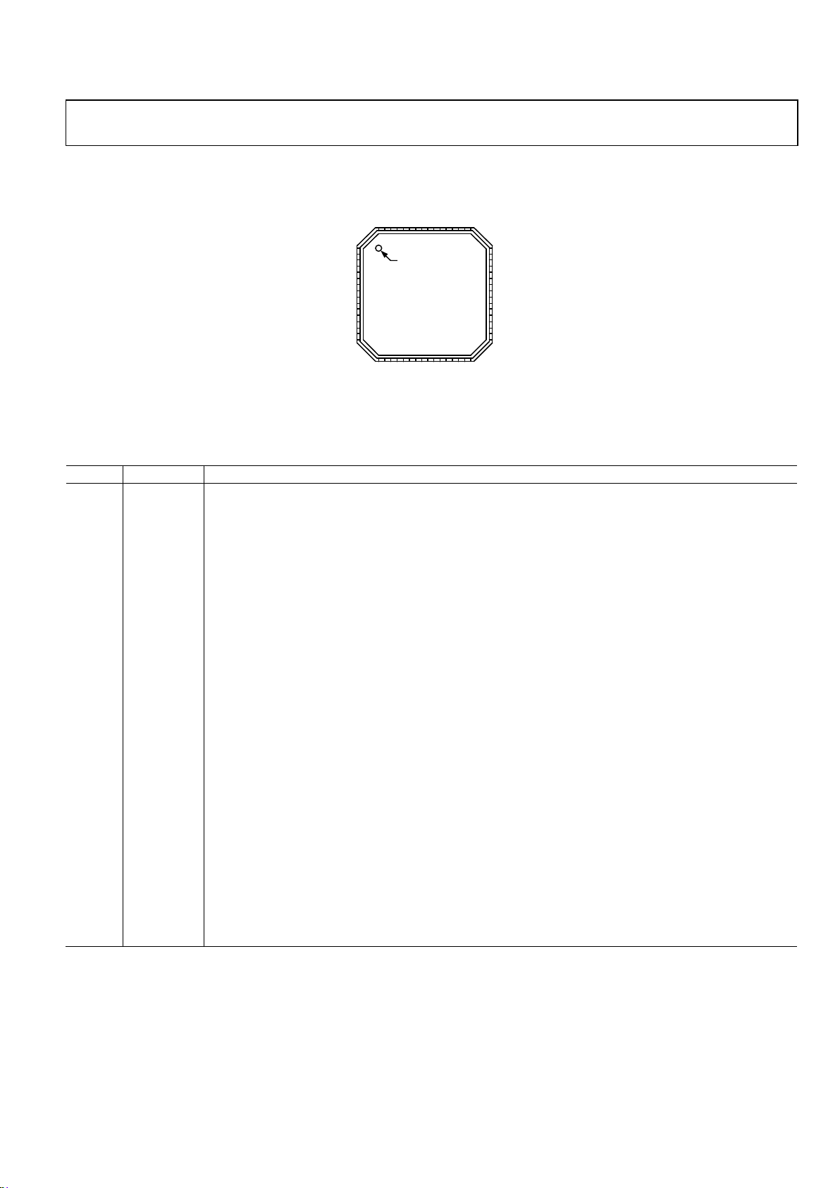
Figure 2. Pin Configuration
Table 3. Pin Function Descriptions
Pin No. Mnemonic Description
1, 191 VMDO VMID Buffer Output. Requires robust ac decoupling with a capacitance of 0.1 µF capacitor or greater.
2 TXEN Driver Enable. Logic threshold = 1.1 V with ±0.2 V hysteresis.
3 VMDI
VMID Input Voltage. Normally decoupled with a 0.1 µF capacitor. When pulled to VNCM, the VMID buffer shuts
down. This can be useful when using the part with dual supplies or when an external midpoint generator is used.
4 VNCM Negative Supply for Bias Cell, VMID Cell, and Logic Inputs. (Ground this pin in applications.)
5 VPSB Positive Supply for Bias Cell and VMID Cell.
6 ENBL
Enable. Logic threshold = 1.1 V. When low, the AD8260 is disabled and the supply current is 35 µA when TXEN
and all GNSx pins are also low.
7 VGAP Positive VGA Output (Needs to Be Ac-Coupled for Single Supply).
8 VGAN Negative VGA Output (Needs to Be Ac-Coupled for Single Supply).
9, 161 VNGR Negative Supply for Preamplifier and DGA (Set to −VPOS for Dual Supply; GND for Single Supply).
10, 201 VPSR Positive Supply for Preamplifier, DGA, and GNSx Logic Decoder.
11 GNS3 MSB for Gain Control. Logic threshold = 1.1 V.
12 GNS2 Gain Control Bit. Logic threshold = 1.1 V.
13 GNS1 Gain Control Bit. Logic threshold = 1.1 V.
14 GNS0 LSB for Gain Control. Logic threshold = 1.1 V.
15 PRAO Preamplifier Output.
17 FDBK Negative Input of Preamplifier.
18 PRAI Positive Input of Preamplifier.
21, 221 VPOS Positive Supply for Driver Amplifier.
23, 241 TXOP Driver Output.
25, 261 VNEG Negative Supply for Driver Amplifier (Set to −VPOS for Dual Supply; GND for Single Supply).
27 TXFB Feedback for Driver Amplifier.
28 INPN Negative Driver Amplifier Input.
29 INRN Negative Gain Resistor Input for Driver Amplifier.
30 INRP Positive Gain Resistor Input for Driver Amplifier.
31 INPP Positive Driver Amplifier Input.
32 VOCM Output Common Mode Pin. Normally connected to Pin VMDO.
1
Pins with the same name are connected internally.
AD8260
Rev. 0 | Page 8 of 32
TYPICAL PERFORMANCE CHARACTERISTICS
VS (supply voltage) = 3.3 V, TA = 25°C, CL = 5 pF, f = 10 MHz, preamplifier gain = 2×, R
FB1
and R
FB2
of the preamplifier = 100 ,
R
LOAD
of the driver amplifier = 500 , TX and RX enabled, unless otherwise specified.
5
1
0
2
3
4
GAIN (dB)
FREQUENCY (Hz)
200M
100M
10M1M100k
T = –40°C
V
OUT
= 200 mV p -p
T = +105° C
07192-003
T= +25°C
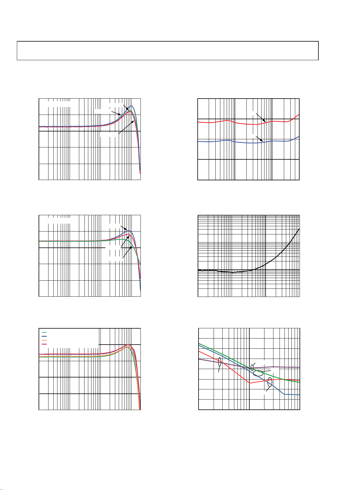
Figure 3. Small-Signal Frequency Response at Three Temperatures of the
High Current Driver—See Figure 51
5
1
0
2
3
4
GAIN (dB)
FREQUENCY (Hz)
200M
100M
10M1M100k
VS = +5V
V
OUT
= 200 mV p -p
VS = +3.3V
VS = ±5V
07192-004
Figure 4. Small-Signal Frequency Response of the High Current Driver for
Three Supply Voltages—See Figure 51
5
1
0
2
3
4
GAIN (dB)
FREQUENCY (Hz)
200M
100M
10M1M100k
07192-005
V
LOAD
= 1V p-p; R
LOAD
=50
V
LOAD
= 1V p-p; R
LOAD
=500
V
LOAD
= 2V p-p; R
LOAD
=50
V
LOAD
= 2V p-p; R
LOAD
=500
Figure 5. Large-Signal Frequency Response of the High Current Driver for Two
Values of Output Voltage and Two Values of Load Resistance—See Fig ure 51
20
0
5
10
15
NOISE (nV/Hz)
FREQUENCY (Hz)
50M10M1M100k
RTO
RTI
07192-006
Figure 6. Input-Referred and Output-Referred Noise of the High Current
Driver—See Figure 52
10
OUTPUT IMP EDANCE ()
FREQUENCY (Hz)
100M10M1M100k
100
0.1
1
7192-007
Figure 7. Output Impedance of the High Current Driver
See Figure 53
– 100
HARMONIC DIST ORTION ( dBc)
LOAD RESISTANCE ()
1k10010
–40
–
20
–60
–80
–90
HD3
HD2
–70
–50
–30
2V p-p
1V p-p
07192-008
Figure 8. Harmonic Distortion (HD2, HD3) vs. Load Resistance for the High
Current Driver—See Figure 54
AD8260
Rev. 0 | Page 9 of 32
–100
HARMONIC DISTORTION (d Bc)
LOAD CAPACITANCE ( pF)
100400
–40
–
20
–60
–80
–90
802010 60
f = 10MHz
–70
–50
–30
50 9030 70
HD2, V
OUT
= 1V p-p
HD3, V
OUT
= 1V p-p
HD2, V
OUT
= 2V p-p
HD3, V
OUT
= 2V p-p
07192-009
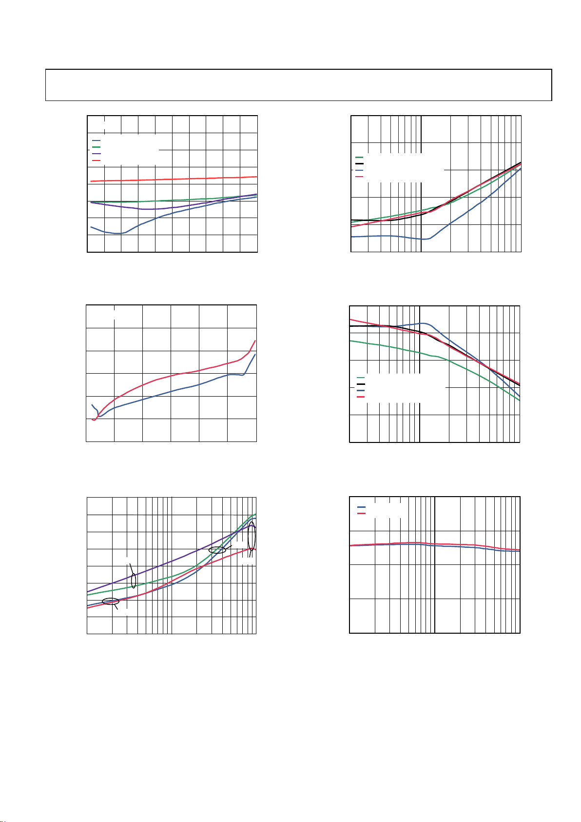
Figure 9. Harmonic Distortion (HD2, HD3) vs. Load Capacitance at Two
Values of Output Voltage for the High Current Driver—See Figure 54
–100
HARMONIC DIST ORTION ( dBc)
OUTPUT VOLTAGE (V p-p)
3.01.50
–40
–20
–60
–80
–120
0
2.51.00.5 2.0
HD3
HD2
f = 10MHz
07192-010
Figure 10. Harmonic Distortion (HD2, HD3) vs. Output Voltage for the High
Current Driver—See Figure 54
–100
HARMONIC DISTORTION (d Bc)
FREQUEN CY (Hz)
100M10M
1M
–40
–
20
–60
–80
–90
HD3
HD2
–70
–50
–30
1V p-p
2V p-p
07192-011
Figure 11. Harmonic Distortion (HD2, HD3) vs. Frequency of the High Current
Driver at Two Values of Output Voltage—See Figure 54
100M
FREQUENCY (Hz)
2M
IMD3 (dBc)
10M
–100
–80
–60
–40
–20
0
R
LOAD
= 50, V
OUT
= 1V p-p
R
LOAD
= 50, V
OUT
= 2V p-p
R
LOAD
= 500, V
OUT
= 1V p-p
R
LOAD
= 500, V
OUT
= 2V p-p
07192-012
Figure 12. IMD3 vs. Frequency for Two Values of Output Voltage and Two
Values of Load Resistance for the High Current Driver—See Figure 55
100M
FREQUENCY (Hz)
2M
OIP3 (dBm)
10M
50
40
30
20
10
0
R
LOAD
= 50, V
OUT
= 1V p-p
R
LOAD
= 50, V
OUT
= 2V p-p
R
LOAD
= 500, V
OUT
= 1V p-p
R
LOAD
= 500, V
OUT
= 2V p-p
07192-013
Figure 13. Third-Order Intercept (OIP3) vs. Frequency for the High Current Driver
See Figure 55
0
20
IP1dB (dBm)
FREQUENCY (Hz)
100M10M1M
5
15
10
R
LOAD
= 50
R
LOAD
= 500
07192-014
Figure 14. Input-Referred 1 dB Compression (IP1dB) vs. Frequency for Two
Values of Load Resistance for the High Current Driver
AD8260
Rev. 0 | Page 10 of 32
–80
FREQUENCY (MHz)
24221821006124201614
0
8
OUTPUT (d Bm)
–60
–40
–90
–70
–20
–50
–30
–10
07192-015
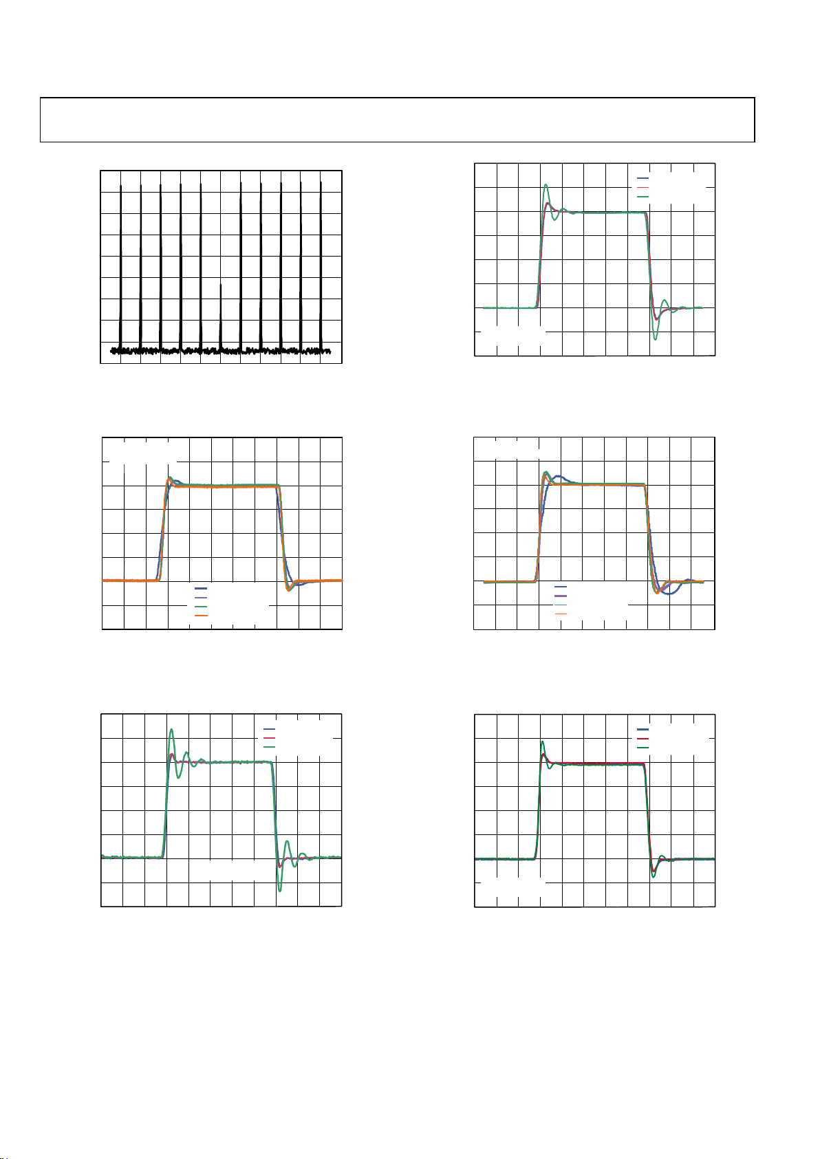
Figure 15. Missing Tone Power Ratio for the High Current Driver
0
0.15
–0.15
0 .05
0.10
OUTPUT VOL TAGE (V)
TIME (ns)
807060
–0.05
–0.10
–20 10–30 0 30–10 20 5040
–0.20
0.20
R
LOAD
= 10
R
LOAD
= 50
R
LOAD
= 100
R
LOAD
= 500
C
LOAD
= 5pF
NONINVE RTING
07192-016
Figure 16. Small-Signal Pulse Resp onse of the High Current Driver for Various
Values of Load Resistance, R
LOAD
—See Figure 56
0
0.15
–0.15
0.05
0.10
OUTPUT VOLTAGE (V)
TIME (ns)
807060
–0.05
–0.10
–20 10–30 0 30–10 20 5040
–0.20
0.20
C
LOAD
= 5pF
C
LOAD
= 47pF
C
LOAD
= 10pF
R
LOAD
= 500
NONINVERTING
07192-017
Figure 17. Small-Signal Pulse Resp onse of the High Current Driver for Various
Values of Load Capacitance, C
LOAD
, and R
LOAD
= 500 Ω—See Figure 56
0
0.15
–0.15
0.05
0.10
OUTPUT VOLTAGE (V)
TIME (ns)
807060
–0.05
–0.10
–20 10–30 0 30–10 20 5040
–0.20
0.20
C
LOAD
= 5pF
C
LOAD
= 47pF
C
LOAD
= 10pF
R
LOAD
= 50
NONINVERTI NG
07192-018
Figure 18. Small-Signal Pulse Resp onse of the High Current Driver for Various
Values of Load Capacitance, C
LOAD
, and 50 Ω Load—See Figure 56
OUTPUT VOLT AGE (V)
TIME (ns)
80706020 1030 0 3010 20 5040
2.0
1.5
1.0
0.5
0
–0.5
–1.0
–1.5
–2.0
R
LOAD
=10
R
LOAD
= 50
R
LOAD
=100
R
LOAD
= 500
C
LOAD
=5pF
NONINVERTI NG
07192-019
Figure 19. Large-Signal Pulse Response of the High Current Driver for Various
Values of Load Resistance, R
LOAD
—See Figure 56
0
1.5
–1.5
0.5
1.0
OUTPUT VOLTAGE (V)
TIME (ns)
807060
–0.5
–1.0
–20 10–30 0 30–10 20 5040
–2.0
2.0
C
LOAD
= 5pF
C
LOAD
= 47pF
C
LOAD
= 10pF
R
LOAD
= 500
NONINVERTING
07192-020
Figure 20. Large-Signal Pulse Response of the High Current Driver for Various
Values of Load Capacitance, C
LOAD
, and R
LOAD
= 500 Ω—See Figure 56
 Loading...