Analog Devices ADF4216 7 8 Datasheet
a
Dual RF PLL Frequency Synthesizers
ADF4216/ADF4217/ADF4218
FEATURES
ADF4216: 550 MHz/1.2 GHz
ADF4217: 550 MHz/2.0 GHz
ADF4218: 550 MHz/2.5 GHz
2.7 V to 5.5 V Power Supply
Selectable Charge Pump Currents
Selectable Dual Modulus Prescaler
IF: 8/9 or 16/17
RF: 32/33 or 64/65
3-Wire Serial Interface
Power-Down Mode
APPLICATIONS
Wireless Handsets (GSM, PCS, DCS, CDMA, WCDMA)
Base Stations for Wireless Radio (GSM, PCS, DCS,
CDMA, WCDMA)
Wireless LANS
Communications Test Equipment
CATV Equipment
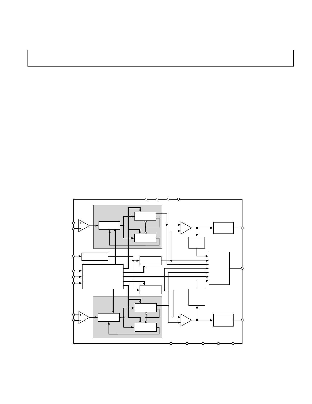
FUNCTIONAL BLOCK DIAGRAM
VDD1VDD2VP1VP2
N = BP + A
11-BIT IF
IF
A
IN
B
IF
IN
IF
PRESCALER
B-COUNTER
6-BIT IF
A-COUNTER
GENERAL DESCRIPTION
The ADF4216/ADF4217/ADF4218 are dual frequency synthesizers that can be used to implement local oscillators (LOs) in
the upconversion and downconversion sections of wireless
receivers and transmitters. They can provide the LO for both
the RF and IF sections. They consist of a low-noise digital PFD
(Phase Frequency Detector), a precision charge pump, a programmable reference divider, programmable A and B counters,
and a dual-modulus prescaler (P/P+1). The A (6-bit) and B
(11-bit) counters, in conjunction with the dual modulus prescaler
(P/P+1), implement an N divider (N = BP + A). In addition,
the 14-bit reference counter (R Counter), allows selectable
REFIN frequencies at the PFD input. A complete PLL (PhaseLocked Loop) can be implemented if the synthesizers are
used with an external loop filter and VCOs (Voltage Controlled Oscillators).
Control of all the on-chip registers is via a simple 3-wire interface.
The devices operate with a power supply ranging from 2.7 V
to 5.5 V and can be powered down when not in use.
ADF4216/ADF4217/ADF4218
PHASE
COMPARATOR
IF
LOCK
DETECT
CHARGE
PUMP
CP
IF
REF
CLOCK
DATA
RF
IN
RFINB
IN
LE
A
OSCILLATOR
22-BIT
DATA
REGISTER
N = BP + A
PRESCALER
SDOUT
RF
14-BIT IF
R-COUNTER
14-BIT IF
R-COUNTER
11-BIT RF
B-COUNTER
6-BIT RF
A-COUNTER
REV. 0
Information furnished by Analog Devices is believed to be accurate and
reliable. However, no responsibility is assumed by Analog Devices for its
use, nor for any infringements of patents or other rights of third parties
which may result from its use. No license is granted by implication or
otherwise under any patent or patent rights of Analog Devices.
OUTPUT
MUX
RF
LOCK
DETECT
CHARGE
PUMP
PHASE
COMPARATOR
DGND
One Technology Way, P.O. Box 9106, Norwood, MA 02062-9106, U.S.A.
Tel: 781/329-4700 World Wide Web Site: http://www.analog.com
Fax: 781/326-8703 © Analog Devices, Inc., 2000
AGND
RF
DGND
RF
IF
DGND
AGND
IF
IF
MUXOUT
CP
RF

1
ADF4216/ADF4217/ADF4218–SPECIFICATIONS
VDD1, VDD2 ⱕ VP1, VP2 ⱕ 6.0 V ; AGNDRF = DGNDRF = AGNDIF = DGNDIF = 0 V; TA = T
DD
2
Unit Test Conditions/Comments
DD
DD
V min
V max
1
P
arameter B Version B Chips
RF/IF CHARACTERISTICS (3 V)
RF Input Frequency (RF
) See Figure 3 for Input Circuit.
IN
ADF4216 0.2/1.2 0.2/1.2 GHz min/max For lower frequency operation (below the
ADF4217 0.2/2.0 0.2/2.0 GHz min/max minimum stated) use a square wave source.
ADF4218 0.5/2.5 0.5/2.5 GHz min/max
IF Input Frequency (IF
) 45/550 45/550 MHz min/max
IN
RF Input Sensitivity –15/+4 –15/+4 dBm min/max
IF Input Sensitivity –10/+4 –10/+4 dBm min/max
Maximum Allowable
Prescaler Output Frequency
3
165 165 MHz max
RF/IF CHARACTERISTICS (5 V)
RF Input Frequency (RF
) See Figure 3 for Input Circuit.
IN
ADF4216 0.2/1.2 0.2/1.2 GHz min/max For lower frequency operation (below the
ADF4217 0.2/2.0 0.2/2.0 GHz min/max minimum stated) use a square wave source.
ADF4218 0.5/2.5 0.5/2.5 GHz min/max
IF Input Frequency (IF
) 25/550 25/550 MHz min/max
IN
RF Input Sensitivity –15/+4 –15/+4 dBm min/max
IF Input Sensitivity –10/+4 –10/+4 dBm min/max
Maximum Allowable
Prescaler Output Frequency
3
200 200 MHz max
REFIN CHARACTERISTICS
REFIN Input Frequency 5/40 5/40 MHz min/max For f < 5 MHz, use dc-coupled square wave
REFIN Input Sensitivity
4
0.5 0.5 V p-p min AC-Coupled. When DC-Coupled:
REFIN Input Capacitance 10 10 pF max
REFIN Input Current ± 100 ±100 µA max
PHASE DETECTOR
Phase Detector Frequency
5
40 40 MHz max
CHARGE PUMP
I
Sink/Source
CP
High Value 4.5 4.5 mA typ
Low Value 1.125 1.125 mA typ
Absolute Accuracy 1 1 % typ
I
Three-State Leakage Current 1 1 nA typ
CP
Sink and Source Current Matching 1 1 % typ
I
CP
vs. V
CP
10 10 % max 0.5 V ⱕ VCP ⱕ VP – 0.5 V
ICP vs. Temperature 10 10 % typ VCP = VP/2
LOGIC INPUTS
V
, Input High Voltage 0.8 × V
INH
V
, Input Low Voltage 0.2 × V
INL
I
, Input Current ± 1 ± 1 µA max
INH/IINL
C
, Input Capacitance 10 10 pF max
IN
DD
DD
0.8 × V
0.2 × V
Oscillator Input Current ± 100 ±100 µA max
LOGIC OUTPUTS
V
, Output High Voltage VDD – 0.4 VDD – 0.4 V min IOH = 500 µA
OH
VOL, Output Low Voltage 0.4 0.4 V max IOL = 500 µA
POWER SUPPLIES
V
1 2.7/5.5 2.7/5.5 V min/V max
DD
V
2V
DD
V
P
1V
DD
VDD1/6.0 VDD1/6.0 V min/V max AVDD ⱕ VP ⱕ 6.0 V
MIN
to T
unless otherwise noted.)
MAX
(VDD1 = VDD2 = 3 V ⴞ 10%, 5 V ⴞ 10%;
(0 to V
0 to V
).
DD
max (CMOS-Compatible)
DD
–2–
REV. 0
ADF4216/ADF4217/ADF4218
Parameter B Version B Chips2Unit Test Conditions/Comments
POWER SUPPLIES (Continued)
I
(RF + IF)
DD
ADF4216 18 9 mA max 9.0 mA typical at V
ADF4217 21 12 mA max 12 mA typical at V
ADF4218 25 14 mA max 14 mA typical at V
(RF Only)
I
DD
ADF4216 10 5 mA max 5.0 mA typical at V
ADF4217 14 7 mA max 7.0 mA typical at V
ADF4218 18 9 mA max 9.0 mA typical at V
I
(IF Only)
DD
ADF4216 9 4.5 mA max 4.5 mA typical at V
ADF4217 9 4.5 mA max 4.5 mA typical at V
ADF4218 9 4.5 mA max 4.5 mA typical at V
I
1 + IP2) 0.6 0.6 mA max TA = 25°C
P (IP
Low-Power Sleep Mode 5 5 µA max 0.5 µA typical
NOISE CHARACTERISTICS
Phase Noise Floor
Phase Noise Performance
ADF4216, ADF4217, ADF4218 (IF)
ADF4216 (RF): 900 MHz Output
ADF4217 (RF): 900 MHz Output
ADF4218 (RF): 900 MHz Output
ADF4216 (RF): 836 MHz Output
ADF4217 (RF): 1750 MHz Output
ADF4217 (RF): 1750 MHz Output
ADF4218 (RF): 1960 MHz Output
Spurious Signals
ADF4216 ADF4217, ADF4218 (IF)
ADF4216 (RF): 900 MHz Output
ADF4217 (RF): 900 MHz Output
ADF4218 (RF): 900 MHz Output
ADF4216 (RF): 836 MHz Output
ADF4217 (RF): 1750 MHz Output
ADF4217 (RF): 1750 MHz Output
ADF4218 (RF): 1960 MHz Output14–80/–84 –80/–84 dB typ @ 200 kHz/400 kHz and 200 kHz PFD Frequency
NOTES
1
Operating temperature range is as follows: B Version: –40°C to +85°C.
2
The B Chip specifications are given as typical values.
3
This is the maximum operating frequency of the CMOS counters. The prescaler value should be chosen to ensure that the IF/RF input is divided down to a frequency that is
less than this value.
4
VDD1 = VDD2 = 3 V; For VDD1 = VDD2 = 5 V, use CMOS-compatible levels.
5
Guaranteed by design. Sample tested to ensure compliance.
6
P = 16; RFIN = 900 MHz; IFIN = 540 MHz.
7
The synthesizer phase noise floor is estimated by measuring the in-band phase noise at the output of the VCO and subtracting 20 logN (where N is the N divider value).
8
The phase noise is measured with the EVAL-ADF421XEB1 Evaluation Board and the HP8562E Spectrum Analyzer. The spectrum analyzer provides the REFIN for the
synthesizer (f
9
f
= 10 MHz; f
REFIN
10
f
= 10 MHz; f
REFIN
11
f
= 10 MHz; f
REFIN
12
f
= 10 MHz; f
REFIN
13
f
= 10 MHz; f
REFIN
14
f
= 10 MHz; f
REFIN
Specifications subject to change without notice.
6
7
8
= 10 MHz @ 0 dBm).
REFOUT
= 200 kHz; Offset frequency = 1 kHz; fIF = 540 MHz; N = 2700; Loop B/W = 20 kHz.
PFD
= 200 kHz; Offset frequency = 1 kHz; fRF = 900 MHz; N = 4500; Loop B/W = 20 kHz.
PFD
= 30 kHz; Offset frequency = 300 Hz; fRF = 836 MHz; N = 27867; Loop B/W = 3 kHz.
PFD
= 200 kHz; Offset frequency = 1 kHz; fRF = 1750 MHz; N = 8750; Loop B/W = 20 kHz.
PFD
= 10 kHz; Offset frequency = 200 Hz; fRF = 1750 MHz; N = 175000; Loop B/W = 1 kHz.
PFD
= 200 kHz; Offset frequency = 1 kHz; fRF = 1960 MHz; N = 9800; Loop B/W = 20 kHz.
PFD
–171 –171 dBc/Hz typ @ 25 kHz PFD Frequency
–164 –164 dBc/Hz typ @ 200 kHz PFD Frequency
9
–91 –91 dBc/Hz typ @ 1 kHz Offset and 200 kHz PFD Frequency
10
–87 –87 dBc/Hz typ @ 1 kHz Offset and 200 kHz PFD Frequency
10
–88 –88 dBc/Hz typ @ 1 kHz Offset and 200 kHz PFD Frequency
10
–90 –90 dBc/Hz typ @ 1 kHz Offset and 200 kHz PFD Frequency
11
–78 –78 dBc/Hz typ @ 300 Hz Offset and 30 kHz PFD Frequency
12
–85 –85 dBc/Hz typ @ 1 kHz Offset and 200 kHz PFD Frequency
13
–66 –66 dBc/Hz typ @ 200 Hz Offset and 10 kHz PFD Frequency
14
–84 –84 dBc/Hz typ @ 1 kHz Offset and 200 kHz PFD Frequency
9
–97/–106 –97/–106 dB typ @ 200 kHz/400 kHz and 200 kHz PFD Frequency
10
–98/–106 –98/–106 dB typ @ 200 kHz/400 kHz and 200 kHz PFD Frequency
10
–91/–100 –91/–100 dB typ @ 200 kHz/400 kHz and 200 kHz PFD Frequency
10
–80/–84 –80/–84 dB typ @ 200 kHz/400 kHz and 200 kHz PFD Frequency
11
–80/–84 –80/–84 dB typ @ 30 kHz/60 kHz and 30 kHz PFD Frequency
12
–88/–90 –88/–90 dB typ @ 200 kHz/400 kHz and 200 kHz PFD Frequency
13
–65/–73 –65/–73 dB typ @ 10 kHz/20 kHz and 10 kHz PFD Frequency
See TPC 22 and TPC 23
= 3 V and TA = 25°C
DD
= 3 V and TA = 25°C
DD
= 3 V and TA = 25°C
DD
= 3 V and TA = 25°C
DD
= 3 V and TA = 25°C
DD
= 3 V and TA = 25°C
DD
= 3 V and TA = 25°C
DD
= 3 V and TA = 25°C
DD
= 3 V and TA = 25°C
DD
@ VCO Output
REV. 0
–3–
ADF4216/ADF4217/ADF4218
(VDD1 = VDD2 = 3 V ⴞ 10%, 5 V ⴞ 10%; VP1, VP2 = V
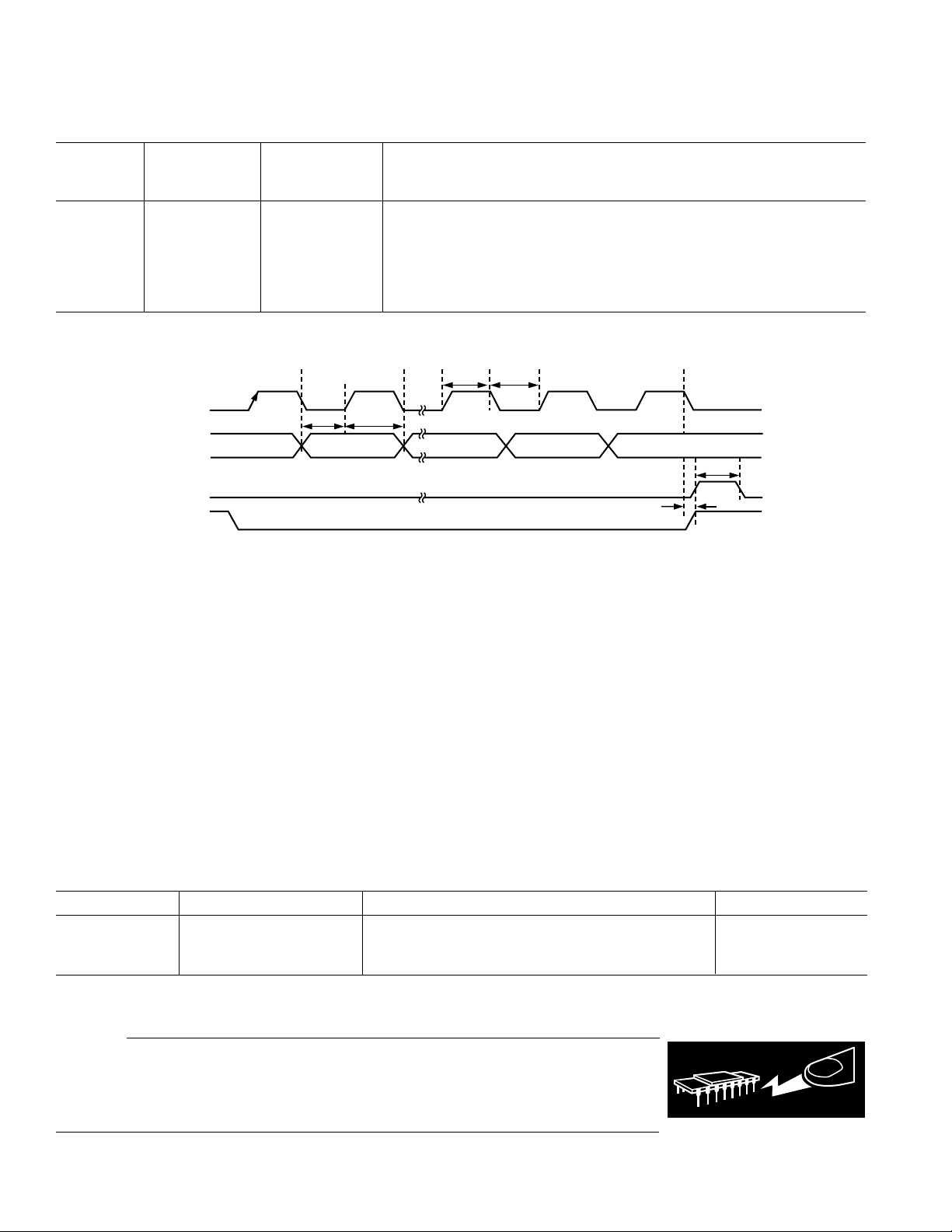
TIMING CHARACTERISTICS
TA = T
Limit at
T
to T
MIN
MAX
Parameter (B Version) Unit Test Conditions/Comments
t
1
t
2
t
3
t
4
t
5
t
6
NOTES
Guaranteed by design but not production tested.
Specification subject to change without notice.
10 ns min DATA to CLOCK Setup Time
10 ns min DATA to CLOCK Hold Time
25 ns min CLOCK High Duration
25 ns min CLOCK Low Duration
10 ns min CLOCK to LE Setup Time
20 ns min LE Pulsewidth
CLOCK
DATA
DB21 (MSB)
LE
LE
to T
MIN
t
1
DB20
unless otherwise noted.)
MAX
t
3
t
2
DB2
t
4
DB1
(CONTROL BIT C2)
5 V ⴞ 10%; AGND = DGND = 0 V;
DD ,
DB0 (LSB)
(CONTROL BIT C1)
t
5
t
6
Figure 1. Timing Diagram
ABSOLUTE MAXIMUM RATINGS
(TA = 25°C unless otherwise noted)
1, 2
VDD1 to GND3 . . . . . . . . . . . . . . . . . . . . . . . . –0.3 V to +7 V
V
1 to VDD2 . . . . . . . . . . . . . . . . . . . . . . . –0.3 V to +0.3 V
DD
V
1, VP2 to GND . . . . . . . . . . . . . . . . . . . . . . –0.3 V to +7 V
P
1, VP2 to VDD1 . . . . . . . . . . . . . . . . . . . . –0.3 V to +5.5 V
V
P
Digital I/O Voltage to GND . . . . . . –0.3 V to DV
Analog I/O Voltage to GND . . . . . . . . . –0.3 V to V
, RFINA, RFINB,
REF
IN
IF
A, IFINB to GND . . . . . . . . . . . –0.3 V to VDD + 0.3 V
IN
+ 0.3 V
DD
+ 0.3 V
P
Operating Temperature Range
Industrial (B Version) . . . . . . . . . . . . . . . . –40°C to +85°C
Storage Temperature Range . . . . . . . . . . . . –65°C to +150°C
Maximum Junction Temperature . . . . . . . . . . . . . . . . 150°C
TSSOP θ
Thermal Impedance . . . . . . . . . . . . . 150.4°C/W
JA
Lead Temperature, Soldering
Vapor Phase (60 sec) . . . . . . . . . . . . . . . . . . . . . . . . 215°C
Infrared (15 sec) . . . . . . . . . . . . . . . . . . . . . . . . . . . . 220°C
NOTES
1
Stresses above those listed under Absolute Maximum Ratings may cause perma-
nent damage to the device. This is a stress rating only; functional operation of the
device at these or any other conditions above those listed in the operational
sections of this specification is not implied. Exposure to absolute maximum rating
conditions for extended periods may affect device reliability.
2
This device is a high-performance RF integrated circuit with an ESD rating of
< 2 kV and it is ESD sensitive. Proper precautions should be taken for handling
and assembly.
3
GND = AGND = DGND = 0 V.
TRANSISTOR COUNT
11749 (CMOS) and 522 (Bipolar).
ORDERING GUIDE
Model Temperature Range Package Description Package Option*
ADF4216BRU –40°C to +85°C Thin Shrink Small Outline Package (TSSOP) RU-20
ADF4217BRU –40°C to +85°C Thin Shrink Small Outline Package (TSSOP) RU-20
ADF4218BRU –40°C to +85°C Thin Shrink Small Outline Package (TSSOP) RU-20
*Contact the factory for chip availability.
CAUTION
ESD (electrostatic discharge) sensitive device. Electrostatic charges as high as 4000 V readily
accumulate on the human body and test equipment and can discharge without detection. Although
the ADF4216/ADF4217/ADF4218 features proprietary ESD protection circuitry, permanent
damage may occur on devices subjected to high-energy electrostatic discharges. Therefore, proper
ESD precautions are recommended to avoid performance degradation or loss of functionality.
–4–
WARNING!
ESD SENSITIVE DEVICE
REV. 0
ADF4216/ADF4217/ADF4218
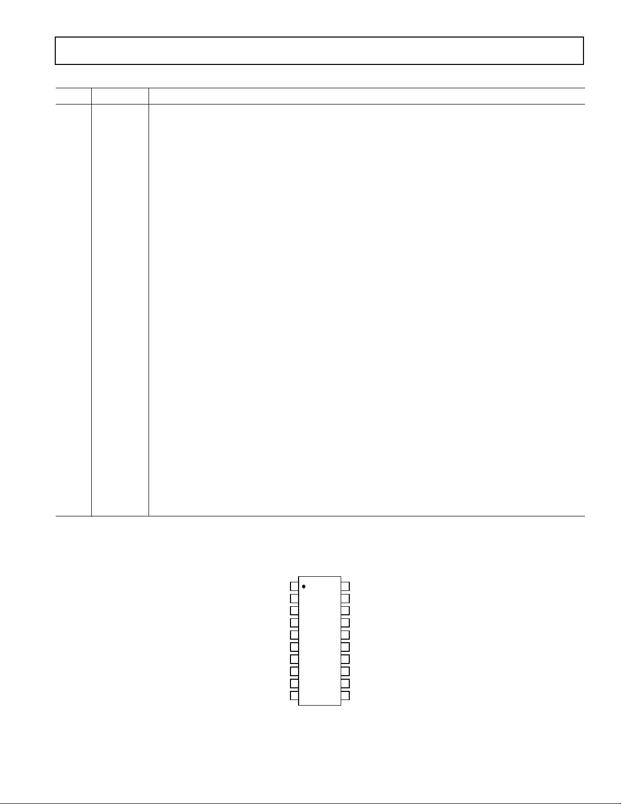
PIN FUNCTION DESCRIPTIONS
Pin No. Mnemonic Function
1V
2V
3CP
4 DGND
5RF
6RF
7 AGND
8 REF
9 DGND
10 MUXOUT This multiplexer output allows either the IF/RF lock detect, the scaled RF, or the scaled Reference Fre-
11 CLK Serial Clock Input. This serial clock is used to clock in the serial data to the registers. The data is latched
12 DATA Serial Data Input. The serial data is loaded MSB first with the two LSBs being the control bits. This input is
13 LE Load Enable, CMOS Input. When LE goes high, the data stored in the shift registers is loaded into one of
14 AGND
15 IF
16 IF
17 DGND
18 CP
19 V
20 V
1 Positive Power Supply for the RF Section. Decoupling capacitors to the analog ground plane should be
DD
placed as close as possible to this pin. V
have the same potential as V
1 Power Supply for the RF Charge Pump. This should be greater than or equal to VDD.
P
RF
Output from the RF Charge Pump. When enabled this provides ±ICP to the external loop filter, which in
DD
2.
1 should have a value of between 2.7 V and 5.5 V. VDD1 must
DD
turn drives the external VCO.
Ground Pin for the RF Digital Circuitry.
RF
A Input to the RF Prescaler. This low-level input signal is normally ac-coupled to the external VCO.
IN
B Complementary Input to the RF Prescaler. This point should be decoupled to the ground plane with a small
IN
bypass capacitor, typically 100 pF.
Ground Pin for the RF Analog Circuitry.
RF
IN
Reference Input. This is a CMOS input with a nominal threshold of VDD/2 and an equivalent input resistance of 100 kΩ. This input can be driven from a TTL or CMOS crystal oscillator or it can be ac-coupled.
Ground Pin for the IF Digital (Interface and Control Circuitry).
IF
quency to be accessed externally. See Table V.
into the 22-bit shift register on the CLK rising edge. This input is a high impedance CMOS input.
a high impedance CMOS input.
the four latches, the latch being selected using the control bits.
Ground Pin for the IF Analog Circuitry.
IF
B Complementary Input to the IF Prescaler. This point should be decoupled to the ground plane with a small
IN
bypass capacitor, typically 100 pF.
A Input to the IF Prescaler. This low-level input signal is normally ac-coupled to the external VCO.
IN
Ground Pin for the IF Digital, Interface, and Control Circuitry.
IF
IF
Output from the IF Charge Pump. When enabled this provides ±ICP to the external loop filter, which in turn
drives the external VCO.
2 Power Supply for the IF Charge Pump. This should be greater than or equal to VDD.
P
2 Positive Power Supply for the IF, Interface, and Oscillator Sections. Decoupling capacitors to the analog
DD
ground plane should be placed as close as possible to this pin. V
2 should have a value of between 2.7 V
DD
and 5.5 V. VDD2 must have the same potential as VDD1.
REV. 0
PIN CONFIGURATION
1
V
DD
V
CP
DGND
RF
IN
RFINB
AGND
REF
DGND
MUXOUT
1
P
RF
RF
A
RF
IN
IF
1
2
3
4
TSSOP
5
ADF4216/
6
ADF4217/
7
ADF4218
8
9
10
VDD2
20
VP2
19
CP
18
DGND
17
IFINA
16
IFINB
15
AGND
14
13
LE
12
DATA
11
CLK
–5–
IF
IF
IF
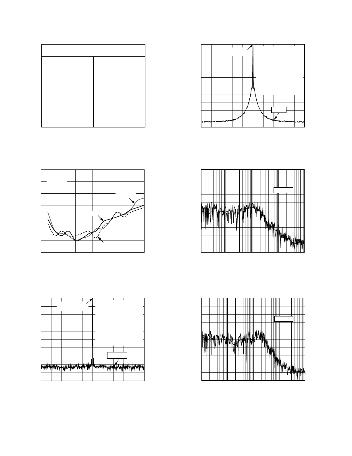
ADF4216/ADF4217/ADF4218
10dB/DIVISION RL = –40dBc/Hz RMS NOISE = 0.65ⴗ
100Hz FREQUENCY OFFSET FROM 900MHz CARRIER 1MHz
0.65ⴗ rms
PHASE NOISE – dBc/Hz
–90
–80
–70
–60
–50
–40
–100
–110
–120
–130
–140
–Typical Performance Characteristics
FREQ-UNIT PARAM-TYPE DATA-FORMAT KEYWORD IMPEDANCE – OHMS
GHz S MA R 50
FREQ MAGS11 ANGS11
0.0 0.957111193 –3.130429321
0.15 0.963546793 –6.686426265
0.25 0.953621785 –11.19913586
0.35 0.953757706 –15.35637483
0.45 0.929831379 –20.3793432
0.55 0.908459709 –22.69144845
0.65 0.897303634 –27.07001443
0.75 0.876862863 –31.32240763
0.85 0.849338092 –33.68058163
0.95 0.858403269 –38.57674885
1.05 0.841888714 –41.48606772
1.15 0.840354983 –45.97597958
1.25 0.822165839 –49.19163116
FREQ MAGS11 ANGS11
1.35 0.816886959 –51.80711782
1.45 0.825983016 –56.20373378
1.55 0.791737125 –61.21554647
1.65 0.770543186 –61.88187496
1.75 0.793897072 –65.39516615
1.85 0.745765233 –69.24884474
1.95 0.7517547 –71.21608147
2.05 0.745594889 –75.93169947
2.15 0.713387801 –78.8391674
2.25 0.711578577 –81.71934806
2.35 0.698487131 –85.49067481
2.45 0.669871818 –88.41958754
2.55 0.668353367 –91.70921678
TPC 1. S-Parameter Data for the AD4218 RF Input
(Up to 2.5 GHz)
0
VDD = 3.3V
= 3.3V
V
P
–5
–10
–15
–20
–25
RF INPUT POWER – dBm
–30
–35
TA = –40ⴗC
TA = +25ⴗC
0
0.5
RF INPUT FREQUENCY – GHz
1.5
1
2
TA = +85ⴗC
2.5
3
TPC 2. Input Sensitivity for the ADF4218 (RF)
–10
–20
–30
–40
–50
–60
–70
OUTPUT POWER – dB
–80
–90
–100
0
REFERENCE
LEVEL = –4.2dBm
–400kHz –200kHz 900MHz +200kHz +400kHz
VDD = 3V, VP = 5V
ICP = 4.375mA
PFD FREQUENCY = 200kHz
LOOP BANDWIDTH = 20kHz
RES. BANDWIDTH = 1kHz
VIDEO BANDWIDTH = 1kHz
SWEEP = 2.5 SECONDS
AVERAGES = 30
–90dBc
TPC 4. ADF4218 RF Reference Spurs (900 MHz, 200 kHz,
20 kHz)
10dB/DIVISION RL = –40dBc/Hz RMS NOISE = 0.55ⴗ
–40
–50
–60
–70
–80
–90
–100
–110
PHASE NOISE – dBc/Hz
–120
–130
–140
100Hz FREQUENCY OFFSET FROM 900MHz CARRIER 1MHz
0.55ⴗ rms
TPC 5. ADF4218 RF Integrated Phase Noise (900 MHz,
200 kHz, 20 kHz)
0
–10
–20
–30
–40
–50
–60
–70
OUTPUT POWER – dB
–80
–90
–100
TPC 3. ADF4218 RF Phase Noise (900 MHz, 200 kHz, 20 kHz)
REFERENCE
LEVEL = –4.2dBm
–2kHz –1kHz 900MHz +1kHz +2kHz
VDD = 3V, VP = 5V
ICP = 4.375mA
PFD FREQUENCY = 200kHz
LOOP BANDWIDTH = 20kHz
RES. BANDWIDTH = 10Hz
VIDEO BANDWIDTH = 10Hz
SWEEP = 1.9 SECONDS
AVERAGES = 19
–90dBc/Hz
TPC 6. ADF4218 RF Integrated Phase Noise (900 MHz,
200 kHz, 35 kHz)
–6–
REV. 0
 Loading...