Direct Modulation/Waveform Generating,
6.1 GHz Fractional-N Frequency Synthesizer
ADF4158
Rev. D
Information furnished by Analog Devices is believed to be accurate and reliable. However, no
Trademarks and registered trademarks are the property of their respective owners.
Fax: 781.461.3113 ©2010–2012 Analog Devices, Inc. All rights reserved.
LOCK
DETECT
N-COUNTER
CP
SW1
REFERENCE
DATA
LE
TX
DATA
CE
32-BIT
DATA
REGISTER
CLK
REF
IN
AV
DD
AGND
V
DD
V
DD
DGND
R
DIV
N
DIV
DGND CPGND
DV
DD
V
P
R
SET
RFINA
RF
IN
B
OUTPUT
MUX
–
+
HIGH-Z
PHASE
FREQUENCY
DETECTOR
ADF4158
THIRD-ORDER
FRACTIONAL
INTERPOLATOR
MODULUS
2
25
FRACTION
REG
INTEGER
REG
CSR
×2
DOUBLER
5-BIT
R-COUNTER
÷2
DIVIDER
CHARGE
PUMP
MUXOUT
08728-001
FL
O
SWITCH
SW2
Data Sheet
FEATURES
RF bandwidth to 6.1 GHz
25-bit fixed modulus allows subhertz frequency resolution
Frequency and phase modulation capability
Sawtooth and triangular waveforms in the frequency domain
Parabolic ramp
Ramp superimposed with FSK
Ramp with 2 different sweep rates
Ramp delay
Ramp frequency readback
Ramp interruption
2.7 V to 3.3 V power supply
Separate V
Programmable charge pump currents
3-wire serial interface
Digital lock detect
Power-down mode
Cycle slip reduction for faster lock times
Switched bandwidth fast-lock mode
Qualified for automotive applications
APPLICATIONS
FMCW radar
Communications test equipment
allows extended tuning voltage
P
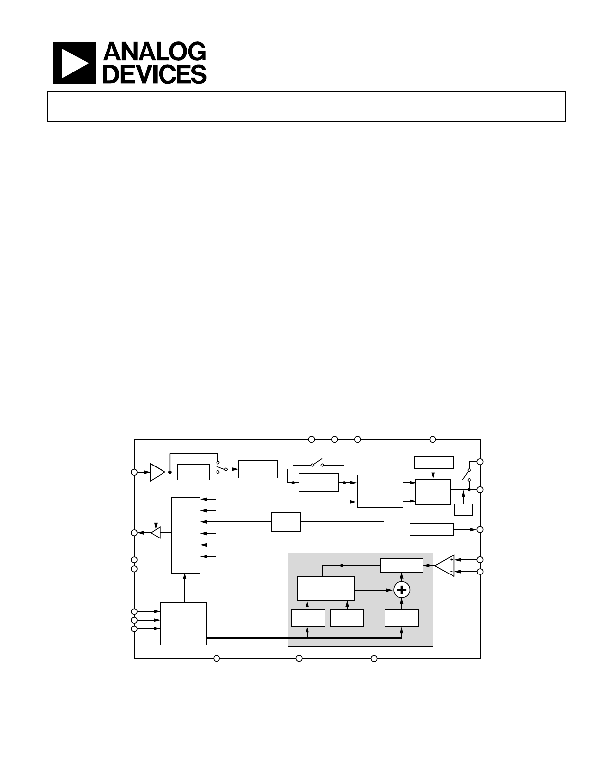
FUNCTIONAL BLOCK DIAGRAM
GENERAL DESCRIPTION
The ADF4158 is a 6.1 GHz, fractional-N frequency synthesizer
with modulation and waveform generation capability. It contains a
25-bit fixed modulus, allowing subhertz resolution at 6.1 GHz.
It consists of a low noise digital phase frequency detector (PFD),
a precision charge pump, and a programmable reference divider.
There is a sigma-delta (Σ-Δ) based fractional interpolator to
allow programmable fractional-N division. The INT and FRAC
registers define an overall N-divider as N = INT + (FRAC/2
The ADF4158 can be used to implement frequency shift keying
(FSK) and phase shift keying (PSK) modulation. There are also
a number of frequency sweep modes available, which generate
various waveforms in the frequency domain, for example,
sawtooth and triangular waveforms. The ADF4158 features
cycle slip reduction circuitry, which leads to faster lock times,
without the need for modifications to the loop filter.
Control of all on-chip registers is via a simple 3-wire interface.
The device operates with a power supply ranging from 2.7 V to
3.3 V and can be powered down when not in use.
25
).
Figure 1.
responsibility is assumed by Analog Devices for its use, nor for any infringements of patents or other
rights of third parties that may result from its use. Specifications subject to change without notice. No
license is granted by implication or otherwise under any patent or patent rights of Analog De vices.
One Technology Way, P.O. Box 9106, Norwood, MA 02062-9106, U.S.A.
Tel: 781.329.4700
www.analog.com

ADF4158 Data Sheet
TABLE OF CONTENTS
Features .............................................................................................. 1
Applications ....................................................................................... 1
General Description ......................................................................... 1
Functional Block Diagram .............................................................. 1
Revision History ............................................................................... 3
Specifications ..................................................................................... 4
Timing Specifications .................................................................. 5
Absolute Maximum Ratings ............................................................ 7
ESD Caution .................................................................................. 7
Pin Configuration and Pin Function Descriptions ...................... 8
Typ i c al Performance Characteristics ............................................. 9
Circuit Description ......................................................................... 11
Reference Input Section ............................................................. 11
RF Input Stage ............................................................................. 11
RF INT Divider ........................................................................... 11
25-Bit Fixed Modulus ................................................................ 11
INT, FRAC, and R Relationship ............................................... 11
R-Counter .................................................................................... 11
Phase Frequency Detector (PFD) and Charge Pump ............ 12
MUXOUT and LOCK Detect ................................................... 12
Input Shift Registers ................................................................... 12
Program Modes .......................................................................... 12
Register Maps .................................................................................. 13
FRAC/INT Register (R0) Map .................................................. 15
LSB FRAC Register (R1) Map ................................................... 16
R-Divider Register (R2) Map .................................................... 17
Function Register (R3) Map ...................................................... 19
Test Register (R4) Map .............................................................. 21
Deviation Register (R5) Map .................................................... 22
Step Register (R6) Map .............................................................. 23
Delay Register (R7) Map ........................................................... 24
Applications Information .............................................................. 25
Initialization Sequence............................................................... 25
RF Synthesizer: A Worked Example ........................................ 25
Reference Doubler and Reference Divider ............................. 25
Cycle Slip Reduction for Faster Lock Times ........................... 25
Modulation .................................................................................. 26
Waveform Generation................................................................ 26
Other Waveforms ....................................................................... 28
Fast-Lock Timer and Register Sequences ............................... 32
Fast Lock: An Example .............................................................. 32
Fast Lock: Loop Filter Topology ............................................... 32
Spur Mechanisms ....................................................................... 33
Low Frequency Applications..................................................... 33
Filter Design—ADIsimPLL ....................................................... 33
PCB Design Guidelines for the Chip Scale Package .............. 33
Application of ADF4158 in FMCW Radar ................................. 34
Outline Dimensions ....................................................................... 35
Ordering Guide ........................................................................... 35
Automotive Products ................................................................. 35
Rev. D | Page 2 of 36

Data Sheet ADF4158
REVISION HISTORY
6/12—Rev. C to Rev. D
Changes to Table 3 and Figure 3 ..................................................... 6
Added Figure 4; Renumbered Sequentially ................................... 6
Added Negative Bleed Current Section ........................................ 21
Changes to Figure 27 ...................................................................... 21
12/11—Rev. B to Rev. C
Changes to Features Section ............................................................ 1
Changes to Figure 6 Caption to Figure 9 Caption ........................ 9
Changes to Figure 11 ...................................................................... 10
Changes to Figure 19 ...................................................................... 12
Changes to Figure 20 ...................................................................... 13
Changed 12-Bit MOD Divider Section to 12-Bit CLK
Divider
1
Section .............................................................................................. 17
Changes to 12-Bit CLK
Divider Section ..................................... 17
1
Changes to Figure 24 ...................................................................... 18
Changes to Delay Clock Select Section and Figure 29 ............... 24
Changes to Timeout Interval Section ........................................... 27
Changes to FMCW Radar Ramp Settings Worked Example
Section .............................................................................................. 28
Changes to Delayed Start, Example Section and Delay Between
Ramps, Example Section ................................................................ 29
Changes to Fast-Lock Timer and Register Sequences Section
and Fast Lock: An Example Section ............................................. 32
Changes to Ordering Guide ........................................................... 35
Added Automotive Products Section ........................................... 35
9/11—Rev. A to Rev. B
Changes to Noise Characteristics Parameter ................................. 3
7/11—Rev. 0 to Rev. A
Changes to Figure 21 ...................................................................... 13
Changes to Figure 25 ...................................................................... 19
Changes to 12-Bit Clock Divider Value Section ......................... 20
Changes to Figure 28 ...................................................................... 22
Changes to FMCW Radar Ramp Settings Worked Example
Section .............................................................................................. 26
Added Ramp Programming Sequence Section, and added
Other Waveforms Heading ............................................................ 27
Changes to Figure 36 ...................................................................... 28
Added Ramp Complete Signal to Muxout Section and changes
to Figure 40 ...................................................................................... 29
Added Figure 42; Renumbered Sequentially ............................... 30
Changes to Figure 45 ...................................................................... 31
Changes to Figure 46 ...................................................................... 33
4/10—Revision 0: Initial Version
Rev. D | Page 3 of 36

ADF4158 Data Sheet
SPECIFICATIONS
AVDD = DVDD = 2.7 V to 3.3 V, VP = AVDD to 5.5 V, AGND = DGND = 0 V, TA = T
otherwise noted.
MIN
to T
, dBm referred to 50 Ω, unless
MAX
Table 1.
1
C Version
Parameter Min Typ Max Unit Test Conditions/Comments
RF CHARACTERISTICS
RF Input Frequency (RFIN) 0.5 6.1 GHz −10 dBm min to 0 dBm max; for lower frequencies, ensure
slew rate (SR) > 400 V/µs
−15 dBm min to 0 dBm max for 2 GHz to 4 GHz RF input
frequency
REFERENCE CHARACTERISTICS
REFIN Input Frequency 10 260 MHz For f < 10 MHz, use a dc-coupled CMOS-compatible
square wave, slew rate > 25 V/µs
16 MHz If an internal reference doubler is enabled
REFIN Input Sensitivity 0.4 AVDD V p-p Biased at AVDD/22
REFIN Input Capacitance 10 pF
REFIN Input Current ±100 µA
PHASE DETECTOR
Phase Detector Frequency3 32 MHz
CHARGE PUMP
ICP Sink/Source Programmable
Hig h Value 5 mA With R
= 5.1 kΩ
SET
Low Value 312.5 µA
Absolute Accuracy 2.5 % With R
R
Range 2.7 10 kΩ
SET
= 5.1 kΩ
SET
ICP Three-State Leakage Current 1 nA Sink and source current
Matching 2 % 0.5 V < VCP < VP – 0.5 V
ICP vs. VCP 2 % 0.5 V < VCP < VP – 0.5 V
ICP vs. Temperature 2 % VCP = VP/2
LOGIC INPUTS
V
, Input High Voltage 1.4 V
INH
V
, Input Low Voltage 0.6 V
INL
I
, Input Current ±1 µA
INH/IINL
CIN, Input Capacitance 10 pF
LOGIC OUTPUTS
VOH, Output High Voltage 1.4 V Open-drain output chosen; 1 kΩ pull-up to 1.8 V
VOH, Output High Voltage VDD − 0.4 V CMOS output chosen
IOH, Output High Current 100 µA
VOL, Output Low Voltage 0.4 V IOL = 500 µA
POWER SUPPLIES
AVDD 2.7 3.3 V
DVDD AVDD
VP AVDD 5.5 V
IDD 23 32 mA
Rev. D | Page 4 of 36
Data Sheet ADF4158
t5
25
ns min
CLK low duration
CLK
DATA
LE
LE
DB31 (MSB) DB30
DB1
(CONTROL BIT C2)
DB2
(CONTROL BIT C3)
DB0 (LSB)
(CONTROL BIT C1)
t
1
t
2
t
3
t
7
t
6
t
4
t
5
08728-026
1
C Version
Parameter Min Typ Max Unit Test Conditions/Comments
NOISE CHARACTERISTICS
Normalized Phase Noise Floor
(PN
)4
SYNTH
Normalized 1/f Noise (PN
)5 −110 dBc/Hz 100 kHz offset; normalized to 1 GHz
1_f
−216 dBc/Hz PLL loop bandwidth = 500 kHz;
measured at 100 kHz offset
Phase Noise Performance6 At VCO output
5805 MHz Output7 −93 dBc/Hz At 5 kHz offset, 32 MHz PFD frequency
1
Operating temperature for C version: −40°C to +125°C.
2
AC coupling ensures AVDD/2 bias.
3
Guaranteed by design. Sample tested to ensure compliance.
4
The synthesizer phase noise floor is estimated by measuring the in-band phase noise at the output of the VCO and subtracting 20 log(N) (where N is the N divider
value) and 10 log(f
5
The PLL phase noise is composed of 1/f (flicker) noise plus the normalized PLL noise floor. The formula for calculating the 1/f noise contribution at an RF frequency, fRF,
and at a frequency offset f is given by PN = PN
6
The phase noise is measured with the EVAL-ADF4158EB1Z and the Agilent E5052A phase noise system.
7
f
= 128 MHz; f
REFIN
). PN
= PN
PFD
SYNTH
= 32 MHz; offset frequency = 5 kHz; RF
PFD
− 10 log(f
TOT
) − 20 log(N).
PFD
+ 10 log(10 kHz/f) + 20 log(fRF/1 GHz). Both the normalized phase noise floor and flicker noise are modeled in ADIsimPLL.
1_f
= 5805 MHz; INT = 181; FRAC = 13631488; loop bandwidth = 100 kHz.
OUT
TIMING SPECIFICATIONS
AVDD = DVDD = SDVDD = 2.7 V to 3.3 V; VP = AVDD to 5.5 V; AGND = DGND = SDGND = 0 V; TA = T
unless otherwise noted.
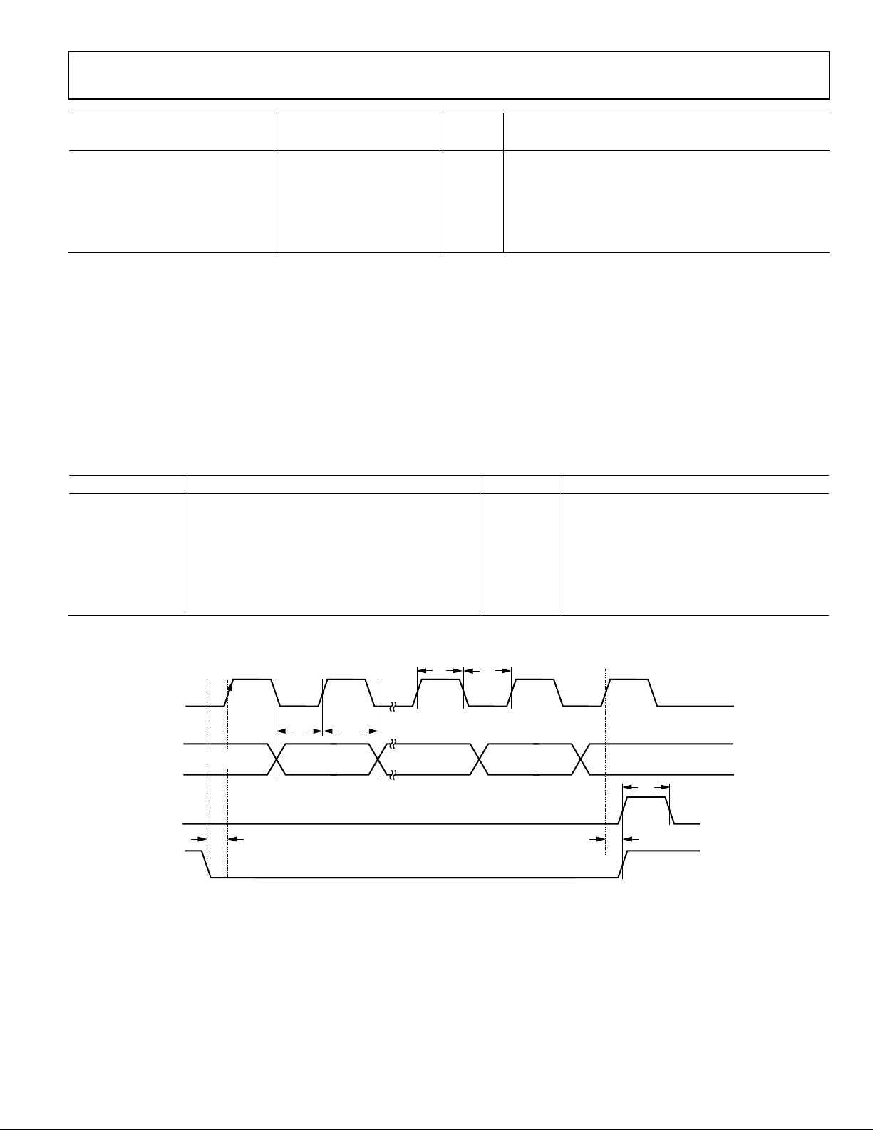
Table 2. Write Timing
Parameter Limit at T
MIN
to T
(C Version) Unit Test Conditions/Comments
MAX
t1 20 ns min LE setup time
t2 10 ns min DATA t o CLK setup time
t3 10 ns min DATA t o CLK hold time
t4 25 ns min CLK high duration
MIN
to T
, dBm referred to 50 Ω,
MAX
t6 10 ns min CLK to LE setup time
t7 20 ns min LE pulse width
Write Timing Diagram
Figure 2. Write Timing Diagram
Rev. D | Page 5 of 36
ADF4158 Data Sheet
CLK
MUXOUT
LE
DB36 DB35 DB1DB2 DB0
08728-226
t
1
t
2
TX
DATA
NOTES
1. LE SHO ULD BE KEPT HIGH DURING READBACK.
t
4
t
5
t
3
100µA
1.5V
I
OL
I
OH
TO OUTPUT
PIN
C
L
10pF
100µA
08728-004
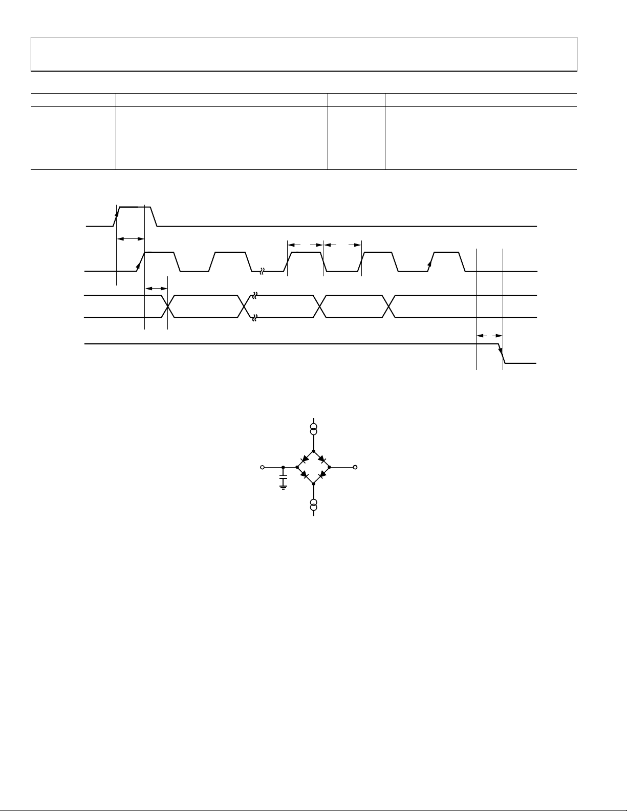
Table 3. Read Timing
Parameter Limit at T
t1 20 ns min TX
t2 20 ns min CLK setup time to DATA (on MUXOUT)
t3 25 ns min CLK high duration
t4 25 ns min CLK low duration
t5 10 ns min CKJ to LE setup time
Read Timing Diagram
MIN
to T
(C Version ) Unit Test Conditions/Comments
MAX
setup time
DATA
Figure 3. Read Timing Diagram
Figure 4. Load Circuit for MUXOUT Timing, C = 10 pF
Rev. D | Page 6 of 36
Data Sheet ADF4158
VDD to GND
−0.3 V to +4 V
Analog I/O Voltage to GND
−0.3 V to VDD + 0.3 V
ABSOLUTE MAXIMUM RATINGS
TA = 25°C, GND = AGND = DGND = SDGND = 0 V,
V
= AVDD = DVDD = SDVDD, unless otherwise noted.
DD
Table 4.
Parameter Rating
VDD to VDD −0.3 V to +0.3 V
VP to GND −0.3 V to +5.8 V
VP to VDD −0.3 V to +5.8 V
Digital I/O Voltage to GND −0.3 V to VDD + 0.3 V
REFIN, RFIN to GND −0.3 V to VDD + 0.3 V
Operating Temperature Range
Industrial (C Version) −40°C to +125°C
Storage Temperature Range −65°C to +125°C
Maximum Junction Temperature 150°C
LFCSP θJA Thermal Impedance
(Paddle Soldered)
Reflow Soldering
Peak Temperature 260°C
Time at Peak Temperature 40 sec
30.4°C/W
Stresses above those listed under Absolute Maximum Ratings
may cause permanent damage to the device. This is a stress
rating only; functional operation of the device at these or any
other conditions above those indicated in the operational
section of this specification is not implied. Exposure to absolute
maximum rating conditions for extended periods may affect
device reliability.
ESD CAUTION
Rev. D | Page 7 of 36

ADF4158 Data Sheet
PIN 1
INDICAT
OR
1CPGND
NOTES
1. THE LFCSP HAS AN EXPOSED PADDLE THAT MUST BE CONNECTE D TO GND.
2AGND
3AGND
4RF
IN
B
5RF
IN
A
6AV
DD
15 DATA
16 LE
17 MUXOUT
18 SDV
DD
14
CLK
13 CE
7AV
DD
8AV
DD
9REF
IN
11SDGND
12TX
DATA
10DGND
21
SW2
22
V
P
23
R
SET
24
CP
20
SW1
19
DV
DD
ADF4158
TOP VIEW
(Not to S cale)
08728-003
1
CPGND
Charge Pump Ground. This is the ground return path for the charge pump.
22
VP
Charge Pump Power Supply. This should be greater than or equal to VDD. In systems where VDD is 3 V, it can be set to
SET
CPmax
R
I
5.25
=
PIN CONFIGURATION AND PIN FUNCTION DESCRIPTIONS
Figure 5. Pin Configuration
Table 5. Pin Function Descriptions
Pin No. Mnemonic Description
2, 3 AGND Analog Ground. This is the ground return path of the prescaler.
4 RFINB Complementary Input to the RF Prescaler. Decouple this point to the ground plane with a small bypass capacitor,
5 RFINA Input to the RF Prescaler. This small-signal input is normally ac-coupled from the VCO.
6, 7, 8 AVDD Positive Power Supply for the RF Section. Place decoupling capacitors to the digital ground plane as close as possible
9 REFIN Reference Input. This is a CMOS input with a nominal threshold of VDD/2 and an equivalent input resistance of 100 kΩ.
10 DGND Digital Ground.
11 SDGND Digital Σ-Δ Modulator Ground. Ground return path for the Σ-Δ modulator.
12 TX
DATA
13 CE Chip Enable. A logic low on this pin powers down the device and puts the charge pump output into three-state mode.
14 CLK Serial Clock Input. This serial clock is used to clock in the serial data to the registers. The data is latched into the shift
15 DATA Serial Data Input. The serial data is loaded MSB first with the three LSBs being the control bits. This input is a high
16 LE Load Enable, CMOS Input. When LE is high, the data stored in the shift registers is loaded into one of the eight latches,
17 MUXOUT Multiplexer Output. This pin allows either the RF lock detect, the scaled RF, or the scaled reference frequency to be
18 SDVDD Power Supply Pin for the Digital Σ-Δ Modulator. This pin should be the same voltage as AVDD. Place decoupling
19 DVDD Positive Power Supply for the Digital Section. Place decoupling capacitors to the digital ground plane as close as
20 , 21 SW1, SW2 Switches for Fast Lock.
typically 100 pF.
to this pin. AV
must have the same voltage as DVDD.
DD
It can be driven from a TTL or CMOS crystal oscillator, or it can be ac-coupled.
Tx Data Pin. Provide data to be transmitted in FSK or PSK mode on this pin.
register on the CLK rising edge. This input is a high impedance CMOS input.
impedance CMOS input.
with the latch being selected using the control bits.
accessed externally.
capacitors to the ground plane as close as possible to this pin.
possible to this pin. DV
must have the same voltage as AVDD.
DD
5.5 V and used to drive a VCO with a tuning range of up to 5.5 V.
23 R
24 CP Charge Pump Output. When enabled, this provides ±ICP to the external loop filter, which in turn drives the external VCO.
25 EPAD Exposed Paddle. The LFCSP has an exposed paddle that must be connected to GND.
Connecting a resistor between this pin and ground sets the maximum charge pump output current. The relationship
SET
between I
where:
I
CPmax
R
SET
CP
= 5 mA.
= 5.1 kΩ.
and R
is
SET
Rev. D | Page 8 of 36
Data Sheet ADF4158
–160
–140
–120
–100
–80
–60
–40
1k 10k 100k 1M 10M
PHASE NOISE (dBc/Hz)
FREQUENCY OFFSET (Hz)
08728-035
5.78
5.79
5.80
5.81
5.82
5.83
5.84
5.85
5.86
–0.025 –0.015 –0.005 0.005 0.015 0.025
FREQUENCY (GHz)
TIME (s)
08728-036
5.75
5.77
5.79
5.81
5.83
5.85
5.87
–0.010 –0.005 0 0.005 0.010
FREQUENCY (GHz)
TIME (s)
08728-037
5.76
5.77
5.78
5.79
5.80
5.81
5.82
5.83
5.84
5.85
5.86
5.87
FREQUENCY (GHz)
TIME (s)
–0.010 –0.005 0 0.005 0.010
08728-039
5.76
5.77
5.78
5.79
5.80
5.81
5.82
5.83
5.84
5.85
5.86
0 0.005 0.010
TIME (s)
FREQUENCY (GHz)
0.015 0.020
NO DELAY
DELAY
08728-040
5.790
5.792
5.794
5.796
5.798
5.800
5.802
5.804
5.806
5.808
5.810
–0.010 0.010–0.005 0.0050
FREQUENCY (GHz)
TIME (s)
08728-041
TYPICAL PERFORMANCE CHARACTERISTICS
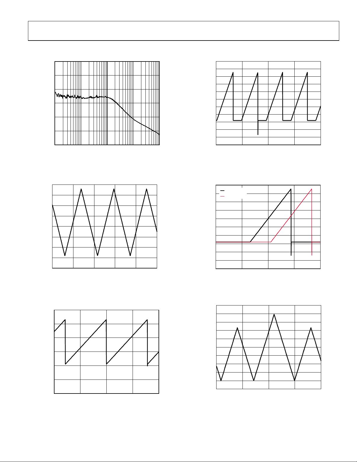
Figure 6. Phase Noise at 5805 MHz, PFD = 32 MHz, Loop Bandwidth = 100 kHz
Figure 7. Triangular Waveform, PFD = 32 MHz, INT = 181, FRAC = 0,
DEV Offset = 4, DEV Word = 20972, Step Word = 200, CLK DIV = 10,
CLK
Divider = 125
1
Figure 9. Delay Between Ramps for Sawtooth Waveform, PFD = 32 MHz,
INT = 181, FRAC = 0, DEV Offset = 4, DEV Word = 20972, Step Word = 200,
CLK DIV = 10, CLK
Divider = 125, DEL Start Word = 1025
1
Figure 10. Delayed Start of Triangular Burst, PFD = 32 MHz, INT = 181,
FRAC = 0, DEV Offset = 4, DEV Word = 20972, Step Word = 200,
CLK DIV = 10, CLK
Divider = 125, DEL Start Word = 1000
1
Figure 8. Sawtooth Waveform, PFD = 32 MHz, INT = 181, FRAC = 0,
DEV Offset = 4, DEV Word = 20972, Step Word = 200, CLK DIV = 10,
CLK
Divider = 125
1
Figure 11. Dual Ramp Rate Waveform, PFD = 32 MHz, INT = 181, FRAC = 0,
Ramp 1: DEV Offset = 3, DEV Word = 16777, Step Word = 100,
Ramp 2: DEV Offset = 3, DEV Word = 20792, Step Word = 80
Rev. D | Page 9 of 36
ADF4158 Data Sheet
5.7995
5.7996
5.7997
5.7998
5.7999
5.8000
5.8001
5.8002
5.8003
5.8004
FREQUENCY (GHz)
–0.010 0.010–0.005 0.0050
TIME (s)
08728-042
5.79975
5.79980
5.79985
5.79990
5.79995
5.80005
5.80000
5.80010
0 0.1 0.2 0.3 0.4 0.5 0.6 0.7 0.8 0.9 1.0
FREQUENCY (GHz)
TIME (ms)
08728-044
–30
–25
–20
–15
–10
–5
0
0.185 1.185 2.185 3.185 4.185 5.185 6.185 7.185
POWER (dBm)
FREQUENCY (GHz)
08728-128
–8
–6
–4
–2
I
CP
(mA)
0
2
4
6
0 1 2 3
V
CP
(V)
4 5 6
08728-046
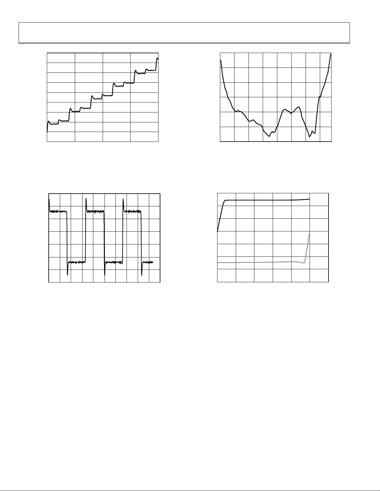
Figure 12. FSK Superimposed on Rising Edge of Triangular Waveform;
Ramp Settings: PFD = 32 MHz, INT = 181, FRAC = 0, DEV Offset = 4, DEV
Word = 20972, Step Word = 200, CLK DIV = 10, CLK
Divider = 125;
1
FSK Settings: DEV Offset = 3, DEV Word = 4194
Figure 13. FSK; Settings: Frequency Deviation = 100 kHz, Data Rate = 3 kHz
Figure 14. RF
Sensitivity-Average Over Temperature and V
IN
DD
Figure 15. Charge Pump Output Characteristics
Rev. D | Page 10 of 36
Data Sheet ADF4158
BUFFER
TO R-COUNTER
REF
IN
100kΩ
NC
SW2
SW3
NO
NC
SW1
POWER-DOWN
CONTROL
08728-027
BIAS
GENERATOR
1.6V
AGND
AV
DD
2kΩ 2kΩ
RF
IN
B
RF
IN
A
08728-015
THIRD-ORDER
FRACTIONAL
INTERPOLATOR
FRAC
VALUE
MOD
REG
INT
REG
RF N-DIVI DE R
N = INT + FRAC/MOD
FROM RF
INPUT STAGE
TO PFD
N-COUNTER
08728-016
CIRCUIT DESCRIPTION
REFERENCE INPUT SECTION
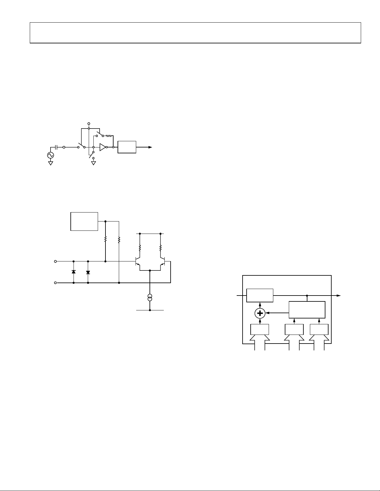
The reference input stage is shown in Figure 16. SW1 and SW2
are normally closed switches. SW3 is normally open. When
power-down is initiated, SW3 is closed and SW1 and SW2 are
opened. This ensures that there is no loading of the REF
IN
pin
on power-down.
Figure 16. Reference Input Stage
RF INPUT STAGE
The RF input stage is shown in Figure 17. It is followed by a
2-stage limiting amplifier to generate the current-mode logic
(CML) clock levels needed for the prescaler.
25-BIT FIXED MODULUS
The ADF4158 has a 25-bit fixed modulus. This allows output
frequencies to be spaced with a resolution of
f
= f
RES
where f
/225 (1)
PFD
is the frequency of the phase frequency detector
PFD
(PFD). For example, with a PFD frequency of 10 MHz,
frequency steps of 0.298 Hz are possible.
INT, FRAC, AND R RELATIONSHIP
The INT and FRAC values, in conjunction with the R-counter,
make it possible to generate output frequencies that are spaced
by fractions of the phase frequency detector (PFD). The RF VCO
frequency (RF
RF
OUT
where:
RF
is the output frequency of external voltage controlled
OUT
oscillator (VCO).
INT is the preset divide ratio of binary 12-bit counter (23 to 4095).
FRAC is the numerator of the fractional division (0 to 2
f
= REFIN × [(1 + D)/(R × (1 + T))] (3)
PFD
where:
REF
is the reference input frequency.
IN
D is the REF
T is the REF
R is the preset divide ratio of the binary, 5-bit, programmable
reference counter (1 to 32).
) equation is
OUT
= f
× (INT + (FRAC/225)) (2)
PFD
doubler bit (0 or 1).
IN
divide-by-2 bit (0 or 1).
IN
25
− 1).
Figure 17. RF Input Stage
RF INT DIVIDER
The RF INT CMOS counter allows a division ratio in the PLL
feedback counter. Division ratios from 23 to 4095 are allowed.
Figure 18. RF N-Divider
R-COUNTER
The 5-bit R-counter allows the input reference frequency (REFIN)
to be divided down to produce the reference clock to the PFD.
Division ratios from 1 to 32 are allowed.
Rev. D | Page 11 of 36
 Loading...