

A
www.BDTIC.com/ADI
Fractional-N Frequency Synthesizer
FEATURES
RF bandwidth to 4 GHz
2.7 V to 3.3 V power supply
Separate V
Programmable dual-modulus prescaler 4/5, 8/9
Programmable charge pump currents
3-wire serial interface
Digital lock detect
Power-down mode
Pin compatible with the ADF4110/ADF4111/
ADF4112/ADF4113, ADF4106, ADF4153
Programmable modulus on fractional-N synthesizer
Trade-off noise vs. spurious performance
Fast-lock mode with built-in timer
Loop filter design possible with ADIsimPLL™
APPLICATIONS
Base stations for mobile radio (WiMAX, PHS, GSM, PCS, DCS,
CDMA, PMR, W-CDMA, supercell 3G)
Wireless handsets (PMR, GSM, PCS, DCS, CDMA, WCDMA)
CATV equipment
Wireless LANs
Communications test equipment
allows extended tuning voltage
P
ADF4154
GENERAL DESCRIPTION
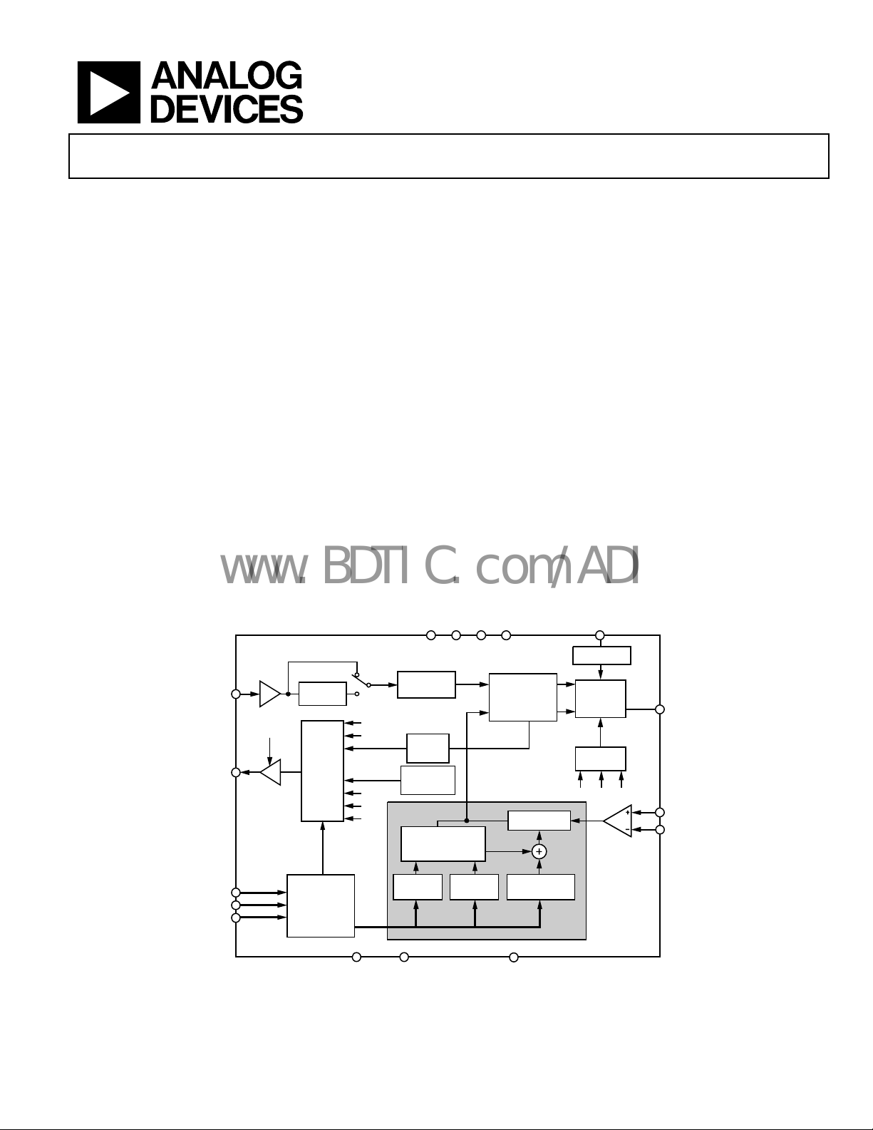
The ADF4154 is a fractional-N frequency synthesizer that
implements local oscillators in the up conversion and down
conversion sections of wireless receivers and transmitters. It
consists of a low noise digital phase frequency detector (PFD),
a precision charge pump, and a programmable reference divider.
There is a Σ-Δ based fractional interpolator to allow programmable
fractional-N division. The INT, FRAC, and MOD registers define
an overall N-divider (N = (INT + (FRAC/MOD))). In addition,
the 4-bit reference counter (R-counter) allows selectable REF
frequencies at the PFD input. A complete phase-locked loop (PLL)
can be implemented if the synthesizer is used with an external
loop filter and a voltage-controlled oscillator (VCO).
A key feature of the ADF4154 is the fast-lock mode with a builtin t
imer. The user can program a predetermined countdown
time value so that the PLL remains in wide bandwidth mode,
instead of the user having to control this time externally.
Control of all on-chip registers is via a simple 3-wire interface.
The de
vice operates with a power supply ranging from 2.7 V to
3.3 V and can be powered down when not in use.
IN
REF
MUXOUT
CLOCK
DATA
IN
LE
ADF4154
HIGH Z
FUNCTIONAL BLOCK DIAGRAM
V
DV
DD
DDVP
4-BIT
×2
DOUBLER
OUTPUT
MUX
24-BIT
DATA
REGISTER
AGND
R COUNTER
V
DD
DGND
V
DD
R
DIV
N
DIV
LOCK
DETECT
FAST-LOCK
SWITCH
THIRD ORDER
FRACTIONAL
INTERPOLATOR
REG
MODULUS
Figure 1.
FRACTION
DGND CPGND
REG
SDV
DD
+
PHASE
FREQUENCY
DETECT OR
–
N COUNTER
INTEGER REG
R
SET
REFERENCE
CHARGE
PUMP
CURRENT
SETTING
RFCP3 RFCP2 RFCP1
CP
RFINA
RF
IN
B
04833-001
Rev. A
Information furnished by Analog Devices is believed to be accurate and reliable. However, no
responsibility is assumed by Anal og Devices for its use, nor for any infringements of patents or ot her
rights of third parties that may result from its use. Specifications subject to change without notice. No
license is granted by implication or otherwise under any patent or patent rights of Analog Devices.
Trademarks and registered trademarks are the property of their respective owners.
One Technology Way, P.O. Box 9106, Norwood, MA 02062-9106, U.S.A.
Tel: 781.329.4700 www.analog.com
Fax: 781.461.3113 ©2006 Analog Devices, Inc. All rights reserved.

ADF4154
www.BDTIC.com/ADI
TABLE OF CONTENTS
Features.............................................................................................. 1
Applications....................................................................................... 1
General Description ......................................................................... 1
Functional Block Diagram .............................................................. 1
Revision History ............................................................................... 2
Specifications..................................................................................... 3
Timing Characteristics ................................................................ 4
Absolute Maximum Ratings............................................................ 5
ESD Caution.................................................................................. 5
Pin Configuration and Pin Function Descriptions...................... 6
Typical Performance Characteristics ............................................. 7
Circuit Description........................................................................... 9
Reference Input Section............................................................... 9
RF Input Stage............................................................................... 9
RF INT Divider............................................................................. 9
INT, FRAC, MOD, and R Relationship ..................................... 9
R-Counter...................................................................................... 9
Phase Frequency Detector (PFD) and Charge Pump.............. 9
MUXOUT and Lock Detect...................................................... 10
Input Shift Registers................................................................... 10
Program Modes .......................................................................... 10
Registers........................................................................................... 11
Register Definitions ................................................................... 16
R-Divider Register, R1 ............................................................... 16
Control Register, R2................................................................... 16
Noise and Spur Register, R3...................................................... 17
Reserved Bits............................................................................... 17
Initialization Sequence .............................................................. 18
RF Synthesizer: A Worked Example........................................ 18
Modulus....................................................................................... 18
Reference Doubler and Reference Divider ............................. 18
12-Bit Programmable Modulus................................................ 18
Spurious Optimization and Fast lock ...................................... 18
Fast-Lock Timer and Register Sequences ............................... 19
Fast Lock: An Example.............................................................. 19
Fast Lock: Loop Filter Topology............................................... 19
Spur Mechanisms....................................................................... 19
Spur Consistency........................................................................ 20
Filter Design—ADIsimPLL....................................................... 20
Interfacing ................................................................................... 20
PCB Design Guidelines for Chip Scale Package .................... 21
Outline Dimensions....................................................................... 22
Ordering Guide .......................................................................... 22
REVISION HISTORY
12/06—Rev. 0 to Rev. A
Changes to Features.......................................................................... 1
Changes to Applications .................................................................. 1
Changes to Functional Block Diagram.......................................... 1
Changes to Specifications................................................................ 3
Changes to Absolute Maximum Ratings....................................... 5
Changes to Typical Performance Characteristics Conditions.... 7
Replaced Figure 5 through Figure 7............................................... 7
Changes to Figure 13........................................................................ 8
Changes to R-Divider Register Map ............................................ 13
Changes to Control Register Map ................................................14
Change to REF
Added Initialization Sequence Section........................................ 18
Doubler Section................................................ 18
IN
Rev. A | Page 2 of 24
Change to 12-Bit Programmable Modulus Section................... 18
Changes to Fast-Lock Timer and Register Sequences Section........19
Changes to Fast Lock: Loop Filter Topology Section ................ 19
Deleted Spurious Signal Section................................................... 18
Added Spur Mechanisms Section ................................................ 19
Added Spur Consistency Section ................................................. 20
Change to Filter Design—ADIsimPLL Section.......................... 20
Change to Interfacing Section ...................................................... 20
Updated Outline Dimensions....................................................... 22
Changes to Ordering Guide.......................................................... 22
5/04—Revision 0: Initial Version

ADF4154
www.BDTIC.com/ADI
SPECIFICATIONS
AVDD = DVDD = SDVDD = 2.7 V to 3.3 V; VP = AVDD to 5.5 V; AGND = DGND = 0 V; TA = T
referred to 50 Ω. The operating temperature for the B version is −40°C to +80°C.
Table 1.
Parameter B Version Unit Test Conditions/Comments
RF CHARACTERISTICS (3 V)
RF Input Frequency (RFIN)
1
0.5/4.0 GHz min/max −8 dBm/0 dBm min/max. For lower frequencies, ensure slew rate > 400 V/μs.
See Figure 15 for the input circuit.
1.0/4.0 GHz min/max −10 dBm/0 dBm min/max.
REFERENCE CHARACTERISTICS See Figure 14 for input circuit.
REFIN Input Frequency
REFIN Input Sensitivity 0.7/AVDD V p-p min/max Biased at AVDD/2.
1
10/250 MHz min/max
For f < 10 MHz, use a dc-coupled, CMOS-compatible square wave,
slew ra
te > 25 V/μs.
2
REFIN Input Capacitance 10 pF max
REFIN Input Current ±100 μA max
PHASE DETECTOR
Phase Detector Frequency
3
32 MHz max
CHARGE PUMP
ICP Sink/Source Programmable. See Table 5.
High Value 5 mA typ With R
= 5.1 kΩ.
SET
Low Value 312.5 μA typ
Absolute Accuracy 2.5 % typ With R
R
Range 2.7/10 kΩ min/max
SET
= 5.1 kΩ.
SET
ICP Three-State Leakage Current 1 nA typ Sink and source current.
Matching 2 % typ 0.5 V < VCP < VP − 0.5 V.
ICP vs. VCP 2 % typ 0.5 V < VCP < VP − 0.5 V.
ICP vs. Temperature 2 % typ VCP = VP/2.
LOGIC INPUTS
V
, Input High Voltage 1.4 V min
INH
V
, Input Low Voltage 0.6 V max
INL
I
, Input Current ±1 μA max
INH/IINL
CIN, Input Capacitance 10 pF max
LOGIC OUTPUTS
VOH, Output High Voltage 1.4 V min Open-drain 1 kΩ pull-up to 1.8 V.
VOL, Output Low Voltage 0.4 V max IOL = 500 μA.
POWER SUPPLIES
AVDD 2.7/3.3 V min/V max
DVDD, SDVDD AVDD
VP AVDD/5.5 V min/V max
IDD 24 mA max 20 mA typical.
Low Power Sleep Mode 1 μA typ
NOISE CHARACTERISTICS
Phase Noise Figure of Merit
Phase Noise Performance
1750 MHz Output
1
Use a square wave for frequencies below f
2
AC coupling ensures AVDD/2 bias. See Figure 14 for a typical circuit.
3
Guaranteed by design. Sample tested to ensure compliance.
4
This value can be used to calculate phase noise for any application. Use the formula –213 + 10 log(f
seen at the VCO output. The value given is the lowest noise mode.
5
The phase noise is measured with the EVAL-ADF4154EB1 and the HP8562E spectrum analyzer.
6
f
= 26 MHz, f
REFIN
= 26 MHz, offset frequency = 1 kHz, RF
PFD
4
5
6
−213 dBc/Hz typ
@ VCO output.
−102 dBc/Hz typ @ 1 kHz offset, 26 MHz PFD frequency.
.
MIN
) + 20 log N to calculate the in-band phase noise performance, as
PFD
= 1750 MHz, loop B/W = 20 kHz, lowest noise mode.
OUT
MIN
to T
, unless otherwise noted; dBm
MAX
Rev. A | Page 3 of 24

ADF4154
www.BDTIC.com/ADI
TIMING CHARACTERISTICS
AVDD = DVDD = SDVDD = 2.7 V to 3.3 V; VP = AVDD to 5.5 V; AGND = DGND = 0 V; TA = T
referred to 50 Ω.
MIN
to T
, unless otherwise noted; dBm
MAX
Table 2.
Parameter
1
Limit at T
MIN
to T
(B Version) Unit Test Conditions/Comments
MAX
t1 20 ns min LE setup time
t2 10 ns min DATA to CLOCK setup time
t3 10 ns min DATA to CLOCK hold time
t4 25 ns min CLOCK high duration
t5 25 ns min CLOCK low duration
t6 10 ns min CLOCK to LE setup time
t7 20 ns min LE pulse width
1
Guaranteed by design, but not production tested.
CLOCK
DATA
LE
LE
t
2
DB23 (MSB) DB22 DB2
t
1
t
3
Figure 2. Timing Diagram
t
4
t
5
DB1
(CONTROL BIT C2)
DB0 (LSB)
(CONTROL BIT C1)
t
7
t
6
04833-026
Rev. A | Page 4 of 24
ADF4154
www.BDTIC.com/ADI
ABSOLUTE MAXIMUM RATINGS
TA = 25°C, unless otherwise noted.
Table 3.
GND
= D
GND
3
= 0 V.
Rating
30.4°C/W
Parameter1, 2,
VDD to GND −0.3 V to +4 V
VDD to VDD −0.3 V to +0.3 V
VP to GND −0.3 V to +5.8 V
VP to VDD −0.3 V to +5.8 V
Digital I/O Voltage to GND −0.3 V to VDD + 0.3 V
Analog I/O Voltage to GND −0.3 V to VDD + 0.3 V
REFIN, RFIN to GND −0.3 V to VDD + 0.3 V
Operating Temperature Range
Industrial (B Version) −40°C to +85°C
Storage Temperature Range −65°C to +150°C
Maximum Junction Temperature 150°C
TSSOP θJA Thermal Impedance 112°C/W
LFCSP θJA Thermal Impedance
(Paddle Soldered)
Reflow Soldering
Peak Temperature 260°C
Time at Peak Temperature 40 sec
1
This device is a high performance RF-integrated circuit with an ESD rating of
<2 kV, and it is ESD sensitive. Proper precautions should be taken when
handling and assembling the device.
2
GND = A
3
VDD = AVDD = DVDD = SDVDD.
Stresses above those listed under Absolute Maximum Ratings
may cause permanent damage to the device. This is a stress
rating only; functional operation of the device at these or any
other conditions above those listed in the operational sections
of this specification is not implied. Exposure to absolute
maximum rating conditions for extended periods may affect
device reliability.
ESD CAUTION
Rev. A | Page 5 of 24
ADF4154
www.BDTIC.com/ADI
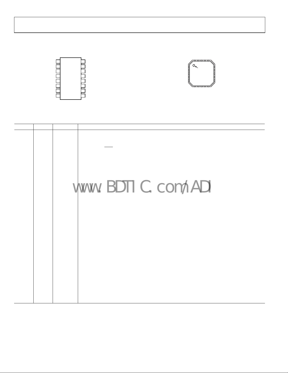
PIN CONFIGURATION AND PIN FUNCTION DESCRIPTIONS
DD
SET
CP
R
VPDVDDDV
20
191817
R
SET
CP
CPGND
AGND
RFINB
RFINA
AV
REF
DD
IN
1
2
3
ADF4154
4
TOP VIEW
5
(Not to Scale)
6
7
8
16
15
14
13
12
11
10
9
V
P
DV
DD
MUXOUT
LE
DATA
CLK
SDV
DD
DGND
04833-002
Figure 3. TSSOP Pin Configuration
Table 4. Pin Function Descriptions
TSSOP LFCSP Mnemonic Description
1 19 R
2 20 CP
SET
Set Resistor. Connecting a resistor between this pin and ground sets the maximum charge pump
output curr
where R
ent. The relationship between I
I
=
CPmax
R
= 5.1 kΩ and I
SET
Charge Pump Output. When enabled, this pin provides ±I
drives the external VCO.
3 1 CPGND
4 2, 3 AGND
5 4 RF
B
IN
Charge Pump Ground. This is the ground return path for the charge pump.
Analog Ground. This is the ground return path of the prescaler.
Complementary Input to the RF Prescaler. This point should be decoupled to the ground plane with a
small bypass capacitor, typically 100 pF (see Figure 15).
6 5 RF
7 6, 7 AV
A Input to the RF Prescaler. This small-signal input is normally ac-coupled from the VCO.
IN
DD
Positive Power Supply for the RF Section. Decoupling capacitors to the digital ground plane should be placed
as close as possible to this pin. AV
8 8 REF
IN
Reference Input. This CMOS input has a nominal threshold of V
100 kΩ (see Figure 14). This input can be driven from a TTL or CMOS crystal oscillator, or it can be ac-coupled.
9 9, 10 DGND Digital Ground.
10 11 SDV
11 12 CLK
DD
Σ-∆ Power. Decoupling capacitors to the digital ground plane should be placed as close as possible to
this pin. SDV
DD
Serial Clock Input. This serial clock is used to clock in the serial data to the registers. The data is latched
into the shift register on the CLK rising edge. This input is a high impedance CMOS input.
12 13 DATA
Serial Data Input. The serial data is loaded MSB first with the two LSBs as the control bits. This input is a
high impedance CMOS input.
13 14 LE
Load Enable, CMOS Input. When LE is high, the data stored in the shift registers is loaded into one of the
four latches, which is selected by the user via the control bits.
14 15 MUXOUT
Multiplexer Output. This pin allows either the RF lock detect, the scaled RF, or the scaled reference
frequency to be accessed externally.
15 16, 17 DV
DD
Positive Power Supply for the Digital Section. Decoupling capacitors to the digital ground plane should
be placed as close as possible to this pin. DV
16 18 V
voltage as AV
P
Charge Pump Power Supply. This should be greater than or equal to V
DD
can be set to 5.5 V and used to drive a VCO with a tuning range of up to 5.5 V.
1
CPGND
2
AGND
AGND
RF
IN
RFINA
B
3
4
(Not to S cale)
5
ADF4154
TOP VIEW
Figure 4. LFCSP Pin Configuration
SET
and R
CP
5.25
= 5 mA.
CPmax
has a value of 3 V ± 10%. AVDD must have the same voltage as DVDD.
DD
SET
is
to the external loop filter, which in turn
CP
/2 and an equivalent input resistance of
DD
has a value of 3 V ± 10%. SDVDD must have the same voltage as DVDD.
has a value of 3 V ± 10%. DVDD must have the same
DD
.
16
15
PIN 1
INDICATOR
678
DD
AVDDAV
IN
REF
DD
MUXOUT
LE
14
DATA
13
CLK
12
SDV
11
DD
9
10
DGND
DGND
. In systems where VDD is 3 V, it
04833-003
Rev. A | Page 6 of 24

ADF4154
–
–
–
–
www.BDTIC.com/ADI
TYPICAL PERFORMANCE CHARACTERISTICS
Loop bandwidth = 20 kHz; reference = 250 MHz; VCO = Vari-L Company, Inc., VCO190-1750T; evaluation board = EVAL-ADF4154EB1;
measurements taken with the Agilent E5500 phase noise measurement system.
30
20kHz LOOP BW, LO W NOISE MODE
–40
RF = 1.7202MHz, PFD = 25MHz , N = 68,
–50
FRAC = 101, MO D = 125, I
INTEGRATED PHASE ERRO R = 0.23° rms
–60
SIRENZA 1750T VCO
–70
–80
–90
–100
–110
–120
–130
PHASE NOISE (dBc/Hz)
–140
–150
–160
–170
1k 10k 1M 10M 100M
= 625µA, DSB
CP
100k
FREQUENCY (Hz)
Figure 5. Single-Sideband Phase Noise Plot (Lowest Noise Mode)
04833-004
130
–140
–150
PHASE NOISE (dBc/Hz)
–160
–170
100 1000 10000 100000
PHASE DETEC TOR FREQUE NCY (kHz)
Figure 8. PFD Noise Floor vs. PFD Frequency (Lowest Noise Mode)
04833-010
30
20kHz LOOP BW, LO W NOISE AND SPUR MODE
–40
RF = 1.7202MHz, PFD = 25MHz, N = 68,
–50
FRAC = 101, MOD = 125, I
INTEGRATED PHASE ERROR = 0.33° rms
–60
SIRENZA 1750T VCO
–70
–80
–90
–100
–110
–120
–130
PHASE NOISE (dBc/Hz)
–140
–150
–160
–170
1k 10k 1M 10M 100M
= 625µA, DSB
CP
100k
FREQUENCY (Hz)
Figure 6. Single-Sideband Phase Noise Plot
(Low N
oise Mode and Spur Mode)
30
20kHz LOOP BW, LO W SPUR MODE
–40
RF = 1.7202MHz, PFD = 25MHz, N = 68,
–50
FRAC = 101, MOD = 125, I
INTEGRATED PHASE ERROR = 0.36° rms
–60
SIRENZA 1750T VCO
–70
–80
–90
–100
–110
–120
–130
PHASE NOISE (dBc/Hz)
–140
–150
–160
–170
1k 10k 1M 10M 100M
= 625µA, DSB
CP
100k
FREQUENCY (Hz)
Figure 7. Single-Sideband Phase Noise Plot (Lowest Spur Mode)
5
0
–5
–10
–15
–20
AMPLITUDE (dBm)
–25
–30
04833-005
–35
0 0.5 1.0 1.5 4.03.53.02.52.0 4.5
FREQUENCY ( GHz)
P = 4/5
P = 8/9
04833-011
Figure 9. RF Input Sensitivity
6
5
4
3
2
1
0
(mA)
–1
CP
I
–2
–3
–4
–5
04833-006
–6
012345
VCP(V)
04833-012
Figure 10. Charge Pump Output Characteristics
Rev. A | Page 7 of 24

ADF4154
–
–
C
www.BDTIC.com/ADI
Y (GHz)
FREQUEN
1.700
1.696
1.692
1.688
1.684
1.680
1.676
1.672
1.668
1.664
1.660
1.656
1.652
1.648
1.644
1.640
LOCK TIME IN FAST-LOCK MODE
(FAST COUNT ER = 150)
LOCK TIME IN NORMAL MO DE
LOW SPUR MODE:
1649.7MHz TO 1686.8MHz
FINAL LO OP BANDWIDTH = 60kHz
TIME (µs)
Figure 13. Frequency vs. Lock Time
1100 102030405060708090100
04833-028
80
–85
–90
–95
–100
PHASE NOISE ( dBc/Hz)
–105
–110
03
R
VAL UE (k Ω)
SET
Figure 11. Phase Noise vs. R
SET
530252015105
04833-013
PHASE NOISE (dBc/Hz)
90
–92
–94
–96
–98
–100
–102
–104
–60 100–40
–20 0 20 40 60
TEMPERATURE (° C)
80
04833-014
Figure 12. Phase Noise vs. Temperature
Rev. A | Page 8 of 24
 Loading...