Analog Devices ADF4001BRU, ADF4001BCP Datasheet

a
200 MHz Clock Generator PLL
ADF4001
FEATURES
200 MHz Bandwidth
2.7 V to 5.5 V Power Supply
Separate Charge Pump Supply (V
) Allows Extended
P
Tuning Voltage in 5 V Systems
Programmable Charge Pump Currents
3-Wire Serial Interface
Hardware and Software Power-Down Mode
Analog and Digital Lock Detect
Hardware-Compatible to the ADF4110/ADF4111/
ADF4112/ADF4113
Typical Operating Current 4.5 mA
Ultralow Phase Noise
16-Lead TSSOP
20-Lead Chip Scale Package
APPLICATIONS
Clock Generation
Low Frequency PLLs
Low Jitter Clock Source
Clock Smoothing
Frequency Translation
SONET, ATM, ADM, DSLAM, SDM
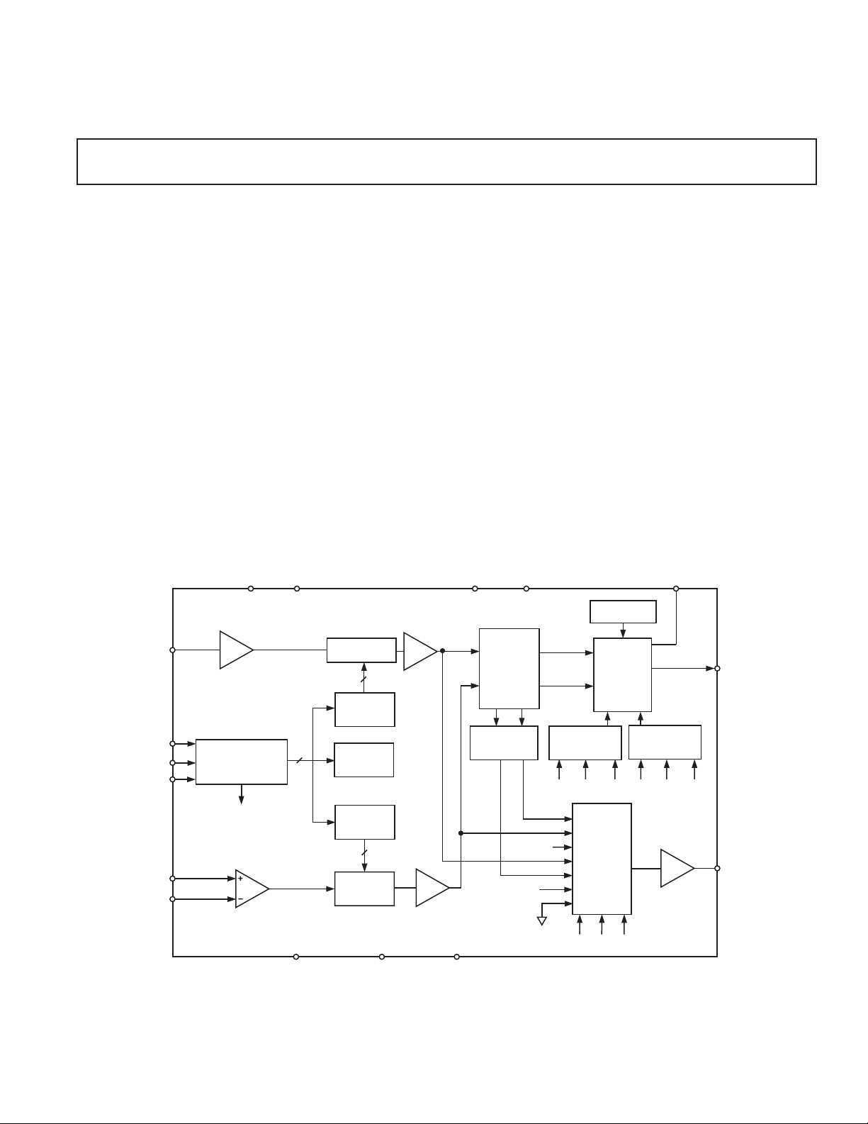
FUNCTIONAL BLOCK DIAGRAM
AV
ADF4001
DV
DD
DD
GENERAL DESCRIPTION
The ADF4001 clock generator can be used to implement clock
sources for PLLs that require very low noise, stable reference signals. It consists of a low-noise digital PFD (Phase
Frequency Detector), a precision charge pump, a programmable
reference divider, and a programmable 13-bit N counter. In
addition, the 14-bit reference counter (R Counter) allows
selectable REFIN frequencies at the PFD input. A complete
PLL (Phase-Locked Loop) can be implemented if the synthesizer
is used with an external loop filter and VCO (Voltage Controlled
Oscillator) or VCXO (Voltage Controlled Crystal Oscillator).
The N min value of 1 allows flexibility in clock generation.
V
CPGND
P
REFERENCE
R
SET
REF
CLK
DATA
RFINA
RF
IN
IN
24-BIT
INPUT REGISTER
LE
SD
OUT
B
22
CE AGND DGND
14-BIT
R COUNTER
14
R COUNTER
LATCH
FUNCTION
LATCH
N COUNTER
LATCH
13
13-BIT
N COUNTER
REV. 0
Information furnished by Analog Devices is believed to be accurate and
reliable. However, no responsibility is assumed by Analog Devices for its
use, nor for any infringements of patents or other rights of third parties that
may result from its use. No license is granted by implication or otherwise
under any patent or patent rights of Analog Devices.
PHASE
FREQUENCY
DETECTOR
LOCK DETECT
CPI3
AV
DD
SD
OUT
One Technology Way, P.O. Box 9106, Norwood, MA 02062-9106, U.S.A.
Tel: 781/329-4700 www.analog.com
Fax: 781/326-8703 © Analog Devices, Inc., 2001
CURRENT
SETTING 1
CPI2
MUX
M3
CHARGE
PUMP
CPI1
M2
M1
CURRENT
SETTING 2
CPI6
CPI5
HIGH Z
CP
CPI4
MUXOUT

ADF4001–SPECIFICATIONS
CPGND = 0 V; R
Parameter B Version Unit Test Conditions/Comments
RF CHARACTERISTICS (3 V) See Figure 3 for Input Circuit
RF Input Frequency 5/165 MHz min/max
RF Input Sensitivity –10/0 dBm min/max
RF CHARACTERISTICS (5 V)
RF Input Frequency 10/200 MHz min/max –5/0 dBm min/max
REFIN CHARACTERISTICS See Figure 2 for Input Circuit
REFIN Input Frequency 5/100 MHz min/max For f < 5 MHz, Use DC-Coupled Square Wave
REFIN Input Sensitivity
REFIN Input Capacitance 10 pF max
REFIN Input Current ± 100 µA max
PHASE DETECTOR
Phase Detector Frequency
CHARGE PUMP
Sink/Source Programmable: See Table V
I
CP
High Value 5 mA typ With R
Low Value 625 µA typ
Absolute Accuracy 2.5 % typ With R
R
SET
I
Three-State Leakage Current 1 nA typ
CP
Sink and Source Current Matching 2 % typ 0.5 V ≤ V
I
vs. V
CP
ICP vs. Temperature 2 % typ VCP = VP/2
LOGIC INPUTS
V
, Input High Voltage 0.8 × DV
INH
, Input Low Voltage 0.2 × DV
V
INL
I
INH/IINL
CIN, Input Capacitance 10 pF max
LOGIC OUTPUTS
VOH, Output High Voltage DVDD – 0.4 V min IOH = 500 µA
VOL, Output Low Voltage 0.4 V max IOL = 500 µA
POWER SUPPLIES
AV
DD
DV
DD
V
P
4
I
(AIDD + DIDD)
DD
ADF4001 5.5 mA max 4.5 mA typical
I
P
Low Power Sleep Mode 1 µA typ
NOISE CHARACTERISTICS
ADF4001 Phase Noise Floor
Phase Noise Performance
200 MHz Output
Spurious Signals
200 MHz Output
NOTES
1
Operating temperature range is as follows: B Version: –40°C to +85°C.
2
AVDD = DVDD = 3 V; for AVDD = DVDD = 5 V, use CMOS-compatible levels.
3
Guaranteed by design. Sample tested to ensure compliance.
4
TA = 25°C; AVDD = DVDD = 3 V; RFIN = 100 MHz.
5
The synthesizer phase noise floor is estimated by measuring the in-band phase noise at the output of the VCO and subtracting 20 logN (where N is the N divider value).
6
The phase noise is measured with the EVAL-ADF4001EB1 Evaluation Board and the HP8562E Spectrum Analyzer.
7
f
= 10 MHz; f
REFIN
Specifications subject to change without notice.
= 4.7 k; TA = T
SET
MIN
to T
unless otherwise noted; dBm referred to 50 )
MAX
20/200 MHz min/max –10/0 dBm min/max
2
3
–5 dBm min AC-Coupled. When DC-Coupled:
55 MHz max
Range 2.7/10 kΩ typ See Table V
CP
1.5 % typ 0.5 V ≤ VCP ≤ VP – 0.5
, Input Current ± 1 µA max
2.7/5.5 V min/V max
AV
DD
AVDD/6.0 V min/V max AVDD ≤ VP ≤ 6.0 V
0.4 mA max TA = 25°C
5
6
7
7
= 200 kHz; Offset frequency = 1 kHz; fRF = 200 MHz; N = 1000; Loop B/W = 20 kHz.
PFD
–161 dBc/Hz typ @ 200 kHz PFD Frequency
–153 dBc/Hz typ @ 1 MHz PFD Frequency
–99 dBc/Hz typ @ 1 kHz Offset and 200 kHz PFD Frequency
–90/–95 dBc typ/dBc typ @ 200 kHz/400 kHz and 200 kHz PFD Frequency
DD
DD
(AV
= DVDD = 3 V 10%, 5 V 10%; AVDD ≤ VP ≤ 6.0 V ; AGND = DGND =
DD
(0 to V
0 to V
)
DD
max (CMOS-Compatible)
DD
= 4.7 kΩ
SET
= 4.7 kΩ
SET
≤ VP – 0.5
CP
V min
V max
@ VCXO Output
1
–2–
REV. 0

ADF4001
WARNING!
ESD SENSITIVE DEVICE
(AV
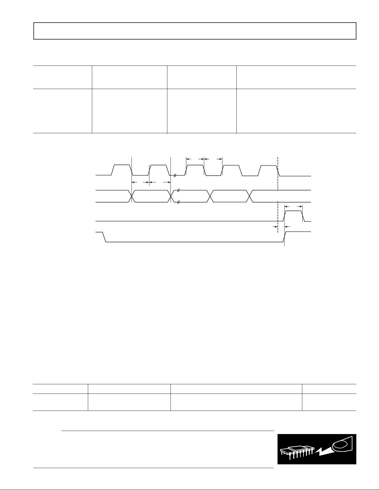
TIMING CHARACTERISTICS
4.7 k; TA = T
Parameter (B Version) Unit Test Conditions/Comments
t
1
t
2
t
3
t
4
t
5
t
6
NOTES
Guaranteed by design but not production tested.
Specifications subject to change without notice.
MIN
to T
unless otherwise noted; dBm referred to 50 .)
MAX
Limit at
T
to T
MIN
10 ns min DATA to CLOCK Set Up Time
10 ns min DATA to CLOCK Hold Time
25 ns min CLOCK High Duration
25 ns min CLOCK Low Duration
10 ns min CLOCK to LE Set Up Time
20 ns min LE Pulsewidth
CLOCK
= DVDD = 3 V 10%, 5 V 10%; AVDD ≤ VP ≤ 6.0 V ; AGND = DGND = CPGND= 0 V; R
DD
MAX
t
t
3
4
SET
=
DATA
t
DB20
(MSB)
LE
LE
t
1
2
DB19
Figure 1. Timing Diagram
ABSOLUTE MAXIMUM RATINGS
(
TA = 25°C unless otherwise noted)
1, 2
AVDD to GND3 . . . . . . . . . . . . . . . . . . . . . . . . –0.3 V to +7 V
AV
to DVDD . . . . . . . . . . . . . . . . . . . . . . . . . 0 V to + 0.3 V
DD
to GND . . . . . . . . . . . . . . . . . . . . . . . . . . . –0.3 V to +7 V
V
P
V
to AVDD . . . . . . . . . . . . . . . . . . . . . . . . . . –0.3 V to +5.5 V
P
Digital I/O Voltage to GND . . . . . . . . . –0.3 V to V
Analog I/O Voltage to GND . . . . . . . . . . –0.3 V to V
REF
, RFINA, RFINB to GND . . . . . . . –0.3 V to VDD + 0.3 V
IN
RF
INA
to RF
. . . . . . . . . . . . . . . . . . . . . . . . . . . . . ± 320 mV
INB
+ 0.3 V
DD
+ 0.3 V
P
Operating Temperature Range
Industrial (B Version) . . . . . . . . . . . . . . . . –40°C to +85°C
Storage Temperature Range . . . . . . . . . . . . –65°C to +150°C
Maximum Junction Temperature . . . . . . . . . . . . . . . . . .150°C
DB2
(CONTROL BIT C2)
TSSOP θ
CSP θ
JA
CSP θ
JA
DB1
Thermal Impedance . . . . . . . . . . . . . . 150.4°C/W
JA
Thermal Impedance (Paddle Soldered) . . . . 122°C/W
Thermal Impedance (Paddle Not Soldered) . . 216°C/W
DB0 (LSB)
(CONTROL BIT C1)
t
5
t
6
Lead Temperature, Soldering
Vapor Phase (60 sec) . . . . . . . . . . . . . . . . . . . . . . . . . 215°C
Infrared (15 sec) . . . . . . . . . . . . . . . . . . . . . . . . . . . . . 220°C
NOTES
1
Stresses above those listed under Absolute Maximum Ratings may cause perma-
nent damage to the device. This is a stress rating only; functional operation of the
device at these or any other conditions above those listed in the operational
sections of this specification is not implied. Exposure to absolute maximum rating
conditions for extended periods may affect device reliability.
2
This device is a high-performance RF integrated circuit with an ESD rating of
< 2 kΩ and it is ESD sensitive. Proper precautions should be taken for handling
and assembly.
3
GND = AGND = DGND = 0 V.
ORDERING GUIDE
Model Temperature Range Package Description Package Option
ADF4001BRU –40°C to +85°C Thin Shrink Small Outline Package (TSSOP) RU-16
ADF4001BCP –40°C to +85°C Chip Scale Package* CP-20
*Contact factory for chip availability.
CAUTION
ESD (electrostatic discharge) sensitive device. Electrostatic charges as high as 4000 V readily
accumulate on the human body and test equipment and can discharge without detection. Although
the ADF4001 features proprietary ESD protection circuitry, permanent damage may occur on
devices subjected to high-energy electrostatic discharges. Therefore, proper ESD precautions are
recommended to avoid performance degradation or loss of functionality.
REV. 0
–3–

ADF4001
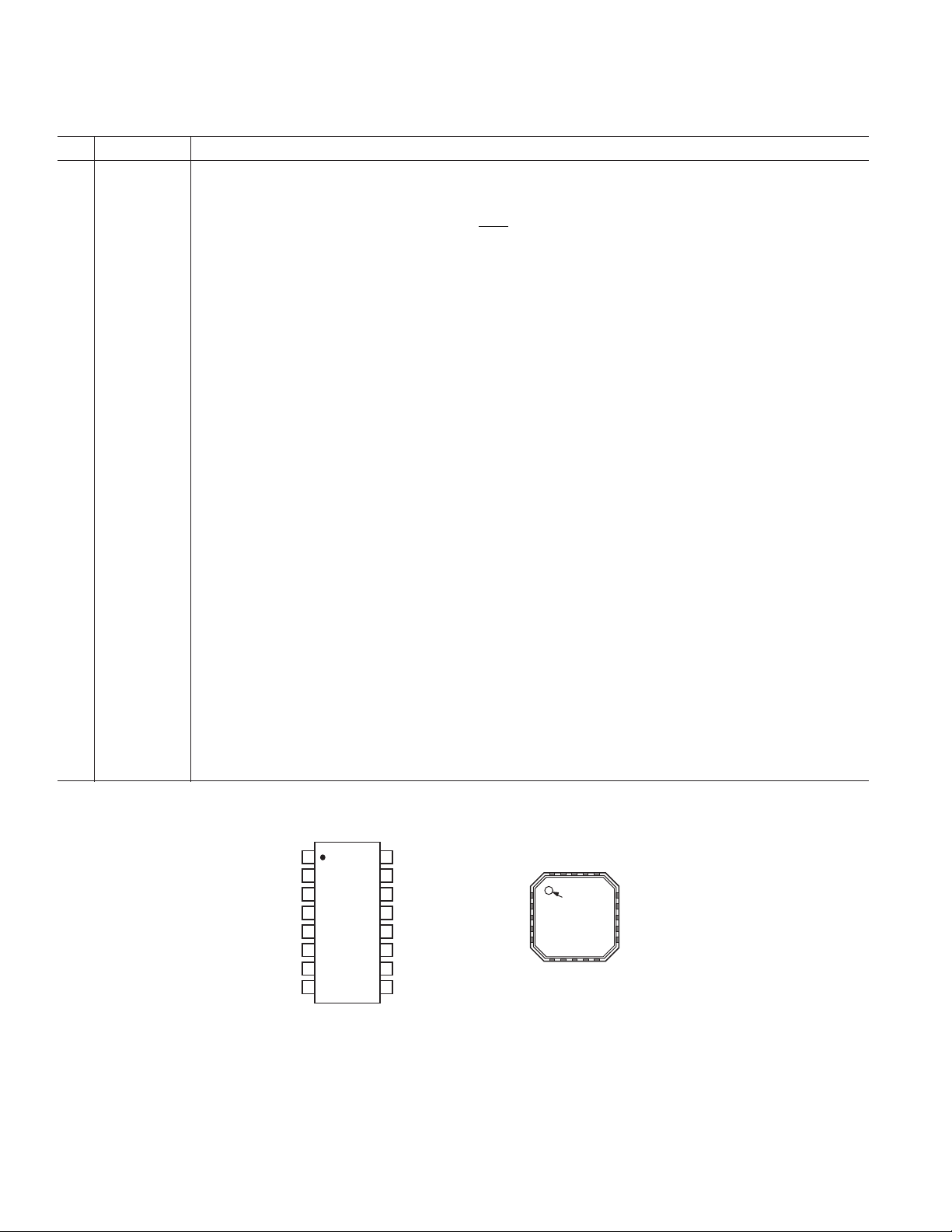
PIN FUNCTION DESCRIPTIONS
Pin Mnemonic Function
1R
SET
2 CP Charge Pump Output. When enabled, this provides ±I
3 CPGND Charge Pump Ground. This is the ground return path for the charge pump.
4 AGND Analog Ground. This is the ground return path of the prescaler.
5RF
6RF
7AV
8 REF
B Complementary Input to the N Counter. This point must be decoupled to the ground plane with a small
IN
A Input to the N Counter. This small signal input is ac-coupled to the external VCO or VCXO.
IN
DD
IN
9 DGND Digital Ground
10 CE Chip Enable. A logic low on this pin powers down the device and puts the charge pump output into three-
11 CLK Serial Clock Input. This serial clock is used to clock in the serial data to the registers. The data is latched into
12 DATA Serial Data Input. The serial data is loaded MSB first with the two LSBs being the control bits. This input is
13 LE Load Enable, CMOS Input. When LE goes high, the data stored in the shift registers is loaded into one of
14 MUXOUT This multiplexer output allows either the Lock Detect, the scaled RF, or the scaled Reference Frequency to
15 DV
16 V
DD
P
Connecting a resistor between this pin and CPGND sets the maximum charge pump output current. The
nominal voltage potential at the R
So, with R
= 4.7 kΩ, I
SET
CP MAX
SET
= 5 mA.
pin is 0.66 V. The relationship between ICP and R
I
CP AX
23 5.
=
M
R
SET
to the external loop filter which, in turn, drives the
CP
SET
is
external VCO or VCXO.
bypass capacitor, typically 100 pF. See Figure 3.
Analog Power Supply. This may range from 2.7 V to 5.5 V. Decoupling capacitors to the analog ground
plane should be placed as close as possible to this pin. AV
must be the same value as DV
DD
DD.
Reference Input. This is a CMOS input with a nominal threshold of VDD/2 and a dc equivalent input resistance of 100 kΩ. See Figure 2. This input can be driven from a TTL or CMOS crystal oscillator or can be
ac-coupled.
state mode. Taking the pin high will power up the device, depending on the status of the power-down bit F2.
the 24-bit shift register on the CLK rising edge. This input is a high-impedance CMOS input.
a high-impedance CMOS input.
the four latches, the latch being selected using the control bits.
be accessed externally.
Digital Power Supply. This may range from 2.7 V to 5.5 V. Decoupling capacitors to the digital ground plane
should be placed as close as possible to this pin. DV
must be the same value as AVDD.
DD
Charge Pump Power Supply. This should be greater than or equal to VDD. In systems where VDD is 3 V, it
can be set to 5 V and used to drive a VCO or VCXO with a tuning range of up to 5 V.
TRANSISTOR COUNT
6425 (CMOS) and 50 (Bipolar).
R
SET
CP
CPGND
AGND
RF
IN
RF
IN
AV
REF
B
A
DD
IN
1
2
ADF4001
3
4
TOP VIEW
5
(Not to Scale)
6
7
8
PIN CONFIGURATIONS
V
16
P
DV
15
DD
MUXOUT
14
13
12
11
10
9
LE
DATA
CLK
CE
DGND
CPGND 1
AGND 2
AGND 3
RFINB 4
A 5
RF
IN
–4–
SET
20 CP
19 R
18 VP17 DVDD16 DV
PIN 1
INDICATOR
ADF4001
TOP VIEW
6
7
8
IN
DD
DD
AV
AV
REF
DD
DGND 9
DGND 10
15 MUXOUT
14 LE
13 DATA
12 CLK
11 CE
REV. 0

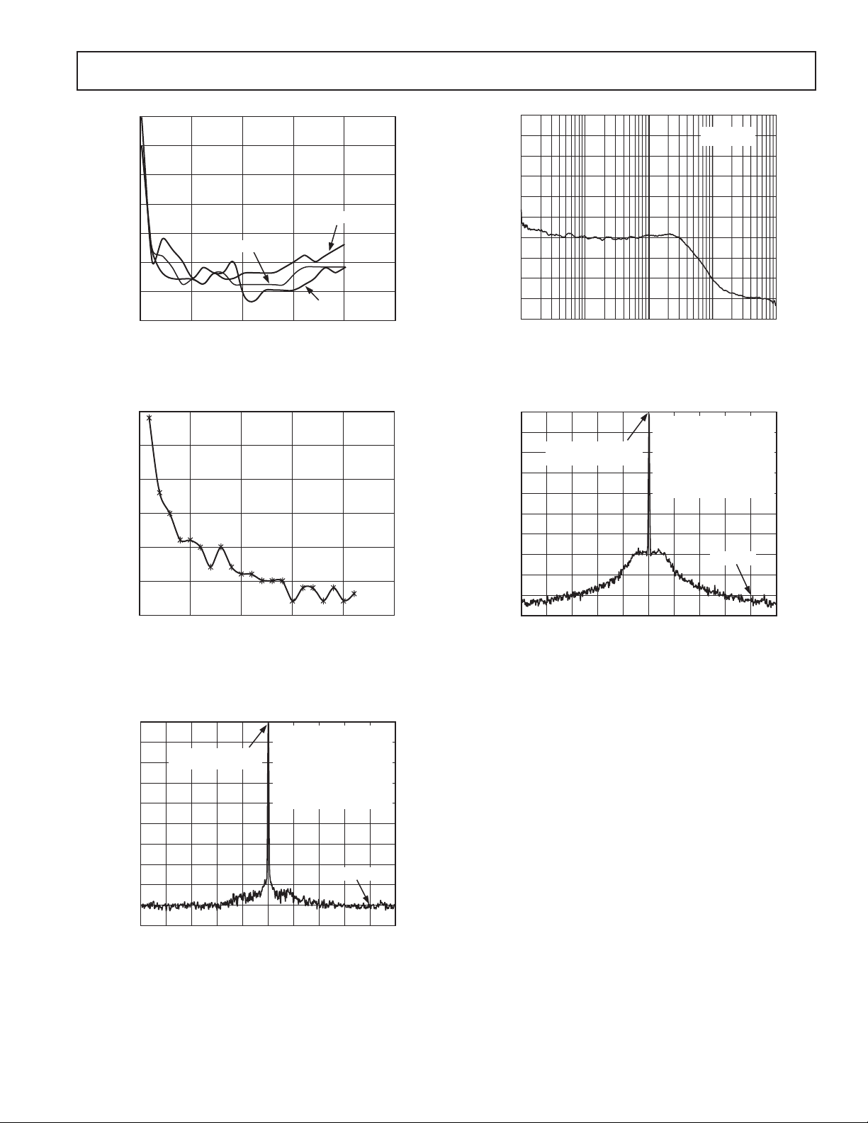
Typical Performance Characteristics–ADF4001
0
–5
–10
–15
–20
AMPLITUDE – dBm
–25
–30
–35
0
TA = +25C
50 100 150 200 250
FREQUENCY – MHz
TPC 1. Input Sensitivity. V
0
–5
–10
–15
–20
AMPLITUDE – dBm
–25
–30
0
5 10152025
FREQUENCY – MHz
TPC 2. Input Sensitivity. V
TA = +85C
TA = –40C
= 3.3 V; 100 pF on RF
DD
= 3.3 V; 100 pF on RF
DD
10dB/DIVISION R
–40
–50
–60
–70
–80
–90
–100
–110
PHASE NOISE – dBc/Hz
–120
–130
–140
100
FREQUENCY OFFSET FROM 200MHz CARRIER – Hz
IN
IN
TPC 4. Integrated Phase Noise (200 MHz, 200 kHz, 20 kHz)
0
–10
REFERENCE LEVEL =
–200kHz –100kHz 0200MHz 100kHz 200kHz
OUTPUT POWER – dB
–100
–20
–30
–40
–50
–60
–70
–80
–90
TPC 5. Reference Spurs (200 MHz, 200 kHz, 20 kHz)
= –40dBc/Hz rms NOISE = 0.229 DEGREES
L
0.229 rms
1k 10k 100k 1M
VDD = 3V, VP = 5V
= 2.5mA
I
CP
PFD FREQUENCY = 200kHz
–5.7dBm
LOOP BANDWIDTH = 20kHz
RES. BANDWIDTH = 300Hz
VIDEO BANDWIDTH = 300Hz
SWEEP = 4.2 SECONDS
AVERAGES = 20
–92.3dBc
0
–10
–20
–30
–40
–50
–60
–70
OUTPUT POWER – dB
–80
–90
–100
REFERENCE LEVEL =
–5.7dBm
–2kHz –1kHz 200MHz 1kHz 2kHz 0
VDD = 3V, VP = 5V
= 2.5mA
I
CP
PFD FREQUENCY = 200kHz
LOOP BANDWIDTH = 20kHz
RES. BANDWIDTH = 10Hz
VIDEO BANDWIDTH = 10Hz
SWEEP = 1.9 SECONDS
AVERAGES = 26
TPC 3. Phase Noise (200 MHz, 200 kHz, 20 kHz)
REV. 0
–99.2dBc/Hz
–5–
 Loading...