

Improved Second Source
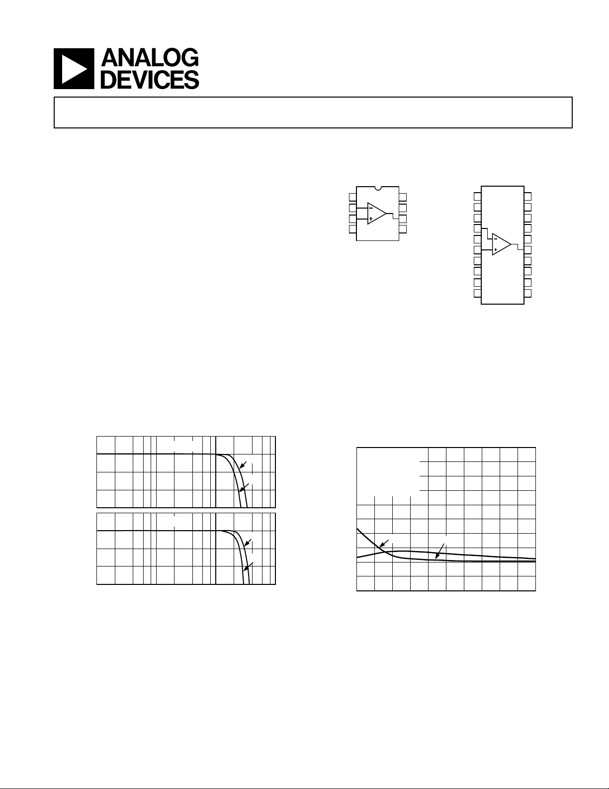
SUPPLY VOLTAGE – V
0.10
515
DIFFERENTIAL GAIN – %
0.08
0.06
0.04
0.02
0
0.09
0.07
0.05
0.03
0.01
67891011121314
0.20
DIFFERENTIAL PHASE – Degrees
0.16
0.12
0.08
0.04
0
0.18
0.14
0.10
0.06
0.02
GAIN = +2
R
F
= 750
R
L
= 150
f
C
= 3.58MHz
100 IRE
MODULATED RAMP
GAIN
PHASE
to the EL2020
ADEL2020
FEATURES
Ideal for Video Applications
0.02% Differential Gain
0.04 Differential Phase
0.1 dB Bandwidth to 25 MHz (G = +2)
High Speed
90 MHz Bandwidth (–3 dB)
500 V/s Slew Rate
60 ns Settling Time to 0.1% (V
= 10 V Step)
O
Low Noise
2.9 nV/√Hz Input Voltage Noise
Low Power
6.8 mA Supply Current
2.1 mA Supply Current (Power-Down Mode)
High Performance Disable Function
Turn-Off Time of 100 ns
Input to Output Isolation of 54 dB (Off State)
GENERAL DESCRIPTION
The ADEL2020 is an improved second source to the EL2020.
This op amp improves on all the key dynamic specifications
while offering lower power and lower cost. The ADEL2020
offers 50% more bandwidth and gain flatness of 0.1 dB to
beyond 25 MHz. In addition, differential gain and phase are
less than 0.05% and 0.05° while driving one back terminated
cable (150 Ω).
+0.1
0
–0.1
RL = 150
15V
5V
CONNECTION DIAGRAMS
8-Lead PDIP (N) 20-Lead SOIC (R)
BAL
–IN
+IN
V–
1
2
3
4
ADEL2020
TOP VIEW
8
DISABLE
7
V+
OUTPUT
6
BAL
5
1
2
BAL
ADEL2020
TOP VIEW
3
4
–IN
5
6
+IN
7
8
V–
9
10
NC = NO CONNECT
20
NCNC
19
DISABLE
18
NCNC
17
V+
16
NCNC
15
OUTPUT
14
NCNC
13
BAL
12
NCNC
11
NCNC
The ADEL2020 offers other significant improvements. The
most important is lower power supply current (33% less than the
competition) with higher output drive. Important specifications
like voltage noise and offset voltage are less than half of those
for the EL2020. The ADEL2020 also provides an improved
disable feature. The disable time (to high output impedance) is
100 ns with guaranteed break before make. The ADEL2020 is
offered for the industrial temperature range of –40°C to +85°C
and comes in both PDIP and SOIC packages.
+0.1
0
NORMALIZED GAIN – dB
–0.1
100k 1M 10M 100M
Figure 1. Fine-Scale Gain (Normalized) vs. Frequency
for Various Supply Voltages, RF = 750 Ω, Gain = +2
REV. A
Information furnished by Analog Devices is believed to be accurate and
reliable. However, no responsibility is assumed by Analog Devices for its
use, nor for any infringements of patents or other rights of third parties that
may result from its use. No license is granted by implication or otherwise
under any patent or patent rights of Analog Devices. Trademarks and
registered trademarks are the property of their respective companies.
RL = 1k
FREQUENCY – Hz
15V
5V
Figure 2. Differential Gain and Phase vs. Supply Voltage
One Technology Way, P.O. Box 9106, Norwood, MA 02062-9106, U.S.A.
Tel: 781/329-4700 www.analog.com
Fax: 781/326-8703 © 2003 Analog Devices, Inc. All rights reserved.

ADEL2020–SPECIFICATIONS
(@ TA = 25C, VS = 15 V dc, RL = 150 Ω, unless otherwise noted.)
ADEL2020A
Parameter Conditions Temperature Min Typ Max Unit
INPUT OFFSET VOLTAGE 1.5 7.5 mV
to T
T
MIN
MAX
2.0 10.0 mV
Offset Voltage Drift 7 µV/°C
COMMON-MODE REJECTION V
V
OS
±Input Current T
POWER SUPPLY REJECTION V
V
OS
±Input Current T
INPUT BIAS CURRENT –Input T
= ±10 V
CM
= ±4.5 V to ±18 V
S
+Input T
T
to T
MIN
MIN
T
MIN
MIN
MIN
MIN
to T
to T
to T
to T
to T
MAX
MAX
MAX
MAX
MAX
MAX
50 64 dB
0.1 1.0 µA/V
65 72 dB
0.05 0.5 µA/V
0.5 7.5 µA
115µA
INPUT CHARACTERISTICS
+Input Resistance 1 10 MΩ
–Input Resistance 40 Ω
+Input Capacitance 2pF
OPEN-LOOP TRANSRESISTANCE V
OPEN-LOOP DC VOLTAGE GAIN R
OUTPUT VOLTAGE SWING R
= ±10 V
O
RL = 400 Ω T
= 400 Ω, V
L
RL = 100 Ω, V
= 400 Ω T
L
= ±10 V T
OUT
= ±2.5 V T
OUT
MIN
MIN
MIN
MIN
to T
to T
to T
to T
MAX
MAX
MAX
MAX
1 3.5 MΩ
80 100 dB
76 88 dB
±12.0 ±13.0 V
Short-Circuit Current 150 mA
Output Current T
MIN
to T
MAX
30 60 mA
POWER SUPPLY
Operating Range ±3.0 ±18 V
Quiescent Current T
Power-Down Current T
Disable Pin Current Disable Pin = 0 V T
Min Disable Pin Current to Disable T
MIN
MIN
MIN
MIN
to T
to T
to T
to T
MAX
MAX
MAX
MAX
6.8 10.0 mA
2.1 3.0 mA
290 400 µA
30 µA
DYNAMIC PERFORMANCE
3 dB Bandwidth G = +1; R
G = +2; R
G = +10; R
0.1 dB Bandwidth G = +2; R
Full Power Bandwidth V
Slew Rate R
= 20 V p-p,
O
= 400 Ω 8 MHz
R
L
= 400 Ω, G = +1 500 V/µs
L
= 820 90 MHz
FB
= 750 70 MHz
FB
= 680 30 MHz
FB
= 750 25 MHz
FB
Settling Time to 0.1% 10 V Step, G = –1 60 ns
Differential Gain f = 3.58 MHz 0.02 %
Differential Phase f = 3.58 MHz 0.04 Degree
INPUT VOLTAGE NOISE f = 1 kHz 2.9 nV/√Hz
INPUT CURRENT NOISE –I
, f = 1 kHz 13 pA/√Hz
IN
+IIN, f = 1 kHz 1.5 pA/√Hz
OUTPUT RESISTANCE Open Loop (5 MHz) 15 Ω
Specifications subject to change without notice.
REV. A–2–
ADEL2020
ABSOLUTE MAXIMUM RATINGS
Supply Voltage . . . . . . . . . . . . . . . . . . . . . . . . . . . . . . . . ± 18 V
Internal Power Dissipation
2
. . . . . . . Observe Derating Curves
1
Output Short Circuit Duration . . . . Observe Derating Curves
Common-Mode Input Voltage . . . . . . . . . . . . . . . . . . . . . ± V
S
Differential Input Voltage . . . . . . . . . . . . . . . . . . . . . . . . ±6 V
Storage Temperature Range
PDIP and SOIC . . . . . . . . . . . . . . . . . . . . . –65°C to +125°C
Operating Temperature Range . . . . . . . . . . . –40°C to +85°C
Lead Temperature Range (Soldering 60 sec) . . . . . . . . . 300°C
NOTES
1
Stresses above those listed under Absolute Maximum Ratings may cause permanent damage to the device. This is a stress rating only and functional operation of
the device at these or any other conditions above those indicated in the operational
section of this specification is not implied. Exposure to absolute maximum rating
conditions for extended periods may affect device reliability.
2
8-Lead PDIP: θJA = 90°C/W
20-Lead SOIC Package: θJA = 150°C/W
+V
S
0.1F
10k
7
1
2
–
ADEL2020
3
+
5
6
4
0.1F
–V
S
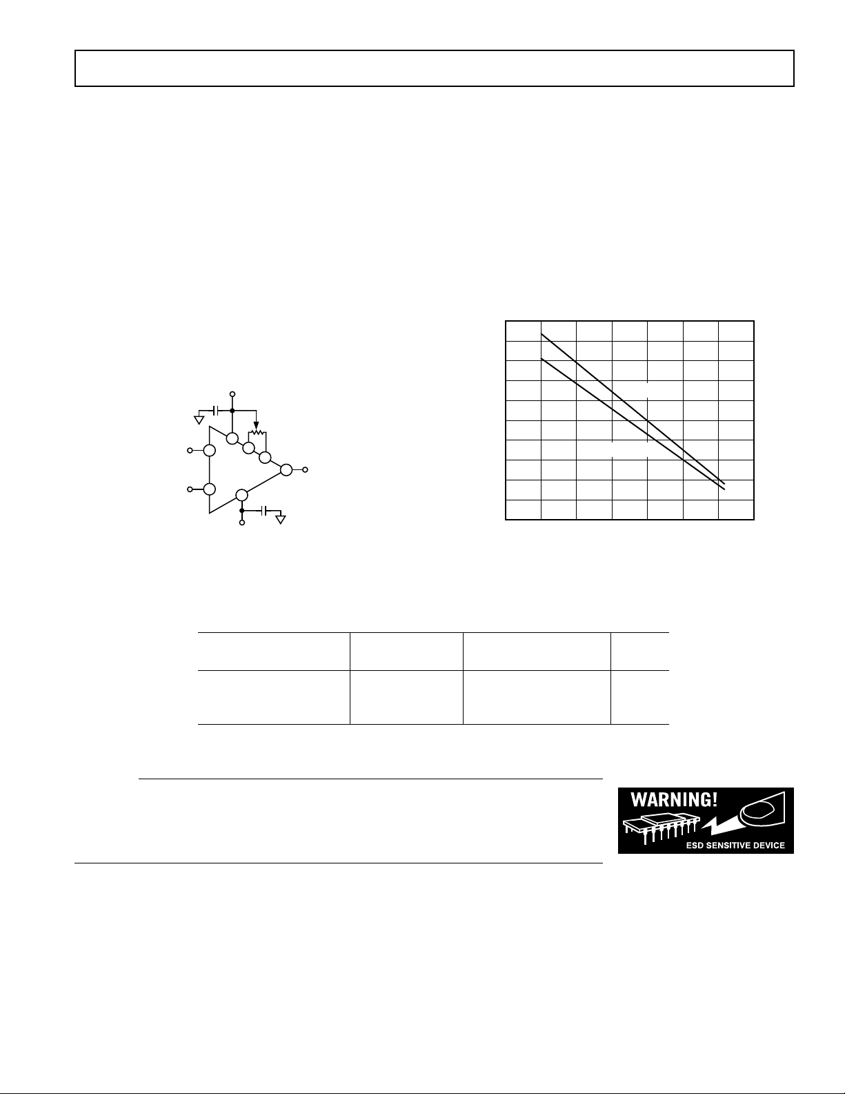
Figure 3. Offset Null Configuration
MAXIMUM POWER DISSIPATION
The maximum power that can be safely dissipated by the
ADEL2020 is limited by the associated rise in junction temperature. For the plastic packages, the maximum safe junction
temperature is 145°C. If the maximum is exceeded momentarily, proper circuit operation will be restored as soon as the
die temperature is reduced. Leaving the device in the overheated condition for an extended period can result in device
burnout. To ensure proper operation, it is important to observe
the derating curves in figure 4.
While the ADEL2020 is internally short circuit protected, this
may not be sufficient to guarantee that the maximum junction
temperature is not exceeded under all conditions.
2.4
2.2
2.0
1.8
1.6
1.4
1.2
1.0
0.8
TOTA L POWER DISSIPATION – W
0.6
0.4
–20 0 20 406080
–40 100
AMBIENT TEMPERATURE – C
20-LEAD SOIC
8-LEAD PDIP
Figure 4. Maximum Power Dissipation vs. Temperature
ORDERING GUIDE
Temperature Package Package
Model Range Description Option
ADEL2020AN –40°C to +85°C 8-Lead PDIP N-8
ADEL2020AR-20 –40°C to +85°C 20-Lead SOIC R-20
ADEL2020AR-20-REEL –40°C to +85°C 20-Lead SOIC R-20
CAUTION
ESD (electrostatic discharge) sensitive device. Electrostatic charges as high as 4000 V readily
accumulate on the human body and test equipment and can discharge without detection. Although the
ADEL2020 features proprietary ESD protection circuitry, permanent damage may occur on devices
subjected to high energy electrostatic discharges. Therefore, proper ESD precautions are recommended
to avoid performance degradation or loss of functionality.
REV. A
–3–
ADEL2020–Typical Performance Characteristics
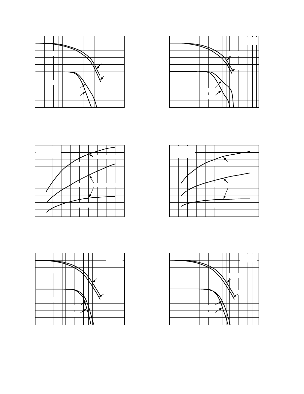
GAIN = +1
= 150
R
L
PHASE
1
0
–1
–2
CLOSED-LOOP GAIN – dB
–3
–4
–5
GAIN
V
= 15V
S
5V
1 1000
10 100
FREQUENCY – MHz
VS = 15V
5V
TPC 1. Closed-Loop Gain and Phase vs. Frequency,
G = + 1, R
110
100
–3dB BANDWIDTH – MHz
= 150 Ω, RF = 1 kΩ for ±15 V, 910 Ω for ±5 V
L
GAIN = +1
= 150
R
L
= 250mV p-p
V
O
90
80
70
60
50
40
30
20
10
24681012141618
020
RF = 750
= 1k
R
F
= 1.5k
R
F
SUPPLY VOLTAGE – V
PEAKING < 1.0dB
PEAKING < 0.1dB
TPC 2. –3 dB Bandwidth vs. Supply Voltage,
Gain = +1, RL = 150
Ω
0
–45
–90
–135
–180
–225
–270
PHASE SHIFT – Degrees
PHASE
1
0
–1
–2
CLOSED-LOOP GAIN – dB
–3
–4
–5
GAIN
1 1000
TPC 4. Closed-Loop Gain and Phase vs. Frequency,
G = +1, R
110
100
–3dB BANDWIDTH – MHz
= 1 kΩ, RF = 1 kΩ for ±15 V, 910 Ω for ±5 V
L
GAIN = –1
= 150
R
L
= 250mV p-p
V
O
90
80
70
60
50
40
30
20
10
24681012141618
020
TPC 5. –3 dB Bandwidth vs. Supply Voltage,
Gain = –1, RL = 150
V
= 15V
S
5V
10 100
FREQUENCY – MHz
RF = 499
= 681
R
F
= 1k
R
F
SUPPLY VOLTAGE – V
Ω
GAIN = +1
= 1k
R
L
VS = 15V
5V
PEAKING < 1.0dB
PEAKING < 0.1dB
0
–45
–90
–135
–180
–225
–270
PHASE SHIFT – Degrees
GAIN = –1
R
= 150
L
PHASE
VS = 15V
1
0
–1
–2
CLOSED-LOOP GAIN – dB
–3
–4
–5
GAIN
V
= 15V
S
5V
1 1000
10 100
FREQUENCY – MHz
5V
180
135
90
45
0
–45
TPC 3. Closed-Loop Gain and Phase vs. Frequency,
G = –1, RL = 150 Ω, RF = 680 Ω for ±15 V, 620 Ω for ±5 V
–1
PHASE SHIFT – Degrees
–2
CLOSED-LOOP GAIN – dB
–3
–4
–5
TPC 6. Closed-Loop Gain and Phase vs. Frequency,
G = –1, RL = 1 kΩ, RF = 680 Ω for VS = ±15 V, 620
for ±5 V
GAIN = –1
R
= 1k
L
PHASE
VS = 15V
1
0
GAIN
V
= 15V
S
5V
1 1000
10 100
FREQUENCY – MHz
5V
180
135
90
45
0
–45
PHASE SHIFT – Degrees
Ω
REV. A–4–

ADEL2020
GAIN = +2
= 150
R
L
PHASE
VS = 15V
7
6
5
4
CLOSED-LOOP GAIN – dB
3
2
1
GAIN
V
= 15V
S
5V
1 1000
10 100
FREQUENCY – MHz
5V
TPC 7. Closed-Loop Gain and Phase vs. Frequency,
G = +2, R
= 150 Ω, RF = 750 Ω for ±15 V, 715 Ω for ±5 V
L
110
GAIN = +2
= 150
R
L
100
= 250mV p-p
V
O
90
80
70
60
50
40
–3dB BANDWIDTH – MHz
30
20
10
24681012141618
020
RF = 500
SUPPLY VOLTAGE – V
= 750
R
F
R
F
= 1k
PEAKING < 1.0dB
PEAKING < 0.1dB
TPC 8. –3 dB Bandwidth vs. Supply Voltage,
Gain = +2, RL = 150
Ω
0
–45
–90
–135
–180
–225
–270
PHASE SHIFT – Degrees
PHASE
7
6
5
4
CLOSED-LOOP GAIN – dB
3
2
1
GAIN
1 1000
TPC 10. Closed-Loop Gain and Phase vs. Frequency,
G = +2, R
= 1 kΩ, RF = 750 Ω for ±15 V, 715 Ω for ±5 V
L
110
GAIN = +10
= 150
R
L
100
= 250mV p-p
V
O
90
80
70
60
50
40
–3dB BANDWIDTH – MHz
30
20
10
24681012141618
020
TPC 11. –3 dB Bandwidth vs. Supply Voltage,
Gain = +10, RL = 150
V
= 15V
S
5V
10 100
FREQUENCY – MHz
RF = 232
= 442
R
F
= 1k
R
F
SUPPLY VOLTAGE – V
Ω
GAIN = +2
= 1k
R
L
VS = 15V
5V
PEAKING < 0.5dB
PEAKING < 0.1dB
0
–45
–90
–135
–180
–225
–270
PHASE SHIFT – Degrees
GAIN = +10
R
= 270
F
= 150
R
L
PHASE
21
20
19
18
CLOSED-LOOP GAIN – dB
17
16
15
GAIN
V
= 15V
S
5V
1 1000
10 100
FREQUENCY – MHz
VS = 15V
5V
TPC 9. Closed-Loop Gain and Phase vs. Frequency,
G = +10, RL = 150 k
Ω
REV. A
0
–45
–90
–135
–180
–225
–270
PHASE SHIFT – Degrees
–5–
GAIN = +10
R
= 270
F
= 1k
R
L
PHASE
21
20
19
18
CLOSED-LOOP GAIN – dB
17
16
15
GAIN
V
= 15V
S
5V
1 1000
10 100
FREQUENCY – MHz
VS = 15V
5V
TPC 12. Closed-Loop Gain and Phase vs. Frequency, G = +10, RL = 1 k
Ω
0
–45
–90
–135
–180
–225
–270
PHASE SHIFT – Degrees

ADEL2020
30
V
= 15V
S
25
20
OUTPUT LEVEL FOR 3% THD
15
10
OUTPUT VOLTAGE – V p-p
5
0
100k 100M
VS = 5V
1M 10M
FREQUENCY – Hz
TPC 13. Maximum Undistorted Output Voltage
vs. Frequency
80
RF = 715
= +2
A
V
70
60
50
40
VS = 15V
VS = 5V
10
GAIN = +2
= 715
R
F
V
= 5V
S
1
VS = 15V
0.1
CLOSED-LOOP OUTPUT RESISTANCE –
0.01
10k 100M
100k
1M 10M
FREQUENCY – Hz
TPC 16. Closed-Loop Output Resistance vs. Frequency
10
9
V
= 15V
S
8
7
VS = 5V
30
CURVES ARE FOR WORST-CASE
CONDITION WHERE ONE
20
SUPPLY IS VARIED WHILE THE
OTHER IS HELD CONSTANT
POWER SUPPLY REJECTION – dB
10
0
10k 100M
100k
1M 10M
FREQUENCY – Hz
TPC 14. Power Supply Rejection vs. Frequency
100
VS = 5V TO 15V
INVERTING INPUT
CURRENT
10
VOLTA G E NOISE – nV/ Hz
1
10 100k
100
FREQUENCY – Hz
VOLTA GE NOISE
NONINVERTING
INPUT CURRENT
1k 10k
100
10
1
6
SUPPLY CURRENT – mA
5
4
–40 –20 0 20 40 60 80 100 120
–60 140
JUNCTION TEMPERATURE – C
TPC 17. Supply Current vs. Junction Temperature
1200
RL = 400
1100
1000
900
800
700
600
SLEW RATE – V/s
CURRENT NOISE – pA/ Hz
500
400
300
200
020
24681012141618
GAIN = –10
GAIN = +10
GAIN = +2
SUPPLY VOLTAGE – V
TPC 15. Input Voltage and Current Noise vs. Frequency
TPC 18. Slew Rate vs. Supply Voltage
REV. A–6–

ADEL2020
1k
+V
S
0.1F
7
2
–
S
0.1F
6
R
L
ADEL2020
V
IN
3
+
R
T
4
–V
Figure 5. Connection Diagram for A
681
+V
S
0.1F
681
V
IN
2
–
ADEL2020
3
+
7
6
4
0.1F
–V
S
R
Figure 6. Connection Diagram for A
750
+V
S
0.1F
750
V
O
V
IN
R
T
= +1
VCL
V
O
L
= –1
VCL
Figure 7. Connection Diagram for A
30
V
IN
R
T
Figure 8. Connection Diagram for A
2
–
ADEL2020
3
+
270
2
–
ADEL2020
3
+
7
6
4
0.1F
–V
S
+V
S
0.1F
7
6
4
0.1F
–V
S
V
O
R
L
= +2
VCL
V
O
R
L
= +10
VCL
REV. A
–7–

ADEL2020
GENERAL DESIGN CONSIDERATIONS
The ADEL2020 is a current feedback amplifier optimized for
use in high performance video and data acquisition systems.
Since it uses a current feedback architecture, its closed-loop
bandwidth depends on the value of the feedback resistor. The
–3 dB bandwidth is also somewhat dependent on the power
supply voltage. Lowering the supplies increases the values of
internal capacitances, reducing the bandwidth. To compensate for this, smaller values of feedback resistors are used at
lower supply voltages.
POWER SUPPLY BYPASSING
Adequate power supply bypassing can be critical when optimizing the performance of a high frequency circuit. Inductance in
the power supply leads can contribute to resonant circuits that
produce peaking in the amplifier’s response. In addition, if large
current transients must be delivered to the load, then bypass
capacitors (typically greater than 1 µF) will be required to
provide the best settling time and lowest distortion. Although
the recommended 0.1 µF power supply bypass capacitors will
be sufficient in most applications, more elaborate bypassing
(such as using two paralleled capacitors) may be required in
some cases.
CAPACITIVE LOADS
When used with the appropriate feedback resistor, the ADEL2020
can drive capacitive loads exceeding 1000 pF directly without
oscillation. Another method of compensating for large load
capacitance is to insert a resistor in series with the loop output.
In most cases, less than 50 Ω is all that is needed to achieve an
extremely flat gain response.
OFFSET NULLING
A 10 kΩ pot connected between Pins 1 and 5, with its wiper connected to V+, can be used to trim out the inverting input current
(with about ±20 µA of range). For closed-loop gains above about
5, this may not be sufficient to trim the output offset voltage to
zero. Tie the pot’s wiper to ground through a large value resistor
(50 kΩ for ±5 V supplies, 150 kΩ for ±15 V supplies) to trim the
output to zero at high closed-loop gains.
DISABLE MODE
By pulling the voltage on Pin 8 to common (0 V), the ADEL2020
can be put into a disabled state. In this condition, the supply
current drops to less than 2.8 mA, the output becomes a high
impedance, and there is a high level of isolation from input to
output. In the case of a line driver, for example, the output
impedance will be about the same as that for a 1.5 kΩ resistor
(the feedback plus gain resistors) in parallel with a 13 pF capacitor
(due to the output), and the input to output isolation will be
better than 50 dB at 10 MHz.
Leaving the disable pin disconnected (floating) will leave the
part in the enabled state.
In cases where the amplifier is driving a high impedance load,
the input to output isolation will decrease significantly if the
input signal is greater than about 1.2 V p–p. The isolation can
be restored to the 50 dB level by adding a dummy load (say 150 Ω)
at the amplifier output. This will attenuate the feedthrough
signal. (This is not an issue for multiplexer applications where the
outputs of multiple ADEL2020s are tied together as long as at
least one channel is in the ON state.) The input impedance of
the disable pin is about 35 kΩ in parallel with a few pF. When
grounded, about 50 µA flows out of the disable pin for ±5 V supplies.
Break-before-make operation is guaranteed by design. If driven
by standard CMOS logic, the disable time (until the output is
high impedance) is about 100 ns and the enable time (to low
impedance output) is about 160 ns. Since it has an internal pullup resistor of about 35 kΩ, the ADEL2020 can be used with
open drain logic as well. In that case, the enable time increases
to about 1 µs.
If there is a nonzero voltage present on the amplifier’s output
at the time it is switched to the disabled state, some additional
decay time will be required for the output voltage to relax to
zero. The total time for the output to go to zero will normally
be about 250 ns; it is somewhat dependent on the load impedance.
OPERATION AS A VIDEO LINE DRIVER
The ADEL2020 is designed to offer outstanding performance at
closed-loop gains of 1 or greater. At a gain of 2, the ADEL2020
makes an excellent video line driver. The low differential gain
and phase errors and wide –0.1 dB bandwidth are nearly independent of supply voltage and load. For applications requiring
widest 0.1 dB bandwidth, it is recommended to use 715 Ω feed-
back and gain resistors. This will result in about 0.05 dB of
peaking and a –0.1 dB bandwidth of 30 MHz on ±15 V supplies.
REV. A–8–

OUTLINE DIMENSIONS
8-Lead Plastic Dual-in-Line Package [PDIP]
(N-8)
Dimensions shown in inches and (millimeters)
0.375 (9.53)
0.365 (9.27)
0.355 (9.02)
8
1
0.100 (2.54)
0.180
(4.57)
MAX
0.150 (3.81)
0.130 (3.30)
0.110 (2.79)
0.022 (0.56)
0.018 (0.46)
0.014 (0.36)
CONTROLLING DIMENSIONS ARE IN INCHES; MILLIMETER DIMENSIONS
(IN PARENTHESES) ARE ROUNDED-OFF INCH EQUIVALENTS FOR
REFERENCE ONLY AND ARE NOT APPROPRIATE FOR USE IN DESIGN
COMPLIANT TO JEDEC STANDARDS MO-095AA
BSC
5
4
0.295 (7.49)
0.285 (7.24)
0.275 (6.98)
0.015
(0.38)
MIN
SEATING
PLANE
0.060 (1.52)
0.050 (1.27)
0.045 (1.14)
0.325 (8.26)
0.310 (7.87)
0.300 (7.62)
0.150 (3.81)
0.135 (3.43)
0.120 (3.05)
0.015 (0.38)
0.010 (0.25)
0.008 (0.20)
ADEL2020
20-Lead Standared Small Outline Pacakge [SOIC]
Wide Body
(R-20)
Dimensions shown in millimeters and (inches)
13.00 (0.5118)
12.60 (0.4961)
20 11
1
0.30 (0.0118)
0.10 (0.0039)
1.27
COPLANARITY
0.10
CONTROLLING DIMENSIONS ARE IN MILLIMETERS; INCH DIMENSIONS
(IN PARENTHESES) ARE ROUNDED-OFF MILLIMETER EQUIVALENTS FOR
REFERENCE ONLY AND ARE NOT APPROPRIATE FOR USE IN DESIGN
(0.0500)
COMPLIANT TO JEDEC STANDARDS MS-013AC
BSC
0.51 (0.0201)
0.33 (0.0130)
7.60 (0.2992)
7.40 (0.2913)
10
2.65 (0.1043)
2.35 (0.0925)
SEATING
PLANE
10.65 (0.4193)
10.00 (0.3937)
0.32 (0.0126)
0.23 (0.0091)
0.75 (0.0295)
0.25 (0.0098)
8
0
45
1.27 (0.0500)
0.40 (0.0157)
REV. A
–9–

ADEL2020
Revision History
Location Page
1/03—Data Sheet changed from REV. 0 to REV. A.
Format updated . . . . . . . . . . . . . . . . . . . . . . . . . . . . . . . . . . . . . . . . . . . . . . . . . . . . . . . . . . . . . . . . . . . . . . . . . . . . . . . . . . .Universal
8-Lead PDIP (N) and 20-Lead SOIC (R) updated . . . . . . . . . . . . . . . . . . . . . . . . . . . . . . . . . . . . . . . . . . . . . . . . . . . . . . . .Universal
OUTLINE DIMENSIONS updated . . . . . . . . . . . . . . . . . . . . . . . . . . . . . . . . . . . . . . . . . . . . . . . . . . . . . . . . . . . . . . . . . . . . . . . . . 9
REV. A–10–

–11–

C03445–0–1/03(A)
–12–
PRINTED IN U.S.A.
 Loading...