


Polyphase Multifunction Energy Metering IC
with per Phase Active and Reactive Powers
FEATURES
Highly accurate; supports EN 50470-1, EN 50470-3,
IEC 62053-21, IEC 62053-22, and IEC 62053-23 standards
Compatible with 3-phase, 3- or 4-wire (delta or wye), and
other 3-phase services
Supplies total (fundamental and harmonic) active/reactive/
apparent energy and fundamental active/reactive energy
on each phase and on the overall system
Less than 0.1% error in active and reactive energy over a
dynamic range of 1000 to 1 at T
Less than 0.2% error in active and reactive energy over a
dynamic range of 3000 to 1 at T
Supports current transformer and di/dt current sensors
Dedicated ADC channel for neutral current input
Less than 0.1% error in voltage and current rms over a
dynamic range of 1000 to 1 at T
Supplies sampled waveform data on all three phases and on
neutral current
Selectable no load threshold levels for total and
fundamental active and reactive powers, as well as for
apparent powers
Low power battery mode monitors phase currents for
antitampering detection
Battery supply input for missing neutral operation
Phase angle measurements in both current and voltage
channels with a typical 0.3° error
Wide-supply voltage operation: 2.4 V to 3.7 V
Reference: 1.2 V (drift 10 ppm/°C typical) with external
overdrive capability
Single 3.3 V supply
40-lead lead frame chip scale package (LFCSP), Pb-free
Operating temperature: −40° to +85°C
Flexible I
2
C, SPI, and HSDC serial interfaces
APPLICATIONS
Energy metering systems
= 25°C
A
= 25°C
A
= 25°C
A
ADE7878
GENERAL DESCRIPTION
The ADE78781 is a high accuracy, 3-phase electrical energy
measurement IC with serial interfaces and three flexible pulse
outputs. The ADE7878 incorporates second-order sigma-delta
(Σ-∆) analog-to-digital converters (ADCs), a digital integrator,
reference circuitry, and all the signal processing required to
perform total (fundamental and harmonic) active, reactive, and
apparent energy measurement and rms calculations, as well as
fundamental only active and reactive energy measurement and
rms calculations. A fixed function digital signal processor (DSP)
executes this signal processing. The DSP program is stored into
internal ROM memory.
The ADE7878 is suitable for measuring active, reactive, and
apparent energy in various 3-phase configurations, such as wye
or delta services, with both three and four wires. The ADE7878
provides system calibration features for each phase, that is, rms
offset correction, phase calibration, and gain calibration. The
CF1, CF2, and CF3 logic outputs provide a wide choice of
power information: total active, reactive, and apparent powers,
or the sum of the current rms values, and fundamental active
and reactive powers.
The ADE7878 contains waveform sample registers that allow
access to all ADC outputs. The device also incorporates power
quality measurements, such as short duration low or high
voltage detections, short duration high current variations, line
voltage period measurement, and angles between phase voltages
and currents. Two serial interfaces, SPI and I
communicate with the ADE7878. A dedicated high speed
interface, the high speed data capture (HSDC) port, can be used
in conjunction with I
2
C to provide access to the ADC outputs
and real-time power information. The ADE7878 also has two
interrupt request pins,
IRQ0
and
IRQ1
enabled interrupt event has occurred. For the ADE7878, three
specially designed low power modes ensure the continuity of
energy accumulation when the ADE7878 is in a tampering
situation.
The ADE7878 is available in a 40-lead LFCSP, Pb-free package.
2
C, can be used to
, to indicate that an
1
U.S. patents pending.
Rev. 0
Information furnished by Analog Devices is believed to be accurate and reliable. However, no
responsibility is assumed by Analog Devices for its use, nor for any infrin gements of patents or other
rights of third parties that may result from its use. Specifications subject to change without notice. No
license is granted by implication or otherwise under any patent or patent rights of Analog Devices.
Trademarks and registered trademarks are the property of their respective owners.
One Technology Way, P.O. Box 9106, Norwood, MA 02062-9106, U.S.A.
Tel: 781.329.4700 www.analog.com
Fax: 781.461.3113 ©2010 Analog Devices, Inc. All rights reserved.

ADE7878
TABLE OF CONTENTS
Features .............................................................................................. 1
Applications ....................................................................................... 1
General Description ......................................................................... 1
Revision History ............................................................................... 3
Functional Block Diagram .............................................................. 4
Specifications ..................................................................................... 5
Timing Characteristics ................................................................ 8
Absolute Maximum Ratings .......................................................... 11
Thermal Resistance .................................................................... 11
ESD Caution ................................................................................ 11
Pin Configuration and Function Descriptions ........................... 12
Typical Performance Characteristics ........................................... 14
Test Circuit ...................................................................................... 17
Terminolog y .................................................................................... 18
Power Management ........................................................................ 19
PSM0—Normal Power Mode ................................................... 19
PSM1—Reduced Power Mode.................................................. 19
PSM2—Low Power Mode ......................................................... 19
PSM3—Sleep Mode .................................................................... 20
Power-Up Procedure .................................................................. 20
Hardware Reset ........................................................................... 21
Software Reset Functionality .................................................... 21
Theory of Operation ...................................................................... 24
Analog Inputs .............................................................................. 24
Analog-to-Digital Conversion .................................................. 24
Antialiasing Filter ................................................................... 25
ADC Transfer Function ......................................................... 25
Current Channel ADC ............................................................... 25
Current Waveform Gain Registers ....................................... 26
Current Channel HPF ........................................................... 26
Current Channel Sampling ................................................... 27
di/dt Curent Sensor and Digital Integrator ............................. 27
Voltage Channel ADC ................................................................ 28
Voltage Waveform Gain Registers ........................................ 28
Voltage Channel HPF ............................................................ 28
Voltage Channel Sampling .................................................... 28
Changing Phase Voltage Datapath ........................................... 29
Power Quality Measurements ................................................... 29
Zero Crossing Detection ....................................................... 29
Zero-Crossing Timeout ......................................................... 30
Phase Sequence Detection .................................................... 30
Time Interval Between Phases ............................................. 31
Period Measurement .............................................................. 32
Phase Voltage Sag Detection ................................................. 32
Peak Detection ........................................................................ 33
Overvoltage and Overcurrent Detection ............................ 34
Neutral Current Mismatch ................................................... 35
Phase Compensation ................................................................. 35
Reference Circuit ........................................................................ 37
Digital Signal Processor ............................................................. 37
Root Mean Square Measurement ............................................. 37
Current RMS Calculation ..................................................... 38
Current Mean Absolute Value Calculation ......................... 39
Voltage Channel RMS Calculation ...................................... 40
Voltage RMS Offset Compensation ..................................... 41
Active Power Calculation .......................................................... 41
Total Active Power Calculation ............................................ 41
Fundamental Active Power Calculation .............................. 43
Active Power Gain Calibration ............................................. 43
Active Power Offset Calibration .......................................... 43
Sign of Active Power Calculation ......................................... 43
Active Energy Calculation .................................................... 44
Integration Time Under Steady Load .................................. 45
Energy Accumulation Modes ............................................... 46
Line Cycle Active Energy Accumulation Mode ................. 46
Reactive Power Calculation ...................................................... 47
Reactive Power Gain Calibration ......................................... 48
Reactive Power Offset Calibration ....................................... 48
Sign of Reactive Power Calculation ..................................... 48
Reactive Energy Calculation ................................................. 49
Integration Time Under A Steady Load .............................. 51
Energy Accumulation Modes ............................................... 51
Line Cycle Reactive Energy Accumulation Mode ............. 51
Apparent Power Calculation ..................................................... 52
Apparent Power Gain Calibration ....................................... 53
Apparent Power Offset Calibration ..................................... 53
Rev. 0 | Page 2 of 92

ADE7878
Apparent Power Calculation Using VNOM ........................ 53
Apparent Energy Calculation ................................................ 53
Integration Time Under Steady Load ................................... 54
Energy Accumulation Mode .................................................. 54
Line Cycle Apparent Energy Accumulation Mode ............. 54
Waveform Sampling Mode ........................................................ 55
Energy-to-Frequency Conversion ............................................ 55
Synchronizing Energy Registers with CFx Outputs ........... 57
CF Outputs for Various Accumulation Modes ................... 57
Sign of Sum-of-Phase Powers in the CFx Datapath ........... 59
No Load Condition ..................................................................... 59
No Load Detection Based On Total Active, Reactive Powers
................................................................................................... 59
No Load Detection Based on Fundamental Active and
Reactive Powers ....................................................................... 60
No Load Detection Based on Apparent Power ................... 60
Checksum Register ..................................................................... 60
Interrupts ..................................................................................... 62
Using the Interrupts with an MCU ...................................... 62
Serial Interfaces ........................................................................... 63
Serial Interface Choice ........................................................... 63
I2C-Compatible Interface ....................................................... 63
SPI-Compatible Interface ...................................................... 65
HSDC Interface ....................................................................... 65
ADE7878 Evaluation Board ...................................................... 69
Die Version .................................................................................. 69
Registers List .................................................................................... 70
Outline Dimensions ........................................................................ 90
Ordering Guide ........................................................................... 90
REVISION HISTORY
2/10—Revision 0: Initial Version
Rev. 0 | Page 3 of 92
ADE7878
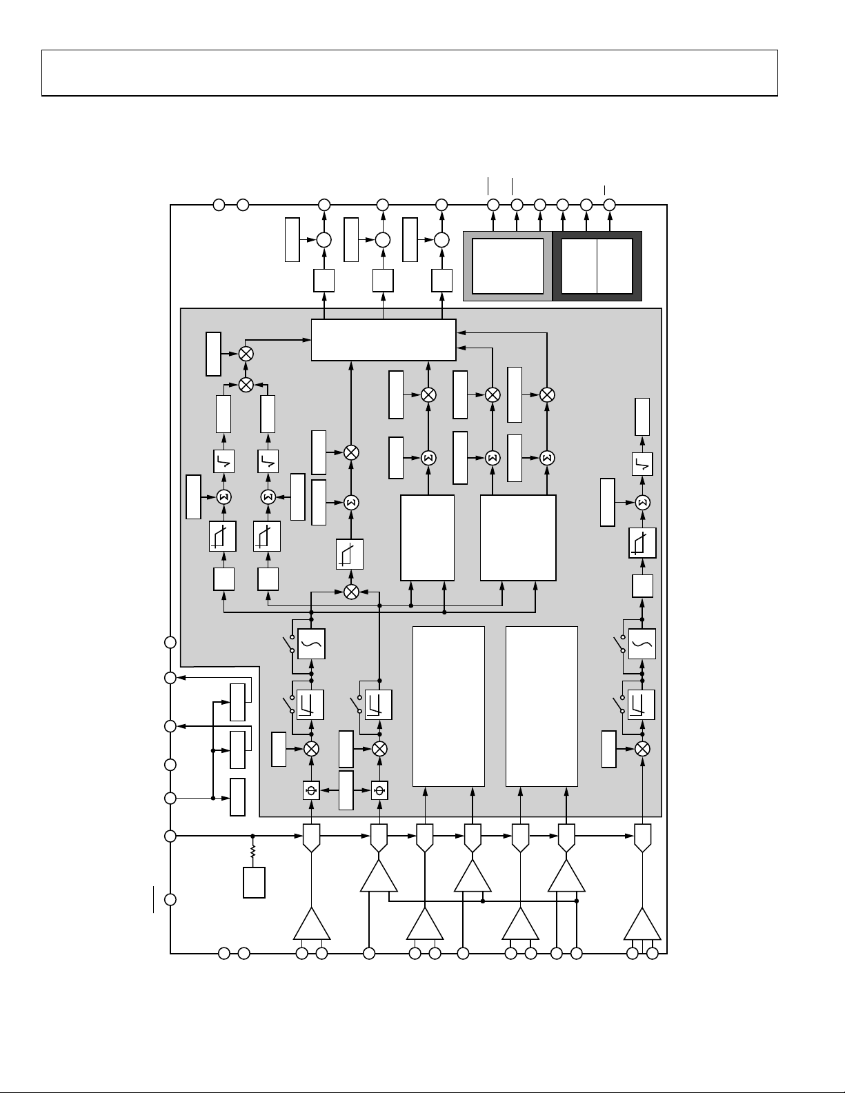
FUNCTIONAL BLOCK DIAGRAM
PM0
PM1
3
2
ADE7878
AVAGAIN
AIRMS
AIRMSOS
2
X
AVR MS
LPF
LPF
2
X
08510-201
CF1
33
:
CF1DEN
DFC
AWGAIN
AVR MSO S
AWATTO S
CF2
34
:
CF2DEN
DFC
PHASE
C DATA
A, B AND
AVARGAINAVAROS
LPF
CF3DEN
COMPUTATI ONAL
CF3/HSCLK
35
IRQ0
29
IRQ1
32
SCLK/SCL
MOSI/SDA
MISO/HSD
SS/HSA
39
37
38
36
:
C
2
COMPUTATIONAL
SPI/I
AFVARG AINAFVAROS
BLOCK FOR
ACTIVE AND
FUNDAMENTAL
REACTIVE PO WER
DFC
AFWGAINAFWATTO S
TOTAL
BLOCK FOR
REACTIVE PO WER
C
2
I
HSDC
PROCESSOR
DIGITAL SIGNAL
NIRMS
NIRMSOS
LPF
2
X
VDD AGND AVDD DVDD DGND
IN/OUT
REF
RESET
6
DIGITAL
52426 25174
27
CLKIN
INTEGRATOR
HPF
[23:0]
HPFDIS
AIGAIN
POR LDO LDO
REF
1.2V
28
CLKOUT
7
[23:0]
HPFDIS
ADC
PGA1
8
IAP
IAN
HPF
ACTIVE/REACT IVE/
AVGAINAPHCAL
ADC
PGA3
23
VAP
ADC
PGA1
9
IBP
DATA PATH)
(SEE PHASE A FO R DETAILED
RMS CALCULATI ON FOR PHASE B
APPARENT/TO TAL/F UNDAMENTAL
ENERGIES AND VO LTAGE/ CURRENT
ADC
PGA3
22
12
IBN
VBP
ACTIVE/REACT IVE/
RMS CALCULATI ON FOR PHASE C
APPARENT/TO TAL/F UNDAMENTAL
ENERGIES AND VO LTAGE/ CURRENT
ADC
PGA1
13
14
ICP
ICN
DIGITAL
INTEGRATOR
[23:0]
HPFDIS
DATA PATH)
(SEE PHASE A FO R DETAILED
ADC
PGA3
19
18
VN
VCP
HPF
NIGAIN
ADC
PGA2
15
16
INP
INN
Figure 1.
Rev. 0 | Page 4 of 92

ADE7878
SPECIFICATIONS
VDD = 3.3 V ± 10%, AGND = DGND = 0 V, on-chip reference, CLKIN = 16.384 MHz, T
MIN
to T
= −40°C to +85°C.
MAX
Table 1.
1, 2
Parameter
Min Typ Max Unit Test Conditions/Comments
ACCURACY
Active Energy Measurement
Active Energy Measurement Error
(per Phase)
Total Active Power 0.1 % Over a dynamic range of 1000 to 1, PGA = 1, 2, 4;
integrator off
0.2 % Over a dynamic range of 3000 to 1, PGA = 1, 2, 4;
integrator off
0.1 % Over a dynamic range of 500 to 1, PGA = 8, 16;
integrator on
Fundamental Active Power 0.1 % Over a dynamic range of 1000 to 1, PGA = 1, 2, 4;
integrator off
0.2 % Over a dynamic range of 3000 to 1, PGA = 1, 2, 4;
integrator off
0.1 % Over a dynamic range of 500 to 1, PGA = 8, 16;
integrator on
Phase Error Between Channels Line frequency = 45 Hz to 65 Hz, HPF on
PF = 0.8 Capacitive ±0.05 Degrees Phase lead 37°
PF = 0.5 Inductive ±0.05 Degrees Phase lag 60°
AC Power Supply Rejection VDD = 3.3 V + 120 mV rms/120 Hz, IPx = VPx =
± 100 mV rms
Output Frequency Variation 0.01 %
DC Power Supply Rejection VDD = 3.3 V ± 330 mV dc
Output Frequency Variation 0.01 %
Total Active Energy Measurement
2 kHz
Bandwidth
REACTIVE ENERGY MEASUREMENT
Reactive Energy Measurement Error
(per Phase)
Total Active Power 0.1 % Over a dynamic range of 1000 to 1, PGA = 1, 2, 4;
integrator off
0.2 % Over a dynamic range of 3000 to 1, PGA = 1, 2, 4;
integrator off
0.1 % Over a dynamic range of 500 to 1, PGA = 8, 16;
integrator on
Fundamental Active Power 0.1 % Over a dynamic range of 1000 to 1, PGA = 1, 2, 4;
integrator off
0.2 % Over a dynamic range of 3000 to 1, PGA = 1, 2, 4;
integrator off
0.1 % Over a dynamic range of 500 to 1, PGA = 8, 16;
integrator on
Phase Error Between Channels Line frequency = 45 Hz to 65 Hz, HPF on
PF = 0.8 Capacitive ±0.05 Degrees Phase lead 37°
PF = 0.5 Inductive ±0.05 Degrees Phase lag 60°
AC Power Supply Rejection VDD = 3.3 V + 120 mV rms/120 Hz, IPx = VPx =
± 100 mV rms
Output Frequency Variation 0.01 %
Rev. 0 | Page 5 of 92

ADE7878
Parameter
1, 2
Min Typ Max Unit Test Conditions/Comments
DC Power Supply Rejection VDD = 3.3 V ± 330 mV dc
Output Frequency Variation 0.01 %
Total Reactive Energy Measurement
2 kHz
Bandwidth
RMS MEASUREMENTS
I rms and V rms Measurement
2 kHz
Bandwidth
I rms and V rms Measurement Error
0.1 % Over a dynamic range of 1000 to 1, PGA = 1
(PSM0 Mode)
MEAN ABSOLUTE VALUE (MAV)
MEASUREMENT
Imav Measurement Bandwidth (PSM1
260 Hz
Mode)
Imav Measurement Error (PSM1 Mode) 0.5 % Over a dynamic range of 100 to 1, PGA = 1
ANALOG INPUTS
Maximum Signal Levels ±500 mV peak Differential inputs between the following
pins: IAP and IAN, IBP and IBN, ICP and ICN;
single-ended inputs between the following
pins: VAP and VN, VBP and VN, VCP and VN
Input Impedance (DC)
IAP, IAN, IBP, IBN, ICP, ICN, VAP, VBP,
400 kΩ
VCP Pins
VN Pin 130 kΩ
ADC Offset Error ±20 mV PGA = 1, uncalibrated error, see the
Terminology section
Gain Error ±4 % External 1.2 V reference
WAVEFORM SAMPLING Sampling CLKIN/2048, 16.384 MHz/2048 =
8 kSPS
Current and Voltage Channels See Waveform Sampling Mode section
Signal-to-Noise Ratio, SNR 70 dB PGA = 1
Signal-to-Noise-and-Distortion Ratio,
65 dB PGA = 1
SINAD
Bandwidth (−3 dB) 2 kHz
TIME INTERVAL BETWEEN PHASES
Measurement Error 0.3 Degrees Line frequency = 45 Hz to 65 Hz, HPF on
CF1, CF2, CF3 PULSE OUTPUTS
Maximum Output Frequency 8 kHz WTHR = VARTHR = VATHR = PMAX = 33,516,139
Duty Cycle 50 % If CF1, CF2, or CF3 frequency > 6.25 Hz and
CFDEN is even and > 1
(1 + 1/CFDEN)
× 50%
If CF1, CF2, or CF3 frequency > 6.25 Hz and
CFDEN is odd and > 1
Active Low Pulse Width 80 ms If CF1, CF2, or CF3 frequency < 6.25 Hz
Jitter 0.04 % For CF1, CF2, or CF3 frequency = 1 Hz and
nominal phase currents are larger than 10%
of full scale
REFERENCE INPUT
REF
Input Voltage Range 1.1 1.3 V Minimum = 1.2 V − 8%; maximum = 1.2 V + 8%
IN/OUT
Input Capacitance 10 pF
ON-CHIP REFERENCE Nominal 1.2 V at REF
pin at TA = 25°C
IN/OUT
PSM0 and PSM1 Modes
Reference Error ±0.9 mV max
Output Impedance 1.4 kΩ min
Temperature Coefficient 10 50 ppm/°C
Rev. 0 | Page 6 of 92

ADE7878
Parameter
1, 2
Min Typ Max Unit Test Conditions/Comments
CLKIN All specifications CLKIN of 16.384 MHz
Input Clock Frequency 16.384 MHz
Crystal Equivalent Series Resistance 30 50 k
CLKIN Input Capacitance 20 pF
CLKOUT Output Capacitance 20 pF
LOGIC INPUTS—MOSI/SDA, SCLK/SCL,
,
CLKIN,
SS
Input High Voltage, V
Input Low Voltage, V
, PM0, AND PM1
RESET
2.0 V VDD = 3.3 V ± 10%
INH
0.8 V VDD = 3.3 V ± 10%
INL
Input Current, IIN −7.5 µA Input = 0 V, VDD = 3.3 V
3 A Input = VDD = 3.3 V
100 nA Input = VDD = 3.3 V
Input Capacitance, CIN 10 pF
LOGIC OUTPUTS—
IRQ0, IRQ1
, MISO/HSD,
DVDD = 3.3 V ± 10%
AND CLKOUT
Output High Voltage, VOH 2.4 V VDD = 3.3 V ± 10%
I
800 µA
SOURCE
Output Low Voltage, VOL 0.4 V VDD = 3.3 V ± 10%
I
2 mA
SINK
CF1, CF2, CF3/HSCLK
Output High Voltage, V
I
500 µA
SOURCE
2.4 V VDD = 3.3 V ± 10%
OH
Output Low Voltage, VOL 0.4 V VDD = 3.3 V ± 10%
I
2 mA
SINK
POWER SUPPLY For specified performance
PSM0 Mode
VDD Pin 3.0 3.6 V Minimum = 3.3 V − 10%; maximum = 3.3 V +
10%
IDD 22 24.29 mA
PSM1 and PSM2 Modes
VDD Pin 2.4 3.7 V
IDD
PSM1 Mode 4.85 5.61 mA
PSM2 Mode 0.2 0.259 mA
PSM3 Mode For specified performance
VDD Pin 2.4 3.7 V
IDD in PSM3 Mode 1.62 A
1
See the Typical Performance Characteristics section.
2
See the Terminology section for a definition of the parameters.
Rev. 0 | Page 7 of 92
ADE7878
K
TIMING CHARACTERISTICS
VDD = 3.3 V ± 10%, AGND = DGND = 0 V, on-chip reference, CLKIN = 16.384 MHz, T
MIN
to T
= −40°C to +85°C.
MAX
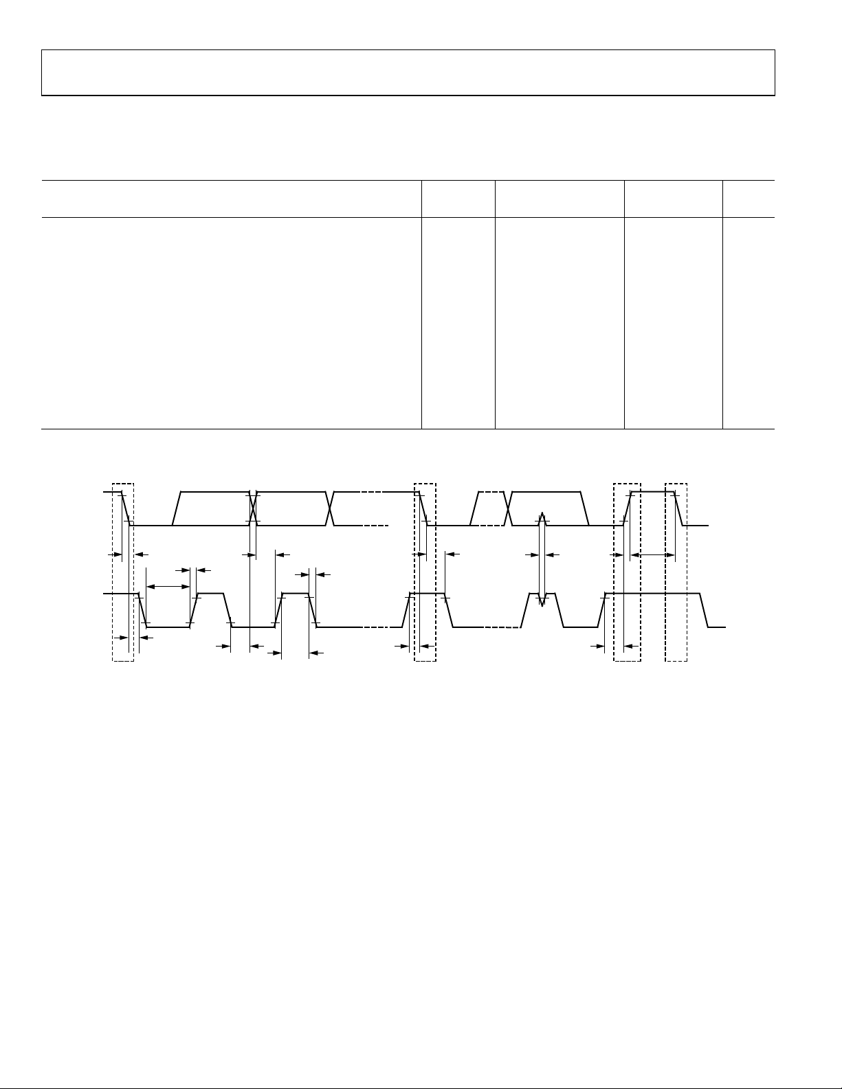
Table 2. I
2
C-Compatible Interface Timing Parameter
Standard Mode Fast Mode
Parameter Symbol Min Max Min Max Unit
SCL Clock Frequency f
Hold Time (Repeated) Start Condition t
Low Period of SCL Clock t
High Period of SCL Clock t
Set-Up Time for Repeated Start Condition t
Data Hold Time t
Data Setup Time t
0 100 0 400 kHz
SCL
4.0 0.6 s
HD;STA
4.7 1.3 µs
LOW
4.0 0.6 µs
HIGH
4.7 0.6 µs
SU;STA
0 3.45 0 0.9 µs
HD;DAT
250 100 ns
SU;DAT
Rise Time of Both SDA and SCL Signals tr 1000 20 300 ns
Fall Time of Both SDA and SCL Signals tf 300 20 300 ns
Setup Time for Stop Condition t
Bus Free Time Between a Stop and Start Condition t
Pulse Width of Suppressed Spikes tSP N/A
1
N/A means not applicable.
4.0 0.6 µs
SU;STO
4.7 1.3 µs
BUF
1
50 ns
SDA
t
t
F
t
LOW
t
r
t
SU;DAT
t
f
t
HD;STA
t
t
r
SP
BUF
SCL
START
CONDITIO N
t
HD;STA
t
HD;DAT
t
HIGH
Figure 2. I
t
SU;STA
REPEATED START
CONDITIO N
2
C-Compatible Interface Timing
t
SU;STO
STOP
CONDITIO N
START
CONDITION
08510-002
Rev. 0 | Page 8 of 92
ADE7878
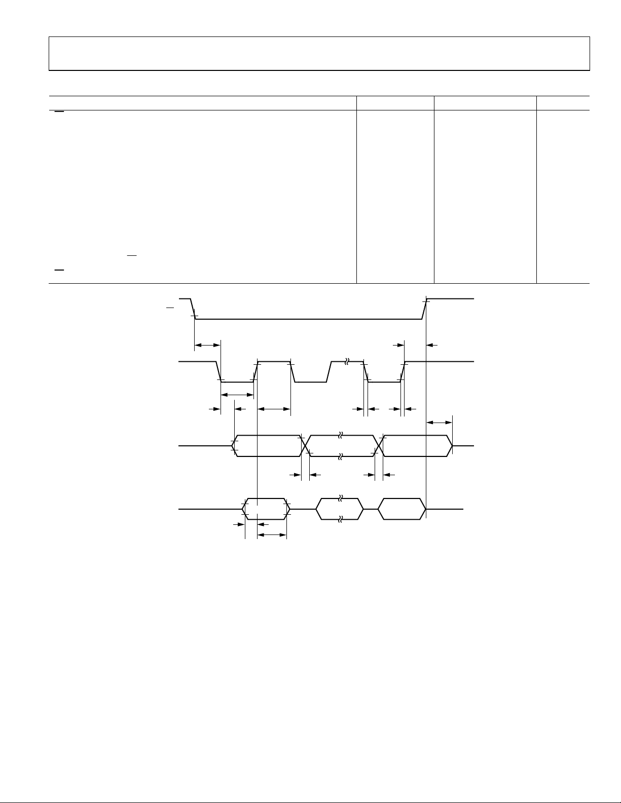
Table 3. SPI Interface Timing Parameters
Parameter Symbol Min Max Unit
t
to SCLK Edge
SS
SCLK Period 400 ns
SCLK Low Pulse Width tSL 175 ns
SCLK High Pulse Width tSH 175 ns
Data Output Valid After SCLK Edge t
Data Input Setup Time Before SCLK Edge t
Data Input Hold Time After SCLK Edge t
Data Output Fall Time tDF 20 ns
Data Output Rise Time tDR 20 ns
SCLK Rise Time tSR 20 ns
SCLK Fall Time tSF 20 ns
MISO Disable After SS Rising Edge
High After SCLK Edge
SS
SS
t
SS
50 ns
SS
100 ns
DAV
100 ns
DSU
5 ns
DHD
t
200 ns
DIS
t
0 ns
SFS
t
SFS
SCLK
MISO
MOSI
t
DAV
t
DSU
t
SL
t
SH
MSB LSB
MSB IN
t
DHD
INTERMEDIATE BITS
t
DF
INTERMEDIATE BITS
Figure 3. SPI Interface Timing
t
DR
LSB IN
t
SR
t
DIS
08510-003
t
SF
Rev. 0 | Page 9 of 92
ADE7878
K
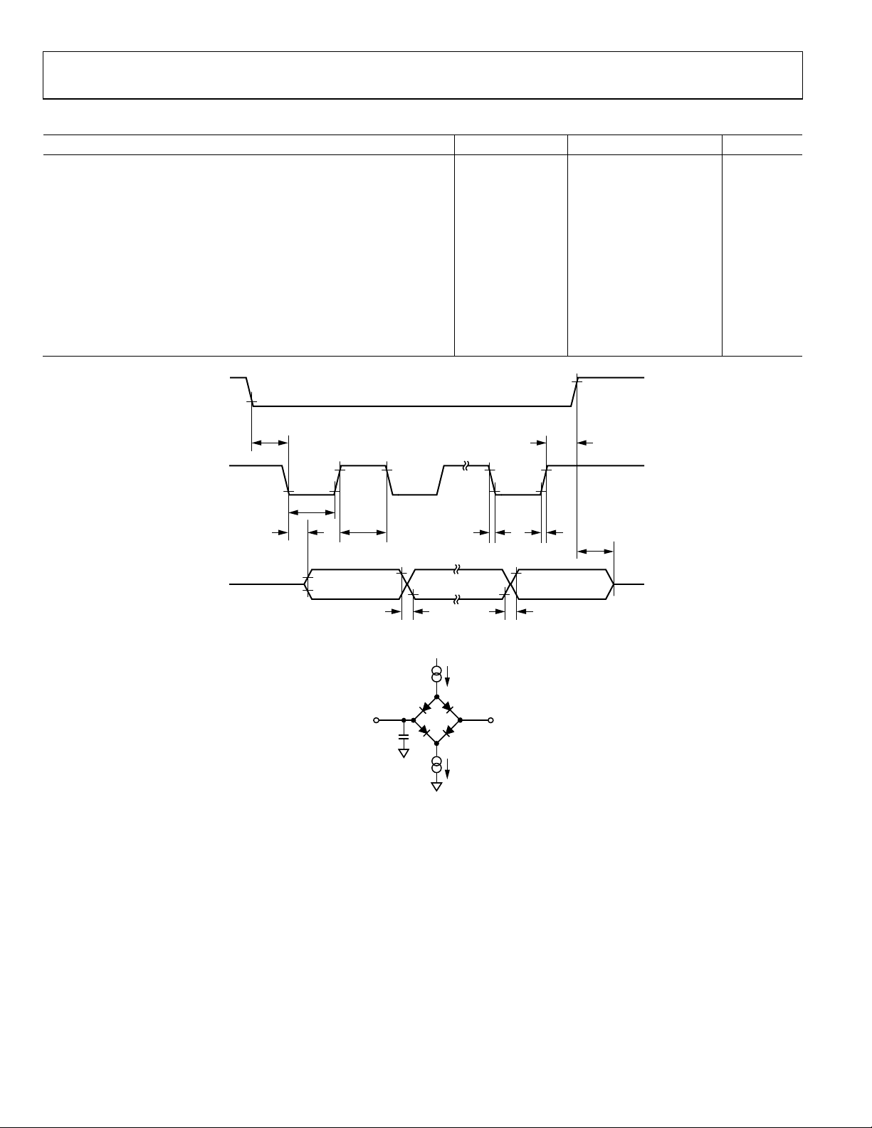
Table 4. HSDC Interface Timing Parameter
Parameter Symbol Min Max Unit
HSA to SCLK Edge t
HSCLK Period 125 ns
HSCLK Low Pulse Width tSL 50 ns
HSCLK High Pulse Width tSH 50 ns
Data Output Valid After HSCLK Edge t
Data Output Fall Time tDF 20 ns
Data Output Rise Time tDR 20 ns
HSCLK Rise Time tSR 10 ns
HSCLK Fall Time tSF 10 ns
HSD Disable After HSA Rising Edge t
HSA High After HSCLK Edge t
HSA
t
SS
HSCL
t
SL
t
t
DAV
SH
0 ns
SS
40 ns
DAV
5 ns
DIS
0 ns
SFS
t
SFS
t
SF
t
SR
t
DIS
HSD
MSB LSBINTERMEDIATE BITS
t
DF
t
DR
08510-004
Figure 4. HSDC Interface Timing
TO OUTPUT
PIN
C
50pF
2mA I
L
800µA I
OL
1.6V
OH
08510-005
Figure 5. Load Circuit for Timing Specifications
Rev. 0 | Page 10 of 92
ADE7878
ABSOLUTE MAXIMUM RATINGS
TA = 25°C, unless otherwise noted.
Table 5. Absolute Maximum Ratings
Parameter Rating
VDD to AGND −0.3 V to +3.7 V
VDD to DGND −0.3 V to +3.7 V
Analog Input Voltage to AGND, IAP, IAN,
I BP, I B N, IC P, I CN , VA P, V B P, V CP, VN
Analog Input Voltage to INP and INN −2 V to +2 V
Reference Input Voltage to AGND −0.3 V to VDD + 0.3 V
Digital Input Voltage to DGND −0.3 V to VDD + 0.3 V
Digital Output Voltage to DGND −0.3 V to VDD + 0.3 V
Operating Temperature
Industrial Range −40°C to +85°C
Storage Temperature Range −65°C to +150°C
Junction Temperature 150°C
Lead Temperature Range
(Soldering, 10 sec)
−2 V to +2 V
300°C
Stresses above those listed under Absolute Maximum Ratings
may cause permanent damage to the device. This is a stress
rating only; functional operation of the device at these or any
other conditions above those listed in the operational sections
of this specification is not implied. Exposure to absolute
maximum rating conditions for extended periods may affect
device reliability.
THERMAL RESISTANCE
θJA is specified equal to 29.3°C/W; θJC is specified equal to
1.8°C/W.
Table 6. Thermal Resistance
Package Type θJA θ
40-Lead LFCSP 29.3 1.8 °C/W
Unit
JC
ESD CAUTION
Rev. 0 | Page 11 of 92

ADE7878
PIN CONFIGURATION AND FUNCTION DESCRIPTIONS
/HSD
I/SDA
CF1
CF2
CF3/HSCLK
SCLK/SCL
MISO
MOS
SS/HSA
NC
37
38
39
40
PIN 1
1NC
INDICATOR
2PM0
3PM1
4
RESET
5DVDD
6DG ND
7IAP
8IAN
9IBP
10NC
NOTES
1. NC = NO CONNECT.
2. THE EXPOSED PAD SHOULD BE CONNECTED
TO AGND.
ADE7878
TOP VIEW
(Not to Scale)
11
12
13
14
NC
ICP
IBN
ICN
Figure 6. Pin Configuration
Table 7. Pin Function Descriptions
Pin No. Mnemonic Description
1, 10, 11, 20,
NC No Connect. These pins are not connected internally.
21, 30, 31, 40
2 PM0 Power Mode Pin 0. This pin, combined with PM1, defines the power mode of the ADE7878, as
described in Table 8.
3 PM1 Power Mode Pin 1. This pin defines the power mode of the ADE7878 when combined with PM0, as
described in Table 8.
4
RESET
Reset Input, Active Low. In PSM0 mode, this pin should stay low for at least 10 µs to trigger a
hardware reset.
5 DVDD This pin provides access to the on-chip 2.5 V digital LDO. Do not connect any external active
circuitry to this pin. Decouple this pin with a 4.7 µF capacitor in parallel with a ceramic 220 nF
capacitor.
6 DGND Ground Reference. This pin provides the ground reference for the digital circuitry.
7, 8 IAP, IAN Analog Inputs for Current Channel A. This channel is used with the current transducers and is
referenced in this document as Current Channel A. These inputs are fully differential voltage inputs
with a maximum differential level of ±0.5 V. This channel also has an internal PGA, equal to the ones
on Channel B and Channel C.
9, 12 IBP, IBN Analog Inputs for Current Channel B. This channel is used with the current transducers and is
referenced in this document as Current Channel B. These inputs are fully differential voltage inputs
with a maximum differential level of ±0.5 V. This channel also has an internal PGA equal to the ones
on Channel C and Channel A.
13, 14 ICP, ICN Analog Inputs for Current Channel C. This channel is used with the current transducers and is
referenced in this document as Current Channel C. These inputs are fully differential voltage inputs
with a maximum differential level of ±0.5 V. This channel also has an internal PGA equal to the ones
on Channel A and Channel B.
15, 16 INP, INN Analog Inputs for Neutral Current Channel N. This channel is used with the current transducers and
is referenced in this document as Current Channel N. These inputs are fully differential voltage
inputs with a maximum differential level of ±0.5 V. This channel also has an internal PGA, different
from the ones found on the A, B, and C channels.
17 REF
This pin provides access to the on-chip voltage reference. The on-chip reference has a nominal
IN/OUT
value of 1.2 V. An external reference source with 1.2 V ± 8% can also be connected at this pin. In
either case, decouple this pin to AGND with a 4.7 µF capacitor in parallel with a ceramic 100 nF
capacitor. After reset, the on-chip reference is enabled.
NC
IRQ1
32
31
33
34
35
36
30 NC
29
IRQ0
28 CL KOUT
27 CL KIN
26 VDD
25 AG ND
24 AVDD
23 VAP
22 VBP
21 NC
16
18
19
15
20
17
C
VN
N
INP
INN
VCP
IN/OUT
REF
08510-106
Rev. 0 | Page 12 of 92

ADE7878
Pin No. Mnemonic Description
18, 19, 22, 23 VN, VCP, VBP, VAP Analog Inputs for the Voltage Channel. This channel is used with the voltage transducer and is
referenced as the voltage channel in this document. These inputs are single-ended voltage inputs
with a maximum signal level of ±0.5 V with respect to VN for specified operation. This channel also
has an internal PGA.
24 AVDD This pin provides access to the on-chip 2.5 V analog low dropout regulator (LDO). Do not connect
external active circuitry to this pin. Decouple this pin with a 4.7 µF capacitor in parallel with a
ceramic 220 nF capacitor.
25 AGND Ground Reference. This pin provides the ground reference for the analog circuitry. Tie this pin to the
analog ground plane or to the quietest ground reference in the system. Use this quiet ground
reference for all analog circuitry, for example, antialiasing filters, current, and voltage transducers.
26 VDD Suppy Voltage. This pin provides the supply voltage. In PSM0 (normal power mode), maintain the
supply voltage at 3.3 V ± 10% for specified operation. In PSM1 (reduced power mode), PSM2 (low
power mode), and PSM3 (sleep mode), when the ADE7878 is supplied from a battery, maintain the
supply voltage between 2.4 V and 3.7 V. Decouple this pin to DGND with a 10 µF capacitor in
parallel with a ceramic 100 nF capacitor.
27 CLKIN Master Clock. An external clock can be provided at this logic input. Alternatively, a parallel resonant
AT-cut crystal can be connected across CLKIN and CLKOUT to provide a clock source for the
ADE7878. The clock frequency for specified operation is 16.384 MHz. Use ceramic load capacitors of
a few tens of picofarad with the gate oscillator circuit. Refer to the crystal manufacturer’s data sheet
for load capacitance requirements.
28 CLKOUT A crystal can be connected across this pin and CLKIN (as previously described with Pin 27 in this
table) to provide a clock source for the ADE7878. The CLKOUT pin can drive one CMOS load when
either an external clock is supplied at CLKIN or a crystal is being used.
29, 32
33, 34, 35 CF1, CF2,
36 SCLK/SCL Serial Clock Input for SPI Port/Serial Clock Input for I2C Port. All serial data transfers are synchronized
37 MISO/HSD Data Out for SPI Port/Data Out for HSDC Port.
38 MOSI/SDA Data In for SPI Port/Data Out for I2C Port.
39
EP Exposed Pad Connect the exposed pad to AGND.
,
IRQ1
IRQ0
CF3/HSCLK
/HSA
SS
Interrupt Request Outputs. These are active low logic outputs. See the Interrupts section for a
detailed presentation of the events that may trigger interrupts.
Calibration Frequency (CF) Logic Outputs. These outputs provide power information based on the
CF1SEL, CF2SEL, and CF3SEL bits in the CFMODE register. These outputs are used for operational and
calibration purposes. The full-scale output frequency can be scaled by writing to the CF1DEN,
CF2DEN, and CF3DEN registers, respectively (see the Energy-to-Frequency Conversion section). CF3
is multiplexed with the serial clock output of the HSDC port.
to this clock (see the Serial Interfaces section). This pin has a Schmidt trigger input for use with a
clock source that has a slow edge transition time, for example, opto-isolator outputs.
Slave Select for SPI Port/HSDC Port Active.
Rev. 0 | Page 13 of 92
ADE7878
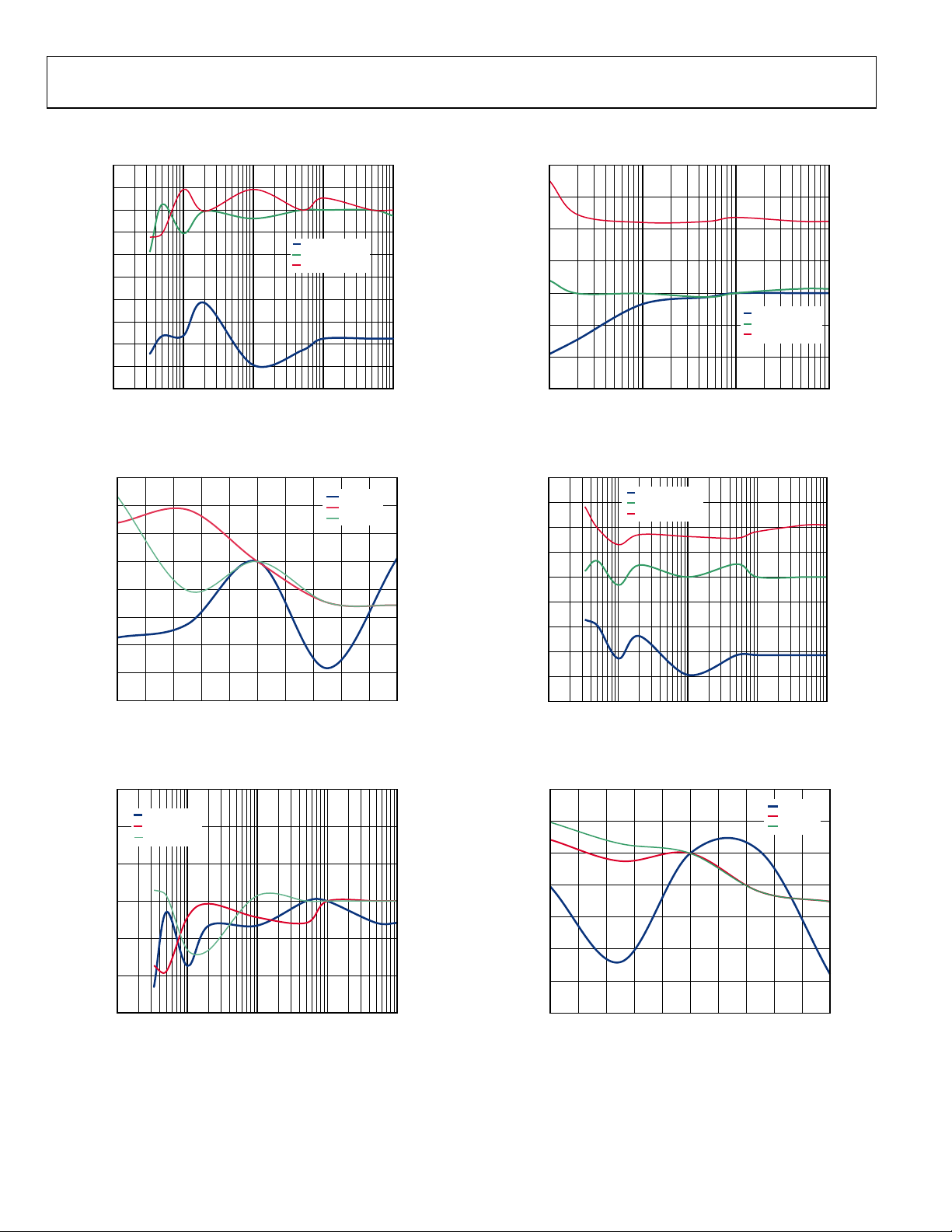
TYPICAL PERFORMANCE CHARACTERISTICS
0.10
0.05
0
–0.05
–0.10
–0.15
–0.20
ERROR (%)
–0.25
–0.30
–0.35
–0.40
0.01 0.1 1 10
FULL-SCAL E CURRENT (%)
Figure 7. Total Active Energy Error As Percentage of Reading (Gain = +1,
pF = 1) over Temperature with Internal Reference and Integrator Off
0.15
0.10
0.05
0
–0.05
ERROR (%)
–0.10
–0.15
–0.20
–0.25
45 47 49 51 53 55 57 59 61 63 65
LINE FREQUENCY (Hz)
Figure 8. Total Active Energy Error As Percentage of Reading (Gain = +1,
pF = 1) over Frequency with Internal Reference and Integrator Off
0.15
VDD = 2.97V
V
0.10
0.05
0
ERROR (%)
–0.05
= 3.30V
DD
VDD = 3.63V
–40°C, pf = 1.0
+25°C, pf = 1.0
+85°C, pf = 1.0
pf = 1
pf = +0.5
pf = –0.5
100
08510-301
08510-305
0.80
0.60
0.40
0.20
0
ERROR (%)
–0.20
–0.40
–0.60
0.1 1 10 100
FULL-SCAL E CURRENT (%)
–40°C, pf = 1.0
+25°C, pf = 1.0
+85°C, pf = 1.0
08510-308
Figure 10. Total Active Energy Error As Percentage of Reading (Gain = +16)
over Temperature with Internal Reference and Integrator On
0.40
0.30
0.20
0.10
0
–0.10
ERROR (%)
–0.20
–0.30
–0.40
–0.50
0.01 0.1 1 10 100
–40°C, pf = 0
+25°C, pf = 0
+85°C, pf = 0
FULL-SCAL E CURRENT (%)
08510-311
Figure 11. Total Reactive Energy Error As Percentage of Reading (Gain = +1,
pF = 0) over Temperature with Internal Reference and Integrator Off
0.10
pf = 0
pf = +0.5
pf = –0.5
ERROR (%)
0.05
0
–0.05
–0.10
–0.15
–0.10
–0.15
0.01 0.1 1 10 100
FULL-SCAL E CURRENT (%)
Figure 9. Total Active Energy Error As Percentage of Reading (Gain = +1,
pF = 1) over Power Supply with Internal Reference and Integrator Off
Rev. 0 | Page 14 of 92
–0.20
–0.25
45 47 49 51 53 55 57 59 61 63 65
08510-306
LINE FREQ UENCY (Hz)
08510-315
Figure 12. Total Reactive Energy Error As Percentage of Reading (Gain = +1)
over Frequency with Internal Reference and Integrator Off
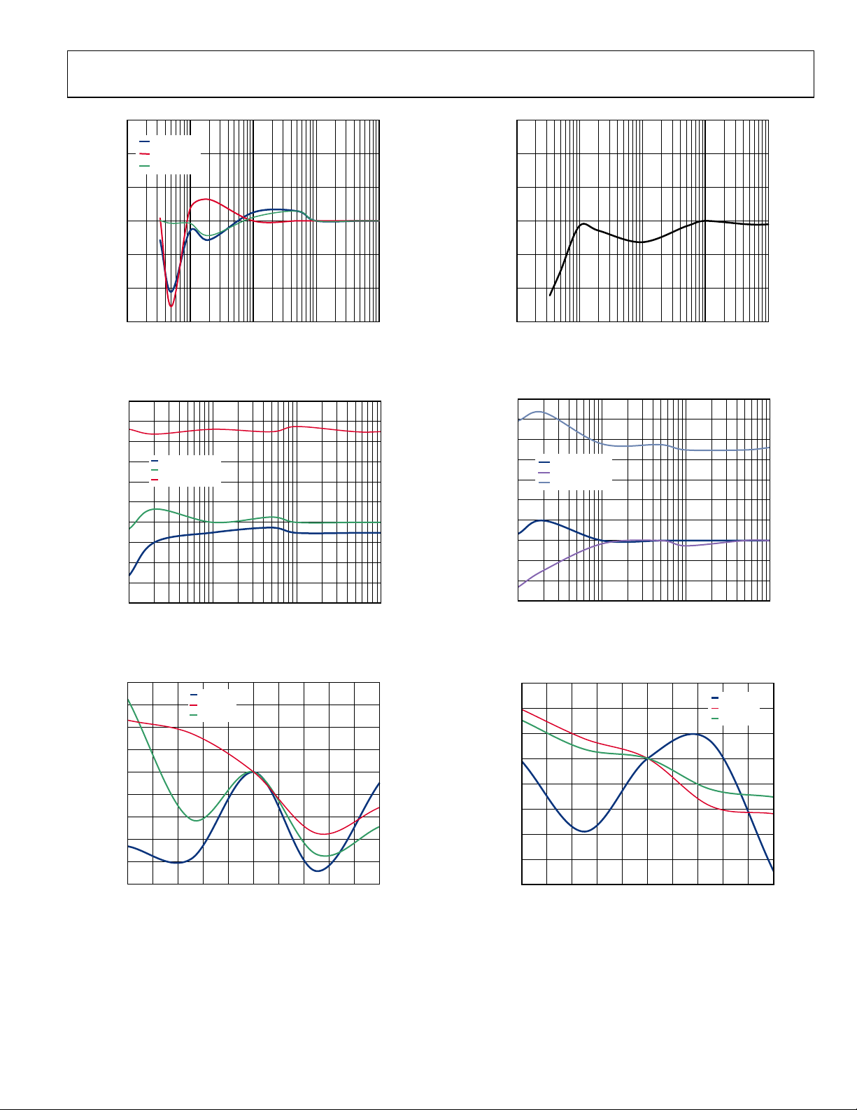
ADE7878
0.30
0.20
0.10
VDD = 2.97V
VDD = 3.30V
VDD = 3.63V
0.15
0.10
0.05
0
ERROR (%)
–0.10
–0.20
–0.30
0.01 0. 1 1 10 100
FULL-SCAL E CURRENT (%)
08510-316
Figure 13. Total Reactive Energy Error As Percentage of Reading (Gain = +1)
over Power Supply with Internal Reference and Integrator Off
0.60
0.50
0.40
–40°C, pf = 1.0
+25°C, pf = 1.0
+85°C, pf = 1.0
0.1 1 10 100
FULL-SCAL E CURRENT (%)
08510-318
ERROR (%)
0.30
0.20
0.10
0
–0.10
–0.20
–0.30
–0.40
Figure 14. Total Reactive Energy Error As Percentage of Reading (Gain = +16)
over Temperature with Internal Reference and Integrator On
0.20
0.15
0.10
0.05
0
–0.05
ERROR (%)
–0.10
–0.15
–0.20
–0.25
45 47 49 51 53 55 57 59 61 63 65
pf = 1.0
pf = +0.5
pf = –0.5
LINE FREQUENCY (Hz)
08510-335
Figure 15. Fundamental Active Energy Error As Percentage of Reading
(Gain = +1) over Frequency with Internal Reference and Integrator Off
0
ERROR (%)
–0.05
–0.10
–0.15
0.01 0. 10 1.00 10.00 100. 00
FULL-SCAL E CURRENT (%)
08510-337
Figure 16. CF Fundamental Active Energy Error As a Percentage of Reading
(Gain = +1) with Internal Reference and Integrator Off
0.70
0.60
0.50
0.40
0.30
0.20
0.10
ERROR (%)
0
–0.10
–0.20
–0.30
0.10 1. 00 10.00 100.00
+25°C, pf = 1.0
–40°C, pf = 1.0
+85°C, pf = 1.0
FULL-SCAL E CURRENT (%)
Figure 17. Fundamental Active Energy Error As Percentage of Reading
(Gain = +16) over Temperature with Internal Reference and Integrator On
0.15
0.10
0.05
0
–0.05
ERROR (%)
–0.10
–0.15
–0.20
–0.25
45 47 49 51 53 55 57 59 61 63 65
LINE FREQUENCY (Hz)
pf = 1.0
pf = +0.5
pf = –0.5
08510-345
Figure 18. Fundamental Reactive Energy Error As Percentage of Reading
(Gain = +1) over Frequency with Internal Reference and Integrator Off
08510-338
Rev. 0 | Page 15 of 92
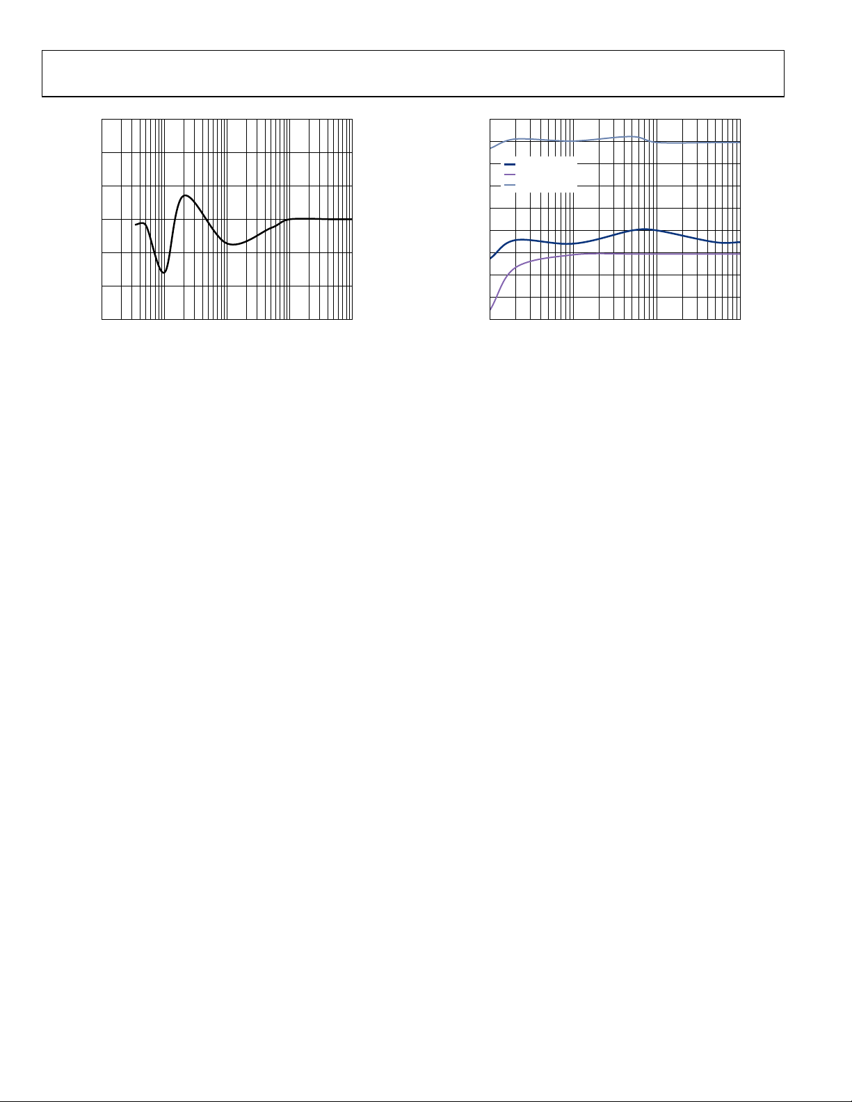
ADE7878
0.15
0.10
0.05
0
ERROR (%)
–0.05
–0.10
ERROR (%)
0.50
0.40
0.30
0.20
0.10
–0.10
–0.20
–0.30
0
+25°C, pf = 1.0
–40°C, pf = 1.0
+85°C, pf = 1.0
–0.15
0.01 0.10 1.00 10.00 100. 00
FULL-SCAL E CURRENT (%)
08510-347
Figure 19. CF Fundamental Reactive Energy Error As a Percentage of Reading
(Gain = +1) with Internal Reference and Integrator Off
–0.40
0.10 1.00 10.00 100.00
FULL-SCAL E CURRENT (%)
Figure 20. Fundamental Reactive Energy Error As Percentage of Reading
(Gain = +16) over Temperature with Internal Reference and Integrator On
08510-348
Rev. 0 | Page 16 of 92

ADE7878
V
TEST CIRCUIT
1kΩ
1kΩ
1kΩ
1kΩ
10kΩ
1.8nF
1.8nF
1.8nF
1.8nF
3.3V
SAME AS
IAP, IAN
SAME AS
IAP, IAN
SAME AS
VCP
SAME AS
VCP
+ +
2
3
4
7
8
9
12
13
14
18
19
22
23
0.22µF
PM0
PM1
RESET
IAP
IAN
IBP
IBN
ICP
ICN
VN
VCP
VBP
VAP
4.7µF
1µF
Figure 21. Test Circuit
3.3
26
24
VDD
AVD D
ADE7858
AGND
DGND
25
6
10µF
5
DVDD
SS/HSA
MOSI/SDA
MISO/HSD
SCLK/SCL
CF3/HSCLK
CF2
CF1
IRQ1
IRQ0
REF
IN/OUT
CLKOUT
CLKIN
PAD
39
38
37
36
35
34
33
32
29
17
28
27
0.1µF
SAME AS
CF2
SAME AS
IRQ0_N
20pF
16.384MHz
20pF
10kΩ
4.7µF
10kΩ
3.3V
3.3V
1.5kΩ
+
0.1µF
08510-099
Rev. 0 | Page 17 of 92

ADE7878
y
y
d
y
+
−
M
M
TERMINOLOGY
Measurement Error
The error associated with the energy measurement made by the
ADE7878 is defined by
Measurement Error =
Registere
Energ
EnergyTrue
Phase Error Between Channels
The high-pass filter (HPF) and digital integrator introduce a
slight phase mismatch between the current and the voltage
channel. The all digital design ensures that the phase matching
between the current channels and voltage channels in all three
phases is within ±0.1° over a range of 45 Hz to 65 Hz and ±0.2°
over a range of 40 Hz to 1 kHz. This internal phase mismatch
can be combined with the external phase error (from current
sensor or component tolerance) and calibrated with the phase
calibration registers.
Power Supply Rejection (PSR)
This quantifies the ADE7878 measurement error as a percentage of reading when the power supplies are varied. For the ac
PSR measurement, a reading at nominal supplies (3.3 V) is
taken. A second reading is obtained with the same input signal
levels when an ac signal (120 mV rms at 100 Hz) is introduced
onto the supplies. Any error introduced by this ac signal is
expressed as a percentage of reading—see the Measurement
Error definition.
For the dc PSR measurement, a reading at nominal supplies
(3.3 V) is taken. A second reading is obtained with the same
input signal levels when the power supplies are varied ±10%.
Any error introduced is expressed as a percentage of the
reading.
7878×−
TrueADEb
Energ
%100
(1)
ADC Offset Error
This refers to the dc offset associated with the analog inputs to
the ADCs. It means that with the analog inputs connected to
AGND, the ADCs still see a dc analog input signal. The magnitude of the offset depends on the gain and input range selection
(see the Typical Perfor m a n c e Characte r istics section). However,
a HPF removes the offset from the current and voltage channels
and the power calculation remains unaffected by this offset.
Gain Error
The gain error in the ADCs of the ADE7878 is defined as the
difference between the measured ADC output code (minus the
offset) and the ideal output code (see the Current Channel ADC
section and the Volt age C han nel AD C section). The difference
is expressed as a percentage of the ideal code.
CF Jitter
The period of pulses at one of the CF1, CF2, or CF3 pins is
continuously measured. The maximum, minimum, and average
values of four consecutive pulses are computed as follows:
Maximum = max(Period
Minimum = min(Period
Average =
, Period1, Period2, Period3)
0
, Period1, Period2, Period3)
0
PeriodPeriodPeriodPeriod ++
4
3210
The CF jitter is then computed as
CF
JITTER
=
aximum
Average
inimum
%100×
(2)
Rev. 0 | Page 18 of 92

ADE7878
POWER MANAGEMENT
The ADE7878 has four modes of operation, determined by the
state of the PM0 and PM1 pins (see Table 8). These pins provide
complete control of the ADE7878 operation and can easily be
connected to an external microprocessor I/O. The PM0 and
PM1 pins have internal pull-up resistors. Tab le 1 0 and Tab l e 11
list actions that are recommended before and after setting a new
power mode.
Table 8. ADE7878 Power Supply Modes
Power Supply Modes PM1 PM0
PSM0, Normal Power Mode 0 1
PSM1, Reduced Power Mode 0 0
PSM2, Low Power Mode 1 0
PSM3, Sleep Mode 1 1
PSM0—NORMAL POWER MODE
In PSM0 mode, the ADE7878 is fully functional. The PM0 pin
is set to high and the PM1 pin is set to low for the ADE7878 to
enter this mode. If the ADE7878 is in one of PSM1, PSM2, or
PSM3 modes and is switched into PSM0 mode, then all control
registers take the default values with the exception of the threshold
register, LPOILVL[7:0], which is used in PSM2 mode, and the
CONFIG2[7:0] register, both of which maintain their values.
The ADE7878 signals the end of the transition period by triggering
IRQ1
the
the STATUS1[31:0] register to 1. This bit is 0 during the transition
period and becomes 1 when the transition is finished. The status
bit is cleared and the
STATUS1[31:0] register with the corresponding bit set to 1.
Bit 15 (RSTDONE) in the interrupt mask register does not have
any functionality attached even if the
Bit 15 (RSTDONE) in the STATUS1[31:0] register is set to 1.
This makes the RSTDONE interrupt unmaskable.
interrupt pin low and setting Bit 15 (RSTDONE) in
IRQ1
pin is set back to high by writing
IRQ1
pin goes low when
PSM1—REDUCED POWER MODE
In this mode, the ADE7878 measures the mean absolute values
(mav) of the 3-phase currents and stores the results in the
AIMAV[19:0], BIMAV[19:0], and CIMAV[19:0] 20-bit
registers. This mode is useful in missing neutral cases in which
the voltage supply of the ADE7878 is provided by an external
battery. The serial ports, I
and the active port can be used to read the AIMAV, BIMAV, and
CIMAV registers. It is not recommended to read any of the other
registers because their values are not guaranteed in this mode.
Similarly, a write operation is not taken into account by the
ADE7878 in this mode. In summary, in this mode, it is not
recommended to access any register other than AIMAV,
BIMAV, and CIMAV. The circuit that measures these estimates
of rms values is also active during PSM0; therefore, its calibration
can be completed in either PSM0 mode or in PSM1 mode. Note
2
C or SPI, are enabled in this mode
Rev. 0 | Page 19 of 92
that the ADE7878 does not provide any register to store or
process the corrections resulting from the calibration process.
The external microprocessor should store the gain values in
connection with these measurements and use them during
PSM1 (see the Current Mean Absolute Value Calculation
section for more details on the xIMAV registers).
The 20-bit mean absolute value measurements done in PSM1,
although available also in PSM0, are different from the rms
measurements of phase currents and voltages executed only in
PSM0 and stored in xIRMS and xVRMS 24-bit registers. See the
Current Mean Absolute Value Calculation section for details.
If the ADE7878 is set in PSM1 mode while still in PSM0, the
ADE7878 immediately begins the mean absolute value calculations without any delay. The xIMAV registers can be accessed at
any time; however, if the ADE7878 is set in PSM1 mode while
still in PSM2 or PSM3 modes, the ADE7878 signals the start of
IRQ1
the mean absolute value computations by triggering the
pin low. The xIMAV registers can be accessed only after this
moment.
PSM2—LOW POWER MODE
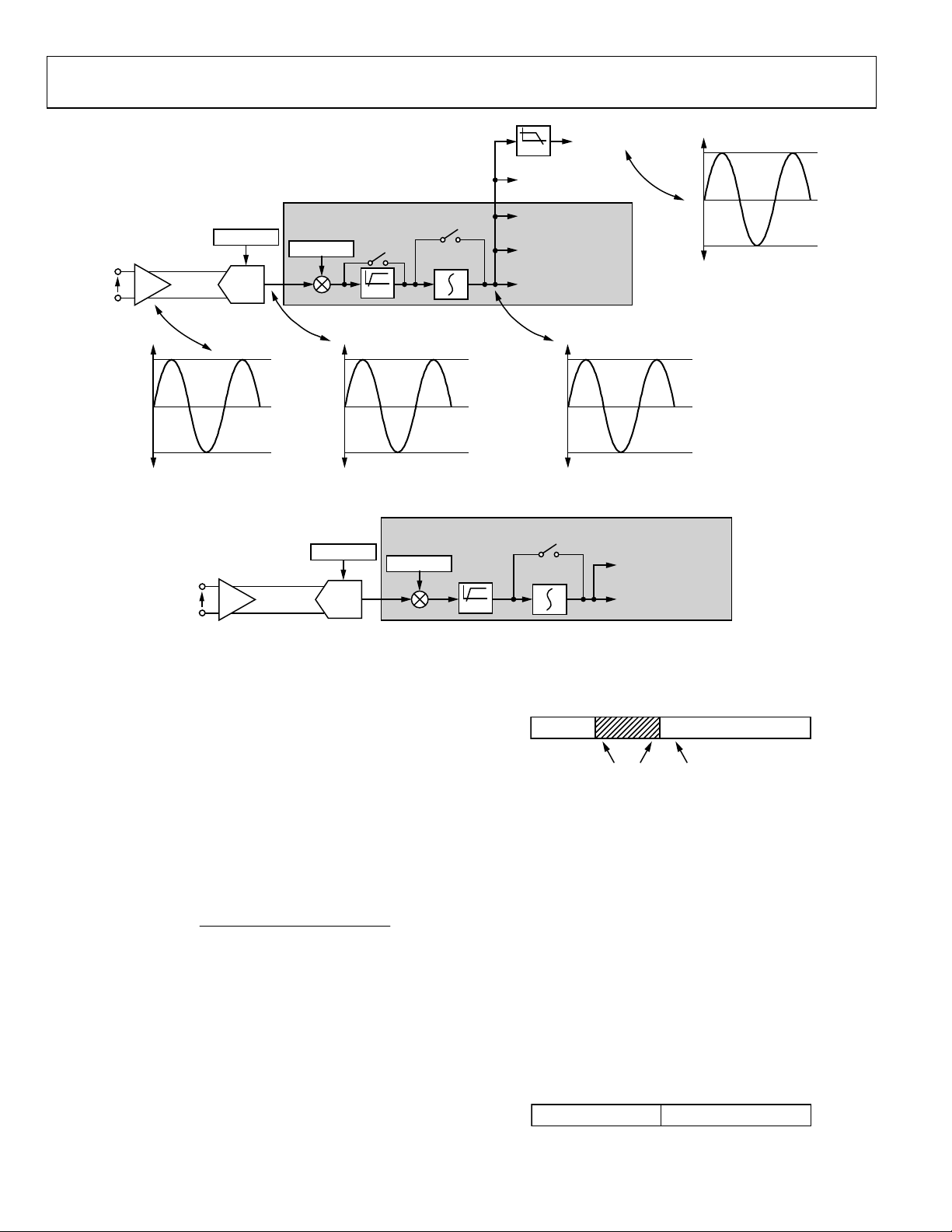
In this mode, the ADE7878 compares all phase currents against
a threshold for a period of 0.02 × (LPLINE + 1) seconds,
independent of the line frequency. LPLINE are Bits[7:3] of the
LPOILVL[7:0] register (see Tab l e 9).
Table 9. LPOILVL Register
Bit Mnemonic Default Description
[2:0] LPOIL 111 Threshold is put at a value
corresponding to full scale
multiplied by LPOIL/8.
[7:3] LPLINE 00000 The measurement period is
(LPLINE + 1)/50 sec.
The threshold is derived from Bits[2:0] (LPOIL) of the
LPOILVL[7:0] register as LPOIL/8 of full scale. Every time
one phase current becomes greater than the threshold, a
counter is incremented. If every phase counter remains below
LPLINE + 1 at the end of the measurement period, then the
IRQ0
pin is triggered low. If a single phase counter becomes
greater or equal to LPLINE + 1 at the end of the measurement
period, the
the ADE7878 behaves in PSM2 mode when LPLINE = 2 and
LPOIL = 3. The test period is three 50 Hz cycles (60 ms), and
the Phase A current rises above the LPOIL threshold three times.
At the end of the test period, the
The I
PSM2 mode reduces the power consumption required to monitor the currents when there is no voltage input and the voltage
supply of the ADE7878 is provided by an external battery. If the
IRQ1
pin is triggered low. illustrates how
2
C or SPI port is not functional during this mode. The
Figure 22
IRQ1
pin is triggered low.
ADE7878
T
0IRQ pin is triggered low at the end of a measurement period,
this signifies all phase currents stayed below threshold and,
therefore, there is no current flowing through the system. At
this point, the external microprocessor should set the ADE7878
in Sleep Mode PSM3. If the
end of the measurement period, this signifies that at least one
current input is above the defined threshold and current is
flowing through the system, although no voltage is present at
the ADE7878 pins. This situation is often called missing neutral
and is considered a tampering situation, at which point the
external microprocessor should set the ADE7878 in PSM1
mode, measure mean absolute values of phase currents, and
integrate the energy based on their values and the nominal
voltage.
It is recommended to use the ADE7878 in PSM2 mode when
Bits[2:0] (PGA1) of the Gain[15:0] register are equal to 1 or 2.
These bits represent the gain in the current channel datapath. It
is not recommended to use the ADE7878 in PSM2 mode when
the PGA1 bits are equal to 4, 8, or 16.
IA CURREN
PHASE
COUNTER = 1
IRQ 1
Figure 22. PSM2 Mode Triggering
1IRQ pin is triggered low at the
LPLINE = 2
PHASE
COUNTER = 2
IRQ1
PHASE
COUNTER = 3
Pin for LPLINE = 2, 50 Hz Systems
LPOIL
THRESHOLD
PSM3—SLEEP MODE
In this mode, the ADE7878 has most of the internal circuits
turned off and the current consumption is at its lowest level.
2
C, HSDC, and SPI ports are not functional during this
The I
mode, and the
RESET
, SCLK/SCL, MOSI/SDA, and SS/HSA
pins should be set high.
POWER-UP PROCEDURE
The ADE7878 contains an on-chip power supply monitor that
supervises the power supply (VDD). At power-up, until VDD
reaches 2 V ± 10%, the chip is in an inactive state. As VDD
crosses this threshold, the power supply monitor keeps the chip
in this inactive state for an additional 26 ms, allowing VDD to
achieve 3.3 V − 10%, the minimum recommended supply
voltage. Because the PM0 and PM1 pins have internal pull-up
resistors and the external microprocessor keeps them high, the
ADE7878 always powers-up in sleep mode (PSM3). Then, an
external circuit (that is, a microprocessor) sets the PM1 pin to a
low level, allowing the ADE7878 to enter normal mode (PSM0).
The passage from PSM3 mode, in which most of the internal
circuitry is turned off, to PSM0 mode, in which all functionality
is enabled, is accomplished in less than 40 ms (see Figure 23 for
details).
2
When the ADE7878 enters PSM0 mode, the I
active serial port. If the SPI port is used, then the
must be toggled three times high to low. This action selects the
SPI port for further use. If I
2
C is the active serial port, Bit 1
(I2C_LOCK) of CONFIG2[7:0] must be set to 1 to lock it in.
From this moment, the ADE7878 ignores spurious toggling of
SS
the
/HSA pin, and an eventual switch to use the SPI port is no
longer possible. Likewise, if SPI is the active serial port, any write
to the CONFIG2[7:0] register locks the port, at which time a
2
08510-008
switch to use the I
C port is no longer possible.
C port is the
SS
/HSA pin
3.3V – 10%
2.0V ± 10%
0V
40ms26ms
ADE7878
POWERED UP
POR TIMER
TURNED ON
ADE7878
ENTER PSM3
Figure 23. Power-Up Procedure
Rev. 0 | Page 20 of 92
MICROPROCESSOR
SETS ADE7878
IN PSM0
RSTDONE
INTERRUPT
TRIGGERED
ADE7878
PSM0 READY
MICROPROCESSOR
MAKES THE
CHOICE BETWE EN
2
C AND SPI
I
08510-009

ADE7878
Only a power-down or setting the
ADE7878 to use the I
2
C port. Once locked, the serial port choice is
RESET
pin low can reset the
maintained when the ADE7878 changes PSMx power modes.
Immediately after entering PSM0, theADE7878 sets all registers to their default values, including CONFIG2[7:0] and
LPOILVL[7:0].
The ADE7878 signals the end of the transition period by
triggering the
IRQ1
interrupt pin low and setting Bit 15
(RSTDONE) in the STATUS1[31:0] register to 1. This bit is
0 during the transition period and becomes 1 when the transition ends. The status bit is cleared and the
IRQ1
pin is returned
high by writing the STATUS1[31:0] register with the corresponding
bit set to 1. Because the RSTDONE is an unmaskable interrupt,
Bit 15 (RSTDONE) in the STATUS1[31:0] register must be
cancelled for the
to wait until the
IRQ1
pin to return high. It is recommended
IRQ1
pin goes low before accessing the
STATUS1[31:0] register to test the state of the RSTDONE bit.
At this point, as a good programming practice, it is also
recommended to cancel all other status flags in the
STATUS1[31:0] and STATUS0[31:0] registers by writing
the corresponding bits with 1.
Initially, the DSP is in idle mode, which means it does not
execute any instruction. This is the moment to initialize all
ADE7878 registers and then write 0x0001 into the Run[15:0]
register to start the DSP (see the Digital Signal Processor
section for details on the Run[15:0] register).
If the supply voltage, VDD, drops lower than 2 V ± 10%, the
ADE7878 enters an inactive state, which means that no
measurements and computations are executed.
HARDWARE RESET
The ADE7878 has a
mode and the
the hardware reset state. The ADE7878 must be in PSM0 mode
for a hardware reset to be considered. Setting the
low while the ADE7878 is in PSM1, PSM2, and PSM3 modes
does not have any effect.
If the ADE7878 is in PSM0 mode and the
from high to low and then back to high after at least 10 µs, all the
registers are set to their default values, including CONFIG2[7:0]
and LPOILVL[7:0]. The ADE7878 signals the end of the transi-
RESET
pin. If the ADE7878 is in PSM0
RESET
pin is set low, then the ADE7878 enters
RESET
RESET
pin
pin is toggled
tion period by triggering the
Bit 15 (RSTDONE) in the STATUS1[31:0] register to 1. This bit
is 0 during the transition period and becomes 1 when the transition ends. The status bit is cleared and the
returned high by writing to the STATUS1[31:0] register with
the corresponding bit set to 1.
After a hardware reset, the DSP is in idle mode, which means it
does not execute any instruction.
Because the I
2
C port is the default serial port of theADE7878, it
becomes active after a reset state. If SPI is the port used by the
external microprocessor, the procedure to enable it must be
repeated immediately after the
high (see the section for details). Serial Interfaces
At this point, it is recommended to initialize all of the ADE7878
registers and then write 0x0001 into the Run[15:0] register to
start the DSP. See the Digital Signal Processor section for details
on the Run[15:0] register.
SOFTWARE RESET FUNCTIONALITY
Bit 7 (SWRST) in the CONFIG[15:0] register manages the software reset functionality in PSM0 mode. The default value of this
bit is 0. If this bit is set to 1, then the ADE7878 enters a software
reset state. In this state, almost all internal registers are set to
their default values. In addition, the choice of what serial port,
2
C or SPI, is in use remains unchanged if the lock-in procedure
I
has been previously executed (see the Serial Interfaces for details).
The registers that maintain their values despite the SWRST bit
being set to 1 are CONFIG2[7:0] and LPOILVL[7:0]. When the
software reset ends, Bit 7 (SWRST) in CONFIG[15:0] is cleared
IRQ1
to 0, the
in the STATUS1[31:0] register is set to 1. This bit is 0 during the
transition period and becomes 1 when the transition ends. The
status bit is cleared and the
the STATUS1[31:0] register with the corresponding bit set to 1.
After a software reset ends, the DSP is in idle mode, which
means it does not execute any instruction. It is recommended
to initialize all the ADE7878 registers and then write 0x0001
into the Run[15:0] register to start the DSP (see the Digital
Signal Processor section for details on the Run[15:0] register).
Software reset functionality is not available in PSM1, PSM2, or
PSM3 mode.
interrupt pin is set low, and Bit 15 (RSTDONE)
IRQ1
interrupt pin low and setting
IRQ1
pin is
RESET
pin is toggled back to
IRQ1
pin is set back high by writing to
Rev. 0 | Page 21 of 92

ADE7878
Table 10. Power Modes and Related Characteristics
LPOILVL,
Power Mode All Registers1
PSM0
State After Hardware Reset Set to default Set to default I2C enabled All circuits are active and
State After Software Reset Set to default Unchanged Active serial port is unchanged if lock
PSM1 Not available Values set
PSM2 Not available Values set
PSM3 Not available Values set
1
Setting for all registers except the LPOILVL and CONFIG2 registers.
CONFIG2 I2C/SPI Functionality
DSP is in idle mode.
All circuits are active and
in procedure has been previously
DSP is in idle mode.
executed
Enabled Current mean absolute
during PSM0
unchanged.
values are computed and
the results are stored in
the AIMAV, BIMAV, and
CIMAV registers. The I
SPI serial port is enabled
with limited functionality.
Disabled Compares phase currents
during PSM0
unchanged
against the threshold set
in LPOILVL. Triggers
or
pins accordingly.
IRQ1
The serial ports are not
available.
Disabled Internal circuits shut down
during PSM0
unchanged
and the serial ports are
not available.
2
C or
IRQ0
Rev. 0 | Page 22 of 92

ADE7878
Table 11. Recommended Actions When Changing Power Modes
Initial
Power
Mode
PSM0
PSM1
PSM2
PSM3
Recommended Actions
Before Setting Next
Power Mode
Stop DSP by setting
Run[15:0] = 0x0000.
Disable HSDC by clearing
Bit 6 (HSDEN) to 0 in the
CONFIG[15:0] register.
Mask interrupts by setting
MASK0[31:0] = 0x0 and
MASK1[31:0] = 0x0.
Erase interrupt status flags in
the STATUS0[31:0] and
STATUS1[31:0] registers.
No action necessary.
No action necessary.
No action necessary.
Next Power Mode
PSM0 PSM1 PSM2 PSM3
Current mean absolute
values (mav) computed
immediately.
Wait until the
pin is triggered
IRQ1
accordingly.
IRQ0
or
No action
necessary.
xIMAV[19:0] registers may
be accessed immediately.
Wait until the
IRQ1
pin is
triggered low.
Poll the STATUS1[31:0]
Wait until the
pin is triggered
IRQ1
IRQ0
accordingly.
or
No action
necessary.
register until Bit 15
(RSTDONE) is set to 1.
Wait until the
IRQ1
pin is
triggered low.
Poll the STATUS1[31:0]
register until Bit 15
(RSTDONE) is set to 1.
Wait until the
IRQ1
pin
triggered low.
Current mean absolute
values are computed
beginning this moment.
No action
necessary.
xIMAV[19:0] registers may
be accessed from this
moment.
Wait until the
IRQ1
pin is
triggered low.
Poll the STATUS1[31:0]
register until Bit 15
Wait until the
IRQ1
pin is
triggered low.
Current mav circuit begins
computations at this time.
Wait until the
pin is triggered
IRQ1
accordingly.
IRQ0
or
(RSTDONE) is set to 1.
xIMAV[19:0] registers can
be accessed from this
moment.
Rev. 0 | Page 23 of 92
ADE7878
+
V
T
–
V
+
V
–
V
THEORY OF OPERATION
ANALOG INPUTS
The ADE7878 has seven analog inputs forming current and
voltage channels. The current channels consist of four pairs of
fully differential voltage inputs: IAP and IAN, IBP and IBN, ICP
and ICN, and INP and INN. These voltage input pairs have a
maximum differential signal of ±0.5 V. In addition, the
maximum signal level on analog inputs for IxP/IxN is ±0.5 V
with respect to AGND. The maximum common-mode signal
allowed on the inputs is ±25 mV. Figure 24 presents a schematic
of the current channels inputs and their relation to the
maximum common-mode voltage.
All inputs have a programmable gain amplifier (PGA) with a
possible gain selection of 1, 2, 4, 8, or 16. The gain of IA, IB, and
IC inputs is set in Bits[2:0] (PGA1) of the Gain[15:0] register.
The gain of the IN input is set in Bits[5:3] (PGA2) of the
Gain[15:0] register; thus, a different gain from the IA, IB, or IC
inputs is possible. See Tabl e 38 for details on the Gain[15:0]
register.
The voltage channel has three single-ended voltage inputs: VAP,
VBP, and VCP. These single-ended voltage inputs have a maximum
input voltage of ±0.5 V with respect to VN. In addition, the maximum signal level on analog inputs for VxP and VN is ±0.5 V
with respect to AGND. The maximum common-mode signal
allowed on the inputs is ±25 mV. Figure 26 presents a schematic
of the voltage channels inputs and their relation to the maximum
common-mode voltage.
All inputs have a programmable gain with a possible gain
selection of 1, 2, 4, 8, or 16. The setting is done using Bits[8:6]
(PGA3) in the Gain[15:0] register (see Tabl e 38 ).
Figure 25 shows how the gain selection from the Gain[15:0]
register works in both current and voltage channels.
DIFFERENTIAL INPU
V1 + V2 = 500mV MAX PEAK
V1+ V
2
500m
V
CM
500m
Figure 24. Maximum Input Level, Current Channels, Gain = 1
ANALOG-TO-DIGITAL CONVERSION
The ADE7878 has seven sigma-delta (Σ-) analog-to-digital
converters (ADCs). In PSM0 mode, all ADCs are active. In
PSM1 mode, the ADCs that measure the Phase A, Phase B, and
Phase C currents only are active. The ADCs that measure the
neutral current and the A, B, and C phase voltages are turned
COMMON MODE
= ±25mV MAX
V
CM
V
CM
V
1
V
2
IAP, IBP,
ICP OR INP
IAN, IBN,
ICN OR INN
08510-010
off. In PSM2 and PSM3 modes, the ADCs are powered down to
minimize power consumption.
For simplicity, the block diagram in Figure 27 shows a firstorder Σ- ADC. The converter is made up of the Σ- modulator
and the digital low-pass filter.
A Σ- modulator converts the input signal into a continuous
serial stream of 1s and 0s at a rate determined by the sampling
clock. In the ADE7878, the sampling clock is equal to 1.024 MHz
(CLKIN/16). The 1-bit DAC in the feedback loop is driven by
the serial data stream. The DAC output is subtracted from the
input signal. If the loop gain is high enough, the average value
of the DAC output (and therefore the bit stream) can approach
that of the input signal level. For any given input value in a
single sampling interval, the data from the 1-bit ADC is
virtually meaningless. Only when a large number of samples is
averaged is a meaningful result obtained. This averaging is
carried out in the second part of the ADC, the digital low-pass
filter. By averaging a large number of bits from the modulator,
the low-pass filter can produce 24-bit data-words that are
proportional to the input signal level.
GAIN
SELECTION
IxP, VyP
V
IN
IxN, VN
NOTES
1. x = A, B, C, N
y = A, B, C.
K × V
IN
08510-011
Figure 25. PGA in Current and Voltage Channels
DIFFERENTIAL INPUT
+ V2 = 500mV MAX PEAK
V
1
COMMON MODE
= ±25mV MAX
V
CM
V
1
V
CM
VAP, V BP
OR VCP
VN
08510-012
500m
500m
V
1
V
CM
Figure 26. Maximum Input Level, Voltage Channels, Gain = 1
V
REF
CLKIN/16
LATCHED
COMPARATOR
+
–
.....10100101.....
1-BIT DAC
Σ
-Δ ADC
DIGITAL
LOW-PASS
FILTER
24
ANALOG
LOW-PASS FILTER
R
C
INTEGRATO R
+
–
Figure 27. First-Order
08510-013
Rev. 0 | Page 24 of 92
ADE7878
A
The Σ- converter uses two techniques to achieve high resolution from what is essentially a 1-bit conversion technique. The
first is oversampling. Oversampling means that the signal is
sampled at a rate (frequency) that is many times higher than
the bandwidth of interest. For example, the sampling rate in
the ADE7878 is 1.024 MHz, and the bandwidth of interest is
40 Hz to 2 kHz. Oversampling has the effect of spreading the
quantization noise (noise due to sampling) over a wider bandwidth. With the noise spread more thinly over a wider bandwidth,
the quantization noise in the band of interest is lowered, as
shown in Figure 28. However, oversampling alone is not efficient
enough to improve the signal-to-noise ratio (SNR) in the band
of interest. For example, an oversampling ratio of 4 is required
just to increase the SNR by only 6 dB (1 bit). To keep the oversampling ratio at a reasonable level, it is possible to shape the
quantization noise so that the majority of the noise lies at the
higher frequencies. In the Σ- modulator, the noise is shaped
by the integrator, which has a high-pass-type response for the
quantization noise. This is the second technique used to achieve
high resolution. The result is that most of the noise is at the
higher frequencies where it can be removed by the digital lowpass filter. This noise shaping is shown in Figure 28.
ANTIALIAS FILTER
SIGNAL
NOISE
SIGNAL
NOISE
Figure 28. Noise Reduction Due to Oversampling and
DIGITAL FILTER
0 2 4 512
0 2 4 512
FREQUENCY (kHz)
HIGH RESOLUTION
OUTPUT FROM
DIGITAL LPF
FREQUENCY (kHz)
Noise Shaping in the Analog Modulator
(RC)
SHAPED NOISE
1024
1024
SAMPLING
FREQUENCY
08510-014
Antialiasing Filter
Figure 27 also shows an analog low-pass filter (RC) on the input
to the ADC. This filter is placed outside the ADE7878, and its
role is to prevent aliasing. Aliasing is an artifact of all sampled
systems and is illustrated in Figure 29. Aliasing means that
frequency components in the input signal to the ADC, which
are higher than half the sampling rate of the ADC, appear in the
sampled signal at a frequency below half the sampling rate.
Frequency components above half the sampling frequency (also
known as the Nyquist frequency, that is, 512 kHz) are imaged or
folded back down below 512 kHz. This happens with all ADCs
regardless of the architecture. In the example shown, only
Rev. 0 | Page 25 of 92
frequencies near the sampling frequency, that is, 1.024 MHz,
move into the band of interest for metering, that is, 40 Hz to
2 kHz. To attenuate the high frequency (near 1.024 MHz) noise
and prevent the distortion of the band of interest, a low-pass
filer (LPF) must be introduced. For conventional current
sensors, it is recommended to use one RC filter with a corner
frequency of 5 kHz for the attenuation to be sufficiently high at
the sampling frequency of 1.024 MHz. The 20 dB per decade
attenuation of this filter is usually sufficient to eliminate the
effects of aliasing for conventional current sensors. However, for a
di/dt sensor such as a Rogowski coil, the sensor has a 20 dB per
decade gain. This neutralizes the 20 dB per decade attenuation
produced by the LPF. Therefore, when using a di/dt sensor, take
care to offset the 20 dB per decade gain. One simple approach is
to cascade one additional RC filter; thus, a −40 dB per decade
attenuation is produced.
LIASING E FFECTS
0 2 4 512
IMAGE
FREQUENCIES
FREQUENCY (kHz)
Figure 29. Aliasing Effects
SAMPLING
FREQUENCY
1024
08510-015
ADC Transfer Function
All ADCs in the ADE7878 are designed to produce the same
24-bit signed output code for the same input signal level. With a
full-scale input signal of 0.5 V and an internal reference of 1.2 V,
the ADC output code is nominally 5,928,256 (0x5A7540). The
code from the ADC may vary between 0x800000 (−8,388,608)
and 0x7FFFFF (+8,388,607); this is equivalent to an input signal
level of ±0.707 V. However, for specified performance, it is
recommended not to exceed the nominal range of ±0.5 V. The
ADC performance is guaranteed only for input signals lower
than ±0.5 V.
CURRENT CHANNEL ADC
Figure 30 shows the ADC and signal processing path for
Input IA of the current channels (it is the same for IB and IC).
The ADC outputs are signed twos complement 24-bit datawords and are available at a rate of 8 kSPS (thousand samples
per second). With the specified full-scale analog input signal
of ±0.5 V, the ADC produces its maximum output code value.
Figure 30 shows a full-scale voltage signal applied to the differential inputs (IAP and IAN). The ADC output swings between
−5,928,256 (0xA58AC0) and +5,928,256 (0x5A7540). The
input, IN, corresponds to the neutral current of a 3-phase
system. If no neutral line is present, then connect this input to
AGND. The datapath of the neutral current is similar to the
path of the phase currents and is presented in Figure 31.
ADE7878
A
ZX DETECTION
CURRENT CHANNE L
DATA RANGE AFTER
INTEGRATION
0V
0x5A7540 =
+5,928,256
0xA58AC0 =
–5,928,256
×1, ×2, ×4, ×8, ×16
IAP
V
PGA1
IN
IAN
+0.5V/GAIN
0V
–0.5V/GAIN
DSP
PGA1 BITS
GAIN[2:0]
V
IN
ANALOG INPUT RANGE ANALOG OUTPUT RANGE
REFERENCE
ADC
AIGAIN[23:0]
0x5A7540 =
+5,928,256
0xA58AC0 =
–5,928,256
HPFDIS
[23:0]
HPF
CURRENT CHANNE L
DATA RANGE
0V
INTEN BIT
CONFIG [0]
DIGITAL
INTEGRATOR
LPF1
CURRENT PEAK,
OVERCURRENT
DETECT
CURRENT RMS ( IRMS)
CALCULATION
IAWV WAVEF ORM
SAMPLE REGISTER
TOTAL/FUNDAMENTAL
ACTIVE AND REACT IVE
POWER CALCULATION
0x5A7540 =
+5,928,256
0xA58AC0 =
–5,928,256
ZX SIGN
DATA RANGE
0V
L
08510-019
Figure 30. Current Channel Signal Path
DSP
PGA2 BITS
GAIN[5:3]
×1, ×2, ×4, ×8, ×16
INP
PGA2
V
IN
INN
REFERENCE
ADC
NIGAIN[23:0]
HPF
INTEN BIT
CONFIG[0]
DIGITAL
INTEGRATOR
CURRENT RMS (IRMS)
CALCULATION
INWV WAVEFORM
SAMPLE REGISTER
08510-120
Figure 31. Neutral Current Signal Path
Current Waveform Gain Registers
There is a multiplier in the signal path of each phase and
neutral current. The current waveform can be changed by
±100% by writing a correspondent twos complement number to
the 24-bit signed current waveform gain registers (AIGAIN[23:0],
BIGAIN[23:0], CIGAIN[23:0], and NIGAIN[23:0]). For
example, if 0x400000 is written to those registers, the ADC
output is scaled up by 50%. To scale the input by −50%, write
0xC00000 to the registers. Equation 3 describes mathematically
the function of the current waveform gain registers.
Current Waveform =
⎛
OutputADC (3)
1
⎜
+×
⎜
⎝
23
2
RegisterGainCurrentofContent
⎞
⎟
⎟
⎠
Changing the content of AIGAIN[23:0], BIGAIN[23:0],
CIGAIN[23:0], or INGAIN[23:0] affects all calculations based
on its current; that is, it affects the corresponding phase active/
reactive/apparent energy and current rms calculation. In
addition, waveform samples scale accordingly.
Note that the serial ports of the ADE7878 work on 32-, 16-, or
8-bit words, and the DSP works on 28 bits. The 24-bit AIGAIN,
BIGAIN, CIGAIN, and NIGAIN registers are accessed as 32-bit
registers with the four most significant bits (MSBs) padded with
0s and sign extended to 28 bits. See Figure 32 for details.
31 28 27 24 23 0
24-BIT NUMBER0000
BITS[27:24] ARE
EQUAL TO BIT 23
BIT 23 IS A SIGN BI T
08510-016
Figure 32. 24-Bit xIGAIN Transmitted as 32-Bit Words
Current Channel HPF
The ADC outputs can contain a dc offset. This offset can create
errors in power and rms calculations. High-pass filters (HPFs)
are placed in the signal path of the phase and neutral currents
and of the phase voltages. If enabled, the HPF eliminates any dc
offset on the current channel. All filters are implemented in the
DSP and, by default, they are all enabled: the 24-bit HPFDIS[23:0]
register is cleared to 0x00000000. All filters are disabled by
setting HPHDIS[23:0] to any non zero value.
As previously stated, the serial ports of the ADE7878 work on
32-, 16- or 8-bit words. The HPFDIS register is accessed as a
32-bit register with eight MSBs padded with 0s. See Figure 33
for details.
31 24 23 0
24-BIT NUMBER0000 0000
Figure 33. 24-Bit HPFDIS Register Transmitted as 32-Bit Word
08510-017
Rev. 0 | Page 26 of 92

ADE7878
–
Current Channel Sampling
The waveform samples of the current channel are taken at the
output of HPF and stored into the IAWV, IBWV, ICWV, and
INWV 24-bit signed registers at a rate of 8 kSPS. All power and
rms calculations remain uninterrupted during this process.
Bit 17 (DREADY) in the STATUS0[31:0] register is set when the
IAWV, IBWV, ICWV, and INWV registers are available to be
2
read using the I
C or SPI serial port. Setting Bit 17 (DREADY)
in the MASK0[31:0] register enables an interrupt to be set when
the DREADY flag is set. See the Digital Signal Processor section
for more details on Bit DREADY.
As previously stated, the serial ports of the ADE7878 work on
32-, 16-, or 8-bit words. When the IAWV, IBWV, ICWV, and
INWV 24-bit signed registers are read from the ADE7878, they
are transmitted sign extended to 32 bits. See Figure 34 for
details.
31 24 23 22 0
24-BIT SIG NED NUMBER
BITS[31:24] ARE
EQUAL TO BI T 23
Figure 34. 24-Bit IxWV Register Transmitted as 32-Bit Signed Word
BIT 23 IS A SIGN BI T
08510-018
The ADE7878 contains a high speed data capture (HSDC) port
that is specially designed to provide fast access to the waveform
sample registers. See the HSDC Interface section for more details.
di/dt CURENT SENSOR AND DIGITAL INTEGRATOR
The di/dt sensor detects changes in the magnetic field caused by
the ac current. Figure 35 shows the principle of a di/dt current
sensor.
MAGNETIC F IELD CREATED BY CURRENT
(DIRECTLY PROPORTIONAL TO CURRENT)
grator is disabled by default when the ADE7878 is powered up
and after reset. Setting Bit 0 (INTEN) of the CONFIG[15:0]
register turns on the integrator. Figure 36 and Figure 37 show
the magnitude and phase response of the digital integrator.
Note that the integrator has a −20 dB/dec attenuation and
approximately −90° phase shift. When combined with a di/dt
sensor, the resulting magnitude and phase response should be a
flat gain over the frequency band of interest. However, the di/dt
sensor has a 20 dB/dec gain associated with it and generates significant high frequency noise. An antialiasing filter of at least
the second order is needed to avoid noise aliasing back in the
band of interest when the ADC is sampling (see the Antialiasing
Filter section).
50
0
–50
MAGNITUDE (d B)PHASE (Degrees)
0.01 0.1 1 10 100 1000
0
–50
–100
0 500 1000 1500 2000 2500 3000 3500 4000
Figure 36. Combined Gain and Phase Response of the
FREQUENCY (Hz)
FREQUENCY (Hz)
Digital Integrator
08510-116
The DICOEFF[23:0] 24-bit signed register is used in the digital
integrator algorithm. At power-up or after a reset, its value is
0x000000. Before turning on the integrator, this register must be
initialized with 0xFF8000. DICOEFF[23:0] is not used when the
integrator is turned off and can remain at 0x000000 in that case.
15
+ EMF (ELE CTROMOT IVE FORCE )
– INDUCED BY CHANGES IN
MAGNETIC FLUX DENSITY (di/dt)
Figure 35. Principle of a di/dt Current Sensor
The flux density of a magnetic field induced by a current is
directly proportional to the magnitude of the current. The
changes in the magnetic flux density passing through a conductor
08510-020
–20
–25
MAGNITUDE (dB)PHASE (Degrees)
–30
30 35 40 45 50 55 60 65 70
–89.96
–89.97
FREQUENCY (Hz)
loop generate an electromotive force (EMF) between the two
ends of the loop. The EMF is a voltage signal that is proportional to the di/dt of the current. The voltage output from the
di/dt current sensor is determined by the mutual inductance
between the current carrying conductor and the di/dt sensor.
Due to the di/dt sensor, the current signal needs to be filtered
before it can be used for power measurement. On each phase and
neutral current datapath, there is a built-in digital integrator to
recover the current signal from the di/dt sensor. The digital inte-
Rev. 0 | Page 27 of 92
–89.98
–89.99
30 35 40 45 50 55 60 65 70
Figure 37. Combined Gain and Phase Response of the
Digital Integrator (40 Hz to 70 Hz)
FREQUENCY (Hz)
8510-101
As previously stated, the serial ports of the ADE7878 work on 32-,
16-, or 8-bit words. Similar to the registers shown in Figure 32, the

ADE7878
DICOEFF[23:0] 24-bit signed register is accessed as a 32-bit
register with four MSBs padded with 0s and sign extended to
28 bits, which practically means it is transmitted equal to
0xFFF8000.
When the digital integrator is switched off, the ADE7878 can
be used directly with a conventional current sensor, such as
a current transformer (CT).
energy and voltage rms calculation. In addition, waveform
samples are scaled accordingly.
As previously stated, the serial ports of the ADE7878 work on
32-, 16-, or 8-bit words, and the DSP works on 28 bits. As
presented in Figure 32, the AVGAIN, BVGAIN, and CVGAIN
registers are accessed as 32-bit registers with four MSBs padded
with 0s and sign extended to 28 bits.
VOLTAGE CHANNEL ADC
Figure 38 shows the ADC and signal processing chain for
Input VA in the voltage channel. The VB and VC channels
have similar processing chains. The ADC outputs are signed
twos complement 24-bit words and are available at a rate of
8 kSPS. With the specified full-scale analog input signal of
±0.5 V, the ADC produces its maximum output code value.
Figure 38 shows a full-scale voltage signal being applied to the
differential inputs (VA and VN). The ADC output swings
between −5,928,256 (0xA58AC0) and +5,928,256 (0x5A7540).
Voltage Waveform Gain Registers
There is a multiplier in the signal path of each phase voltage.
The voltage waveform can be changed by ±100% by writing a
corresponding twos complement number to the 24-bit signed
current waveform gain registers (AVGAIN[23:0], BVGAIN[23:0],
and CVGAIN[23:0]). For example, if 0x400000 is written to
those registers, the ADC output is scaled up by 50%. To scale
the input by −50%, write 0xC00000 to the registers. Equation 4
describes mathematically the function of the current waveform
gain registers.
Voltage Waveform =
⎛
OutputADC (4)
1
⎜
+×
⎜
⎝
23
2
RegisterGainVoltageofContent
Changing the content of AVGAIN[23:0], BVGAIN[23:0], and
CVGAIN[23:0] affects all calculations based on its voltage; that
is, it affects the corresponding phase active/reactive/apparent
⎞
⎟
⎟
⎠
Voltage Channel HPF
As explained in the Current Channel HPF section, the ADC
outputs can contain a dc offset that can create errors in power
and rms calculations. HPFs are placed in the signal path of the
phase voltages, similar to the ones in the current channels. The
HPFDIS[23:0] register can enable or disable the filters. See the
Current Channel HPF section for more details.
Voltage Channel Sampling
The waveform samples of the current channel are taken at the
output of HPF and stored into VAWV, VBWV, and VCWV
24-bit signed registers at a rate of 8 kSPS. All power and rms
calculations remain uninterrupted during this process. Bit 17
(DREADY) in the STATUS0[31:0] register is set when the
VAWV, VBWV, and VCWV registers are available to be read
2
using the I
C or SPI serial port. Setting Bit 17 (DREADY) in the
MASK0[31:0] register enables an interrupt to be set when the
DREADY flag is set. See the Digital Signal Processor section for
more details on Bit DREADY.
As previously stated, the serial ports of the ADE7878 work on
32-, 16-, or 8-bit words. Similar to registers presented in Figure 34,
the VAWV, VBWV, and VCWV 24-bit signed registers are
transmitted sign extended to 32 bits.
The ADE7878 contains an HSDC port that is specially designed
to provide fast access to the waveform sample registers. See the
HSDC Interface section for more details.
Rev. 0 | Page 28 of 92

ADE7878
V
A
V
IN
+0.5V/GAIN
–0.5V/GAIN
PGA3 BITS
GAIN[8:6]
×1, ×2, ×4, ×8, ×16
VAP
PGA3
VN
V
IN
0V
ANALOG INPUT RANGE ANALOG OUTPUT RANGE
REFERENCE
ADC
0x5A7540 =
+5,928,256
0xA58AC0 =
–5,928,256
0V
Figure 38. Voltage Channel Datapath
CHANGING PHASE VOLTAGE DATAPATH
The ADE7878 can direct one phase voltage input to the computational datapath of another phase. For example, Phase A voltage can
be introduced in the Phase B computational datapath, which
means all powers computed by the ADE7878 in Phase B are based
on Phase A voltage and Phase B current.
Bits[9:8] (VTOIA[1:0]) of the CONFIG[15:0] register manage
the Phase A voltage measured at the VA pin. If VTOIA[1:0] = 00
(default value), the voltage is directed to the Phase A computational datapath, if VTOIA[1:0] = 01, the voltage is directed to
the Phase B path, and if VTOIA[1:0] = 10, the voltage is directed
to the Phase C path. If VTOIA[1:0] = 11, the ADE7878 behaves
as if VTOIA[1:0] = 00.
Bits[11:10] (VTOIB[1:0]) of the CONFIG[15:0] register manage
the Phase B voltage measured at the VB pin. If VTOIB[1:0] = 00
(default value), the voltage is directed to the Phase B computational datapath, if VTOIB[1:0] = 01, the voltage is directed to
the Phase C path, and if VTOIB[1:0] = 10, the voltage is directed to
the Phase A path. If VTOIB[1:0] = 11, the ADE7878 behaves as
if VTOIB[1:0] = 00.
Bits[3:12] (VTOIC[1:0]) of the CONFIG[15:0] register manage
the Phase C voltage measured at the VC pin. If VTOIC[1:0] = 00
(default value), the voltage is directed to Phase C computational
datapath, if VTOIC[1:0] = 01, the voltage is directed to the
Phase A path, and if VTOIC[1:0] = 10, the voltage is directed to
the Phase B path. If VTOIC[1:0] = 11, the ADE7878 behaves as
if VTOIC[1:0] = 00.
DSP
HPFDIS
AVGAIN[23:0]
VOLTAGE CHANNEL
DATA RANG E
[23:0]
HPF
Figure 39 presents the case in which Phase A voltage is used in
the Phase B datapath, Phase B voltage is used in the Phase C
datapath, and Phase C voltage is used in the Phase A datapath.
POWER QUALITY MEASUREMENTS
Zero-Crossing Detection
The ADE7878 has a zero-crossing (ZX) detection circuit on the
phase current and voltage channels. The neutral current
datapath does not contain a zero-crossing detection circuit.
Zero-crossing events are used as a time base for various power
quality measurements and in the calibration process.
A zero crossing is generated from the output of LPF1. The lowpass filter is intended to eliminate all harmonics of 50 Hz and
60 Hz systems and help identify the zero-crossing events on the
fundamental components of both current and voltage channels.
OLTAGE PEAK,
OVERVOLTAGE,
SAG DETECT
CURRENT RMS (VRMS)
CALCULATION
VAWV WAVE FOR M
SAMPLE REGISTER
TOTAL/FUNDAMENTAL
ACTIVE AND REACTIVE
POWER CALCUL ATION
ZX DETECTION
ZX SIGNAL
DATA RANGE
0V
PHASE A
COMPUTATIONAL
DATA PATH
PHASE B
COMPUTATIONAL
DATA PATH
PHASE C
COMPUTATIONAL
DATA PATH
08510-025
VTOIA[1:0] = 01,
PHASE A VOLTAGE
DIRECTED
TO PHASE B
VTOIB[1:0] = 01,
PHASE B VOLTAGE
DIRECTED
TO PHASE C
VTOIC[1:0] = 01,
PHASE C VOLTAGE
DIRECTED
TO PHASE A
I
VA
IB
VB
IC
VC
APHCAL
BPHCAL
CPHCAL
LPF1
0x5A7540 =
+5,928,256
0xA58AC0 =
–5,928,256
Figure 39. Phase Voltages Used in Different Datapaths
08510-026
Rev. 0 | Page 29 of 92

ADE7878
S
The digital filter has a pole at 80 Hz and is clocked at 256 kHz.
As a result, there is a phase lag between the analog input signal
(one of IA, IB, IC, VA, VB, and VC) and the output of LPF1.
The error in ZX detection is 0.0703° for 50 Hz systems (0.0843°
for 60 Hz systems). The phase lag response of LPF1 results in a
time delay of approximately 31.4° or 1.74 ms (at 50 Hz) between
its input and output. The overall delay between the zero crossing
on the analog inputs and ZX detection obtained after LPF1 is
about 39.6° or 2.2 ms (at 50 Hz). The ADC and HPF introduce
the additional delay. The LPF1 cannot be disabled to assure a
good resolution of the ZX detection. Figure 40 shows how the
zero-crossing signal is detected.
IA, IB, IC,
OR
VA, VB, VC
REFERENCE
PGA ADC
DSP
GAIN[23:0]
1
0.855
HPFDIS
[23:0]
HPF
39.6° OR 2. 2ms @ 50Hz
LPF1
ZX
DETECTIO N
STATUS1[31:0] register is set to 1. Bit 3 (ZXTOVA), Bit 4
(ZXTOVB), and Bit 5 (ZXTOVC) refer to Phase A, Phase B, and
Phase C of the voltage channel; Bit 6 (ZXTOIA), Bit 7
(ZXTOIB), and Bit 8 (ZXTOIC) refer to Phase A, Phase B, and
Phase C of the current channel.
IRQ1
If a ZXTOUT bit is set in the MASK1[31:0] register, the
interrupt pin is driven low when the corresponding status bit is set
to 1. The status bit is cleared and the
IRQ1
pin is returned to high
by writing to the STATUS1 register with the status bit set to 1.
The resolution of the ZXOUT register is 62.5 µs (16 kHz clock)
per LSB. Thus, the maximum timeout period for an interrupt is
4.096 sec: 2
16
/16 kHz.
Figure 41 shows the mechanism of the zero-crossing timeout
detection when the voltage or the current signal stays at a fixed
dc level for more than 62.5 × ZXTOUT µs.
16-BIT INT ERNAL
REGISTER VALUE
ZXTOUT
0V
ZX
IA, IB, IC,
OR VA, VB, VC
Figure 40. Zero-Crossing Detection on Voltage and Current Channels
ZXZXZX
LPF1 OUTPUT
To provide further protection from noise, input signals to the
voltage channel with amplitude lower than 10% of full scale do not
generate zero-crossing events at all. The Current Channel ZX
detection circuit is active for all input signals independent of their
amplitudes.
The ADE7878 contains six zero-crossing detection circuits, one
for each phase voltage and current channel. Each circuit drives
one flag in the STATUS1[31:0] register. If a circuit placed in the
Phase A voltage channel detects one zero-crossing event, then
Bit 9 (ZXVA) in the STATUS1[31:0] register is set to 1.
Similarly, the Phase B voltage circuit drives Bit 10 (ZXVB), the
Phase C voltage circuit drives Bit 11 (ZXVC), and circuits placed
in the current channel drive Bit 12 (ZXIA), Bit 13 (ZXIB), and
Bit 14 (ZXIC). If a ZX detection bit is set in the MASK1[31:0]
IRQ1
register, the
interrupt pin is driven low and the corresponding status flag is set to 1. The status bit is cleared and the
IRQ1
pin is set to high by writing to the STATUS1 register with
the status bit set to 1.
Zero-Crossing Timeout
Every zero-crossing detection circuit has an associated timeout
register. This register is loaded with the value written into the
16-bit ZXTOUT register and is decremented (1 LSB) every
62.5 µs (16 kHz clock). The register is reset to the ZXTOUT
value every time a zero crossing is detected. The default value of
this register is 0xFFFF. If the timeout register decrements to 0
before a zero crossing is detected, then one of Bits[8:3] of the
Rev. 0 | Page 30 of 92
8510-027
VOLTAGE
OR
CURRENT
SIGNAL
ZXZOxy FLAG IN
TATUS1[31:0], x = V, A
y = A, B, C
IRQ1 INTERRUPT PIN
0V
Figure 41. Zero-Crossing Timeout Detection
08510-028
Phase Sequence Detection
TheADE7878 has an on-chip phase sequence error detection
circuit. This detection works on phase voltages and considers
only the zero crossings determined by their negative to positive
transitions. The regular succession of these zero-crossing events is
Phase A followed by Phase B followed by Phase C (see Figure 43).
If the sequence of zero-crossing events is, instead, Phase A followed
by Phase C followed by Phase B, then Bit 19 (SEQERR) in the
STATUS1[31:0] register is set.
If Bit 19 (SEQERR) in the MASK1[31:0] register is set to 1 and a
IRQ1
phase sequence error event is triggered, the
is driven low. The status bit is cleared and the
interrupt pin
IRQ1
pin is set
high by writing to the STATUS1 register with the Status Bit 19
(SEQERR) set to 1.
The phase sequence error detection circuit is functional only
when the ADE7878 is connected in a 3-phase, 4-wire, three voltage
sensors configuration (Bits[5:4], CONSEL in ACCMODE[7:0], set
to 00). In all other configurations, only two voltage sensors are

ADE7878
used; therefore, it is not recommended to use the detection
circuit. In these cases, use the time intervals between phase
voltages to analyze the phase sequence (see the Time Interval
Between Phases section for details).
Figure 42 presents the case in which Phase A voltage is not
followed by Phase B voltage but by Phase C voltage. Every time
a negative-to-positive zero crossing occurs, Bit 19 (SEQERR) in
the STATUS1[31:0] register is set to 1 because such zero crossings
on Phase C, Phase B, or Phase A cannot come after zero crossings
from Phase A, Phase C, or respectively, Phase B zero crossings.
PHASE C PHASE BPHASE A
A, B, C PHASE
VOLTAGES AFTER
LPF1
ZX BZX C
BIT 19 (SEQERR) IN
STATUS1[31:0]
ZX A
ZX A
Figure 43. Phase Sequence Detection
When the ANGLESEL[1:0] bits are set to 00, the default value,
the delays between voltages and currents on the same phase are
measured. The delay between Phase A voltage and Phase A
current is stored in the 16-bit unsigned ANGLE0[15:0] register
(see Figure 44 for details). In a similar way, the delays between
voltages and currents on Phase B and Phase C are stored in the
ANGLE1[15:0] and ANGLE2[15:0] registers, respectively.
PHASE A
VOLTAGE
PHASE B PHASE CPHASE A
PHASE A
CURRENT
ZX CZX B
8510-030
IRQ1
STATUS1[19] SET TO 1 STAT US1[19] CANCELLED
Figure 42. SEQERR Bit Set to 1 When Phase A Voltage Is Followed by
Phase C Voltage
BY A WRITE TO
STATUS1[31:0] WITH
SEQERR BIT SET
Once a phase sequence error has been detected, the time
measurement between various phase voltages (see the Time
Interval Between Phases section) may help to identify which
phase voltage should be considered with another phase current
in the computational datapath. Bits[9:8] (VTOIA[1:0]),
Bits[11:10] (VTOIB[1:0]), and Bits[13:12] (VTOIC[1:0]) in the
CONFIG[15:0] register can be used to direct one phase voltage
to the datapath of another phase. See the Changing Phase
Volt a ge D atap ath section for details.
Time Interval Between Phases
The ADE7878 has the capability to measure the time delay
between phase voltages, between phase currents, or between
voltages and currents of the same phase. The negative-to-positive
transitions identified by the zero-crossing detection circuit are
used as start and stop measuring points. Only one set of such
measurements is available at one time, based on Bits[10:9]
(ANGLESEL[1:0]) in the COMPMODE[15:0] register.
ANGLE0
Figure 44. Delay Between Phase A Voltage and Phase A Current Is
08510-029
When the ANGLESEL[1:0] bits are set to 01, the delays between
Stored in ANGLE0[15:0]
08510-031
phase voltages are measured. The delay between Phase A voltage
and Phase C voltage is stored into ANGLE0[15:0]. The delay
between Phase B voltage and Phase C voltage is stored in the
ANGLE1[15:0] register, and the delay between Phase A voltage
and Phase B voltage is stored in the ANGLE2[15:0] register (see
Figure 45 for details).
When the ANGLESEL[1:0] bits are set to 10, the delays between
phase currents are measured. Similar to delays between phase
voltages, the delay between Phase A and Phase C currents is
stored into the ANGLE0[15:0] register, the delay between
Phase B and Phase C currents is stored in the ANGLE1[15:0]
register, and the delay between Phase A and Phase B currents is
stored into the ANGLE2[15:0] register (see Figure 45 for
details).
PHASE B PHASE CPHASE A
Rev. 0 | Page 31 of 92
ANGLE2
Figure 45. Delays Between Phase Voltages (Currents)
ANGLE1
ANGLE0
8510-032

ADE7878
d
The ANGLE0, ANGLE1, and ANGLE2 registers are 16-bit
unsigned registers with 1 LSB corresponding to 3.90625 s
FULL SCALE
SAGLVL[23:0]
(256 kHz clock), which means a resolution of 0.0703° (360° ×
50 Hz/256 kHz) for 50 Hz systems and 0.0843° (360° ×
60 Hz/256 kHz) for 60 Hz systems. The delays between phase
voltages or phase currents are used to characterize how
balanced the load is. The delays between phase voltages and
currents are used to compute the power factor on each phase as
shown in the following Equation 5:
⎡
ANGLEx
= cos
cosφ
x
⎢
⎢
⎣
where x = A, B, or C and f
o
360
×
is 50 Hz or 60 Hz.
LINE
⎤
f
×
LINE
(5)
⎥
kHz256
⎥
⎦
Period Measurement
The ADE7878 provides the period measurement of the line in
the voltage channel. Bits[1:0] (PERSEL[1:0]) in the MMODE[7:0]
FULL SCALE
SAGLVL[23:0]
SAGCYC[7:0] = 0x4
BIT 16 (SAG) I N
STATUS1[31:0]
register select the phase voltage used for this measurement. The
period register is a 16-bit unsigned register and is updated every
line period. Because of the LPF1 filter (see Figure 40), a settling
IRQ1 PIN
time of 30 ms to 40 ms is associated with this filter before the
measurement is stable.
VSPHASE[0] =
PHSTATUS[12]
The period measurement has a resolution of 3.90625 s/LSB
(256 kHz clock), which represents 0.0195% (50 Hz/256 kHz)
when the line frequency is 50 Hz and 0.0234% (60 Hz/256 kHz)
when the line frequency is 60 Hz. The value of the period register
VSPHASE[1] =
PHSTATUS[13]
for 50 Hz networks is approximately 5120 (256 kHz/50 Hz) and
for 60 Hz networks is approximately 4267 (256 kHz/60 Hz). The
length of the register enables the measurement of line frequencies
16
as low as 3.9 Hz (256 kHz/2
). The period register is stable at
±1 LSB when the line is established and the measurement does
not change.
The following expressions can be used to compute the line
period and frequency using the Period[15:0] register:
E
E
3256
3256
]0:15[
(6)
[]
sec
]Hz[
]0:15[
Perio
TL=
fL= (7)
Period
Phase Voltage Sag Detection
The ADE7878 can be programmed to detect when the absolute
value of any phase voltage drops below a certain peak value for a
number of half-line cycles. The phase where this event took place is
identified in Bits[14:12] (VSPHASE[2:0]) of the PHSTATUS[15:0]
register. This condition is illustrated in Figure 46.
Figure 46 shows Phase A voltage falling below a threshold that is
set in the SAG level register (SAGLVL[23:0]) for four half-line
cycles (SAGCYC = 4). When Bit 16 (SAG) in the STATUS1[31:0]
register is set to 1 to indicate the condition, Bit VSPHASE[0] in
the PHSTATUS[15:0] register is also set to 1 because the event
happened on Phase A. Bit 16 (SAG) in the STATUS1[31:0] register, and all Bits[14:12] (VSPHASE[2:0]) of the PHSTATUS[15:0]
register (not just the VSPHASE[0] bit), are erased by writing the
STATUS1[31:0] register with the SAG bit set to 1.
The SAGCYC[7:0] register represents the number of half-line
cycles the phase voltage must remain below the level indicated
in the SAGLVL register to trigger a SAG condition; 0 is not a
valid number for SAGCYC. For example, when the SAG cycle
(SAGCYC[7:0]) contains 0x07, the SAG flag in the STATUS1[31:0]
register is set at the end of the seventh half-line cycle for which
the line voltage falls below the threshold. If Bit 16 (SAG) in
MASK1[31:0] is set, the
of a SAG event in the same moment the Status Bit 16 (SAG) in
STATUS1[31:0] register is set to 1. The SAG status bit in the
STATUS1[31:0] register and all Bits[14:12] (VSPHASE[2:0]) of
the PHSTATUS[15:0] register are cleared, and the
returned to high by writing to the STATUS1[31:0] register with
the status bit set to 1.
PHASE B VOLT AGE
SAGCYC[7:0] = 0x4
PHASE A VOLTAGE
Figure 46. Sag Detection
IRQ1
interrupt pin is driven low in case
STATUS1[16] AND
PHSTATUS[12]
CANCELLED BY A
WRITE TO
STATUS1[31:0]
WITH SAG BIT SET
STATUS[16] AND
PHSTATUS[13]
SET TO 1
IRQ1
pin is
08510-033
Rev. 0 | Page 32 of 92

ADE7878
When the Phase B voltage falls below the indicated threshold
into the SAGLVL[23:0] register for two line cycles, Bit
VSPHASE[1] in the PHSTATUS[15:0] register is set to 1, and Bit
VSPHASE[0] is cleared to 0. Simultaneously, Bit 16 (sag) in the
STATUS1[31:0] register is set to 1 to indicate the condition.
Note that the internal zero-crossing counter is always active. By
setting the SAGLVL[23:0] register, the first SAG detection
result is, therefore, not executed across a full SAGCYC period.
Writing to the SAGCYC[7:0] register when the SAGLVL[23:0]
is already initialized resets the zero-crossing counter, thus
ensuring that the first SAG detection result is obtained across a
full SAGCYC period.
The recommended procedure to manage SAG events is the
following:
1.
Enable SAG interrupts in the MASK1[31:0] register by
setting Bit 16 (SAG) to 1.
2.
When a SAG event happens, the
IRQ1
interrupt pin goes
low and Bit 16 (SAG) in the STATUS1[31:0] is set to 1.
3.
The STATUS1[31:0] register is read with Bit 16 (sag) set to 1.
4.
PHSTATUS[15:0] is read, identifying on which phase or
phases a SAG event happened.
5.
The STATUS1[31:0] register is written with Bit 16 (SAG)
set to 1. Immediately, the SAG bit and all Bits[14:12]
(VSPHASE[2:0]) of the PHSTATUS[15:0] register are
erased.
Sag Level Set
The content of the SAGLVL[23:0] SAG level register is
compared to the absolute value of the output from HPF. Writing
5,928,256 (0x5A7540) to the SAGLVL register, puts the SAG
detection level at full scale (see the Vo ltag e Ch anne l AD C
section), thus; the SAG event is triggered continuously. Writing
0x00 or 0x01 puts the SAG detection level at 0, therefore, the
SAG event is never triggered.
As previously stated, the serial ports of the ADE7878 work on
32-, 16-, or 8-bit words. Similar to the register presented in
Figure 33, the SAGLVL register is accessed as a 32-bit register
with eight MSBs padded with 0s.
Peak Detection
The ADE7878 records the maximum absolute values reached by
the voltage and current channels over a certain number of halfline cycles and stores them into the less significant 24 bits of the
VPEAK[31:0] and IPEAK[31:0] 32-bit registers.
The PEAKCYC[7:0] register contains the number of half-line
cycles used as a time base for the measurement. The circuit uses
the zero-crossing points identified by the zero-crossing detection
circuit. Bits[4:2] (PEAKSEL[2:0]) in the MMODE[7:0] register
select the phases upon which the peak measurement is performed.
Bit 2 selects Phase A, Bit 3 selects Phase B, and Bit 4 selects
Phase C. Selecting more than one phase to monitor the peak
values decreases proportionally the measurement period indicated in the PEAKCYC[7:0] register because zero crossings
from more phases are involved in the process. When a new
peak value is determined, one of Bits[26:24] (IPPHASE[2:0] or
VPPHASE[2:0]) in the IPEAK[31:0] and VPEAK[31:0] registers
is set to 1, identifying the phase that triggered the peak detection
event. For example, if a peak value has been identified on Phase
A current, Bit 24 (IPPHASE[0]) in the IPEAK[31:0] register is
set to 1. If next time a new peak value is measured on Phase B,
then Bit 24 (IPPHASE[0]) of the IPEAK[31:0] register is cleared
to 0, and Bit 25 (IPPHASE[1]) of the IPEAK[31:0] register is set
to 1. Figure 47 shows the composition of the IPEAK and VPEAK
registers.
IPPHASE/VPP HASE BITS
31 27 26 25 24 23 0
00000
PEAK DETECTED
ON PHASE C
PEAK DETECTED
ON PHASE B
Figure 47. Composition of IPEAK[31:0] and VPEAK[31:0] Registers
PHASE A
CURRENT
BIT 24
OF IPEAK
PHASE B
CURRENT
PEAK VALUE WRITTEN INTO
IPEAK AT THE END OF SECO ND
BIT 25
OF IPEAK
PEAKCYC PERIOD
Figure 48. Peak Level Detection
24 BIT UNSIG NED NUMBER
PEAK DETECTED
ON PHASE A
PEAK VALUE WRITTEN INTO
IPEAK AT THE END OF FIRST
PEAKCYC PERIOD
END OF FIRS T
PEAKCYC = 16 PERIOD
END OF SECOND
PEAKCYC = 16 PERIO D
BIT 24 OF IPEAK
CLEARED TO 0 AT
THE END OF SE COND
PEAKCYC PERIOD
8510-034
BIT 25 OF IPEAK
SET TO 1 AT THE
END OF SECOND
PEAKCYC PERIOD
Figure 48 shows how the ADE7878 records the peak value on
the current channel when measurements on Phase A and Phase B
are enabled (Bit PEAKSEL[2:0] in MMODE[7:0] are 011).
PEAKCYC[7:0] is set to 16, meaning that the peak measurement cycle is four line periods. The maximum absolute value
of Phase A is the greatest during the first four line periods
(PEAKCYC = 16); therefore, the maximum absolute value is
written into the less significant 24 bits of the IPEAK[31:0]
08510-035
Rev. 0 | Page 33 of 92

ADE7878
A
register, and Bit 24 (IPPHASE[0]) of the IPEAK[31:0] register is
set to 1 at the end of the period. This bit remains at 1 for the
duration of the second PEAKCYC period of four line cycles.
The maximum absolute value of Phase B is the greatest during
the second PEAKCYC period; therefore, the maximum absolute
value is written into the less significant 24 bits of the IPEAK
register, and Bit 25 (IPPHASE[1]) in the IPEAK register is set to
1 at the end of the period.
At the end of the peak detection period in the current channel,
Bit 23 (PKI) in the STATUS1[31:0] register is set to 1. If Bit 23
(PKI) in the MASK1[31:0] register is set, then the
IRQ1
interrupt
pin is driven low at the end of the PEAKCYC period, and Status
Bit 23 (PKI) in the STATUS1[31:0] register is set to 1. In a
similar way, at the end of the peak detection period in the voltage
channel, Bit 24 (PKV) in the STATUS1[31:0] register is set to 1.
If Bit 24 (PKV) in the MASK1[31:0] register is set, then the
IRQ1
interrupt pin is driven low at the end of the PEAKCYC
period and Status Bit 24 (PKV) in the STATUS1[31:0] is set to 1.
To find the phase that triggered the interrupt, one of either the
IPEAK[31:0] or VPEAK[31:0] registers is read immediately after
reading the STATUS1[31:0] register. Then the status bits are
cleared and the
IRQ1
pin is set to high by writing to the
STATUS1[31:0] register with the status bit set to 1.
Note that the internal zero-crossing counter is always active. By
setting Bits [4:2] (PEAKSEL[2:0]) in the MMODE[7:0] register,
the first peak detection result is not executed across a full
PEAKCYC period. Writing to the PEAKCYC[7:0] register when
the PEAKSEL[2:0] bits are set resets the zero-crossing counter,
thereby ensuring that the first peak detection result is obtained
across a full PEAKCYC period.
Overvoltage and Overcurrent Detection
The ADE7878 detects when the instantaneous absolute value
measured on the voltage and current channels becomes greater
than the thresholds set in the OVLVL[23:0] and OILVL[23:0]
24-bit unsigned registers. If Bit 18 (OV) in the MASK1[31:0]
register is set, the
overvoltage event. There are two status flags set when the
IRQ1
interrupt pin is driven low in case of an
IRQ1
interrupt pin is driven low: Bit 18 (OV) in the STATUS1[31:0]
register and one of Bits[11:9] (OVPHASE[2:0]) in the
PHSTATUS[15:0] register to identify the phase that generated
the overvoltage.
The Status Bit 18 (OV) in the STATUS1[31:0] register and all
Bits[11:9] (OVPHASE[2:0]) in the PHSTATUS[15:0] register
are cleared and the
STATUS1[31:0] register with the status bit set to 1.
IRQ1
pin is set to high by writing to the
Figure 49
presents overvoltage detection in Phase A voltage.
VOLTAGE CHANNEL
OVLVL[23:0]
BIT 18 (OV ) OF
STATUS1
BIT 9 (OVP HASE)
OF PHSTAT US
PHASE
Figure 49. Overvoltage Detection
OVERVOLTAGE
DETECTED
STATUS1[18] AND
PHSTATUS[9]
CANCELLED BY A
WRITE OF STATUS1
WITH OV BIT SET.
8510-036
Whenever the absolute instantaneous value of the voltage goes
above the threshold from the OVLVL[23:0] register, Bit 18 (OV)
in the STATUS1[31:0] register and Bit 9 (OVPHASE[0]) in the
PHSTATUS[15:0] register are set to 1. Bit 18 (OV) of the
STATUS1[31:0] register and Bit 9 (OVPHASE[0]) in the
PHSTATUS[15:0] register are cancelled when the STATUS1
register is written with Bit 18 (OV) set to 1.
The recommended procedure to manage overvoltage events is
the following:
1.
Enable OV interrupts in the MASK1[31:0] register by
setting Bit 18 (OV) to 1.
2.
When an overvoltage event happens, the
IRQ1
interrupt
pin goes low.
3.
The STATUS1[31:0] register is read with Bit 18 (OV) set to 1.
4.
The PHSTATUS[15:0] register is read, identifying on
which phase or phases an overvoltage event happened.
The STATUS1[31:0] register is written with Bit 18 (OV) set
5.
to 1. In this moment, Bit OV is erased as are all Bits[11:9]
(OVPHASE[2:0]) of the PHSTATUS[15:0] register.
In case of an overcurrent event, if Bit 17 (OI) in the MASK1[31:0]
register is set, the
IRQ1
interrupt pin is driven low. Immediately,
Bit 17 (OI) in the STATUS1[31:0] register and one of Bits[5:3]
(OIPHASE[2:0]) in the PHSTATUS[15:0] register, which
identify the phase that generated the interrupt, are set. To find
the phase that triggered the interrupt, the PHSTATUS[15:0]
register is read immediately after reading the STATUS1[31:0]
register. Then, the Status Bit 17 (OI) in the STATUS1[31:0]
register and Bits[5:3] (OIPHASE[2:0]) in the PHSTATUS[15:0]
register are cleared and the
IRQ1
pin is set to high by writing to
the STATUS1[31:0] register with the status bit set to 1. The
process is similar with overvoltage detection.
Rev. 0 | Page 34 of 92

ADE7878
Overvoltage and Overcurrent Level Set
The content of the overvoltage, OVLVL[23:0], and overcurrent,
OILVL[23:0], 24-bit unsigned registers is compared to the absolute value of the voltage and current channels. The maximum value
of these registers is the maximum value of the HPF outputs:
+5,928,256 (0x5A7540). When OVLVL or OILVL is equal to
this value, the overvoltage or overcurrent conditions are never
detected. Writing 0x0 to these registers signifies the overvoltage
or overcurrent conditions are continuously detected and the
corresponding interrupts are triggered permanently.
As previously stated, the serial ports of the ADE7878 work on
32-, 16-, or 8-bit words. Similar to the register presented in
Figure 33, the OILVL and OVLVL registers are accessed as
32-bit registers with the eight MSBs padded with 0s.
Neutral Current Mismatch
In 3-phase systems, the neutral current is equal to the algebraic
sum of the phase currents: I
(t) = IA(t) + IB(t) + IC(t). If there is
N
a mismatch between these two quantities, then a tamper
situation may have occurred in the system.
The ADE7878 computes the sum of the phase currents, adding
the content of the IAWV[23:0], IBWV[23:0], and ICWV[23:0]
registers and storing the result into the ISUM[27:0] 28-bit
signed register: I
(t) = IA(t) + IB(t) + IC(t). ISUM is computed
SUM
every 125 μs (8 kHz frequency), the rate at which the current
samples are available. Bit 17 (DREADY) in the STATUS0[31:0]
register can be used to signal when the ISUM register may be
read. See the Digital Signal Processor section for more details on
Bit DREADY.
To re co v er th e I
(t) value from the ISUM[27:0] register, use
SUM
the following expression:
SUM
ADC
ISUM
tI ×=
)(
MAX
]0:27[
I
FS
where:
ADC
= 5,928,256, the ADC output when the input is at full
MAX
scale.
I
= the full-scale ADC phase current.
FS
The ADE7878 computes the difference between the absolute
values of ISUM and the neutral current from the INWV[23:0]
register, takes its absolute value, and compares it against
ISUMLVL threshold. If
ISUMLVLINWVISUM ≤− , then it
is assumed that the neutral current is equal to the sum of the
phase currents and the system functions correctly. If
ISUMLVLINWVISUM >− , then a tamper situation may
have occurred, and Bit 20 (MISMTCH) in the STATUS1[31:0]
register is set to 1. An interrupt attached to the flag may be
enabled by setting Bit 20 (MISMTCH) in the MASK1[31:0]
IRQ1
register. If enabled, the
MISMTCH is set to 1. The status bit is cleared and the
pin is set low when status bit
IRQ1
pin
Rev. 0 | Page 35 of 92
is set back high by writing the STATUS1 register with Bit 20
(MISMTCH) set to 1.
If
If
ISUMLVLINWVISUM ≤− , then MISMTCH = 0
ISUMLVLINWVISUM >− , then MISMTCH = 1
ISUMLVL[23:0], the positive threshold used in the process, is a
24-bit signed register. Because it is used in a comparison with
an absolute value, it should always be set as a positive number,
somewhere between 0x00000 and 0x7FFFFF. ISUMLVL uses the
same scale of the current ADCs outputs, so writing +5,928,256
(0x5A7540) to the ISUMLVL register puts the mismatch
detection level at full scale; see the Current Channel ADC
Section for details. Writing 0x000000, the default value, or a
negative value, signifies that the MISMTCH event is always
triggered. The right value for the application should be written into
the ISUMLVL[23:0] register after power-up or after a
hardware/software reset to avoid continuously triggering
MISMTCH events.
As previously stated, the serial ports of the ADE7878 work on
32-, 16-, or 8-bit words, and the DSP works on 28 bits. As
presented in Figure 50, ISUM[27:0], the 28-bit signed register is
accessed as a 32-bit register with the four most significant bits
padded with 0s.
31 28 27
28-BIT SIGNED NUMBER0000
BIT 27 IS A SIGN BIT
Figure 50. ISUM[27:0] Register Is Transmitted As a 32-Bit Word
0
08510-250
Similar to the registers presented in Figure 32, the ISUMLVL[23:0]
register is accessed as a 32-bit register with the four most
significant bits padded with 0s and sign extended to 28 bits.
PHASE COMPENSATION
As described in the Current Channel ADC and Voltage Channel
ADC sections, the datapath for both current and voltages is the
same. The phase error between current and voltage signals
introduced by the ADE7878 is negligible. However, the ADE7878
must work with transducers that may have inherent phase
errors. For example, a current transformer (CT) with a phase
error of 0.1° to 3° is not uncommon. These phase errors can
vary from part to part, and they must be corrected to perform
accurate power calculations.
The errors associated with phase mismatch are particularly
noticeable at low power factors. TheADE7878 provides a means
of digitally calibrating these small phase errors. The ADE7878
allows a small time delay or time advance to be introduced into
the signal processing chain to compensate for the small phase
errors.
The phase calibration registers (APHCAL[9:0], BPHCAL[9:0],
and CPHCAL[9:0]) are 10-bit registers that can vary the time

ADE7878
A
advance in the voltage channel signal path from +61.5 s to
−374.0 µs, respectively. Negative values written to the PHCAL
registers represent a time advance whereas positive values
represent a time delay. One LSB is equivalent to 0.976 µs of time
delay or time advance (clock rate of 1.024 MHz). With a line
frequency of 60 Hz, this gives a phase resolution of 0.0211°
(360° × 60 Hz/1.024 MHz) at the fundamental. This corresponds
to a total correction range of −8.079° to +1.329° at 60 Hz. At
50 Hz, the correction range is −6.732° to +1.107° and the
resolution is 0.0176° (360° × 50 Hz/1.024 MHz).
Given a phase error of x degrees measured using the phase
voltage as the reference, the corresponding LSBs are computed
dividing x by the phase resolution (0.0211°/LSB for 60 Hz and
0.0176°/LSB for 50 Hz). Results between −383 and +63 only are
acceptable; numbers outside this range are not acceptable. If the
result is negative, the absolute value is written into the PHCAL
registers. If the result is positive, 512 is added to the result
before writing it into xPHCAL.
APHCAL,
BPHCAL, or
CPHCAL =
⎧
⎪
⎪
⎨
⎪
⎪
⎩
x
_
resolutionphase
≤
x
x
_
resolutionphase
⎫
0,
⎪
⎪
⎬
⎪
>+
0,512
x
⎪
⎭
(8)
Figure 52 illustrates how the phase compensation is used to remove
x = −1° phase lead in IA of the current channel from the
external current transducer (equivalent of 55.5 µs for 50 Hz
systems). To cancel the lead (1°) in the current channel of
Phase A, a phase lead must be introduced into the corresponding voltage channel. Using Equation 8, APHCAL is 57,
rounded up from 56.8. The phase lead is achieved by
introducing a time delay of 55.73 µs into the Phase A current.
As previously stated, the serial ports of the ADE7878 work on
32-, 16-, or 8-bit words. As shown in Figure 51, the APHCAL,
BPHCAL, and CPHCAL 10-bit registers are accessed as 16-bit
registers with the six MSBs padded with 0s.
15 10 9 0
0000 00
Figure 51. xPHCAL Registers Communicated As 16-Bit Registers
xPHCAL
08510-038
I
P
PGA1
IA
IAN
VAP
VA
IA
VA
PGA3
VN
1°
50Hz
Figure 52. Phase Calibration on Voltage Channels
ADC
ADC
IA
CALIBRATION
APHCAL = 57
VA
PHASE
PHASE COMPENS ATION
ACHIEVED DELAYING
IA BY 56µs
08510-039
Rev. 0 | Page 36 of 92

ADE7878
REFERENCE CIRCUIT
The nominal reference voltage at the REF
0.075% V. This is the reference voltage used for the ADCs in the
ADE7878. The REF
pin can be overdriven by an external
IN/OUT
source, for example, an external 1.2 V reference. The voltage of
the ADE7878 reference drifts slightly with temperature; see the
Specifications section for the temperature coefficient specification
(in ppm/°C). The value of the temperature drift varies from part
to part. Because the reference is used for all ADCs, any x% drift
in the reference results in a 2x% deviation of the meter accuracy.
The reference drift resulting from temperature changes is
usually very small and typically much smaller than the drift
of other components on a meter. Alternatively, the meter can
be calibrated at multiple temperatures.
If Bit 0 (EXTREFEN) in the CONFIG2[7:0] register is cleared to 0
(the default value), the ADE7878 uses the internal voltage reference. If the bit is set to 1, then the external voltage reference is used.
Set the CONFIG2 register during the PSM0 mode. Its value is
maintained during the PSM1, PSM2, and PSM3 power modes.
IN/OUT
pin is 1.2 ±
DIGITAL SIGNAL PROCESSOR
The ADE7878 contains a fixed function digital signal processor
(DSP) that computes all powers and rms values. It contains
various memories: program memory ROM, program memory
RAM, and data memory RAM.
The program used for the power and rms computations is
stored in the program memory ROM, and the processor executes
it every 8 kHz. The end of the computations is signaled by
setting Bit 17 (DREADY) to 1 in the STATUS0[31:0] register.
An interrupt attached to this flag can be enabled by setting
Bit 17 (DREADY) in the MASK0[31:0] register. If enabled, the
IRQ0
pin is set low and Status Bit DREADY is set to 1 at the end
IRQ0
of the computations. The status bit is cleared and the
is set to high by writing to the STATUS0[31:0] register with
Bit 17 (DREADY) set to 1.
The registers used by the DSP are located in the data memory
RAM at addresses between 0x4000 and 0x43FF. The width of
this memory is 28 bits.
As seen in the Power-Up Procedure section, at power-up or
after a hardware or software reset, the DSP is in idle mode. No
instruction is executed. All the registers located in the data
memory RAM are initialized at 0, their default values. The
Register Run[15:0] that is used to start and stop the DSP is
cleared to 0x0000. The Run[15:0] register must be written with
0x0001 for the DSP to start code execution. It is recommended
to first initialize all ADE7878 registers located in the data
memory RAM with their desired values and then write the
Run[15:0] register with 0x0001. In this way, the DSP starts the
computations from a desired configuration.
pin
Rev. 0 | Page 37 of 92
There is no obvious reason to stop the DSP if the ADE7878 is
maintained in PSM0 normal mode. All ADE7878 registers,
including ones located in the data memory RAM, can be
modified without stopping the DSP. However, to stop the DSP,
0x0000 must be written into Register Run[15:0]. To start the
DSP again, one of the following procedures must be followed:
• If the ADE7878 registers located in the data memory RAM
have not been modified, write 0x0001 into Register Run[15:0]
to start the DSP.
• If the ADE7878 registers located in the data memory RAM
have to be modified, first execute a software or a hardware
reset, initialize all ADE7878 registers at desired values, and
then write 0x0001 into Register Run[15:0] to start the DSP.
As mentioned in the Power Management section, when the
ADE7878 switches out of PSM0 power mode, it is recommended
to stop the DSP by writing 0x0000 into the Run[15:0] register
(see Tabl e 10 and Ta bl e 11 for the recommended actions when
changing power modes).
ROOT MEAN SQUARE MEASUREMENT
Root mean square (rms) is a measurement of the magnitude of
an ac signal. Its definition can be both practical and mathematical.
Defined practically, the rms value assigned to an ac signal is the
amount of dc required to produce an equivalent amount of
power in the load. Mathematically, the rms value of a continuous
signal f(t) is defined as
1
t
2
()
Frms
=
t
For time sampling signals, rms calculation involves squaring the
signal, taking the average, and obtaining the square root.
=
Frms
N
Equation 10 implies that for signals containing harmonics, the
rms calculation contains the contribution of all harmonics, not
only the fundamental. The ADE7878 uses two different
methods to calculate rms values. The first one is very accurate
and is active only in PSM0 mode. The second one is less
accurate, uses the estimation of the mean absolute value (mav)
measurement, and is active in PSM0 and PSM1 modes. The first
method is to low-pass filter the square of the input signal (LPF)
and take the square root of the result (see Figure 53).
∞
∑
1
=
k
Then
∞
k
1
=
∞
∑
mk
1,
=
mk
≠
∫
0
N
1
∑
=
N
k
22
k
k
dttf
(9)
2
[]
nf
(10)
1
(
sin2)(
∞
∑∑
k
=
γtωkFtf +=
)
(11)
k
2
1
++−=
γtωkFFtf
)2cos()(
kk
(12)
()
m
()
+×+××+
sinsin22
k
γtωmγtωkFF
m

ADE7878
After the LPF and the execution of the square root, the rms
value of f(t) is obtained by
∞
=
FF (13)
∑
k
=
12k
The rms calculation based on this method is simultaneously
processed on all seven analog input channels. Each result is
available in the 24-bit registers: AIRMS, BIRMS, CIRMS,
AVRMS, BVRMS, CVRMS, and NIRMS.
The other method computes the absolute value of the input
signal and then filters it to extract its dc component. It basically
computes the absolute mean value of the input. If the input
signal in Equation 12 has only fundamental component, its
average value is
T
⎡
2
1
DC
DC
⎢
⎢
T
0
⎢
⎣
π
F
F
F ××= 22
1
1
T
∫∫
T
2
××−××=
1
The calculation based on this method is simultaneously
processed only on the three phase currents. Each result is
available in the 20-bit registers: AIMAV, BMAV, and CMAV.
Note that the proportionality between mav and rms values is
maintained only for the fundamental components. If harmonics
are present in the current channel, then the mean absolute value
is not anymore proportional to rms.
Current RMS Calculation
This section presents the first approach to compute the rms
values of all phase and neutral currents.
Figure 53 shows the detail of the signal processing chain for the
rms calculation on one of the phases of the current channel.
⎤
⎥
dttωFdttωF
)sin(2)sin(2
⎥
⎥
⎦
The current channel rms value is processed from the samples
used in the current channel. The current rms values are signed
24-bit values, and they are stored into the AIRMS[23:0],
BIRMS[23:0], CIRMS[23:0], and NIRMS[23:0] registers. The
update rate of the current rms measurement is 8 kHz.
With the specified full-scale analog input signal of 0.5 V, the
ADC produces an output code that is approximately ±5,928,256.
The equivalent rms value of a full-scale sinusoidal signal is
4,191,910 (0x3FF6A6), independent of the line frequency. If
the integrator is enabled, that is, when Bit 0 (INTEN) in the
CONFIG[15:0] register is set to 1, the equivalent rms value of
a full-scale sinusoidal signal at 50 Hz is 4,191,910 (0x3FF6A6)
and at 60 Hz is 3,493,258 (0x354D8A).
The accuracy of the current rms is typically 0.1% error from
the full-scale input down to 1/1000 of the full-scale input when
PGA = 1. Additionally, this measurement has a bandwidth of
2 kHz. It is recommended to read the rms registers synchronous
to the voltage zero crossings to ensure stability. The
IRQ1
interrupt can be used to indicate when a zero crossing has occurred
(see the section). shows the settling time for
Interrupts Ta ble 1 2
the I rms measurement, which is the time it takes for the rms
register to reflect the value at the input to the current channel
when starting from 0.
Table 12. Settling Time for I rms Measurement
Integrator Status 50 Hz Input Signals 60 Hz InputSignals
Integrator Off 440 ms 440 ms
Integrator On 550 ms 500 ms
As previously stated, the serial ports of the ADE7878 work on
32-, 16-, or 8-bit words. Similar to the register presented in
Figure 33, the AIRMS, BIRMS, CIRMS, and NIRMS 24-bit
signed registers are accessed as 32-bit registers with the eight
MSBs padded with 0s.
xIRMSOS[23:0]
7
2
CURRENT SIGNA L FROM
HPF OR INTEGRATOR
(IF ENABLED)
2
x
0x5A7540 =
5,928,256
0xA58AC0 =
–5,928,256
Figure 53. Current RMS Signal Processing
LPF
0V
√
xIRMS[23:0]
08510-040
Rev. 0 | Page 38 of 92

ADE7878
(
)
Current RMS Offset Compensation
The ADE7878 incorporates a current rms offset compensation
register for each phase: AIRMSOS[23:0], BIRMSOS[23:0],
CIRMSOS[23:0], and NIRMSOS[23:0]. These are 24-bit signed
registers and are used to remove offsets in the current rms
calculations. An offset can exist in the rms calculation due to
input noises that are integrated in the dc component of I
2
(t).
One LSB of the current rms offset compensation register is
equivalent to one LSB of the current rms register. Assuming that
the maximum value from the current rms calculation is 4,191,400
with full-scale ac inputs (50 Hz), one LSB of the current rms
offset represents 0.00037% (
2
10014191/1284191
×−+ ) of
the rms measurement at 60 dB down from full scale. Conduct
offset calibration at low current; avoid using currents equal to
zero for this purpose.
where Irms
2
0
is the rms measurement without offset correction.
0
IRMSOSIrmsIrms ×+= 128
(14)
As previously stated, the serial ports of the ADE7878 work on
32-, 16-, or 8-bit words, and the DSP works on 28 bits. Similar
to the register presented in Figure 32, the AIRMSOS,
BIRMSOS, CIRMSOS, and NIRMSOS 24-bit signed registers
are accessed as 32-bit registers with four MSBs padded with 0s
and sign extended to 28 bits.
Current Mean Absolute Value Calculation
This section presents the second approach to estimate the rms
values of all phase currents using the mean absolute value (mav)
method. This approach is used in PSM1 mode to allow energy
accumulation based on current rms values when the missing
neutral case demonstrates to be a tamper attack. This datapath
is active also in PSM0 mode to allow for its gain calibration. The
gain is used in the external microprocessor during PSM1 mode.
The mav value of the neutral current is not computed using this
method.
CURRENT SIGNA L
COMING FROM ADC
Figure 54. Current MAV Signal Processing for PSM1 Mode
HPF HPF
|X|
xIMAV[23:0]
Figure 54 shows the details of the signal processing chain for the
mav calculation on one of the phases of the current channel.
The current channel mav value is processed from the samples
used in the current channel waveform sampling mode. The
samples are passed through a high-pass filter to eliminate the
eventual dc offsets introduced by the ADCs, and the absolute
values are computed. The outputs of this block are then filtered
to obtain the average. The current mav values are unsigned 20-bit
values and they are stored in the AIMAV[19:0], BIMAV[19:0], and
CIMAV[19:0] registers. The update rate of this mav measurement is 8 kHz.
212000
211500
211000
210500
210000
209500
LSBs
209000
208500
208000
207500
207000
Figure 55. xIMAV[19:0] Values at Full Scale, 45 Hz to 65 Hz Line Frequencies
45 50 55
FREQUENCY (Hz)
60 65
08510-252
The mav values of full-scale sinusoidal signals of 50 Hz and
60 Hz are 209,686 and 210,921, respectively. As seen in Figure 55,
there is a 1.25% variation between the mav estimate at 45 Hz
and the one at 65 Hz for full-scale sinusoidal inputs. The
accuracy of the current mav is typically 0.5% error from the
full-scale input down to 1/100 of the full-scale input.
Additionally, this measurement has a bandwidth of 2 kHz. The
settling time for the IMAV measurement, that is, the time it
takes for the mav register to reflect the value at the input to the
current channel within 0.5% error, is 500 ms.
As previously stated, the serial ports of the ADE7878 work on
32-, 16-, or 8-bit words. As presented in Figure 56, the AIMAV,
BIMAV, and CIMAV 20-bit unsigned registers are accessed as
32-bit registers with the 12 MSBs padded with 0s.
31 20 19 0
20-BIT UNSIG NED NUMBER0000 0000 0000
Figure 56. xIMAV Registers Transmitted as 32-Bit Registers
08510-253
Current MAV Gain and Offset Compensation
The current rms values stored in AIMAV, BIMAV, and CIMAV
can be calibrated using gain and offset coefficients corresponding
to each phase. It is recommended to calculate the gains in PSM0
mode by supplying the ADE7878 with nominal currents. The
08510-251
offsets can be estimated by supplying the ADE7878 with low
currents, usually equal to the minimum value at which the
accuracy is required. Every time the external microcontroller
reads the AIMAV, BIMAV, and CIMAV registers, it uses these
coefficients stored in its memory to correct them.
Rev. 0 | Page 39 of 92

ADE7878
Voltage Channel RMS Calculation
Figure 57 shows the detail of the signal processing chain for the
rms calculation on one of the phases of the voltage channel. The
voltage channel rms value is processed from the samples used in
the voltage channel. The voltage rms values are signed 24-bit
values, and they are stored into the AVRMS[23:0], BVRMS[23:0],
and CVRMS[23:0] registers. The update rate of the current rms
measurement is 8 kHz.
With the specified full-scale analog input signal of 0.5 V, the
ADC produces an output code that is approximately ±5,928,256.
The equivalent rms value of a full-scale sinusoidal signal is
4,191,910 (0x3FF6A6), independent of the line frequency.
The accuracy of the voltage rms is typically 0.1% error from the
full-scale input down to 1/1000 of the full-scale input. Additionally,
this measurement has a bandwidth of 2 kHz. It is recommended
to read the rms registers synchronous to the voltage zero
IRQ1
crossings to ensure stability. The
interrupt can be used to
indicate when a zero crossing has occurred (see the
section).
The settling time for the V rms measurement is 440 ms for both
50 Hz and 60 Hz input signals. The V rms measurement is the
time it takes for the rms register to reflect the value at the input
to the voltage channel when starting from 0.
As previously stated, the serial ports of the ADE7878 work on
32-, 16-, or 8-bit words. Similar to the register presented in
Figure 33, the AVRMS, BVRMS, and CVRMS 24-bit signed
registers are accessed as 32-bit registers with the eight MSBs
padded with 0s.
xVRMSOS[23:0]
7
2
Interrupts
VOLTAGE SIGNAL
FROM HPF
2
x
0x5A7540 =
5,928,256
0xA58AC0 =
–5,928,256
Figure 57. Voltage RMS Signal Processing
LPF
0V
√
xVRMS[23:0]
08510-041
Rev. 0 | Page 40 of 92

ADE7878
(
)
Voltage RMS Offset Compensation
The ADE7878 incorporates voltage rms offset compensation
registers for each phase: AVRMSOS[23:0], BVRMSOS[23:0], and
CVRMSOS[23:0]. These are 24-bit signed registers used to
remove offsets in the voltage rms calculations. An offset can
exist in the rms calculation due to input noises that are
2
integrated in the dc component of V
(t). One LSB of the voltage
rms offset compensation register is equivalent to one LSB of the
voltage rms register. Assuming that the maximum value from
the voltage rms calculation is 4,191,400 with full-scale ac inputs
(50 Hz), one LSB of the current rms offset represents 0.00037%
(
2
)10014191/1284191
×−+ of the rms measurement at
60 dB down from full scale. Conduct offset calibration at low
current; avoid using voltages equal to zero for this purpose.
where V rms
2
0
is the rms measurement without offset correction.
0
VRMSOSVrmsVrms ×+= 128
(15)
As previously stated, the serial ports of the ADE7878 work on
32-, 16-, or 8-bit words, and the DSP works on 28 bits. Similar
to registers presented in Figure 32, the AVRMSOS, BVRMSOS,
and CVRMSOS 24-bit registers are accessed as 32-bit registers
with the four most significant bits padded with 0s and sign
extended to 28 bits.
ACTIVE POWER CALCULATION
The ADE7878 computes the total active power on every phase.
Total active power considers in its calculation all fundamental
and harmonic components of the voltages and currents. The
ADE7878 also computes the fundamental active power, the
power determined only by the fundamental components of the
voltages and currents.
Total Active Power Calculation
Electrical power is defined as the rate of energy flow from
source to load. It is given by the product of the voltage and
current waveforms. The resulting waveform is called the
instantaneous power signal, and it is equal to the rate of energy
flow at every instant of time. The unit of power is the watt or
joules/sec. If an ac system is supplied by a voltage, v(t), and
consumes the current, i(t), and each of them contains harmonics,
then
∞
=
∑
k
∞
∑
=
k
sin2)(
Vtv
1
=
k
1
(kωt + φk) (16)
k
()
sin2)(
γtωkIti +=
k
where:
Vk, Ik = rms voltage and current of each harmonic.
φ
, γk are the phase delays of each harmonic.
k
The instantaneous power in an ac system is
{cos[(
∞
IV
∑
kk
=1k
k − m)ωt + φ
p(t) = v(t) × i(t) = cos(φ
∞
IV
∑
m
k
1,
mk
≠=mk
k
– γm] – cos[(k + m)ωt + φk + γm]}
k
∞
– γk) − cos(2kωt + φk – γk) +
∑
IV
kk
=1k
(17)
The average power over an integral number of line cycles (n) is
given by the expression in Equation 18.
P =
nT
nT
1
∫
0
()
∞
=
∑
k
IVdttp
1
=
– γk) (18)
cos(φ
k
kk
where:
T is the line cycle period.
P is referred to as the total active or total real power. Note that
the total active power is equal to the dc component of the
instantaneous power signal p(t) in Equation 17, that is,
∞
cos(φ
∑
IV
=1k
– γk). This is the expression used to calculate the
k
kk
total active power in the ADE7878 for each phase. The expression
of fundamental active power is obtained from Equation 18 with
k = 1, as follows:
FP = V
cos(φ1 – γ1) (19)
1I1
Figure 58 shows how the ADE7878 computes the total active
power on each phase. First, it multiplies the current and voltage
signals in each phase. Next, it extracts the dc component of the
instantaneous power signal in each phase (A, B, and C) using
LPF2, the low-pass filter.
Rev. 0 | Page 41 of 92

ADE7878
S
IUU
VA
IA
APHCAL
AIGAIN
AVG AIN
HPFDIS
[23:0]
HPF
HPFDIS
[23:0]
HPF
DIGITAL
INTEGRATOR
LPF
AWG AINAWATTO S
INSTANTANEOUS
PHASE A ACTIVE
POWER
DIGITAL SIGNAL PROCESSOR
Figure 58. Total Active Power Datapath
If the phase currents and voltages contain only the fundamental
component, are in phase (that is φ
= γ1 = 0) and correspond to
1
full-scale ADC inputs, then multiplying them results in an
instantaneous power signal that has a dc component, V
and a sinusoidal component, V
× I1 cos(2ωt). Figure 59 shows
1
× I1,
1
the corresponding waveforms.
0x3FED4D6
67,032,278
Vrms × Ir ms
0x1FF6A6B =
33,516,139
0x000 0000
INSTANTANEOU
POWER SIG NAL
i(t) = √2 × Irms × sin(ωt)
v(t) = √2×Vrms×sin(ωt)
Figure 59. Active Power Calculation
p(t)= Vrms× Irms – Vrms × Irms × cos(2ωt)
INSTANTANEO US
ACTIVE PO WER
SIGNAL: Vr ms × Irms
Because LPF2 does not have an ideal brick wall frequency
response (see Figure 60), the active power signal has some
ripple due to the instantaneous power signal. This ripple is
sinusoidal and has a frequency equal to twice the line
frequency. Because the ripple is sinusoidal in nature, it is
removed when the active power signal is integrated over
time to calculate the energy.
08510-145
0
–5
–10
–15
MAGNITUDE (dB)
–20
–25
0.1 13
FREQUENCY (Hz)
10
08510-103
Figure 60. Frequency Response of the LPF Used
to Filter Instantaneous Power in Each Phase
The ADE7878 stores the instantaneous total phase active
powers into the AWATT[23:0], BWATT[23:0], and
CWATT[23:0] registers. Their expression is
08510-043
xWATT cos(φk – γk) × PMAX ×
∑
∞
1k
=
k
k
FS
××=
I
FS
1
4
2
(20)
where:
U
, IFS are the rms values of the phase voltage and current when
FS
the ADC inputs are at full scale.
PMAX = 33,516,139; it is the instantaneous power computed
when the ADC inputs are at full scale and in phase.
The xWATT[23:0] waveform registers can be accessed using
various serial ports. Refer to the Wav e for m S a mpli ng Mo de
section for more details.
Rev. 0 | Page 42 of 92

ADE7878
U
r
e
Fundamental Active Power Calculation
The ADE7878 computes the fundamental active power using
a proprietary algorithm that requires some initializations
function of the frequency of the network and its nominal
voltage measured in the voltage channel. Bit 14 (SELFREQ) in
the COMPMODE[15:0] register must be set according to the
frequency of the network in which the ADE7878 is connected.
If the network frequency is 50 Hz, then clear this bit to 0 (the
default value). If the network frequency is 60 Hz, then set this
bit to 1. Also, the VLEVEL[23:0] 24-bit signed register should
be initialized with a positive value based on the following
expression:
VLEVEL (21)
FS
U
n
520,491×=
where:
U
is the rms value of the phase voltages when the ADC inputs
FS
are at full scale.
is the rms nominal value of the phase voltage.
U
n
As previously stated, the serial ports of the ADE7878 work on
32-, 16-, or 8-bit words, and the DSP works on 28 bits. Similar
to the registers presented in Figure 32, the VLEVEL[23:0] 24-bit
signed register is accessed as a 32-bit register with the four most
significant bits padded with 0s and sign extended to 28 bits.
Tabl e 13 presents the settling time for the fundamental active
power measurement.
Table 13.Settling Time for Fundamental Active Power
Input Signals
63% Full Scale 100% Full Scale
375 ms 875 ms
Active Power Gain Calibration
Note that the average active power result from the LPF2 output
in each phase can be scaled by ±100% by writing to the phase’s
watt gain 24-bit register, (AWGAIN[23:0], BWGAIN[23:0],
CWGAIN[23:0], AFWGAIN[23:0], BFWGAIN[23:0], or
CFWGAIN[23:0]). The xWGAIN registers are placed in each
phase of the total active power datapath, and the xFWGAIN
registers are placed in each phase of the fundamental active
power datapath. The watt gain registers are twos complement
signed registers and have a resolution of 2
−23
/LSB. Equation 22
describes mathematically the function of the watt gain registers.
Averag
OutputLPF
=
DataPowe
(22)
gisterReGainWatt
⎛
+×
12
⎜
⎝
23
2
⎞
⎟
⎠
The output is scaled by −50% by writing 0xC00000 to the watt
gain registers, and it is increased by +50% by writing 0x400000
to them. These registers can be used to calibrate the active
power (or energy) calculation in the ADE7878 for each phase.
Rev. 0 | Page 43 of 92
As previously stated, the serial ports of the ADE7878 work on
32-, 16-, or 8-bit words, and the DSP works on 28 bits. Similar
to registers presented in Figure 32, the AWGAIN, BWGAIN,
CWGAIN, AFWGAIN, BFWGAIN, and CFWGAIN 24-bit
signed registers are accessed as 32-bit registers with the four
MSBs padded with 0s and sign extended to 28 bits.
Active Power Offset Calibration
The ADE7878 also incorporates a watt offset 24-bit register
on each phase and on each active power. The AWATTOS[23:0],
BWATTOS[23:0], and CWATTOS[23:0] registers compensate
the offsets in the total active power calculations, and the
AFWATTOS[23:0], BFWATTOS[23:0], and CFWATTOS[23:0]
registers compensate offsets in the fundamental active power
calculations. These are signed twos complement 24-bit registers
that are used to remove offsets in the active power calculations.
An offset can exist in the power calculation due to crosstalk
between channels on the PCB or in the chip itself. The offset
calibration allows the contents of the active power register to be
maintained at 0 when no power is being consumed. One LSB in
the active power offset register is equivalent to 1 LSB in the
active power multiplier output. With full-scale current and
voltage inputs, the LPF2 output is PMAX = 33,516,139. At
−80 dB down from the full scale (active power scaled down 10
times), one LSB of the active power offset register represents
0.0298% of PMAX.
As previously stated, the serial ports of the ADE7878 work on
32-, 16-, or 8-bit words, and the DSP works on 28 bits. Similar
to registers presented in Figure 32, the AWATTOS, BWATTOS,
and CWATTOS, AFWATTOS, BFWATTOS, CFWATTOS
24-bit signed registers are accessed as 32-bit registers with the
four MSBs padded with 0s and sign extended to 28 bits.
Sign of Active Power Calculation
Note that the average active power is a signed calculation. If the
phase difference between the current and voltage waveform is
more than 90°, the average power becomes negative. Negative
power indicates that energy is being injected back on the grid.
The ADE7878 has sign detection circuitry for total active power
calculations. It can monitor the total active powers or the fundamental active powers. As described in the Active Energy
Calculation section, the active energy accumulation is performed
in two stages. Every time a sign change is detected in the energy
accumulation at the end of the first stage, that is, after the
energy accumulated into the internal accumulator reaches the
WTHR[47:0] threshold, a dedicated interrupt is triggered. The
sign of each phase active power can be read in the PHSIGN[15:0]
register.
Bit 6 (REVAPSEL) in the ACCMODE[7:0] register sets the type
of active power being monitored. When REVAPSEL is 0, the
default value, the total active power is monitored. When
REVAPSEL is 1, the fundamental active power is monitored.
4

ADE7878
t
y
Bits[8:6] (REVAPC, REVAPB, and REVAPA, respectively) in the
STATUS0[31:0] register are set when a sign change occurs in the
power selected by Bit 6 (REVAPSEL) in the ACCMODE[7:0]
register.
Bits[2:0] (CWSIGN, BWSIGN, and AWSIGN, respectively) in
the PHSIGN[15:0] register are set simultaneously with the
REVAPC, REVAPB, and REVAPA bits. They indicate the sign of
the power. When they are 0, the corresponding power is positive.
When they are 1, the corresponding power is negative.
Bit REVAPx of the STATUS0[31:0] register and Bit xWSIGN in the
PHSIGN[15:0] register refer to the total active power of Phase x,
the power type being selected by Bit 6 (REVAPSEL) in the
ACCMODE[7:0] register.
Interrupts attached to Bits[8:6] (REVAPC, REVAPB, and
REVAPA, respectively) in the STATUS0[31:0] register can be
enabled by setting Bits[8:6] in the MASK0[31:0] register. If
IRQ0
enabled, the
whenever a change of sign occurs. To find the phase that
triggered the interrupt, the PHSIGN[15:0] register is read
immediately after reading the STATUS0[31:0] register. Next, the
status bit is cleared and the
to the STATUS0 register with the corresponding bit set to 1.
Active Energy Calculation
As previously stated, power is defined as the rate of energy flow.
This relationship can be expressed mathematically as
pin is set low and the status bit is set to 1
IRQ0
pin is returned to high by writing
Power =
dEnerg
(23)
d
Conversely, energy is given as the integral of power, as follows:
()
(24)
dttpEnergy
=
∫
Total and fundamental active energy accumulations are always
signed operations. Negative energy is subtracted from the active
energy contents.
The ADE7878 achieves the integration of the active power
signal in two stages (see Figure 61). The process is identical for
both total and fundamental active powers. The first stage is
accomplished inside the DSP: every 125 µs (8 kHz frequency),
the instantaneous phase total or fundamental active power is
accumulated into an internal register. When a threshold is
reached, a pulse is generated at the processor port and the
threshold is subtracted from the internal register. The sign of
the energy in this moment is considered the sign of the active
power (see Sign of Active Power Calculation section for details).
The second stage is done outside the DSP and consists of
accumulating the pulses generated by the processor into internal
32-bit accumulation registers. The content of these registers is
transferred to the watt-hour registers, xWATTHR[31:0] and
xFWATTHR[31:0], when these registers are accessed.
IA
VA
APHCAL
AIGAIN
AVGAIN
HPFDIS
[23:0]
HPF
HPFDIS
[23:0]
HPF
DIGITAL
INTEGRATOR
AWGAINAWATTO S
LPF2
DIGITAL SIGNAL PROCESSOR
Figure 61. Total Active Energy Accumulation
ACCUMULATOR
WTHR[47:0]
REVAPA BIT IN
STATUS0[31:0]
AWAT THR[31:0]
32-BIT
REGISTER
08510-044
Rev. 0 | Page 44 of 92
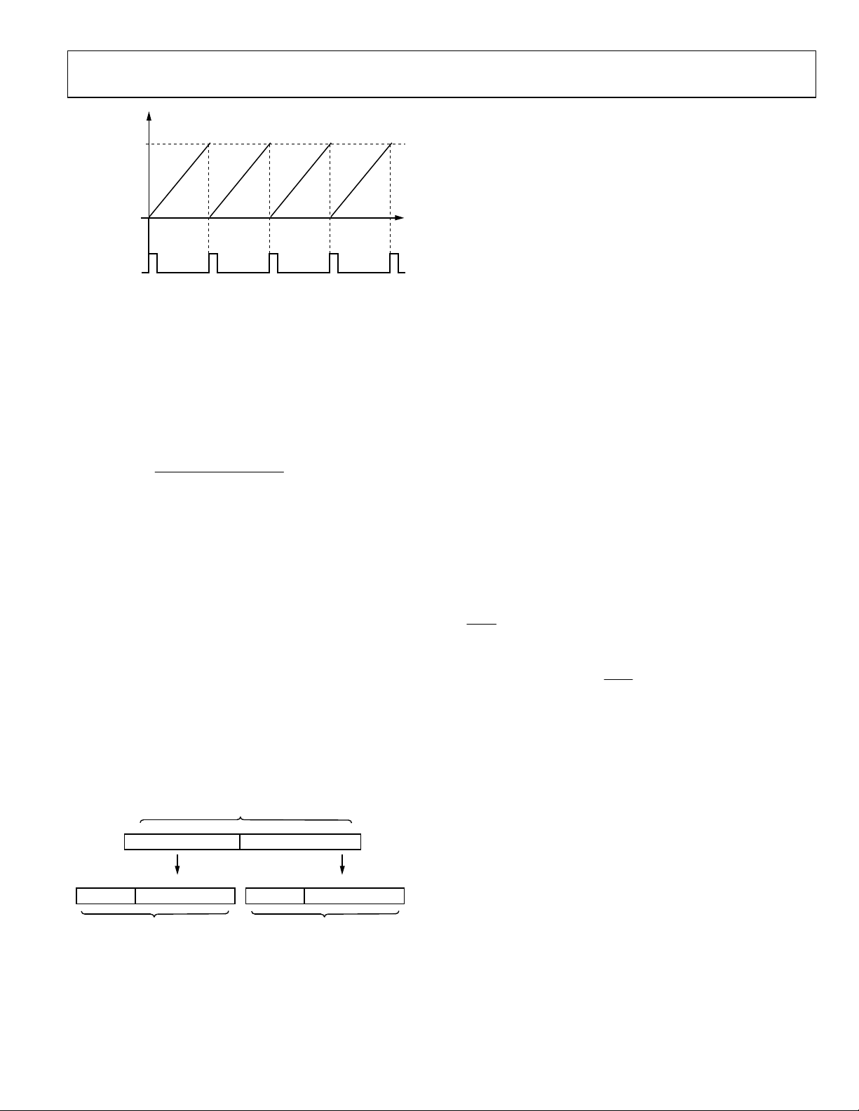
ADE7878
A
ACTIVE POW ER
CCUMULATION
GENERATED
PULSES
WTHR[47:0]
IN DSP
DSP
1 DSP PULSE = 1LSB OF WATTHR[47:0]
Figure 62. Active Power Accumulation Inside DSP
Figure 62 explains this process. The WTHR[47:0] 48-bit signed
register contains the threshold. It is introduced by the user and
is common for all phase total active and fundamental powers.
Its value depends on how much energy is assigned to one LSB
n
of watt-hour registers. Supposing a derivative of wh [10
wh], n
as an integer, is desired as one LSB of the xWATTHR register.
Then WTHR is computed using the following expression:
n
×××
103600
(25)
WTHR
fPMAX
=
S
IU
×
FSFS
where:
PMAX = 33,516,139 = 0x1FF6A6B as the instantaneous power
computed when the ADC inputs are at full scale.
= 8 kHz, the frequency with which the DSP computes the
f
S
instantaneous power.
U
, IFS are the rms values of phase voltages and currents when
FS
the ADC inputs are at full scale.
The maximum value that can be written on WTHR[47:0] is
47
− 1. The minimum value is 0x0, but it is recommended to
2
write a number equal to or greater than PMAX. Never use
negative numbers.
The WTHR[47:0] is a 48-bit register. As previously stated, the
serial ports of the ADE7878 work on 32-, 16-, or 8-bit words.
As shown in Figure 63, the WTHR register is accessed as two
32-bit registers (WTHR1[31:0] and WTHR0[31:0]), each
having eight MSBs padded with 0s.
WTHR[47:0]
47 24
31 24 23 0 31 24 23 0
0000 0000 24 BIT SIGNED NUMBER 0000 0000 24 BIT S IGNED NUMBER
WTHR1[31:0] WTHR0[31: 0]
Figure 63. WTHR[47:0] Communicated As Two 32-Bit Registers
23 0
This discrete time accumulation or summation is equivalent to
integration in continuous time following the description in
Equation 26.
∞
()
∫
Lim
0T
⎧
∑
⎨
n
⎩
()
=→0
⎫
TnTpdttpEnergy (26)
×==
⎬
⎭
where:
n is the discrete time sample number.
T is the sample period.
In the ADE7878, the total phase active powers are accumulated
in the AWATTHR[31:0], BWATTHR[31:0], and CWATTHR[31:0]
32-bit signed registers, and the fundamental phase active powers
08510-045
are accumulated in the AFWATTHR[31:0], BFWATTHR[31:0],
and CFWATTHR[31:0] 32-bit signed registers. The active
energy register content can roll over to full-scale negative
(0x80000000) and continue increasing in value when the active
power is positive. Conversely, if the active power is negative, the
energy register underflows to full-scale positive (0x7FFFFFFF)
and continues decreasing in value.
Bit 0 (AEHF) in the STATUS0[31:0] register is set when Bit 30
of one of the xWATTHR registers changes, signifying that one
of these registers is half full. If the active power is positive, the
watt-hour register becomes half full when it increments from
0x3FFF FFFF to 0x4000 0000. If the active power is negative,
the watt-hour register becomes half full when it decrements
from 0xC000 0000 to 0xBFFF FFFF. Similarly, Bit 1 (FAEHF) in
vSTATUS0[31:0] register is set when Bit 30 of one of the
xFWATTHR registers changes, signifying that one of these
registers is half full.
Setting Bits[1:0] in the MASK0[31:0] register enables the
FAEHF and AEHF interrupts, respectively. If enabled, the
IRQ0
pin is set low and the status bit is set to 1 whenever one
of the energy registers, xWATTHR (for the AEHF interrupt) or
xFWATTHR (for the FAEHF interrupt), become half full. The
status bit is cleared and the
IRQ0
pin is set to logic high by writing
to the STATUS0 register with the corresponding bit set to 1.
Setting Bit 6 (RSTREAD) of the LCYMODE[7:0] register
enables a read-with-reset for all watt-hour accumulation
registers; that is, the registers are reset to 0 after a read
operation.
Integration Time Under Steady Load
The discrete time sample period (T) for the accumulation register
is 125 µs (8 kHz frequency). With full-scale sinusoidal signals
on the analog inputs and the watt gain registers set to 0x00000, the
average word value from each LPF2 is PMAX = 33,516,139 =
0x1FF6A6B. If the WTHR[47:0] threshold is set at the PMAX
08510-046
level, this means that the DSP generates a pulse that is added to
the watt-hour registers every 125 µs.
The maximum value that can be stored in the watt-hour
accumulation register before it overflows is 2
31
− 1 or
0x7FFFFFFF. The integration time is calculated as
Time = 0x7FFF,FFFF × 125 s = 74 hr 33 min 55 sec (27)
Rev. 0 | Page 45 of 92

ADE7878
Energy Accumulation Modes
The active power accumulated in each watt-hour accumulation
32-bit reg ister (AWATTHR, BWATT HR, C WAT THR , AFWATTHR,
BFWATTHR, and CFWATTHR) depends on the configuration of
Bit 5 and Bit 4 (CONSEL bits) in the ACCMODE[7:0] register. The
various configurations are described in Table 14.
Table 14. Inputs to Watt-Hour Accumulation Registers
CO NSEL AWATTHR BWATTHR CWAT THR
00 VA × IA VB × IB VC × IC
01 VA × IA 0 VC × IC
10 VA × IA VB × IB VC × IC
VB = −VA − VC
11 VA × IA VB × IB VC × IC
VB = −VA
cycles, as shown in Figure 64. The number of half-line cycles is
specified in the LINECYC[15:0] register.
ZXSEL[0] I N
LCYCMODE[7:0]
ZERO
CROSSING
DETECTIO N
(PHASE A)
ZERO
CROSSING
DETECTIO N
(PHASE B)
ZERO
CROSSING
DETECTIO N
(PHASE C)
ZXSEL[1] I N
LCYCMODE[7:0]
ZXSEL[2] I N
LCYCMODE[7:0]
LINECYC[15:0]
CALIBR ATION
CONTROL
Depending on the polyphase meter service, choose the appropriate
formula to calculate the active energy. The American ANSI
C12.10 standard defines the different configurations of the
meter. Tabl e 15 describes which mode should be chosen in
these various configurations.
Table 15. Meter Form Configuration
ANSI Meter Form Configuration CONSEL
5S/13S 3-wire delta 01
6S/14S 4-wire wye 10
8S/15S 4-wire delta 11
9S/16S 4-wire wye 00
Bits[1:0] (WATTACC[1:0]) in the ACCMODE[7:0] register
determine how the CF frequency output can be generated as a
function of the total and fundamental active powers. Whereas
the watt-hour accumulation registers accumulate the active
power in a signed format, the frequency output can be
generated in signed mode or in absolute mode as a function
of the WATTACC[1:0] bits. See the Energy-to-Frequency
Conversion section for details.
Line Cycle Active Energy Accumulation Mode
In line cycle energy accumulation mode, the energy accumulation is synchronized to the voltage channel zero crossings such
that active energy is accumulated over an integral number of
half-line cycles. The advantage of summing the active energy
over an integer number of line cycles is that the sinusoidal component in the active energy is reduced to 0. This eliminates any
ripple in the energy calculation and allows the energy to be
accumulated accurately over a shorter time. By using the line
cycle energy accumulation mode, the energy calibration can be
greatly simplified, and the time required to calibrate the meter
can be significantly reduced. In line cycle energy accumulation
mode, the ADE7878 transfers the active energy accumulated in the
32-bit internal accumulation registers into the xWATHHR[31:0] or
xFWATTHR[31:0] register after an integral number of line
OUTPUT
FROM
LPF2
AWG AINAWAT TOS
ACCUMUL ATOR
WTHR[47:0]
Figure 64. Line Cycle Active Energy Accumulation Mode
AWATTHR[31:0]
32 BIT
REGISTER
The line cycle energy accumulation mode is activated by setting
Bit 0 (LWATT) in the LCYCMODE[7:0] register. The energy accumulation over an integer number of half-line cycles is written
to the watt-hour accumulation registers after LINECYC[15:0]
number of half-line cycles are detected. When using the line
cycle accumulation mode, the Bit 6 (RSTREAD) of the
LCYCMODE[7:0] register should be set to Logic 0 because
the read with reset of watt-hour registers is not available in
this mode.
Phase A, Phase B, and Phase C zero crossings are, respectively,
included when counting the number of half-line cycles by setting
Bits[5:3] (ZXSEL) in the LCYCMODE[7:0] register. Any combination of the zero crossings from all three phases can be used
for counting the zero crossing. Select only one phase at a time
for inclusion in the zero crossings count during calibration.
The number of zero crossings is specified by the LINECYC[15:0]
16-bit unsigned register. The ADE7878 can accumulate active
power for up to 65,535 combined zero crossings. Note that the
internal zero-crossing counter is always active. By setting Bit 0
(LWATT) in the LCYCMODE[7:0] register, the first energy
accumulation result is, therefore, incorrect. Writing to the
LINECYC[15:0] register when the LWATT bit is set resets the
zero-crossing counter, thus ensuring that the first energy
accumulation result is accurate.
At the end of an energy calibration cycle, Bit 5 (LENERGY) in
the STATUS0[31:0] register is set. If the corresponding mask bit
in the MASK0[31:0] interrupt mask register is enabled, the
IRQ0
pin also goes active low. The status bit is cleared and the
08510-047
Rev. 0 | Page 46 of 92

ADE7878
IUU
IRQ0
pin is set to high again by writing to the STATUS0
register with the corresponding bit set to 1.
Because the active power is integrated on an integer number of
half-line cycles in this mode, the sinusoidal components are
reduced to 0, eliminating any ripple in the energy calculation.
Therefore, total energy accumulated using the line cycle
accumulation mode is
+
nTt
()
∫
t
∑
k
∞
1
=
()
−==
cos
γIVnTdttpe (28)
kkkk
where nT is the accumulation time.
Note that line cycle active energy accumulation uses the same
signal path as the active energy accumulation. The LSB size of
these two methods is equivalent.
REACTIVE POWER CALCULATION
The ADE7878 computes the total reactive power on every
phase. Total reactive power integrates all fundamental and
harmonic components of the voltages and currents. ADE7878
also computes the fundamental reactive power, the power
determined only by the fundamental components of the
voltages and currents.
A load that contains a reactive element (inductor or capacitor)
produces a phase difference between the applied ac voltage and
the resulting current. The power associated with reactive elements
is called reactive power, and its unit is VAR. Reactive power is
defined as the product of the voltage and current waveforms when
all harmonic components of one of these signals are phase
shifted by 90°.
Equation 31 gives an expression for the instantaneous reactive
power signal in an ac system when the phase of the current
channel is shifted by +90°.
∞
=
∞
∑
k
k
1
=
iʹ(t) is the current waveform with all harmonic
where
components phase shifted by 90°.
Next, the instantaneous Reactive Power
q(t) = v(t) × iʹ(t) (31)
∞
∑
k
mk
1,
≠=mk
2)(
Vtv sin(kωt + φ
∑
k
=
1
k
∑
k
∞
=
1
∞
∑
=
1
k
IV
m
()
sin2)(
k
⎛
sin2)('
⎜
⎝
×=
2)(
IVtq sin(kωt + φ
kk
kωt + φ
× 2sin(
) (29)
k
γtωkIti +=
(30)
k
π
⎞
++=
γtωkIti
⎟
k
2
⎠
q(t) can be expressed as
) × sin(kωt + γk +
k
) × sin(mωt + γm +
k
π
) +
2
π
)
2
∞
=1)(
IVtq {cos(φ
∑
kk
=
k
∞
IV
∑
mk
≠=mk
{cos[(k – m)ωt + φ
m
k
1,
k
− γk −
π
) − cos(2 kωt + φ
2
− γk −
k
π
]} (32)
2
+ γk +
k
π
2
)} +
The average total reactive power over an integral number of line
cycles (n) is given by the expression in Equation 33.
nT
1
∫
nT
0
∞
=
IVQ sin(φ
∑
kk
1k
=
()
∞
==
dt
∑
k
=
1
– γk)
k
IVtqQ cos(φ
kk
k
– γk −
π
) (33)
2
where:
T is the period of the line cycle.
Q is referred to as the total reactive power. Note that the total
reactive power is equal to the dc component of the instantaneous
reactive power signal q(t) in Equation 32, that is,
∞
IV sin(φk – γk)
∑
kk
=1k
This is the relationship used to calculate the total reactive power
in the ADE7878 for each phase. The instantaneous reactive
Power Signal q(t) is generated by multiplying each harmonic of
the voltage signals by the 90° phase-shifted corresponding
harmonic of the current in each phase.
The ADE7878 stores the instantaneous total phase reactive
powers into the AVAR[23:0], BVAR[23:0], and CVAR[23:0]
registers. Their expression is
xVAR sin(φk – γk) × PMAX ×
∑
∞
1k
=
k
k
××=
I
FS
FS
1
(34)
4
2
where:
, IFS are the rms values of the phase voltage and current when
U
FS
the ADC inputs are at full scale.
PMAX = 33,516,139, the instantaneous power computed when
the ADC inputs are at full scale and in phase.
The xVAR[23:0] waveform registers can be accessed using
various serial ports. Refer to the Wav e for m Sa mpli ng Mo de
section for more details.
The expression of fundamental reactive power is obtained from
Equation 37 with k = 1, as follows:
FQ = V
cos(φ1 – γ1)
1I1
The ADE7878 computes the fundamental reactive power using
a proprietary algorithm that requires some initialization function
of the frequency of the network and its nominal voltage measured
in the voltage channel. These initializations are introduced in
the Active Power Calculation section and are common for both
fundamental active and reactive powers.
Note that
q(t) can be rewritten as
Rev. 0 | Page 47 of 92

ADE7878
Tabl e 16 presents the settling time for the fundamental reactive
power measurement, which is the time it takes the power to
reflect the value at the input of theADE7878.
Table 16. Settling Time for Fundamental Reactive Power
Input Signals
63% Full Scale 100% Full Scale
375 ms 875 ms
Reactive Power Gain Calibration
The average reactive power from the LPF output in each phase
can be scaled by ±100% by writing to the phase’s VAR gain 24-bit
register (AVARGAIN[23:0], BVARGAIN[23:0], CVARGAIN[23:0],
AFVARGAIN[23:0], BFVARGAIN[23:0], or CFVARGAIN[23:0]).
The xVARGAIN registers are placed in each phase of the total
reactive power datapath. The xFVARGAIN registers are placed in
each phase of the fundamental reactive power datapath. The
xVARGAIN registers are twos complement signed registers and
have a resolution of 2
registers is expressed by
OutputLPF
e output is scaled by –50% by writing 0xC00000 to the
Th
xVARGAIN registers and increased by +50% by writing
0x400000 to them. These registers can be used to calibrate the
reactive power (or energy) gain in the ADE7878 for each phase.
As previously stated, the serial ports of the ADE7878 work on
32-, 16-, or 8-bit words, and the DSP works on 28 bits. Similar
to registers presented in Figure 32, the AVARGAIN,
BVARGAIN, CVARGAIN, AFVARGAIN, BFVARGAIN, and
CFVARGAIN 24-bit signed registers are accessed as 32-bit
registers with the four MSBs padded with 0s and sign extended
to 28 bits.
Reactive Power Offset Calibration
The ADE7878 provides a reactive power offset register on
each phase and on each reactive power. The AVAROS[23:0],
BVAROS[23:0], and CVAROS[23:0] registers compensate the
offsets in the total reactive power calculations, whereas the
AFVAROS[23:0], BFVAROS[23:0], and CFVAROS[23:0]
registers compensate offsets in the fundamental reactive power
calculations. These are signed twos complement 24-bit registers
that are used to remove offsets in the reactive power
calculations. An offset can exist in the power calculation due to
crosstalk between channels on the PCB or in the chip itself. The
offset calibration allows the contents of the reactive power
register to be maintained at 0 when no reactive power is being
consumed. The offset resolution of the registers is the same as
for the active power offset registers (see the Active Power Offset
Calibration section).
−23
/LSB. The function of the xVARGAIN
=
PowerReactiveAverage
(35)
⎛
+×
12
⎜
⎝
gisterRexVARGAIN
⎞
23
2
⎟
⎠
As previously stated, the serial ports of the ADE7878 work on
32-, 16-, or 8-bit words, and the DSP works on 28 bits. Similar
to registers presented in Figure 32, the AVAROS, BVAROS, and
CVAROS 24-bit signed registers are accessed as 32-bit registers
with the four MSBs padded with 0s and sign extended to 28 bits.
Sign of Reactive Power Calculation
Note that the reactive power is a signed calculation. Tabl e 17
summarizes the relationship between the phase difference between
the voltage and the current and the sign of the resulting reactive
power calculation.
The ADE7878 has a sign detection circuitry for reactive power
calculations. It can monitor the total reactive powers or the
fundamental reactive powers. As described in the Reactive
Energy Calculation section, the reactive energy accumulation is
executed in two stages. Every time a sign change is detected in
the energy accumulation at the end of the first stage, that is,
after the energy accumulated into the 48-bit accumulator
reaches the VARTHR[47:0] register threshold, a dedicated
interrupt is triggered. The sign of each phase reactive power can
be read in the PHSIGN[15:0] register. Bit 7 (REVRPSEL) in the
ACCMODE[7:0] register sets the type of reactive power being
monitored. When REVRPSEL is 0, the default value, the total
reactive power is monitored. When REVRPSEL is 1, then the
fundamental reactive power is monitored.
Bits[12:10] (REVRPC, REVRPB, and REVRPA, respectively)
in the STATUS0[31:0] register are set when a sign change
occurs in the power selected by Bit 7 (REVRPSEL) in the
ACCMODE[7:0] register.
Bits[6:4] (CVARSIGN, BVARSIGN, and AVARSIGN, respectively)
in the PHSIGN[15:0] register are set simultaneously with the
REVRPC, REVRPB, and REVRPA bits. They indicate the sign of
the reactive power. When they are 0, the reactive power is
positive. When they are 1, the reactive power is negative.
Bit REVRPx in the STATUS0[31:0] register and Bit xVARSIGN
in the PHSIGN[15:0] register refer to the reactive power of
Phase x, the power type being selected by Bit REVRPSEL in
ACCMODE[7:0] register.
Setting Bits[12:10] in the MASK0[31:0] register enables the
REVRPC, REVRPB, and REVRPA interrupts, respectively. If
enabled, the
IRQ0
pin is set low and the status bit is set to 1
whenever a change of sign occurs. To find the phase that
triggered the interrupt, the PHSIGN[15:0] register is read
immediately after reading the STATUS0[31:0] register. Next, the
status bit is cleared and the
IRQ0
pin is set to high by writing to
the STATUS0 register with the corresponding bit set to 1.
Rev. 0 | Page 48 of 92

ADE7878
Table 17. Sign of Reactive Power Calculation
Φ1 Integrator Sign of Reactive Power
Between 0 to +90 Off Positive
Between −90 to 0 Off Negative
Between 0 to +90 On Positive
Between −90 to 0 On Negative
1
Φ is defined as the phase angle of the voltage signal minus the current
signal; that is, Φ is positive if the load is inductive and negative if the load is
capacitive.
Reactive Energy Calculation
Reactive energy is defined as the integral of reactive power.
Reactive Energy = ∫q(t)dt (36)
Both total and fundamental reactive energy accumulations are
always a signed operation. Negative energy is subtracted from
the reactive energy contents.
Similar to active power, the ADE7878 achieves the integration
of the reactive power signal in two stages (see Figure 65). The
process is identical for both total and fundamental active
powers.
•
The first stage is conducted inside the DSP: every 125 µs
(8 kHz frequency), the instantaneous phase total reactive
or fundamental power is accumulated into an internal
register. When a threshold is reached, a pulse is generated
at processor port and the threshold is subtracted from the
internal register. The sign of the energy in this moment is
considered the sign of the reactive power (see the Sign of
Reactive Power Calculation section for details).
•
The second stage is done outside the DSP and consists of
accumulating the pulses generated by the processor into
internal 32-bit accumulation registers. The content of these
registers is transferred to the var-hour registers (Registers
xVARHR[31:0] and xFVARHR[31:0]) when these registers
are accessed. AVARHR[31:0], BVARHR[31:0],
CVARHR[31:0], AFWATTHR[31:0], BFWATTHR[31:0],
and CFWATTHR[31:0] represent phase fundamental
reactive powers.
Figure 62 in the Active Energy Calculation section explains this
process. The VARTHR[47:0] 48-bit signed register contains the
threshold, and it is introduced by the user. It is common for
both total and fundamental phase reactive powers. Its value
depends on how much energy is assigned to one LSB of varhour registers. Supposing a derivative of a volt ampere reactive
hour (varh) at [10
n
varh] where n is an integer is desired as one
LSB of the VARHR register. Then, the VARTHR register can be
computed using the following equation:
n
⋅××
103600
FSFS
VARTHR
fPMAX
=
s
IU
×
where:
PMAX = 33,516,139 = 0x1FF6A6B, the instantaneous power
computed when the ADC inputs are at full scale.
f
= 8 kHz, the frequency with which the DSP computes the
S
instantaneous power.
U
, IFS are the rms values of phase voltages and currents when
FS
the ADC inputs are at full scale.
The maximum value that may be written on VARTHR[47:0] is
47
− 1. The minimum value is 0x0, but it is recommended to
2
write a number equal to or greater than PMAX. Never use
negative numbers.
The VARTHR[47:0] is a 48-bit register. As previously stated, the
serial ports of the ADE7878 work on 32-, 16-, or 8-bit words.
Similar to the WTHR[47:0] register shown in Figure 63,
VARTHR[47:0] is accessed as two 32-bit registers
(VARTHR1[31:0] and VARTHR0[31:0]), each having eight MSBs
padded with 0s.
This discrete time accumulation or summation is equivalent to
integration in continuous time following the expression in
Equation 37
Re
∞
()
∫
Lim
→
0T
⎧
∑
⎨
n
=
⎩
()
0
⎫
TnTqdttqgyactiveEner (37)
×==
⎬
⎭
where:
n is the discrete time sample number.
T is the sample period.
On the ADE7878, the total phase reactive powers are
accumulated in the AVARHR[31:0], BVARHR[31:0], and
CVARHR[31:0] 32-bit signed registers. The fundamental phase
reactive powers are accumulated in the AFVARHR[31:0],
BFVARHR[31:0], and CFVARHR[31:0] 32-bit signed registers.
The reactive energy register content can roll over to full-scale
negative (0x80000000) and continue increasing in value when
the reactive power is positive. Conversely, if the reactive power
is negative, the energy register underflows to full-scale positive
(0x7FFFFFFF) and continues to decrease in value.
Bit 2 (REHF) in the STATUS0[31:0] register is set when Bit 30
of one of the xVARHR registers changes, signifying that one of
these registers is half full. If the reactive power is positive, the
var-hour register becomes half full when it increments from
0x3FFF FFFF to 0x4000 0000. If the reactive power is negative,
the var-hour register becomes half full when it decrements from
0xC000 0000 to 0xBFFF FFFF. Analogously, Bit 3 (FREHF) in the
STATUS0[31:0] register is set when Bit 30 of one of the
xFVARHR registers changes, signifying that one of these
registers is half full.
Setting Bits[3:2] in the MASK0[31:0] register enables the
FREHF and REHF interrupts, respectively. If enabled, the
IRQ0
pin is set low and the status bit is set to 1 whenever one of the
Rev. 0 | Page 49 of 92

ADE7878
energy registers, xVARHR (for REHF interrupt) or xFVARHR
(for FREHF interrupt), becomes half full. The status bit is
cleared and the
STATUS0 register with the corresponding bit set to 1.
IRQ0
pin is set to high by writing to the
Setting Bit 6 (RSTREAD) of LCYMODE[7:0] register enables a
read-with-reset for all var-hour accumulation registers, that is,
the registers are reset to 0 after a read operation.
IA
VA
APHCAL
AIGAIN
AVGAIN
HPFDIS
[23:0]
HPF
HPFDIS
[23:0]
HPF
DIGITAL
INTEGRATOR
ALGORITHM
DIGITAL SIGNAL PROCESSOR
TOTAL
REACTIVE
POWER
AVAROS
AVARGAIN
ACCUMULATOR
VARTHR[47:0]
REVRPA BIT IN
STATUS0[31:0]
AV ARHR[31:0]
32 BIT
REGISTER
08510-245
Figure 65. Total Reactive Energy Accumulation
Rev. 0 | Page 50 of 92

ADE7878
Integration Time Under a Steady Load
The discrete time sample period (T) for the accumulation
register is 125 µs (8 kHz frequency). With full-scale pure
sinusoidal signals on the analog inputs and a 90° phase
difference between the voltage and the current signal (the
largest possible reactive power), the average word value
representing the reactive power is PMAX = 33,516,139 =
0x1FF6A6B. If the VARTHR[47:0] threshold is set at the PMAX
level, this means that the DSP generates a pulse that is added at
the var-hour registers every 125 µs.
The maximum value that can be stored in the var-hour accumulation register before it overflows is 2
31
− 1 or 0x7FFFFFFF. The
integration time is calculated as
Time = 0x7FFF,FFFF × 125 s = 74 hr 33 min 55 sec (38)
Energy Accumulation Modes
The reactive power accumulated in each var-hour accumulation
32-bit register (AVARHR, BVARHR, CVARHR, AFVARHR,
BFVARHR, and CFVARHR) depends on the configuration of
Bits[5:4] (CONSEL) in the ACCPMODE[7:0] register, in
correlation with the watt-hour registers. The different
configurations are described in Tabl e 18 . Note that IA
’/IB’/IC’
are the phase-shifted current waveforms.
Table 18. Inputs to Var-Hour Accumulation Registers
CONSEL[1,0]
AVAR HR ,
AFVARHR
BVARHR,
BFVARHR
CVARHR,
CFVARHR
00 VA × IA’ VB × IB’ VC × IC’
01 VA × IA’ 0 VC × IC’
10 VA × IA’ VB × IB’ VC x IC’
VB = −VA − VC
11 VA × IA’ VB × IB’ VC × IC’
VB = −VA
Bits[3:2] (VARACC[1:0]) in the ACCMODE[7:0] register
determine how CF frequency output can be a generated
function of the total active and fundamental powers. While the
var-hour accumulation registers accumulate the reactive power
in a signed format, the frequency output may be generated in
either the signed mode or the sign adjusted mode function of
VARACC[1:0]. See the Energy-to-Frequency Conversion
section for details.
Line Cycle Reactive Energy Accumulation Mode
As mentioned in the Line Cycle Active Energy Accumulation
Mode section, in-line cycle energy accumulation mode, the
energy accumulation can be synchronized to the voltage
channel zero crossings so that reactive energy can be
accumulated over an
integral number of half-line cycles. In this mode, the ADE7878
transfers the reactive energy accumulated in the 32-bit internal
accumulation registers into the xVARHR[31:0] or xFVAR[31:0]
register after an integral number of line cycles, as shown in
Figure 66. The number of half-line cycles is specified in the
LINECYC[15:0] register.
The line cycle reactive energy accumulation mode is activated
by setting Bit 1 (LVAR) in the LCYCMODE[7:0] register. The
total reactive energy accumulated over an integer number of
half-line cycles or zero crossings is accumulated in the var-hour
accumulation registers after the number of zero crossings
specified in the LINECYC register is detected. When using the
line cycle accumulation mode, Bit 6 (RSTREAD) of the
LCYCMODE[7:0] register should be set to Logic 0 because a
read with the reset of var-hour registers is not available in this
mode.
ZXSEL[0] I N
LCYCMODE[7:0]
ZERO-
CROSSING
DETECTIO N
(PHASE A)
ZXSEL[1] I N
LCYCMODE[7:0]
ZERO-
CROSSING
DETECTIO N
(PHASE B)
ZXSEL[2] I N
LCYCMODE[7:0]
ZERO-
CROSSING
DETECTIO N
(PHASE C)
AVAROS
AVARG AI N
OUTPUT
FROM
TOTAL
REACTIVE
POWER
ALGORI THM
Figure 66. Line Cycle Reactive Energy Accumulation Mode
ACCUMUL ATOR
VARHR[47:0]
LINECYC[15:0]
CALIBR ATION
CONTROL
AVARHR[31:0]
REGISTE R
32-BIT
Phase A, Phase B, and Phase C zero crossings are, respectively,
included when counting the number of half-line cycles by
setting Bits[5:3] (ZXSEL) in the LCYCMODE[7:0] register. Any
combination of the zero crossings from all three phases can be
used for counting the zero crossing. Select only one phase at a
time for inclusion in the zero-crossings count during calibration.
For details on setting the LINECYC[15:0] register and Bit 5
(LENERGY) in the MASK0 interrupt mask register associated
with the line cycle accumulation mode, see the Line Cycle
Active Energy Accumulation Mode section.
08510-146
Rev. 0 | Page 51 of 92

ADE7878
IUU
APPARENT POWER CALCULATION
Apparent power is defined as the maximum power that can be
delivered to a load. One way to obtain the apparent power is by
multiplying the voltage rms value by the current rms value (also
called the arithmetic apparent power) as follows:
S = V rms × I rms (39)
where:
S is the apparent power
V rms and I rms are the rms voltage and current, respectively.
The ADE7878 computes the arithmetic apparent power on each
phase. Figure 67 illustrates the signal processing in each phase
for the calculation of the apparent power in the ADE7878.
Because V rms and I rms contain all harmonic information,
the apparent power computed by the ADE7878 is a total apparent
power. The ADE7878 does not compute a fundamental apparent
power because it does not measure the rms values of the fundamental voltages and currents.
The ADE7878 stores the instantaneous phase apparent powers
into the AVA[23:0], BVA[23:0], and CVA[23:0] registers. Their
expression is
1
xVA
I
FSFS
×××= PMAX
(40)
4
2
where:
U, I are the rms values of the phase voltage and current.
U
, IFS are the rms values of the phase voltage and current when
FS
the ADC inputs are at full scale.
PMAX = 33,516,139, the instantaneous power computed when
the ADC inputs are at full scale and in phase.
The xVA[23:0] waveform registers may be accessed using
various serial ports. Refer to the Wavef o rm S ampl ing Mo de
section for more details.
The ADE7878 can compute the apparent power in an alternative
way by multiplying the phase rms current by an rms voltage
introduced externally. See the Apparent Power Calculation
Using VNOM section for details.
AIRMS
AVR MS
AVAGAIN
ACCUMULATOR
VATHR[47:0]
DIGITAL SIGNAL PROCESSOR
Figure 67. Apparent Power Data Flow and Apparent Energy Accumulation
AVAHR[31:0]
32 BIT REGI STER
08510-048
Rev. 0 | Page 52 of 92

ADE7878
r
t
U
Apparent Power Gain Calibration
The average apparent power result in each phase can be scaled
by ±100% by writing to the phase’s VAGAIN 24-bit register
(AVAGAIN[23:0], BVAGAIN[23:0], or CVAG AIN[23:0]). The
VAGAIN registers are twos complement signed registers and
have a resolution of 2
−23
/LSB. The function of the xVAGAIN
registers is expressed mathematically as
Average
Apparen
IrmsVrms
=
Powe
⎛
+××
1
⎜
⎝
RegisterVAGAIN
23
2
(41)
⎞
⎟
⎠
The output is scaled by –50% by writing 0xC00000 to the
xVAGAIN registers and increased by +50% by writing
0x400000 to them. These registers can be used to calibrate the
apparent power (or energy) calculation in the ADE7878 for
each phase.
As previously stated, the serial ports of the ADE7878 work on
32-, 16-, or 8-bit words, and the DSP works on 28 bits. Similar
to registers presented in Figure 32, the AVAGAIN, BVAGAIN,
and CVAGAIN 24-bit registers are accessed as 32-bit registers
with the four MSBs padded with 0s and sign extended to 28 bits.
Apparent Power Offset Calibration
Each rms measurement includes an offset compensation register
to calibrate and eliminate the dc component in the rms value
(see the Root Mean Square Measurement section). The voltage
and current rms values are then multiplied together in the
apparent power signal processing. Because no additional offsets
are created in the multiplication of the rms values, there is no
specific offset compensation in the apparent power signal
processing. The offset compensation of the apparent power
measurement in each phase should be done by calibrating each
individual rms measurement.
Apparent Power Calculation Using VNOM
The ADE7878 can compute the apparent power by multiplying
the phase rms current by an rms voltage introduced externally
in the VNOM[23:0] 24-bit signed register. When one of
Bits[13:11] (VNOMCEN, VNOMBEN, or VNOMAEN) in the
COMPMODE[15:0] register is set to 1, the apparent power in
the corresponding phase (Phase x for VNOMxEN) is computed
in this way. When the VNOMxEN bits are cleared to 0, the
default value, then the arithmetic apparent power is computed.
The VNOM[23:0] register contains a number determined by U,
the desired rms voltage, and U
, the rms value of the phase
FS
voltage when the ADC inputs are at full scale as follows:
(42)
VNOM
U is the nominal phase rms voltage.
where
U
FS
910,191,4×=
As previously stated, the serial ports of the ADE7878 work on
32-, 16-, or 8-bit words. Similar to the register presented in
Figure 33, the VNOM 24-bit signed register is accessed as a
32-bit register with the eight MSBs padded with 0s.
Apparent Energy Calculation
Apparent energy is defined as the integral of apparent power.
Apparent Energy = ∫s(t)dt (43)
Similar to active and reactive powers, the ADE7878 achieves the
integration of the apparent power signal in two stages (see
Figure 67). The first stage is conducted inside the DSP: every
125 μs (8 kHz frequency), the instantaneous phase apparent
power is accumulated into an internal register. When a
threshold is reached, a pulse is generated at the processor port,
and the threshold is subtracted from the internal register. The
second stage is conducted outside the DSP and consists of
accumulating the pulses generated by the processor into
internal 32-bit accumulation registers. The content of these
registers is transferred to the VA-hour registers, xVAHR[31:0],
when these registers are accessed. Figure 62 from the Active
Energy Calculation section illustrates this process. The
VATHR[47:0] 48-bit register contains the threshold. Its value
depends on how much energy is assigned to one LSB of the
VA-hour registers. Supposing a derivative of apparent energy
(VAh) of [10
n
VAh], where n is an integer, is desired as one LSB
of the xVAHR register, then, the xVATHR register can be
computed using the following equation:
n
×××
103600
VATHR
fPMAX
=
s
IU
×
FSFS
where:
PMAX = 33,516,139 = 0x1FF6A6B, the instantaneous power
computed when the ADC inputs are at full scale.
f
= 8 kHz, the frequency with which the DSP computes the
S
instantaneous power.
, IFS are the rms values of the phase voltages and currents
U
FS
when the ADC inputs are at full scale.
VATHR[47:0] is a 48-bit register. As previously stated, the serial
ports of the ADE7878 work on 32-, 16-, or 8-bit words. Similar
to the WTHR[47:0] register presented in Figure 63, VATHR[47:0]
is accessed as two 32-bit registers (VATHR1[31:0] and
VATHR0[31:0]), each having eight MSBs padded with 0s.
This discrete time accumulation or summation is equivalent to
integration in continuous time following the description in
Equation 44.
∞
Lim
0T
⎧
∑
⎨
=→0
n
⎩
()
()
∫
⎫
(44)
×==
TnTsdttsergyApparentEn
⎬
⎭
Rev. 0 | Page 53 of 92

ADE7878
where:
n is the discrete time sample number.
T is the sample period.
In the ADE7878, the phase apparent powers are accumulated in
the AVAHR[31:0], BVAHR[31:0], and CVAHR[31:0] 32-bit
signed registers. The apparent energy register content can roll
over to full-scale negative (0x80000000) and continue increasing
in value when the apparent power is positive. Conversely, if
because of offset compensation in the rms datapath, the apparent
power is negative, the energy register underflows to full-scale
positive (0x7FFFFFFF) and continues to decrease in value.
Bit 4 (VAEHF) in the STATUS0[31:0] register is set when Bit 30
of one of the xVAHR registers changes, signifying that one of
these registers is half full. Because the apparent power is always
positive and the xVAHR registers are signed, the VA-hour registers
become half full when they increment from 0x3FFFFFFF to
0x4000 0000. Interrupts attached to Bit VAEHF in the
STATUS0[31:0] register can be enabled by setting Bit 4 in the
MASK0[31:0] register. If enabled, the
the status bit is set to 1 whenever one of the Energy Registers
xVAHR becomes half full. The status bit is cleared and the
pin is set to high by writing to the STATUS0 register with the
corresponding bit set to 1.
Setting Bit 6 (RSTREAD) of the LCYMODE[7:0] register
enables a read-with-reset for all xVAHR accumulation registers;
that is, the registers are reset to 0 after a read operation.
Integration Time Under Steady Load
The discrete time sample period for the accumulation register is
125 µs (8 kHz frequency). With full-scale pure sinusoidal signals
on the analog inputs, the average word value representing the
apparent power is PMAX. If the VATHR threshold register is set
IRQ0
pin is set low and
ZXSEL[0] I N
LCYCMODE[7:0]
ZERO-
CROSSING
DETECTIO N
(PHASE A)
ZXSEL[1] I N
LCYCMODE[7:0]
ZERO-
CROSSING
DETECTIO N
(PHASE B)
IRQ0
at the PMAX level, this means the DSP generates a pulse that is
added at the xVAHR registers every 125 µs.
The maximum value that can be stored in the xVAHR
accumulation register before it overflows is 2
31
− 1 or
0x7FFFFFFF. The integration time is calculated as
Time = 0x7FFF,FFFF × 125 s = 74 hr 33 min 55 sec (45)
Energy Accumulation Mode
The apparent power accumulated in each accumulation register
depends on the configuration of Bits[5:4] (CONSEL) in the
ACCMODE[7:0] register. The various configurations are
described in Ta b le 1 9.
Table 19. Inputs to VA-Hour Accumulation Registers
CONSEL[1,0] AVAHR BVAHR CVAHR
00 AVRMS × AIRMS BVRMS × BIRMS CVRMS × CIRMS
01 AVRMS × AIRMS 0 CVRMS × CIRMS
10 AVRMS × AIRMS BVRMS × BIRMS
VB = −VA − VC
11 AVRMS × AIRMS BVRMS × BIRMS
VB = −VA
Line Cycle Apparent Energy Accumulation Mode
CVRMS × CIRMS
CVRMS × CIRMS
As described in the Line Cycle Active Energy Accumulation
Mode section, in line cycle energy accumulation mode, the
energy accumulation can be synchronized to the voltage channel
zero crossings allowing apparent energy to be accumulated over an
integral number of half-line cycles. In this mode, the ADE7878
transfers the apparent energy accumulated in the 32-bit internal
accumulation registers into xVAHR[31:0] registers after an
integral number of line cycles, as shown in Figure 68. The
number of half-line cycles is specified in the LINECYC[15:0]
register.
LINECYC[15:0]
CALIBR ATION
CONTROL
ZXSEL[2] I N
LCYCMODE[7:0]
ZERO-
CROSSING
DETECTIO N
(PHASE C)
AVAGAINAIRMS
ACCUMUL ATOR
AVRM S
Figure 68. Line Cycle Apparent Energy Accumulation Mode
VAHR[47:0]
Rev. 0 | Page 54 of 92
AVAHR[31:0]
32-BIT
REGISTER
08510-049

ADE7878
The line cycle apparent energy accumulation mode is activated
by setting Bit 2 (LVA) in the LCYCMODE[7:0] register. The
apparent energy accumulated over an integer number of zero
crossings is written to the xVAHR accumulation registers after
the number of zero crossings specified in the LINECYC register
is detected. When using the line cycle accumulation mode, Bit 6
(RSTREAD) of the LCYCMODE[7:0] register should be set to
Logic 0 because a read with the reset of xVAHR registers is not
available in this mode.
Phase A, Phase B, and Phase C zero crossings are, respectively,
included when counting the number of half-line cycles by
setting Bits[5:3] (ZXSEL) in the LCYCMODE[7:0] register. Any
combination of the zero crossings from all three phases can be
used for counting the zero crossing. Select only one phase at a
time for inclusion in the zero-crossings count during calibration.
For details on setting the LINECYC[15:0] register and Bit 5
(LENERGY) in the MASK0 interrupt mask register associated
with the line cycle accumulation mode, see the Line Cycle
Active Energy Accumulation Mode section.
WAVEFORM SAMPLING MODE
The waveform samples of the current and voltage waveform, the
active, reactive, and apparent power multiplier outputs are
stored every 125 µs (8 kHz rate) into 24-bit signed registers that
can be accessed through various serial ports of the ADE7878.
Tabl e 20 provides the list of registers and their descriptions.
Table 20. Waveform Registers List
Register Description
IAWV Phase A current
VAWV Phase A voltage
IBWV Phase B current
VBWV Phase B voltage
ICWV Phase C current
VCWV Phase C voltage
INWV Neutral current
AVA Phase A apparent power
Register Description
BVA Phase B apparent power
CVA Phase C apparent power
AWATT Phase A active p ower
BWATT Phase B active power
CWATT Phase C active power
AVAR Phase A reac tive power
BVAR Phase B reactive power
CVAR Phase C reactive power
Bit 17 (DREADY) in the STATUS0[31:0] register can be used to
signal when the registers listed in Tabl e 20 can be read using the
2
C or SPI serial port. An interrupt attached to the flag can be
I
enabled by setting Bit 17 (DREADY) in the MASK0[31:0]
register. See the Digital Signal Processor section for more details
on Bit DREADY.
The ADE7878 contains a high speed data capture (HSDC) port
that is specially designed to provide fast access to the waveform
sample registers. Read the HSDC Interface section for more
details.
As previously stated, the serial ports of the ADE7878 work on
32-, 16-, or 8-bit words. All registers listed in Tab le 2 0 are transmitted sign extended from 24 bits to 32 bits (see Figure 34).
ENERGY-TO-FREQUENCY CONVERSION
The ADE7878 provides three frequency output pins: CF1, CF2,
and CF3. The CF3 pin is multiplexed with the HSCLK pin of
the HSDC interface. When HSDC is enabled, the CF3
functionality is disabled at the pin. The CF1 and CF2 pins are
always available. After initial calibration at manufacturing, the
manufacturer or end customer verifies the energy meter
calibration. One convenient way to verify the meter calibration
is to provide an output frequency proportional to the active,
reactive, or apparent power under steady load conditions. This
output frequency can provide a simple, single-wire, optically
isolated interface to external calibration equipment. Figure 69
illustrates the energy-to-frequency conversion in the ADE7878.
INSTANTANEO US
PHASE A ACTIVE
POWER
INSTANTANEO US
PHASE B ACTIVE
POWER
INSTANTANEO US
PHASE C ACTIVE
POWER
DIGITAL SIGNAL
PROCESSOR
TERMSELx BI TS IN
COMPMODE
CFxSEL BITS
IN CFMODE
7
VA
WATT
VAR
FWATT
FVAR
Figure 69. Energy-to-Frequency Conversion
2
ACCUMULATOR
WTHR[47:0]
REVPSUMx BIT O F
STATUS0[31:0]
FREQUENCY
DIVIDER
CFxDEN
7
2
CFx PULSE
OUTPUT
08510-050
Rev. 0 | Page 55 of 92

ADE7878
The DSP computes the instantaneous values of all phase
powers: total active, fundamental active, total reactive,
fundamental reactive, and apparent. The process in which the
energy is sign accumulated in various xWATTHR, xVARHR,
and xVAHR registers has already been described in the energy
calculation sections. In the energy-to-frequency conversion
process, the instantaneous powers are used to generate signals
at the frequency output pins (CF1, CF2, and CF3). One digitalto-frequency converter is used for every CFx pin. Every
converter sums certain phase powers and generates a signal
proportional to the sum. Two sets of bits decide what powers
are converted.
First, Bits[2:0] (TERMSEL1[2:0]), Bits[5:3] (TERMSEL2[2:0]),
and Bits[8:6] (TERMSEL3[2:0]) of the COMPMODE[15:0]
register decide which phases, or which combination of phases,
are added.
The TERMSEL1 bits refer to the CF1 pin, the TERMSEL2 bits
refer to the CF2 pin, and the TERMSEL3 bits refer to the CF3
pin. The TERMSELx[0] bits manage Phase A. When set to 1,
Phase A power is included in the sum of powers at the CFx
converter. When cleared to 0, Phase A power is not included.
The TERMSELx[1] bits manage Phase B, and the TERMSELx[2]
bits manage Phase C. Setting all TERMSELx bits to 1 means all
3-phase powers are added at the CFx converter. Clearing all
TERMSELx bits to 0 means no phase power is added and no CF
pulse is generated.
Second, Bits[2: 0] (CF1SEL[2:0]), Bits[5:3] (CF2SEL[2:0]), and
Bits[8:6] (CF3SEL[2:0]) in the CFMODE[15:0] register decide
what type of power is used at the inputs of the CF1, CF2, and
CF3 converters, respectively. Ta b le 2 1 shows the values that
CFxSEL can have: total active, total reactive, apparent,
fundamental active, or fundamental reactive powers.
By default, the TERMSELx bits are all 1 and the CF1SEL bits are
000, the CF2SEL bits are 001, and the CF3SEL bits are 010. This
means that by default, the CF1 digital-to-frequency converter
produces signals proportional to the sum of all 3-phase total
active powers, CF2 produces signals proportional to total
reactive powers, and CF3 produces signals proportional to
apparent powers.
Table 21. CFxSEL Bits Description
Registers
Latched When
CFxSEL Description
000 CFx signal proportional to the
sum of total phase active
powers
001 CFx signal proportional to the
sum of total phase reactive
powers
010 CFx signal proportional to the
sum of phase apparent powers
011 CFx signal proportional to the
sum of fundamental phase
active powers
100 CFx signal proportional to the
sum of fundamental phase
reactive powers
101 to
111
Reserved
CFxLATCH = 1
AWATT HR,
BWATTHR,
CWATTHR
AVARHR, BVARHR,
CVARHR
AVAHR, BVAHR,
CVAHR
AFWATTHR,
BFWATTHR,
CFWATTHR
AFVARHR,
BFVARHR,
CFVARHR
Similar to the energy accumulation process, the energy-tofrequency conversion is accomplished in two stages. In the first
stage, the instantaneous phase powers obtained from the DSP at
the 8 kHz rate are shifted left by seven bits and then accumulate
into an internal register at a 1 MHz rate. When a threshold is
reached, a pulse is generated, and the threshold is subtracted
from the internal register. The sign of the energy in this
moment is considered the sign of the sum of phase powers (see
the Sign of Sum-of-Phase Powers in the CFx Datapath section
for details). The threshold is the same threshold used in various
active, reactive, and apparent energy accumulators in the DSP,
WTHR[47:0], VARTHR[47:0], or VATHR[47:0] registers but
this time it is shifted left by seven bits. The advantage of
accumulating the instantaneous powers at the 1 MHz rate
is that the ripple at the CFx pins is greatly diminished.
The second stage consists of the frequency divider by
CFxDEN[15:0] 16-bit unsigned registers. The values of
CFxDEN depend on the meter constant (MC), measured in
impulses/kWh and how much energy is assigned to one LSB of
various energy registers: xWATTHR, xVARHR, and so forth.
Supposing a derivative of wh [10
n
wh], n a positive or negative
integer, is desired as one LSB of the xWATTHR register. Then,
CFxDEN is as follows:
3
CFxDEN
=
MC
10
(46)
n
10]imp/kwh[
×
Rev. 0 | Page 56 of 92

ADE7878
V
A
The derivative of wh must be chosen in such a way to obtain a
CFxDEN register content greater than 1. If CFxDEN = 1, then
the CFx pin stays active low for only 1 µs; therefore, avoid this
number. The frequency converter cannot accommodate fractional
results; the result of the division must be rounded to the nearest
integer. If CFxDEN is set equal to 0, then the ADE7878 considers it
to be equal to 1.
The pulse output for all digital-to-frequency converters stays
low for 80 ms if the pulse period is larger than 160 ms (6.25
Hz). If the pulse period is smaller than 160 ms and CFxDEN is
an even number, the duty cycle of the pulse output is exactly
50%. If the pulse period is smaller than 160 ms and CFxDEN is
an odd number, the duty cycle of the pulse output is
(1+1/CFxDEN) × 50%
The pulse output is active low and preferably connected to an
LED, as shown in Figure 70.
Bits[11:9] (CF3DIS, CF2DIS, and CF1DIS) of the
CFMODE[15:0] register decide if the frequency converter
output is generated at the CF3, CF2, or CF1 pin. When
Bit CFxDIS is set to 1 (the default value), the CFx pin is disabled
and the pin stays high. When Bit CFxDIS is cleared to 0, the
correspondent CFx pin output generates an active low signal.
Bits[16:14] (CF3, CF2, CF1) in the Interrupt Mask Register
MASK0[31:0] manage the CF3, CF2, and CF1 related
interrupts. When the CFx bits are set (whenever a high to low
transition at the corresponding frequency converter output
occurs), an interrupt
IRQ0
is triggered and a status bit in the
STATUS0[31:0] register is set to 1. The interrupt is available
even if the CFx output is not enabled by the CFxDIS bits in the
CFMODE[15:0] register.
DD
for CF1SEL[2:0] = 010 (apparent powers contribute at the CF1
pin) and CFCYC = 2.
The CFCYC[7:0] 8-bit unsigned register contains the number of
high-to-low transitions at the frequency converter output
between two consecutive latches. Writing a new value into the
CFCYC[7:0] register during a high-to-low transition at any CFx
pin should be avoided.
CF1 PULSE
BASED ON
PHASE A AND
PHASE B
APPARENT
POWERS
AVAHR, BVAHR,
CVAHR LATCHED
ENERGY REGISTERS
RESET
Figure 71. Synchronizing AVAHR and BVAHR with CF1
CFCYC = 2
AVAHR, BVAHR,
CVAHR LATCHED
ENERGY REGISTERS
RESET
Bits[14:12] (CF3LATCH, CF2LATCH and CF1LATCH) of the
CFMODE[15:0] register enable this process when set to 1.
When cleared to 0, the default state, no latch occurs. The
process is available even if the CFx output is not enabled by the
CFxDIS bits in the CFMODE[15:0] register.
CF Outputs for Various Accumulation Modes
Bits[1:0] (WATTACC[1:0]) in the ACCMODE[7:0] register
determine the accumulation modes of the total active and
fundamental powers when signals proportional to the active
powers are chosen at the CFx pins (Bit CFxSEL[2:0] in the
CFMODE[15:0] register equals 000 or 011). When
WATTACC[1:0] = 00 (the default value), the active powers are
sign accumulated before entering the energy-to-frequency
converter. Figure 72 shows how signed active power
accumulation works. Note that in this mode, the CFx pulses are
synchronized perfectly with the active energy accumulated in
xWATTHR registers because the powers are sign accumulated
in both datapaths.
08510-052
CFx PIN
CTIVE ENERGY
08510-051
Figure 70. CFx Pin Recommended Connection
Synchronizing Energy Registers with CFx Outputs
The ADE7878 contains a feature that allows synchronizing the
content of phase energy accumulation registers with the
generation of a CFx pulse. When a high-to-low transition at one
frequency converter output occurs, the content of all internal
phase energy registers that relate to the power being output at
CFx pin is latched into hour registers and then resets to 0. See
NO-LOAD
THRESHOLD
ACTIVE POWE R
NO-LOAD
THRESHOLD
REVAPx BIT
IN STATUS0
xWSIGN BIT
IN PHSIGN
Tabl e 21 for the list of registers that are latched based on the
CFxSEL[2:0] bits in the CFMODE[15:0] register. All 3-phase
registers are latched independent of the TERMSELx bits of the
APNOLOAD
SIGN = POSIT IVE
Figure 72. Active Power Signed Accumulation Mode
NEG
NEGPOSPOS
08510-053
COMPMODE[15:0] register. The process is shown in Figure 71
Rev. 0 | Page 57 of 92

ADE7878
A
x
x
When WATTACC[1:0] = 11, the active powers are accumulated
in absolute mode. When the powers are negative, they change
sign and accumulate together with the positive power. Figure 73
shows how absolute active power accumulation works. Note
that in this mode, the xWATTHR registers continue to accumulate
active powers in signed mode, even if the CFx pulses are
generated based on the absolute accumulation mode.
Bits[3:2] (VARACC[1:0]) in the ACCMODE[7:0] register determine the accumulation modes of the total and fundamental
reactive powers when signals proportional to the reactive powers
are chosen at the CFx pins (Bit CFxSEL[2:0] in the CFMODE[15:0]
register equals 001 or 100). When VARACC[1:0] = 00, the
default value, the reactive powers are sign accumulated before
entering the energy-to-frequency converter. Figure 74 shows
how signed reactive power accumulation works. Note that in
this mode, the CFx pulses are synchronized perfectly with the
reactive energy accumulated in the xVARHR registers because
the powers are sign accumulated in both datapaths.
CTIVE ENERGY
NO-LOAD
THRESHOLD
REACTIVE
ENERGY
NO-LOAD
THRESHOLD
REACTIVE
POWER
NO-LOAD
THRESHOLD
REVRPx BIT
IN STATUS0
VARSIGN BIT
IN PHSIGN
VARNOLOAD
SIGN = POSITIVE
NEG
NEGPO SPOS
08510-153
Figure 74. Reactive Power Signed Accumulation Mode
When VARACC[1:0] = 10, the reactive powers are accumulated
depending on the sign of the corresponding active power. If the
active power is positive, the reactive power is accumulated as is.
If the active power is negative, the sign of the reactive power is
changed for accumulation. Figure 75 shows how the sign
adjusted reactive power accumulation mode works. Note that in
this mode, the xVARHR registers continue to accumulate
reactive powers in signed mode, even if the CFx pulses are
generated based on the sign adjusted accumulation mode.
ACTIVE POWE R
NO-LOAD
THRESHOLD
REVAPx BIT
IN STATUS0
xWSIGN BIT
IN PHSIGN
APNOLOAD
SIGN = POSITIVE
Figure 73. Active Power Absolute Accumulation Mode
NEG
REACTIVE
ENERGY
NO-LOAD
THRESHOLD
REACTIVE
POWER
NO-LOAD
THRESHOLD
NO-LOAD
NEGPOSPOS
08510-054
THRESHOLD
ACTIVE
POWER
REVRPx BIT
IN STATUS0
VARSIGN BIT
IN PHSIGN
VARNOLOAD
SIGN = POSIT IVE
NEG
POSPOS
08510-155
Figure 75. Reactive Power Accumulation in Sign Adjusted Mode
Rev. 0 | Page 58 of 92

ADE7878
I
U
Sign of Sum-of-Phase Powers in the CFx Datapath
The ADE7878 has a sign detection circuitry for the sum of
phase powers that are used in the CFx datapath. As seen in the
beginning of the Energy-to-Frequency Conversion section, the
energy accumulation in the CFx datapath is executed in two
stages. Every time a sign change is detected in the energy
accumulation at the end of the first stage, that is, after the
energy accumulated into the 55-bit accumulator reaches one
of WTHR[47:0], VARTHR[47:0], or VATHR[47:0] thresholds,
a dedicated interrupt may be triggered synchronously with the
corresponding CFx pulse. The sign of each sum can be read in
the PHSIGN[15:0] register.
Bit 18, Bit 13, and Bit 9 (REVPSUM3, REVPSUM2, and
REVPSUM1, respectively) of the STATUS0[31:0] register are set
to 1 when a sign change of the sum of powers in CF3, CF2, or
CF1 datapaths occurs. To correlate these events with the pulses
generated at the CFx pins, after a sign change occurs, Bit
REVPSUM3, Bit REVPSUM2, and Bit REVPSUM1 are set in
the same moment in which a high-to-low transition at the CF3,
CF2, and CF1 pin, respectively, occurs.
Bit 8, Bit 7, and Bit 3 (SUM3SIGN, SUM2SIGN, and
SUM1SIGN, respectively) of the PHSIGN[15:0] register are set
in the same moment with Bit REVPSUM3, Bit REVPSUM2, and
Bit EVPSUM1 and indicate the sign of the sum of phase powers.
When cleared to 0, the sum is positive. When set to 1, the sum
is negative.
Interrupts attached to Bit 18, Bit 13, and Bit 9 (REVPSUM3,
REVPSUM2, and REVPSUM1, respectively) in the STATUS0[31:0]
register can be enabled by setting Bits 18, Bit 13, and Bit 9 in the
MASK0[31:0] register. If enabled, the
IRQ0
pin is set low and
the status bit is set to 1 whenever a change of sign occurs. To
find the phase that triggered the interrupt, the PHSIGN[15:0]
register is read immediately after reading the STATUS0[31:0]
IRQ0
register. Next, the status bit is cleared and the
pin is set
high again by writing to the STATUS0 register with the
corresponding bit set to 1.
NO LOAD CONDITION
The no load condition is defined in metering equipment
standards as occurring when the voltage is applied to the meter
and no current flows in the current circuit. To eliminate any
creep effects in the meter, the ADE7878 contains three separate
no load detection circuits: one related to the total active and
reactive powers, one related to the fundamental active and
reactive powers, and one related to the apparent powers.
No Load Detection Based On Total Active, Reactive Powers
This no load condition is triggered when the absolute values of
both phase total active and reactive powers are less than or
equal to positive thresholds indicated in the APNOLOAD[23:0]
Rev. 0 | Page 59 of 92
and respective VARNOLOAD[23:0] signed 24-bit registers. In
this case, the total active and reactive energies of that phase are
not accumulated, and no CFx pulses are generated based on
these energies. The APNOLOAD[23:0] register represents the
positive no load level of active power relative to PMAX, the
maximum active power obtained when full-scale voltages and
currents are provided at ADC inputs. The VARNOLOAD[23:0]
register represents the positive no load level of reactive power
relative to PMAX. The expression used to compute
APNOLOAD[23:0] signed 24-bit value is
APNOLOAD
n
U
FS
PMAX
××= (47)
I
FS
NOLOAD
where:
PMAX = 3,516,139 = 0x1FF6A6B, the instantaneous power
computed when the ADC inputs are at full scale.
, IFS are the rms values of the phase voltages and currents
U
FS
when the ADC inputs are at full scale.
U
is the nominal rms value of phase voltage.
n
is the minimum rms value of phase current the meter
I
NOLOAD
starts measuring.
The VARNOLOAD[23:0] register usually contains the same
value as the APNOLOAD[23:0] register. When APNOLOAD
and VARNOLOAD are set to negative values, the no load
detection circuit is disabled.
As previously stated, the serial ports of the ADE7878 work on
32-, 16-, or 8-bit words, and the DSP works on 28 bits. the
APNOLOAD and VARNOLOAD 24-bit signed registers are
accessed as 32-bit registers with the four MSBs padded with 0s
and sign extended to 28 bits. See Figure 32 for details.
Bit 0 (NLOAD) in the STATUS1[31:0] register is set when this
no load condition in one of the three phases is triggered.
Bits[2:0] (NLPHASE[2:0]) in the PHNOLOAD[15:0] register
indicate the state of all phases relative to a no load condition
and are set simultaneously with Bit NLOAD in the
STATUS1[31:0] register. NLPHASE[0] indicates the state of
Phase A, NLPHASE[1] indicates the state of Phase B, and
NLPHASE[2] indicates the state of Phase C. When Bit
NLPHASE[x] is cleared to 0, it means that the phase is out of a
no load condition. When set to 1, it means that the phase is in a
no load condition.
An interrupt attached to Bit 0 (NLOAD) in the STATUS1[31:0]
register can be enabled by setting Bit 0 in the MASK1[31:0]
register. If enabled, the
IRQ1
pin is set to low and the status bit
is set to 1 whenever one of three phases enters or exits this no
load condition. To find the phase that triggered the interrupt,
the PHNOLOAD[15:0] register is read immediately after
reading the STATUS1[31:0] register. Then, the status bit is
cleared and the
IRQ1
pin is set to high by writing to the
STATUS1 register with the corresponding bit set to 1.

ADE7878
I
U
No Load Detection Based on Fundamental Active and Reactive Powers
This no load condition is triggered when the absolute values of
both phase fundamental active and reactive powers are less than or
equal to APNOLOAD[23:0] and the respective VARNOLOAD[23:0]
positive thresholds. In this case, the fundamental active and
reactive energies of that phase are not accumulated, and no CFx
pulses are generated based on these energies. APNOLOAD and
VARNOLOAD are the same no load thresholds set for the total
active and reactive powers. When APNOLOAD and VARNOLOAD are set to negative values, this no load detection circuit is
disabled.
Bit 1 (FNLOAD) in the STATUS1[31:0] register is set when this
no load condition in one of the three phases is triggered.
Bits[5:3] (FNLPHASE[2:0]) in the PHNOLOAD[15:0] register
indicate the state of all phases relative to a no load condition
and are set simultaneously with Bit FNLOAD in
STATUS1[31:0]. FNLPHASE[0] indicates the state of Phase A,
FNLPHASE[1] indicates the state of Phase B, and
FNLPHASE[2] indicates the state of Phase C. When Bit
FNLPHASE[x] is cleared to 0, it means the phase is out of the
no load condition. When set to 1, it means the phase is in a no
load condition.
An interrupt attached to Bit 1 (FNLOAD) in the STATUS1[31:0]
register can be enabled by setting Bit 1 in the MASK1[31:0]
register. If enabled, the
set to 1 whenever one of three phases enters or exits this no load
condition. To find the phase that triggered the interrupt, the
PHNOLOAD[15:0] register is read immediately after reading
STATUS1[31:0]. Then the status bit is cleared, and the
pin is set back high by writing the STATUS1 register with the
corresponding bit set to 1.
No Load Detection Based on Apparent Power
This no load condition is triggered when the absolute value of
phase apparent power is less than or equal to the threshold
indicated in the VANOLOAD[23:0] 24-bit signed register. In
this case, the apparent energy of that phase is not accumulated
and no CFx pulses are generated based on this energy. the
VANOLOAD register represents the positive no load level of
apparent power relative to PMAX, the maximum apparent
power obtained when full-scale voltages and currents are
provided at the ADC inputs. The expression used to compute
the VANOLOAD[23:0] signed 24-bit value is
VANOLOAD
where:
PMAX = 33,516,139 = 0x1FF6A6B, the instantaneous apparent
power computed when the ADC inputs are at full scale.
1IRQ pin is set low and the status bit is
n
NOLOAD
U
FS
PMAX
××= (48)
I
FS
1IRQ
U
, IFS are the rms values of the phase voltages and currents
FS
when the ADC inputs are at full scale.
U
is the nominal rms value of phase voltage.
n
I
is the minimum rms value of phase current the meter
NOLOAD
starts measuring.
When the VANOLOAD[23:0] register is set to negative values,
the no load detection circuit is disabled.
As previously stated, the serial ports of the ADE7878 work on
32-, 16-, or 8-bit words, and the DSP works on 28 bits. Similar
to the registers presented in Figure 32, the VANOLOAD 24-bit
signed register is accessed as a 32-bit register with the four
MSBs padded with 0s and sign extended to 28 bits.
Bit 2 (VANLOAD) in the STATUS1[31:0] register is set when
this no load condition in one of the three phases is triggered.
Bits[8:6] (VANLPHASE[2:0]) in the PHNOLOAD[15:0] register
indicate the state of all phases relative to a no load condition,
and they are set simultaneously with Bit VANLOAD in the
STATUS1[31:0] register. Bit VANLPHASE[0] indicates the state
of Phase A, Bit VANLPHASE[1] indicates the state of Phase B,
and Bit VANLPHASE[2] indicates the state of Phase C. When
Bit VANLPHASE[x] is cleared to 0, it means that the phase is
out of no load condition. When set to 1, it means that the phase
is in no load condition.
An interrupt attached to Bit 2 (VANLOAD) in the STATUS1[31:0]
register can be enabled by setting Bit 2 in the MASK1[31:0]
register. If enabled, the
IRQ1
pin is set low and the status bit is
set to 1 whenever one of three phases enters or exits this no load
condition. To find the phase that triggered the interrupt, the
PHNOLOAD[15:0] register is read immediately after reading
the STATUS1[31:0] register. Next, the status bit is cleared, and
IRQ1
pin is set to high by writing to the STATUS1 register with
the corresponding bit set to 1.
CHECKSUM REGISTER
The ADE7878 has a checksum 32-bit register, CHECKSUM[31:0],
that ensures that certain very important configuration registers
maintain their desired value during Normal Power Mode
PSM0.
The registers covered by this register are MASK0[31:0],
MASK1[31:0], COMPMODE[15:0], GAIN[15:0],
CFMODE[15:0], CF1DEN[15:0], CF2DEN[15:0],
CF3DEN[15:0], CONFIG[15:0], MMODE[7:0],
ACCMODE[7:0], LCYCMODE[7:0], HSDC_CFG[7:0], and
another six 8-bit reserved internal registers that always have
default values. The ADE7878 computes the cyclic redundancy
check (CRC) based on the IEEE802.3 standard. The registers
are introduced one-by-one into a linear feedback shift register
(LFSR) based generator starting with the least significant bit
(as shown in Figure 76). The 32-bit result is written in the
CHECKSUM[31:0] register. After power-up or a hardware/
Rev. 0 | Page 60 of 92

ADE7878
the registers, giving the result of 0x33666787.
Figure 77 shows how the LFSR works. Bits[a
, a1,…, a
0
]
255
represent the bits from the list of registers presented previously
in this section. Bit a
internal register to enter LFSR; Bit a
is the least significant bit of the first
0
is the most significant bit
255
of the MASK0[31:0] register, the last register to enter LFSR. The
formulas that govern LFSR are as follows:
b
(0) = 1, i = 0, 1, 2, …, 31, the initial state of the bits that form
i
the CRC. Bit b
is the least significant bit, and Bit b31 is the most
0
significant.
g
, i = 0, 1, 2, …, 31 are the coefficients of the generating
i
polynomial defined by the IEEE802.3 standard as follows:
G(x) = x
+ x
g
g
32
+ x26 + x23 + x22 + x16 + x12 + x11 + x10 + x8 + x7 + x5
4
+ x2 + x + 1 (49)
= g1 = g2 = g4 = g5 = g7 = 1
0
= g10 = g11 = g12 = g16 = g22 = g26 = 1 (50)
8
31 0 0 15 0 15 0 01531
MASK0 MASK1 COMPM ODE CFMO DEGAIN
255 248 240 23 2 224 216
7070707 0
INTERNAL
REGISTER
All the other g
FB(j) = a
b
(j) = FB(j) AND g0 (52)
0
(j) = FB(j) AND gi XOR b
b
i
Equation 51, Equation 52, and Equation 53 must be repeated for
j = 1, 2, …, 256. The value written into the CHECKSUM[31:0]
register contains the Bit b
CRC after the bits from the reserved internal register have passed
through LFSR is 0x2D32A389. It is obtained at Step j = 48.
Two different approaches can be followed in using the
CHECKSUM register. One is to compute the CRC based on
the relations (47) to (51) and then compare the value against the
CHECKSUM register. Another is to periodically read the
CHECKSUM[31:0] register. If two consecutive readings differ,
it can be assumed that one of the registers has changed value
and, therefore, that the ADE7878 has changed configuration.
The recommended response is to initiate a hardware/software
reset that sets the values of all registers to the default, including
the reserved ones, and then reinitialize the configuration
registers.
INTERNAL
REGISTER
40 32 24 16 8 7
INTERNAL
REGISTER
coefficients are equal to 0. software reset, the CRC is computed on the default values of
i
XOR b31(j – 1) (51)
j – 1
(j – 1), i = 1, 2, 3, ..., 31 (53)
i − 1
(256), i = 0, 1, …, 31. The value of the
i
07 07
INTERNAL
REGISTER
INTERNAL
REGISTER
INTERNAL
REGISTER
0
LFSR
GENERATOR
08510-055
Figure 76. CHECKSUM[31:0] Register Calculation
g
0
LFSR
g
1
b
0
g
2
b
1
g
3
b
2
g
31
b
31
a
, a
,....,a2, a1, a
255
254
FB
0
08510-056
Figure 77. LFSR Generator Used in CHECKSUM[31:0] Register Calculation
Rev. 0 | Page 61 of 92

ADE7878
S
INTERRUPTS
The ADE7878 has two interrupt pins,
IRQ0
pins is managed by a 32-bit interrupt mask register, MASK0[31:0]
and MASK1[31:0], respectively. To enable an interrupt, a bit in
the MASKx[31:0] register must be set to 1. To disable it, the bit
must be cleared to 0. Two 32-bit status registers, STATUS0[31:0]
and STATUS1[31:0], are associated with the interrupts. When
an interrupt event occurs in the ADE7878, the corresponding
flag in the interrupt status register is set to a Logic 1 (see
and ). If the mask bit for this interrupt in the interrupt
Tabl e 32
mask register is Logic 1, then the
IRQx
low. The flag bits in the interrupt status register are set irrespective
of the state of the mask bits. To determine the source of the
interrupt, the MCU should perform a read of the corresponding
STATUSx register and identify which bit is set to 1. To erase the
flag in the status register, STATUSx should be written back with
the flag set to 1. After an interrupt pin goes low, the status register
is read and the source of the interrupt is identified. Then, the
status register is written back without any change to clear the
status flag to 0. The
IRQx
pin remains low until the status flag is
cancelled.
By default, all interrupts are disabled. However, the RSTDONE
interrupt is an exception. This interrupt can never be masked
(disabled) and, therefore, Bit 15 (RSTDONE) in the MASK1[31:0]
register does not have any functionality. The
goes low and Bit 15 (RSTDONE) in the STATUS1[31:0] is set to
1 whenever a power-up or a hardware/software reset process ends.
To cancel the status flag, the STATUS1[31:0] register must be
written with Bit 15 (RSTDONE) set to 1.
Certain interrupts are used in conjunction with other status
registers: Bit 0 (NLOAD), Bit1 (FNLOAD), and Bit 2 (VANLOAD)
in the MASK1[31:0] register work in conjunction with status
bits in the PHNOLAD[15:0] register. Bit 16, (sag), Bit 17 (OI),
and Bit 18 (OV) in the MASK1[31:0] register work with status
bits in the PHSTATUS[15:0] register. Bit 23 (PKI) and Bit 24
(PKV) in the MASK1[31:0] register work with status bits in
the IPEAK[31:0] and VPEAK[31:0], respectively. Bits[6:8]
(REVAPx), Bits[10:12] (REVRPx), and Bit 9, Bit 13, and Bit 18
(REVPSUMx) in the MASK0[31:0] register work with the status
bits in the PHSIGN[15:0] register. When the STATUSx[31:0]
register is read and one of these bits is set to 1, the status
t
1
IRQx
IRQ1
and
. Each of the
Tabl e 31
logic output goes active
IRQ1
pin always
register associated with the bit is immediately read to identify
the phase that triggered the interrupt, and only at that time can
the STATUSx[31:0] register be written back with the bit set to 1.
Using the Interrupts with an MCU
Figure 78 shows a timing diagram that illustrates a suggested
implementation of the ADE7878 interrupt management using
an MCU. At Time t
, the IRQx pin goes active low indicating
1
that one or more interrupt events occurred in the ADE7878. Tie
IRQx
the
pin to a negative-edge-triggered external interrupt on
the MCU. On detection of the negative edge, configure the
MCU to start executing its interrupt service routine (ISR). On
entering the ISR, disable all interrupts using the global interrupt
mask bit. At this point, the MCU external interrupt flag can be
cleared to capture interrupt events that occur during the current
ISR. When the MCU interrupt flag is cleared, a read from
STATUSx, the interrupt status register, is carried out. The
interrupt status register content is used to determine the source
of the interrupt(s) and, hence, the appropriate action to be
taken. Next, the same STATUSx content is written back into the
ADE7878 to clear the status flag(s) and reset the
logic high (t
ISR (t
). If a subsequent interrupt event occurs during the
2
), that event is recorded by the MCU external interrupt
3
IRQx
flag being set again.
On returning from the ISR, the global interrupt mask bit is
cleared (same instruction cycle), and the external interrupt flag
uses the MCU to jump to its ISR once again. This ensures that
the MCU does not miss any external interrupts.
Figure 79 shows a recommended timing diagram when the
status bits in the STATUSx registers work in conjunction with
bits in other registers. Same as previously described, when the
IRQx
pin goes active low, the STATUSx register is read and if
one of these bits is 1, then a second status register is read
immediately to identify the phase that triggered the interrupt.
The name, PHx, in denotes one of the PHSTATUS,
Figure 79
IPEAK, VPEAK, or PHSIGN registers. Then, STATUSx is
written back to clear the status flag(s).
MCU
INTERRUPT
t
2
t
3
FLAG SET
line to
GLOBAL
PROGRAM
EQUENCE
JUMP
TO ISR
INTERRUPT
MASK
CLEAR MCU
INTERRUPT
FLAG
READ
STATUSx
Figure 78. Interrupt Management
WRITE
BACK
STATUSx
Rev. 0 | Page 62 of 92
(BASED ON STATUSx CONTENTS)
ISR ACTION
ISR RETURN
GLOBAL INTERRUPT
MASK RE SET
JUMP
TO ISR
8510-057

ADE7878
t
1
IRQx
PROGRAM
SEQUENCE
GLOBAL
JUMP
INTERRUPT
TO ISR
MASK
Figure 79. Interrupt Management When PHSTATUS, IPEAK, VPEAK, or PHSIGN Registers Is Involved
CLEAR MCU
INTERRUPT
FLAG
READ
STATUSx
READ
PHx
SERIAL INTERFACES
The ADE7878 have three serial port interfaces: one fully
licensed I
one high speed data capture port (HSDC). Because the SPI pins
are multiplexed with some of the pins of the I
ports, the ADE7878 accepts two configurations: one using the
SPI port only and one using the I
the HSDC port.
Serial Interface Choice
After reset, the HSDC port is always disabled. The choice
between the I
pin after power-up or after a hardware reset. If the
high, then the ADE7878 uses the I
reset is executed. If the
after power-up or after a hardware reset, the ADE7878 uses the
SPI port until a new hardware reset is executed. This
manipulation of the
Use the
as a regular I/O pin and toggle it three times, or execute three
SPI write operations to a location in the address space that is
not allocated to a specific ADE7878 register (for example
0xEBFF, where eight bit writes can be executed). These writes
allow the
Operation
After the serial port choice is completed, it must be locked so
that the active port remains in use until a hardware reset is
executed in PSM0 normal mode or until a power-down. If I
the active serial port, Bit 1 (I2C_LOCK) of the CONFIG2[7:0]
register must be set to 1 to lock it in. From this moment, the
ADE7878 ignores spurious toggling of the
eventual switch into using the SPI port is no longer possible. If
the SPI is the active serial port, any write to the CONFIG2[7:0]
register locks the port. From this moment, a switch into using
the I
choice is maintained when the ADE7878 changes PSMx power
modes.
The functionality of the ADE7878 is accessible via several onchip registers. The contents of these registers can be updated or
read using the I
state of up to 16 registers representing instantaneous values of
phase voltages and neutral currents, and active, reactive, and
apparent powers.
2
C interface, one serial peripheral interface (SPI), and
2
C and HSDC
2
C port in conjunction with
2
C and SPI port is done by manipulating the SS
SS
pin is kept
2
C port until a new hardware
SS
pin is toggled high to low three times
SS
pin can be accomplished in two ways.
SS
pin of the master device (that is, the microcontroller)
SS
pin to toggle three times. See the
SPI Write
section for details on the write protocol involved.
SS
pin, and an
2
C port is no longer possible. Once locked, the serial port
2
C or SPI interface. The HSDC port provides the
2
C is
Rev. 0 | Page 63 of 92
MCU
INTERRUPT
FLAG SET
ISR RETURN
GLOBAL INTERRUPT
MASK RESET
JUMP
TO ISR
WRITE
BACK
STATUSx
t
2
ISR ACTION
(BASED ON STATUSx CONTENTS)
t
3
I2C-Compatible Interface
The ADE7878 supports a fully licensed I2C interface. The I2C
interface is implemented as a full hardware slave. SDA is the
data I/O pin, and SCL is the serial clock. These two pins are
shared with the MOSI and SCLK pins of the on-chip SPI
interface. The maximum serial clock frequency supported by
this interface is 400 kHz.
The two pins used for data transfer, SDA and SCL, are configured
in a wire-AND’ed format that allows arbitration in a multimaster system.
The transfer sequence of an I
2
C system consists of a master
device initiating a transfer by generating a start condition while
the bus is idle. The master transmits the address of the slave
device and the direction of the data transfer in the initial
address transfer. If the slave acknowledges, then the data
transfer is initiated. This continues until the master issues a stop
condition and the bus becomes idle.
I2C Write Operation
The write operation using the I2C interface of the ADE7878
initiates when the master generates a start condition and
consists of one byte representing the address of the ADE7878
followed by the 16-bit address of the target register and by the
value of the register.
The most significant seven bits of the address byte constitute
the address of the ADE7878, and they are equal to 0111000b.
Bit 0 of the address byte is a read/
write
bit. Because this is a
write operation, it must be cleared to 0; therefore, the first byte
of the write operation is 0x70. After every byte is received, the
ADE7878 generates an acknowledge. Because registers may
have 8, 16, or 32 bits, after the last bit of the register is
transmitted and the ADE7878 acknowledges the transfer, the
master generates a stop condition. The addresses and the
register content are sent with the most significant bit first. See
for details of the I
2
C write operation. Figure 80
I2C Read Operation
The read operation using the I2C interface of the ADE7878 is
accomplished in two stages. The first stage sets the pointer to
the address of the register. The second stage reads the content of
the register.
As seen in Figure 81, the first stage initiates when the master
generates a start condition and consists of one byte representing
08510-058

ADE7878
the address of the ADE7878 followed by the 16-bit address of
the target register. The ADE7878 acknowledges every byte
received. The address byte is similar to the address byte of a
write operation and is equal to 0x70 (see the I
Operation section for details). After the last byte of the register
address has been sent and it has been acknowledged by the
ADE7878, the second stage begins with the master generating a
new start condition followed by an address byte. The most
significant seven bits of this address byte constitute the address
of the ADE7878, and they are equal to 0111000b. Bit 0 of the
2
C Write
address byte is a read/
write
bit. Because this is a read operation,
it must be set to 1; thus, the first byte of the read operation is
0x71. After this byte is received, the ADE7878 generates an
acknowledge. Then, the ADE7878 sends the value of the
register, and after every eight bits are received, the master
generates an acknowledge. All the bytes are sent with the most
significant bit first. Because registers can have 8, 16, or 32 bits,
after the last bit of the register is received, the master does not
acknowledge the transfer but generates a stop condition.
START
S
1110000
SLAVE ADDRESS
START
0
1110000
S
SLAVE ADDRESS
START
S
15
MS 8 BITS OF
A
C
REGISTE R ADDRESS
K
15
A
C
REGISTER ADDRESS
K
1110001
SLAVE ADDRESS
87 031 1615 87 0 07
LS 8 BITS OF
A
C
REGISTE R ADDRESS
K
Figure 80. I
87 0
MSB 8 BITS O F
31 16 15 8
A
C
K
A
LSB 8 BITS O F
C
REGISTER ADDRESS
K
ACK GENERATED BY
ADE7878
BYTE 3 (MSB)
OF REGISTER
BYTE 3 (MS)
A
C
OF REGISTER
K
2
C Write Operation of a 32-Bit Register
A
C
K
BYTE 2 OF
REGISTER
A
BYTE 2 OF REGISTER BYTE 1 OF REGISTER
C
K
ACK GENERATED BY
ADE7878
A
C
K
ACK GENERATED BY
MASTER
A
C
K
7
A
C
K
BYTE 1 OF
REGISTER
STOP
S0
BYTE 0 (LS) OF
A
C
REGISTER
K
A
C
0
K
BYTE 0 (LS B)
OF REGISTER
A
C
K
08510-059
N
O
A
07
STOP
C
K
S0
ACK GENERATED BY
ADE7878
Figure 81. I
2
C Read Operation of a 32-Bit Register
Rev. 0 | Page 64 of 92
08510-060

ADE7878
SPI-Compatible Interface
The SPI of the ADE7878 is always a slave of the communication
SS
and consists of four pins: SCLK, MOSI, MISO, and
. The
serial clock for a data transfer is applied at the SCLK logic input.
This logic input has a Schmitt trigger input structure that allows
slow rising (and falling) clock edges to be used. All data transfer
operations are synchronized to the serial clock. Data is shifted
into the ADE7878 at the MOSI logic input on the falling edge of
SCLK, and the ADE7878 samples it on the rising edge of SCLK.
Data is shifted out of the ADE7878 at the MISO logic output on
a falling edge of SCLK and can be sampled by the master device
on the rising edge of SCLK. The most significant bit of the word
is shifted in and out first. The maximum serial clock frequency
supported by this interface is 2.5 MHz. MISO stays in high
impedance when no data is transmitted from the ADE7878.
Figure 82
presents details of the connection between the ADE7878
SPI and a master device containing an SPI interface.
SS
The
logic input is the chip select input. This input is used
when multiple devices share the serial bus. The
be driven low for the entire data transfer operation. Bringing
SS
input should
SS
high during a data transfer operation aborts the transfer and
places the serial bus in a high impedance state. A new transfer
SS
can then be initiated by bringing the
logic input back low.
However, because aborting a data transfer before completion
leaves the accessed register in a state that cannot be guaranteed,
every time a register is written, its value should be verified by
reading it back. The protocol is similar to the protocol used in
2
C interface.
I
ADE7878
MOSI
MISO
SCLK
SS SS
Figure 82. Connecting ADE7878 SPI with an SPI Device
SPI DEVICE
MOSI
MISO
SCK
08510-061
SPI Read Operation
The read operation using the SPI interface of the ADE7878
SS
initiates when the master sets the
pin low and begins sending
one byte representing the address of the ADE7878 on the MOSI
line. The master sets data on the MOSI line starting with the
first high-to-low transition of SCLK. The SPI of the ADE7878
samples data on the low-to-high transitions of SCLK. The most
significant seven bits of the address byte can have any value, but
as a good programming practice, they should be different from
0111000b, the seven bits used in the I
write
(read/
) of the address byte must be 1 for a read operation.
2
C protocol. Bit 0
Next, the master sends the 16-bit address of the register that is
read. After the ADE7878 receives the last bit of address of the
register on a low-to-high transition of SCLK, it begins to
transmit its contents on the MISO line when the next SCLK
high-to-low transition occurs; thus, the master can sample the
data on a low-to-high SCLK transition. After the master
receives the last bit, it sets the
SS
and SCLK lines high and the
communication ends. The data lines, MOSI and MISO, go into
a high impedance state. See for details of the SPI read
Figure 83
operation.
SPI Write Operation
The write operation using the SPI interface of the ADE7878
initiates when the master sets the
SS
pin low and begins sending
one byte representing the address of the ADE7878 on the MOSI
line. The master sets data on the MOSI line starting with the
first high-to-low transition of SCLK. The SPI of the ADE7878
samples data on the low-to-high transitions of SCLK. The most
significant seven bits of the address byte can have any value, but
as a good programming practice, they should be different from
0111000b, the seven bits used in the I
write
(read/
) of the address byte must be 0 for a write operation.
2
C protocol. Bit 0
Next, the master sends the 16-bit address of the register that is
written and the 32-, 16-, or 8-bit value of that register without
losing any SCLK cycle. After the last bit is transmitted, the
master sets the
SS
and SCLK lines high at the end of SCLK cycle
and the communication ends. The data lines MOSI and MISO
go into high impedance state.
See Figure 84 for details of the SPI write operation.
HSDC Interface
The high speed data capture (HSDC) interface is disabled after
default. It can be used only if the ADE7878 is configured with
2
an I
C interface. The SPI interface cannot be used in conjunction with HSDC. Bit 6 (HSDCEN) in the CONFIG[15:0]
register activates HSDC when set to 1. If Bit HSDCEN is cleared
to 0, the default value, the HSDC interface is disabled. Setting
Bit HSDCEN to 1 when SPI is in use does not have any effect.
Rev. 0 | Page 65 of 92

ADE7878
SS
SCLK
MOSI
MISO
SS
SCLK
MOSI
00 0 000
Figure 83. SPI Read Operation of a 32-Bit Register
0
00 0 0000
Figure 84. SPI Write Operation of a 32-Bit Register
10
HSDC is an interface that is used to send to an external device,
usually a microprocessor or a DSP, up to sixteen 32-bit words.
The words represent the instantaneous values of the phase currents
and voltages, neutral current, and active, reactive, and apparent
powers. The registers being transmitted are: IAWV[23:0],
VAWV[23:0], IBWV[23:0], VBWV[23:0], ICWV[23:0],
VCWV[23:0], AVA[23:0], INWV[23:0], BVA[23:0], CVA[23:0],
AWATT[23:0], BWATT[23:0], CWATT[23:0], AVAR[23:0],
BVAR[23:0], and CVAR[23:0]. All are 24-bit registers that are
sign extended to 32-bits (see Figure 34 for details). HSDC can
be interfaced with SPI or similar interfaces.
HSDC is always a master of the communication and consists of
three pins: HSA, HSD, and HSCLK. HSA represents the select
signal. It stays active low or high when a word is transmitted
and is usually connected to the select pin of the slave. HSD is
used to send data to the slave and is usually connected to the
data input pin of the slave. HSCLK is the serial clock line. It is
generated by the ADE7878 and is usually connected to the serial
clock input of the slave. Figure 85 presents the connections
between the ADE7878 HSDC and slave devices containing an
SPI interface.
The HSDC communication is managed by the HSDC_CFG[7:0]
register (see Table 22). It is recommended to set the HSDC_CFG
register to the desired value before enabling the port using Bit 6
(HSDCEN) in the CONFIG[15:0] register. In this way, the state of
various pins belonging to the HSDC port do not take levels inconsistent with the desired HSDC behavior. After a hardware reset
or after power-up, the MISO/HSD and
SS
/HSA pins are set high.
Bit 0 (HCLK) in the HSDC_CFG[7:0] register determines the
serial clock frequency of the HSDC communication. When
15 14
REGISTER ADDRESS
15 14
REGISTER ADDRESS REGISTER VALUE
10
31 30 1 0
REGISTER VALUE
103130 10
HCLK is 0 (the default value), the clock frequency is 8 MHz.
When HCLK is 1, the clock frequency is 4 MHz. A bit of data is
transmitted for every HSCLK high-to-low transition. The slave
device that receives data from HSDC samples the HSD line on
the low-to-high transition of HSCLK.
ADE7878
Figure 85. Connecting the ADE7878 HSDC with an SPI
The words can be transmitted as 32-bit packages or as 8-bit
packages. When Bit 1 (HSIZE) in the HSDC_CFG[7:0] register is 0
(the default value), the words are transmitted as 32-bit packages.
When Bit HSIZE is 1, the registers are transmitted as 8-bit packages. The HSDC interface transmits the words MSB first.
Bit 2 (HGAP) introduces a gap of seven HSCLK cycles between
packages, when Bit 2 (HGAP) is set to 1. When Bit HGAP is
cleared to 0 (the default value), no gap is introduced between
packages and the communication time is shortest. In this case,
HSIZE does not have any influence on the communication, and
a bit is put on the HSD line every HSCLK high-to-low transition.
Bits[4:3] (HXFER[1:0]) decide how many words are
transmitted. When HXFER[1:0] is 00, the default value, then all
16 words are transmitted. When HXFER[1:0] is 01, only the
words representing the instantaneous values of the phase and
neutral currents and phase voltages are transmitted in the
following order: IAWV, VAWV, IBWV, VBWV, ICWV, VCWV,
and one 32-bit word that is always equal to INWV.
HSD
HSCLK
HSA
08510-062
08510-063
SPI DEVICE
MOSI
SCK
SS
08510-064
Rev. 0 | Page 66 of 92

ADE7878
Table 22. HSDC_CFG Register
Bit Location Bit Name Default Value Description
0 HCLK 0 0: HSCLK is 8 MHz.
1: HSCLK is 4 MHz.
1 HSIZE 0 0: HSDC transmits the 32-bit registers in 32-bit packages, most significant bit first.
1: HSDC transmits the 32-bit registers in 8-bit packages, most significant bit first.
2 HGAP 0 0: no gap is introduced between packages.
1: a gap of 7 HCLK cycles is introduced between packages.
4:3 HXFER[1:0] 00 00 = HSDC transmits sixteen 32-bit words in the following order: IAWV, VAWV, IBWV,
VBWV, ICWV, VCWV,
BWATT, CWATT, AVAR, BVAR, and CVAR.
01 = HSDC. For the ADE7878, HSDC transmits seven instantaneous values of currents
and voltages: IAWV, VAWV, IBWV, VBWV, ICWV, VCWV, and INWV.
10 = HSDC transmits nine instantaneous values of phase powers: AVA, BVA, CVA, AWATT,
BWATT, CWATT, AVAR, BVAR, and CVAR.
11 = reserved. If set, the ADE7878 behaves as if HXFER[1:0] = 00.
5 HSAPOL 0 0: HSACTIVE output pin is active low.
1: HSACTIVE output pin is active high.
7:6 00 Reserved. These bits do not manage any functionality.
When HXFER[1:0] is 10, only the instantaneous values of phase
powers are transmitted in the following order: AVA, BVA, CVA,
AWAT T, BWAT T, CWAT T, AVAR, BVAR , a nd C VA R. Th e
Value 11 for HXFER[1:0] is reserved and writing it is equivalent
to writing 00, the default value.
Bit 5 (HSAPOL) determines the polarity of the HSA pin during
communication. When HSAPOL is 0 (the default value), the
HSA pin is active low during the communication. This means
that HSA stays high when no communication is in progress.
When the communication starts, HSA goes low and stays low
until the communication ends. Then it goes back to high. When
HSAPOL is 1, the HSA pin is active high during the communication. This means that HSA stays low when no communication
is in progress. When the communication starts, HSA goes high
and stays high until the communication ends. Then it goes back
to low.
Bits[7:6] of HSDC_CFG are reserved. Any value written into
these bits does not have any consequence on HSDC behavior.
Figure 86 shows the HSDC transfer protocol for HGAP = 0,
HXFER[1:0] = 00, and HSAPOL = 0. Note that the HSDC
interface sets a bit on the HSD line every HSCLK high-to-low
transition and that the value of Bit HSIZE is irrelevant.
one 32-bit word always equal to INWV, AVA, BVA, CVA, AWATT,
Figure 87 shows the HSDC transfer protocol for HSIZE = 0,
HGAP = 1, HXFER[1:0] = 00, and HSAPOL = 0. Note that the
HSDC interface introduces a seven-HSCLK cycles gap between
every 32-bit word.
Figure 88 shows the HSDC transfer protocol for HSIZE = 1,
HGAP = 1, HXFER[1:0] = 00, and HSAPOL = 0. Note that the
HSDC interface introduces a seven-HSCLK cycles gap between
every 8-bit word.
Tabl e 23 lists the time it takes to execute an HSDC data transfer
for all HSDC_CFG[7:0] settings. For some settings, the transfer
time is less than 125 s (8 kHz), the waveform sample registers
update rate. This means that the HSDC port transmits data
every sampling cycle. For settings in which the transfer time is
greater than 125 s, the HSDC port transmits data only in the
first of two consecutive 8 kHz sampling cycles. This means it
transmits registers at an effective rate of 4 kHz.
Rev. 0 | Page 67 of 92

ADE7878
Table 23. Communication Times for Various HSDC Settings
HXFER[1:0] HGAP HSIZE
00 0 N/A 0 64
00 0 N/A 1 128
00 1 0 0 77.125
00 1 0 1
00 1 1 0 119.25
00 1 1 1
01 0 N/A 0
01 0 N/A 1 56
01 1 0 0
01 1 0 1
01 1 1 0 51.625
01 1 1 1
10 0 N/A 0
10 0 N/A 1 72
10 1 0 0
10 1 0 1
10 1 1 0
10 1 1 1 133.25
1
N/A means not applicable.
1
HCLK Communication Time [μs]
154.25
238.25
28
33.25
66.5
103.25
36
43
86
66.625
HSCLK
HSD
HSA
31
IAVW (32 BITS) VAWV (32 BITS) IBWV (32 BITS) CVAR (32 BITS)
31
0
31
0
0
31
0
08510-066
Figure 86. HSDC Communication for HGAP = 0, HXFER[1:0] = 00, and HSAPOL = 0; HSIZE Is Irrelevant
SCLK
HSDATA
HSACTIVE
31
IAVW (32 BITS)
0
7 HCLK CYCLES
31
VAWV (32 BITS) IBWV (32 BITS)
0
7 HCLK CYCLES
31
0
31
CVAR (32 BITS)
0
08510-067
Figure 87. HSDC Communication for HSIZE = 0, HGAP = 1, HXFER[1:0] = 00, and HSAPOL = 0
Rev. 0 | Page 68 of 92

ADE7878
SCLK
HSDATA
HSACTIVE
31
IAVW (BYTE 3)
24
7 HCLK CYCLES
Figure 88. HSDC Communication for HSIZE = 1, HGAP = 1, HXFER[1:0] = 00, and HSAPOL = 0
ADE7878 EVALUATION BOARD
An evaluation board built on the ADE7878 configuration supports all ADE7878 components. For details, visit
www.analog.com/ADE7878.
23
IAWV (BYTE 2) IAWV (BYTE 1) CVAR (BYTE 0)
16
7 HCLK CYCLES
15
8
7
DIE VERSION
The register named version identifies the version of the die.
It is an 8-bit, read-only register located at Address 0xE707.
0
08510-068
Rev. 0 | Page 69 of 92

ADE7878
REGISTERS LIST
Table 24. Registers List Located in DSP Data Memory RAM
Register
Address
Name R/W1 Bit Length
0x4380 AIGAIN R/W 24 32 ZPSE S 0x000000 Phase A current gain
0x4381 AVGAIN R/W 24 32 ZPSE S 0x000000 Phase A voltage gain
0x4382 BIGAIN R/W 24 32 ZPSE S 0x000000 Phase B current gain
0x4383 BVGAIN R/W 24 32 ZPSE S 0x000000 Phase B voltage gain
0x4384 CIGAIN R/W 24 32 ZPSE S 0x000000 Phase C current gain
0x4385 CVGAIN R/W 24 32 ZPSE S 0x000000 Phase C voltage gain
0x4386 NIGAIN R/W 24 32 ZPSE S 0x000000 Neutral current rms
0x4387 AIRMSOS R/W 24 32 ZPSE S 0x000000 Phase A current rms
0x4388 AVRMSOS R/W 24 32 ZPSE S 0x000000 Phase A voltage rms
0x4389 BIRMSOS R/W 24 32 ZPSE S 0x000000 Phase B current rms
0x438A BVRMSOS R/W 24 32 ZPSE S 0x000000 Phase B voltage rms
0x438B CIRMSOS R/W 24 32 ZPSE S 0x000000 Phase C current rms
0x438C CVRMSOS R/W 24 32 ZPSE S 0x000000 Phase C voltage rms
0x438D NIRMSOS R/W 24 32 ZPSE S 0x000000 Neutral current rms
0x438E AVAGAIN R/W 24 32 ZPSE S 0x000000 Phase A apparent
0x438F BVAGAIN R/W 24 32 ZPSE S 0x000000 Phase B apparent
0x4390 CVAGAIN R/W 24 32 ZPSE S 0x000000 Phase C apparent
0x4391 AWGAIN R/W 24 32 ZPSE S 0x000000 Phase A total active
0x4392 AWATTOS R/W 24 32 ZPSE S 0x000000 Phase A total active
0x4393 BWGAIN R/W 24 32 ZPSE S 0x000000 Phase B total active
0x4394 BWATTOS R/W 24 32 ZPSE S 0x000000 Phase B total active
0x4395 CWGAIN R/W 24 32 ZPSE S 0x000000 Phase C total active
0x4396 CWATTOS R/W 24 32 ZPSE S 0x000000 Phase C total active
0x4397 AVARGAIN R/W 24 32 ZPSE S 0x000000 Phase A total reactive
0x4398 AVAROS R/W 24 32 ZPSE S 0x000000 Phase A total reactive
Bit Length During
Communication
2
Typ e
3
Value Description
adjust.
adjust.
adjust.
adjust.
adjust.
adjust.
offset.
offset.
offset.
offset.
offset.
offset.
offset.
offset.
power gain adjust.
power gain adjust.
power gain adjust.
power gain adjust.
power offset adjust.
power gain adjust.
power offset adjust.
power gain adjust.
power offset adjust.
power gain adjust.
power offset adjust.
Default
Rev. 0 | Page 70 of 92

ADE7878
Default
Value Description
reactive power gain
adjust.
reactive power offset
adjust.
reactive power gain
adjust.
reactive power offset
adjust.
active power gain
adjust.
active power offset
adjust.
active power gain
adjust.
active power offset
adjust.
active power gain
adjust.
active power offset
adjust.
reactive power gain
adjust.
reactive power offset
adjust.
reactive power gain
adjust.
reactive power offset
adjust.
reactive power gain
adjust.
reactive power offset
adjust.
24 bits of
VATHR[47:0]
threshold used in
phase apparent
power datapath.
Address
Register
Name R/W1 Bit Length
Bit Length During
Communication
2
Typ e
3
0x4399 BVARGAIN R/W 24 32 ZPSE S 0x000000 Phase B total
0x439A BVAROS R/W 24 32 ZPSE S 0x000000 Phase B total
0x439B CVARGAIN R/W 24 32 ZPSE S 0x000000 Phase C total
0x439C CVAROS R/W 24 32 ZPSE S 0x000000 Phase C total
0x439D AFWGAIN R/W 24 32 ZPSE S 0x000000 Phase A fundamental
0x439E AFWATTOS R/W 24 32 ZPSE S 0x000000 Phase A fundamental
0x439F BFWGAIN R/W 24 32 ZPSE S 0x000000 Phase B fundamental
0x43A0 BFWATTOS R/W 24 32 ZPSE S 0x000000 Phase B fundamental
0x43A1 CFWGAIN R/W 24 32 ZPSE S 0x000000 Phase C fundamental
0x43A2 CFWATTOS R/W 24 32 ZPSE S 0x000000 Phase C fundamental
0x43A3 AFVARGAIN R/W 24 32 ZPSE S 0x000000 Phase A fundamental
0x43A4 AFVAROS R/W 24 32 ZPSE S 0x000000 Phase A fundamental
0x43A5 BFVARGAIN R/W 24 32 ZPSE S 0x000000 Phase B fundamental
0x43A6 BFVAROS R/W 24 32 ZPSE S 0x000000 Phase B fundamental
0x43A7 CFVARGAIN, R/W 24 32 ZPSE S 0x000000 Phase C fundamental
0x43A8 CFVAROS R/W 24 32 ZPSE S 0x000000 Phase C fundamental
0x43A9 VATHR1 R/W 24 32 ZP U 0x000000 Most significant
Rev. 0 | Page 71 of 92

ADE7878
Default
Value Description
24 bits of
VATHR[47:0]
threshold used in
phase apparent
power datapath.
24 bits of
WTHR[47:0]
threshold used in
phase
total/fundamental
active power
datapath.
24 bits of
WTHR[47:0]
threshold used in
phase
total/fundamental
active power
datapath.
bits of VARTHR[47:0]
threshold used in
phase total/
fundamental reactive
power datapath.
24 bits of
VARTHR[47:0]
threshold used in
phase
total/fundamental
reactive power
datapath.
0x000000 This memory
location should be
kept at 0x000000 for
proper operation.
the apparent power
datapath.
the total/fundamental
active power
datapath.
the total/fundamental
reactive power
datapath.
algorithm that
computes the
fundamental active
and reactive powers.
Address
Register
Name R/W1 Bit Length
Bit Length During
Communication
2
Typ e
3
0x43AA VATHR0 R/W 24 32 ZP U 0x000000 Less significant
0x43AB WTHR1 R/W 24 32 ZP U 0x000000 Most significant
0x43AC WTHR0 R/W 24 32 ZP U 0x000000 Less significant
0x43AD VARTHR1 R/W 24 32 ZP U 0x000000 Most significant 24
0x43AE VARTHR0 R/W 24 32 ZP U 0x000000 Less significant
0x43AF Reserved N/A
4
4
N/A
N/A
4
N/A
4
0x43B0 VANOLOAD R/W 24 32 ZPSE S 0x0000000 No load threshold in
0x43B1 APNOLOAD R/W 24 32 ZPSE S 0x0000000 No load threshold in
0x43B2 VARNOLOAD R/W 24 32 ZPSE S 0x0000000 No load threshold in
0x43B3 VLEVEL R/W 24 32 ZPSE S 0x000000 Register used in the
Rev. 0 | Page 72 of 92

ADE7878
Register
Address
Name R/W1 Bit Length
0x43B4 Reserved N/A4 N/A4 N/A4 N/A4 0x000000 This location should
0x43B5 DICOEFF R/W 24 32 ZPSE S 0x0000000 Register used in the
0x43B6 HPFDIS R/W 24 32 ZP U 0x000000 Disables/enables the
0x43B7 to Reserved N/A4 N/A4 N/A4 N/A4 0x000000 This memory
0x43B8 ISUMLVL R/W 24 32 ZPSE S 0x000000 Threshold used in
0x43BF ISUM R 28 32 ZP S N/A4 Sum of IAWV, IBWV,
0x43C0 AIRMS R 24 32 ZP S N/A4 Phase A current rms
0x43C1 AVRMS R 24 32 ZP S N/A4 Phase A voltage rms
0x43C2 BIRMS R 24 32 ZP S N/A4 Phase B current rms
0x43C3 BVRMS R 24 32 ZP S N/A4 Phase B voltage rms
0x43C4 CIRMS R 24 32 ZP S N/A4 Phase C current rms
0x43C5 CVRMS R 24 32 ZP S N/A4 Phase C voltage rms
0x43C6 NIRMS R 24 32 ZP S N/A4 Neutral current rms
0x43C7 to
Reserved N/A4 N/A4 N/A4 N/A4 N/A4 These memory
0x43FF
1
R is read and W is write.
2
32 ZPSE = 24-bit signed register that is transmitted as a 32-bit word with four MSBs padded with 0s and sign extended to 28 bits, whereas 32 ZP = 28- or 24-bit signed
or unsigned register that is transmitted as a 32-bit word with four eight MSBs, respectively, padded with 0s.
3
U is an unsigned register and S is a signed register in twos complement format.
4
N/A means not applicable.
Bit Length During
Communication2 Type3
Default
Value Description
not be written for
proper operation.
digital integrator
algorithm. If the
integrator is turned
on, it must be set at
0xFF8000.
In
practice, it is
transmitted as
0xFFF8000.
HPF in the current
datapath
(see Table 28).
location should be
kept at 0x000000 for
proper operation.
comparison between
the sum of phase
currents and the
neutral current.
and ICWV registers
value.
value.
value.
value.
value.
value.
value.
locations should not
be written for proper
operation.
Rev. 0 | Page 73 of 92

ADE7878
Table 25. Internal DSP Memory RAM Registers
Bit
Address Name R/W1
Length
0xE203 Reserved R/W 16 16 U 0x0000 This memory location should not be written for
0xE228 Run R/W 16 16 U 0x0000 The run register starts and stops the DSP. See the
1
R is read and W is write.
2
U is an unsigned register and S is a signed register in twos complement format.
Table 26. Billable Registers
Register
Address
Name R/W
1
0xE400 AWATTHR R 32 32 S 0x00000000 Phase A total active energy accumulation.
0xE401 BWATTHR R 32 32 S 0x00000000 Phase B total active energy accumulation.
0xE402 CWATTHR R 32 32 S 0x00000000 Phase C total active energy accumulation.
0xE403 AFWATTHR R 32 32 S 0x00000000 Phase A fundamental active energy
0xE404 BFWATTHR R 32 32 S 0x00000000 Phase B fundamental active energy
0xE405 CFWATTHR R 32 32 S 0x00000000 Phase C fundamental active energy
0xE406 AVARHR R 32 32 S 0x00000000 Phase A total reactive energy accumulation.
0xE407 BVARHR R 32 32 S 0x00000000 Phase B total reactive energy accumulation.
0xE408 CVARHR R 32 32 S 0x00000000 Phase C total reactive energy accumulation.
0xE409 AFVARHR R 32 32 S 0x00000000 Phase A fundamental reactive energy
0xE40A BFVARHR R 32 32 S 0x00000000 Phase B fundamental reactive energy
0xE40B CFVARHR R 32 32 S 0x00000000 Phase C fundamental reactive energy
0xE40C AVAHR R 32 32 S 0x00000000 Phase A apparent energy accumulation.
0xE40D BVAHR R 32 32 S 0x00000000 Phase B apparent energy accumulation.
0xE40E CVAHR R 32 32 S 0x00000000 Phase C apparent energy accumulation.
1
R is read and W is write.
2
U is an unsigned register and S is a signed register in twos complement format.
Table 27. Configuration and Power Quality Registers
Address Name R/W1
0xE500 IPEAK R 32 32 U N/A Current peak register. See Figure 47
0xE501 VPEAK R 32 32 U N/A Voltage peak register. See Figure 47
0xE502 STATUS0 R 32 32 U N/A Interrupt Status Register 0. See Table 31.
0xE503 STATUS1 R 32 32 U N/A Interrupt Status Register 1. See Table 32.
0xE504 AIMAV R 20 32 ZP U N/A Phase A current mean absolute value
Bit Length During
Communication Type2
Bit Length
Bit
Length
Bit
Length
During
Communication Type
Bit Length During
Communication2 Type3
Default
Value Description
proper operation.
Digital Signal Processor section for more details.
Default
2
Value Description
accumulation.
accumulation.
accumulation.
accumulation.
accumulation.
accumulation.
Default
Value4 Description
and Table 29 for details about its
composition.
and Table 30 for details about its
composition.
computed during PSM0 and PSM1
modes.
Rev. 0 | Page 74 of 92

ADE7878
Bit
Address Name R/W1
0xE505 BIMAV R 20 32 ZP U N/A Phase B current mean absolute value
0xE506 CIMAV R 20 32 ZP U N/A Phase C current mean absolute value
0xE507 OILVL R/W 24 32 ZP U 0xFFFFFF Overcurrent threshold.
0xE508 OVLVL R/W 24 32 ZP U 0xFFFFFF Overvoltage threshold.
0xE509 SAGLVL R/W 24 32 ZP U 0x000000 Voltage SAG level threshold.
0xE50A MASK0 R/W 32 32 U 0x00000000 Interrupt Enable Register 0. See
0xE50B MASK1 R/W 32 32 U 0x00000000 Interrupt Enable Register 1. See
0xE50C IAWV R 24 32 SE S NA Instantaneous value of Phase A
0xE50D IBWV R 24 32 SE S NA Instantaneous value of Phase B
0xE50E ICWV R 24 32 SE S NA Instantaneous value of Phase C
0xE50F INWV R 24 32 SE S N/A Instantaneous value of neutral
0xE510 VAWV R 24 32 SE S NA Instantaneous value of Phase A
0xE511 VBWV R 24 32 SE S NA Instantaneous value of Phase B
0xE512 VCWV R 24 32 SE S NA Instantaneous value of Phase C
0xE513 AWATT R 24 32 SE S NA Instantaneous value of Phase A total
0xE514 BWATT R 24 32 SE S NA Instantaneous value of Phase B total
0xE515 CWATT R 24 32 SE S NA Instantaneous value of Phase C total
0xE516 AVAR R 24 32 SE S NA Instantaneous value of Phase A total
0xE517 BVAR R 24 32 SE S NA Instantaneous value of Phase B total
0xE518 CVAR R 24 32 SE S NA Instantaneous value of Phase C total
0xE519 AVA R 24 32 SE S NA Instantaneous value of Phase A
0xE51A BVA R 24 32 SE S NA Instantaneous value of Phase B
0xE51B CVA R 24 32 SE S NA Instantaneous value of Phase C
0xE51F CHECKSUM R 32 32 U 0x33666787 Checksum verification. See the
0xE520 VNOM R/W 24 32 ZP S 0x000000 Nominal phase voltage rms used in
0xE521 to
0xE52E
Reserved These addresses should not be
Length
Bit Length During
Communication2 Type3
Default
Value4 Description
computed during PSM0 and PSM1
modes.
computed during PSM0 and PSM1
modes.
Tab le 33.
Tab le 34.
current.
current.
current.
current.
voltage.
voltage.
voltage.
active power.
active power.
active power.
reactive power.
reactive power.
reactive power.
apparent power.
apparent power.
apparent power.
Checksum Register section for
details.
the alternative computation of the
apparent power.
written for proper operation.
Rev. 0 | Page 75 of 92

ADE7878
Bit
Address Name R/W1
0xE600 PHSTATUS R 16 16 U N/A Phase peak register. See Table 35.
0xE601 ANGLE0 R 16 16 U N/A Time Delay 0. See the Time Interval
0xE602 ANGLE1 R 16 16 U N/A Time Delay 1. See the Time Interval
0xE603 ANGLE2 R 16 16 U N/A Time Delay 2. See the Time Interval
0xE604 to
0xE606
0xE607 PERIOD R 16 16 U N/A Network line period.
0xE608 PHNOLOAD R 16 16 U NA Phase no load register. See Table 36.
0xE609 to
0xE60B
0xE60C LINECYC R/W 16 16 U 0xFFFF Line cycle accumulation mode count.
0xE60D ZXTOUT R/W 16 16 U 0xFFFF Zero-crossing timeout count.
0xE60E COMPMODE R/W 16 16 U 0x01FF Computation-mode register. See
0xE60F GAIN R/W 16 16 U 0x0000 PGA gains at ADC inputs. See
0xE610 CFMODE R/W 16 16 U 0x0E88 CFx configuration register. See Table 39.
0xE611 CF1DEN R/W 16 16 U 0x0000 CF1 denominator.
0xE612 CF2DEN R/W 16 16 U 0x0000 CF2 denominator.
0xE613 CF3DEN R/W 16 16 U 0x0000 CF3 denominator.
0xE614 APHCAL R/W 10 16 ZP U 0x0000 Phase calibration of Phase A. See
0xE615 BPHCAL R/W 10 16 ZP U 0x0000 Phase calibration of Phase B. See
0xE616 CPHCAL R/W 10 16 ZP U 0x0000 Phase calibration Phase of C. See
0xE617 PHSIGN R 16 16 U NA Power sign register. See Table 41.
0xE618 CONFIG R/W 16 16 U 0x0000 ADE7878 configuration register. See
0xE700 MMODE R/W 8 8 U 0x16 Measurement mode register.
0xE701 ACCMODE R/W 8 8 U 0x00 Accumulation mode register.
0xE702 LCYCMODE R/W 8 8 U 0x78 Line accumulation mode behavior.
0xE703 PEAKCYC R/W 8 8 U 0x00 Peak detection half-line cycles.
0xE704 SAGCYC R/W 8 8 U 0x00 Sag detection half-line cycles.
0xE705 CFCYC R/W 8 8 U 0x01 Number of CF pulses between two
0xE706 HSDC_CFG R/W 8 8 U 0x00 HSDC configuration register. See
0xE707 VERSION R/W 8 8 U Version of die.
0xEBFF Reserved 8 8 This address can be used in
Reserved These addresses should not be
Reserved These addresses should not be
Length
Bit Length During
Communication2 Type3
Default
Value4 Description
Between Phases section for details.
Between Phases section for details.
Between Phases section for details.
written for proper operation.
written for proper operation.
Tab le 37.
Table 38.
Table 40.
Table 40.
Table 40.
Table 42.
See Table 43.
See Table 44.
See Table 46.
consecutive energy latches. See the
Synchronizing Energy Registers with
CFx Outputs section.
Table 47.
manipulating the
chosen as the active port. See the
Serial Interfaces section for details.
SS
pin when SPI is
Rev. 0 | Page 76 of 92

ADE7878
Bit
Address Name R/W1
Length
0xEC00 LPOILVL R/W 8 8 U 0x07 Overcurrent threshold used during
0xEC01 CONFIG2 R/W 8 8 U 0x00 Configuration register used during
1
R is read and W is write.
2
32 ZP = 24- or 20-bit signed or unsigned register that is transmitted as a 32-bit word with 8 or 12 MSBs, respectively, padded with 0s. 32 SE = 24-bit signed register that
is transmitted as a 32-bit word sign extended to 32 bits. 16 ZP = 10-bit unsigned register that is transmitted as a 16-bit word with six MSBs padded with 0s.
3
U is an unsigned register S is a signed register in twos complement format.
4
N/A is not applicable.
Table 28. HPFDIS Register (Address 0x43B6)
Bit
Location
Default
Value Description
23:0 00000000 When HPFDIS = 0x00000000, then all high pass filters in voltage and current channels are enabled. When the
register is set to any non zero value, all high pass filters are disabled.
Table 29. IPEAK Register (Address 0xE500)
Bit Location Bit Name Default Value Description
23:0 IPEAKVAL[23:0] 0 These bits contain the peak value determined in the current channel.
24 IPPHASE[0] 0 When this bit is set to 1, Phase A current generated IPEAKVAL[23:0] value.
25 IPPHASE[1] 0 When this bit is set to 1, Phase B current generated IPEAKVAL[23:0] value.
26 IPPHASE[2] 0 When this bit is set to 1, Phase C current generated IPEAKVAL[23:0] value.
31:27 00000 These bits are always 0.
Bit Length During
Communication2 Type3
Default
Value4 Description
PSM2 mode (see Table 48 in which
the register is detailed).
PSM1 mode. See Table 49.
Table 30. VPEAK Register (Address 0xE501)
Bit Location Bit Name Default Value Description
23:0 VPEAKVAL[23:0] 0 These bits contain the peak value determined in the voltage channel.
24 VPPHASE[0] 0 When this bit is set to 1, Phase A voltage generated VPEAKVAL[23:0] value.
25 VPPHASE[1] 0 When this bit is set to 1, Phase B voltage generated VPEAKVAL[23:0] value.
26 VPPHASE[2] 0 When this bit is set to 1, Phase C voltage generated VPEAKVAL[23:0] value.
31:27 00000 These bits are always 0.
Table 31. STATUS0 Register (Address 0xE502)
Bit
Location Bit Name Default Value Description
0 AEHF 0 When this bit is set to 1, it indicates that Bit 30 of any one of the total active energy registers
(AWAT THR, BWAT THR , C WATT HR) has changed.
1 FAEHF 0 When this bit is set to 1, it indicates that Bit 30 of any one of the fundamental active energy
registers, FWATTHR, BFWATTHR, or CFWATTHR, has changed.
2 REHF 0 When this bit is set to 1, it indicates that Bit 30 of any one of the total reactive energy
registers (AVARHR, BVARHR, CVARHR) has changed.
3 FREHF 0 When this bit is set to 1, it indicates that Bit 30 of any one of the fundamental reactive energy
registers, AFVARHR, BFVARHR, or CFVARHR, has changed.
4 VAEHF 0 When this bit is set to 1, it indicates that Bit 30 of any one of the apparent energy registers
(AVAHR, BVAHR, CVAHR) has changed.
5 LENERGY 0 When this bit is set to 1, in line energy accumulation mode, it indicates the end of an
integration over an integer number of half-line cycles set in the LINECYC[15:0] register.
6 REVAPA 0 When this bit is set to 1, it indicates that the Phase A active power identified by Bit 6
(REVAPSEL) in the ACCMODE[7:0] register (total or fundamental) has changed sign. The sign
itself is indicated in Bit 0 (AWSIGN) of the PHSIGN[15:0] register (see Table 41).
Rev. 0 | Page 77 of 92

ADE7878
Bit
Location Bit Name Default Value Description
7 REVAPB 0 When this bit is set to 1, it indicates that the Phase B active power identified by Bit 6
(REVAPSEL) in the ACCMODE[7:0] register (total or fundamental) has changed sign. The sign
itself is indicated in Bit 1 (BWSIGN) of the PHSIGN[15:0] register (see Table 41).
8 REVAPC 0 When this bit is set to 1, it indicates that the Phase C active power identified by Bit 6
(REVAPSEL) in the ACCMODE[7:0] register (total or fundamental) has changed sign. The sign
itself is indicated in Bit 2 (CWSIGN) of the PHSIGN[15:0] register (see Table 41).
9 REVPSUM1 0 When this bit is set to 1, it indicates that the sum of all phase powers in the CF1 datapath has
changed sign. The sign itself is indicated in Bit 3 (SUM1SIGN) of the PHSIGN[15:0] register (see
Table 41).
10 REVRPA 0 When this bit is set to 1, it indicates that the Phase A reactive power identified by Bit 7
(REVRPSEL) in the ACCMODE[7:0] register (total or fundamental) has changed sign. The sign
itself is indicated in Bit 4 (AVARSIGN) of the PHSIGN[15:0] register (see Table 41).
11 REVRPB 0 When this bit is set to 1, it indicates that the Phase B reactive power identified by Bit 7
(REVRPSEL) in the ACCMODE[7:0] register (total or fundamental) has changed sign. The sign
itself is indicated in Bit 5 (BVARSIGN) of the PHSIGN[15:0] register (see Table 41).
12 REVRPC 0 When this bit is set to 1, it indicates that the Phase C reactive power identified by Bit 7
(REVRPSEL) in the ACCMODE[7:0] register (total or fundamental) has changed sign. The sign
itself is indicated in Bit 6 (CVARSIGN) of the PHSIGN[15:0] register (see Table 41).
13 REVPSUM2 0 When this bit is set to 1, it indicates that the sum of all phase powers in the CF2 datapath has
changed sign. The sign itself is indicated in Bit 7 (SUM2SIGN) of the PHSIGN[15:0] register (see
Table 41).
14 CF1 When this bit is set to 1, it indicates that a high to low transition has occurred at CF1 pin; that
is, an active low pulse has been generated. The bit is set even if the CF1 output is disabled by
setting Bit 9 (CF1DIS) to 1 in the CFMODE[15:0] register. The type of power used at the CF1
pin is determined by Bits[2:0] (CF1SEL) in the CFMODE[15:0] register (see Table 39).
15 CF2 When this bit is set to 1, it indicates that a high-to-low transition has occurred at the CF2 pin;
that is, an active low pulse has been generated. The bit is set even if the CF2 output is
disabled by setting Bit 10 (CF2DIS) to 1 in the CFMODE[15:0] register. The type of power used
at the CF2 pin is determined by Bits[5:3] (CF2SEL) in the CFMODE[15:0] register (see Table 39).
16 CF3 When this bit is set to 1, it indicates that a high-to-low transition has occurred at CF3 pin; that
is, an active low pulse has been generated. The bit is set even if the CF3 output is disabled by
setting Bit 11 (CF3DIS) to 1 in the CFMODE[15:0] register. The type of power used at the CF3
pin is determined by Bits[8:6] (CF3SEL) in the CFMODE[15:0] register (see Table 39).
17 DREADY 0 When this bit is set to 1, it indicates that all periodical (at 8 kHz rate) DSP computations have
finished.
18 REVPSUM3 0 When this bit is set to 1, it indicates that the sum of all phase powers in the CF3 datapath has
changed sign. The sign itself is indicated in Bit 8 (SUM3SIGN) of the PHSIGN[15:0] register (see
Table 41).
31:19 Reserved 0 0000 0000 0000 Reserved. These bits are always 0.
Table 32. STATUS1 Register (Address 0xE503)
Bit
Location Bit Name Default Value Description
0 NLOAD 0 When this bit is set to 1, it indicates that at least one phase entered no load condition based
on total active and reactive powers. The phase is indicated in Bits[2:0] (NLPHASE) in the
PHNOLOAD[15:0] register (see Table 36.)
1 FNLOAD 0 When this bit is set to 1, it indicates that at least one phase entered no load condition based
on fundamental active and reactive powers. The phase is indicated in Bits[5:3] (FNLPHASE) in
PHNOLOAD[15:0] register (see Table 36 in which this register is described).
2 VANLOAD 0 When this bit is set to 1, it indicates that at least one phase entered no load condition based
on apparent power. The phase is indicated in Bits[8:6] (VANLPHASE) in the PHNOLOAD[15:0]
register (see Table 36).
3 ZXTOVA 0 When this bit is set to 1, it indicates that a zero crossing on Phase A voltage is missing.
4 ZXTOVB 0 When this bit is set to 1, it indicates that a zero crossing on Phase B voltage is missing.
Rev. 0| Page 78 of 92

ADE7878
Bit
Location Bit Name Default Value Description
5 ZXTOVC 0 When this bit is set to 1, it indicates that a zero crossing on Phase C voltage is missing.
6 ZXTOIA 0 When this bit is set to 1, it indicates that a zero crossing on Phase A current is missing.
7 ZXTOIB 0 When this bit is set to 1, it indicates that a zero crossing on Phase B current is missing.
8 ZXTOIC 0 When this bit is set to 1, it indicates that a zero crossing on Phase C current is missing.
9 ZXVA 0 When this bit is set to 1, it indicates that a zero crossing has been detected on Phase A voltage.
10 ZXVB 0 When this bit is set to 1, it indicates that a zero crossing has been detected on Phase B voltage.
11 ZXVC 0 When this bit is set to 1, it indicates that a zero crossing has been detected on Phase C voltage.
12 ZXIA 0 When this bit is set to 1, it indicates that a zero crossing has been detected on Phase A current.
13 ZXIB 0 When this bit is set to 1, it indicates that a zero crossing has been detected on Phase B current.
14 ZXIC 0 When this bit is set to 1, it indicates that a zero crossing has been detected on Phase C current.
15 RSTDONE 1 In case of a software reset command, Bit 7 (SWRST) is set to 1 in the CONFIG[15:0] register, or
a transition from PSM1, PSM2, or PSM3 to PSM0, or a hardware reset, this bit is set to 1 at the
end of the transition process and after all registers changed value to the default. The
pin goes low to signal this moment because this interrupt cannot be disabled.
16 SAG 0 When this bit is set to 1, it indicates a SAG event has occurred on one of the phases indicated
by Bits[14:12] (VSPHASE) in the PHSTATUS[15:0] register (see Table 35).
17 OI 0 When this bit is set to 1, it indicates an overcurrent event has occurred on one of the phases
indicated by Bits[5:3] (OIPHASE) in the PHSTATUS[15:0] register (see Table 35).
18 OV 0 When this bit is set to 1, it indicates an overvoltage event has occurred on one of the phases
indicated by Bits[11:9] (OVPHASE) in the PHSTATUS[15:0] register (see Table 35).
19 SEQERR 0 When this bit is set to 1, it indicates a negative-to-positive zero crossing on the Phase A
voltage was not followed by a negative-to-positive zero crossing on the Phase B voltage but
by a negative-to-positive zero crossing on the Phase C voltage.
20 MISMTCH 0
21 (Reserved) Reserved. This bit is always set to 1.
22 (Reserved) 0 Reserved. This bit is always set to 0.
23 PKI 0 When this bit is set to 1, it indicates that the period used to detect the peak value in the
24 PKV 0 When this bit is set to 1, it indicates that the period used to detect the peak value in the
31:25 Reserved 000 0000 Reserved. These bits are always 0.
When this bit is set to 1, it indicates ISUMLVLINWVISUM >− , where ISUMLVL is
indicated in the ISUMLVL[23:0] register.
current channel has ended. The IPEAK[31:0] register contains the peak value and the phase
where the peak has been detected (see Table 29).
voltage channel has ended. The VPEAK[31:0] register contains the peak value and the phase
where the peak has been detected (see Table 30).
IRQ1
Table 33. MASK0 Register (Address 0xE50A)
Bit
Location Bit Name Default Value Description
0 AEHF 0 When this bit is set to 1, it enables an interrupt when Bit 30 of any one of the total active energy
registers (AWATTHR, BWATTHR, CWATTHR) changes.
1 FAEHF 0 When this bit is set to 1, it enables an interrupt when Bit 30 of any one of the fundamental active
energy registers (AFWATTHR, BFWATTHR, or CFWATTHR) changes.
2 REHF 0 When this bit is set to 1, it enables an interrupt when Bit 30 of any one of the total reactive
energy registers (AVARHR, BVARHR, CVARHR) changes.
3 FREHF 0 When this bit is set to 1, it enables an interrupt when Bit 30 of any one of the fundamental
reactive energy registers (AFVARHR, BFVARHR, or CFVARHR) changes.
4 VAEHF 0 When this bit is set to 1, it enables an interrupt when Bit 30 of any one of the apparent energy
registers (AVAHR, BVAHR, CVAHR) changes.
5 LENERGY 0 When this bit is set to 1, in line energy accumulation mode, it enables an interrupt at the end of
an integration over an integer number of half-line cycles set in the LINECYC[15:0] register.
Rev. 0| Page 79 of 92

ADE7878
Bit
Location Bit Name Default Value Description
6 REVAPA 0 When this bit is set to 1, it enables an interrupt when the Phase A active power identified by Bit 6
(REVAPSEL) in the ACCMODE[7:0] register (total or fundamental) changes sign.
7 REVAPB 0 When this bit is set to 1, it enables an interrupt when the Phase B active power identified by Bit 6
(REVAPSEL) in the ACCMODE[7:0] register (total or fundamental) changes sign.
8 REVAPC 0 When this bit is set to 1, it enables an interrupt when the Phase C active power identified by Bit 6
(REVAPSEL) in the ACCMODE[7:0] register (total or fundamental) changes sign.
9 REVPSUM1 0 When this bit is set to 1, it enables an interrupt when the sum of all phase powers in the CF1
datapath changes sign.
10 REVRPA 0 When this bit is set to 1, it enables an interrupt when the Phase A reactive power identified by Bit
7 (REVRPSEL) in the ACCMODE[7:0] register (total or fundamental) changes sign.
11 REVRPB 0 When this bit is set to 1, it enables an interrupt when the Phase B reactive power identified by
Bit 7 (REVRPSEL) in the ACCMODE[7:0] register (total or fundamental) changes sign.
12 REVRPC 0 When this bit is set to 1, it enables an interrupt when the Phase C reactive power identified by
Bit 7 (REVRPSEL) in the ACCMODE[7:0] register (total or fundamental) changes sign.
13 REVPSUM2 0 When this bit is set to 1, it enables an interrupt when the sum of all phase powers in the CF2
datapath changes sign.
14 CF1 When this bit is set to 1, it enables an interrupt when a high-to-low transition occurs at the CF1
pin, that is an active low pulse is generated. The interrupt can be enabled even if the CF1 output
is disabled by setting Bit 9 (CF1DIS) to 1 in the CFMODE[15:0] register. The type of power used at
the CF1 pin is determined by Bits[2:0] (CF1SEL) in the CFMODE[15:0] register (see Table 39 ).
15 CF2 When this bit is set to 1, it enables an interrupt when a high-to-low transition occurs at CF2 pin,
that is an active low pulse is generated. The interrupt may be enabled even if the CF2 output is
disabled by setting Bit 10 (CF2DIS) to 1 in the CFMODE[15:0] register. The type of power used at
the CF2 pin is determined by Bits[5:3] (CF2SEL) in the CFMODE[15:0] register (see Table 39 ).
16 CF3 When this bit is set to 1, it enables an interrupt when a high to low transition occurs at CF3 pin,
that is an active low pulse is generated. The interrupt may be enabled even if the CF3 output is
disabled by setting Bit 11 (CF3DIS) to 1 in the CFMODE[15:0] register. The type of power used at
the CF3 pin is determined by Bits[8:6] (CF3SEL) in the CFMODE[15:0] register (see Table 39 ).
17 DREADY 0 When this bit is set to 1, it enables an interrupt when all periodic (at 8 kHz rate) DSP
computations finish.
18 REVPSUM3 0 When this bit is set to 1, it enables an interrupt when the sum of all phase powers in the CF3
datapath changes sign.
31:19 Reserved 00 0000 0000
0000
Reserved. These bits do not manage any functionality.
Table 34. MASK1 Register (Address 0xE50B)
Bit
Location Bit Name Default Value Description
0 NLOAD 0 When this bit is set to 1, it enables an interrupt when at least one phase enters no load condition
based on total active and reactive powers.
1 FNLOAD 0 When this bit is set to 1, it enables an interrupt when at least one phase enters no load condition
based on fundamental active and reactive powers.
2 VANLOAD 0 When this bit is set to 1, it enables an interrupt when at least one phase enters no load condition
based on apparent power.
3 ZXTOVA 0 When this bit is set to 1, it enables an interrupt when a zero crossing on the Phase A voltage is
missing.
4 ZXTOVB 0 When this bit is set to 1, it enables an interrupt when a zero crossing on the Phase B voltage is
missing.
5 ZXTOVC 0 When this bit is set to 1, it enables an interrupt when a zero crossing on the Phase C voltage is
missing.
6 ZXTOIA 0 When this bit is set to 1, it enables an interrupt when a zero crossing on the Phase A current is
missing.
Rev. 0| Page 80 of 92

ADE7878
Bit
Location Bit Name Default Value Description
7 ZXTOIB 0 When this bit is set to 1, it enables an interrupt when a zero crossing on the Phase B current is
missing.
8 ZXTOIC 0 When this bit is set to 1, it enables an interrupt when a zero crossing on the Phase C current is
missing.
9 ZXVA 0 When this bit is set to 1, it enables an interrupt when a zero crossing is detected on the Phase A
voltage.
10 ZXVB 0 When this bit is set to 1, it enables an interrupt when a zero crossing is detected on the Phase B
voltage.
11 ZXVC 0 When this bit is set to 1, it enables an interrupt when a zero crossing is detected on the Phase C
voltage.
12 ZXIA 0 When this bit is set to 1, it enables an interrupt when a zero crossing is detected on the Phase A
current.
13 ZXIB 0 When this bit is set to 1, it enables an interrupt when a zero crossing is detected on the Phase B
current.
14 ZXIC 0 When this bit is set to 1, it enables an interrupt when a zero crossing is detected on the Phase C
current.
15 RSTDONE 0 Because the RSTDONE interrupt cannot be disabled, this bit does not have any functionality
attached. It can be set to 1 or cleared to 0 without having any effect.
16 SAG 0 When this bit is set to 1, it enables an interrupt when a SAG event occurs on one of the phases
indicated by Bits[14:12] (VSPHASE) in the PHSTATUS[15:0] register (see Table 35).
17 OI 0 When this bit is set to 1, it enables an interrupt when an overcurrent event occurs on one of the
phases indicated by Bits[5:3] (OIPHASE) in the PHSTATUS[15:0] register (see Table 35).
18 OV 0 When this bit is set to 1, it enables an interrupt when an overvoltage event occurs on one of the
phases indicated by Bits[11:9] (OVPHASE) in the PHSTATUS[15:0] register (see Table 35).
19 SEQERR 0 When this bit is set to 1, it enables an interrupt when a negative-to-positive zero crossing on
Phase A voltage is not followed by a negative-to-positive zero crossing on Phase B voltage, but by
a negative-to-positive zero crossing on the Phase C voltage.
20 MISMTCH 0
than the value indicated in the ISUMLVL[23:0] register.
22:21 Reserved 00 Reserved. These bits do not manage any functionality.
23 PKI 0 When this bit is set to 1, it enables an interrupt when the period used to detect the peak value in
the current channel has ended.
24 PKV 0 When this bit is set to 1, it enables an interrupt when the period used to detect the peak value in
the voltage channel has ended.
31:25 Reserved 000 0000 Reserved. These bits do not manage any functionality.
ISUMLVLINWVISUM >−When this bit is set to 1, it enables an interrupt when is greater
Table 35. PHSTATUS Register (Address 0xE600)
Bit Location Bit Name Default Value Description
2:0 Reserved 000 Reserved. These bits are always 0.
3 OIPHASE[0] 0 When this bit is set to 1, the Phase A current generated Bit 17 (OI) in the STATUS1[31:0]
register.
4 OIPHASE[1] 0 When this bit is set to 1, the Phase B current generated Bit 17 (OI) in the STATUS1[31:0]
register.
5 OIPHASE[2] 0 When this bit is set to 1, the Phase C current generated Bit 17 (OI) in the STATUS1[31:0]
register.
8:6 Reserved 000 Reserved. These bits are always 0.
9 OVPHASE[0] 0 When this bit is set to 1, the Phase A voltage generated Bit 18 (OV) in the STATUS1[31:0]
register.
10 OVPHASE[1] 0 When this bit is set to 1, the Phase B voltage generated Bit 18 (OV) in the STATUS1[31:0]
register.
11 OVPHASE[2] 0 When this bit is set to 1, the Phase C voltage generated Bit 18 (OV) in the STATUS1[31:0]
register.
Rev. 0| Page 81 of 92

ADE7878
Bit Location Bit Name Default Value Description
12 VSPHASE[0] 0 When this bit is set to 1, the Phase A voltage generated Bit 16 (SAG) in the
STATUS1[31:0] register.
13 VSPHASE[1] 0 When this bit is set to 1, the Phase B voltage generated Bit 16 (SAG) in the
STATUS1[31:0] register.
14 VSPHASE[2] 0 When this bit is set to 1, the Phase C voltage generated Bit16 (SAG) in the STATUS1[31:0]
register.
15 Reserved 0 Reserved. This bit is always 0.
Table 36. PHNOLOAD Register (Address 0xE608)
Bit
Location
0 NLPHASE[0] 0 0: Phase A is out of no load condition based on total active/reactive powers.
1: Phase A is in no load condition based on total active/reactive powers. This bit is set
1 NLPHASE[1] 0 0: Phase B is out of no load condition based on total active/reactive powers.
1: Phase B is in no load condition based on total active/reactive powers. This bit is set
2 NLPHASE[2] 0 0: Phase C is out of no load condition based on total active/reactive powers.
1: Phase C is in no load condition based on total active/reactive powers. This bit is set
3 FNLPHASE[0] 0 0: Phase A is out of no load condition based on fundamental active/reactive powers.
1: Phase A is in no load condition based on fundamental active/reactive powers. This bit is
4 FNLPHASE[1] 0 0: Phase B is out of no load condition based on fundamental active/reactive powers.
1: Phase B is in no load condition based on fundamental active/reactive powers. This bit is
5 FNLPHASE[2] 0 0: Phase C is out of no load condition based on fundamental active/reactive powers.
1: Phase C is in no load condition based on fundamental active/reactive powers. This bit is
6 VANLPHASE[0] 0 0: Phase A is out of no load condition based on apparent power.
1: Phase A is in no load condition based on apparent power. This bit is set together with Bit 2
7 VANLPHASE[1] 0 0: Phase B is out of no load condition based on apparent power.
1: Phase B is in no load condition based on apparent power. This bit is set together with Bit 2
8 VANLPHASE[2] 0 0: Phase C is out of no load condition based on apparent power.
1: Phase C is in no load condition based on apparent power. This bit is set together with Bit 2
15:9 Reserved 000 0000 Reserved. These bits are always 0.
Bit Name Default Value Description
together with Bit 0 (NLOAD) in the STATUS1[31:0] register.
together with Bit 0 (NLOAD) in the STATUS1[31:0] register.
together with Bit 0 (NLOAD) in the STATUS1[31:0] register.
set together with Bit 1 (FNLOAD) in STATUS1[31:0].
set together with Bit 1 (FNLOAD) in STATUS1[31:0].
set together with Bit 1 (FNLOAD) in STATUS1[31:0].
(VANLOAD) in the STATUS1[31:0] register.
(VANLOAD) in the STATUS1[31:0] register.
(VANLOAD) in the STATUS1[31:0] register.
Table 37. COMPMODE Register (Address 0xE60E)
Bit
Location
0 TERMSEL1[0] 1 Setting all TERMSEL1[2:0] to 1 signifies the sum of all three phases is included in the CF1 output.
1 TERMSEL1[1] 1 Phase B is included in the CF1 outputs calculations.
2 TERMSEL1[2] 1 Phase C is included in the CF1 outputs calculations.
3 TERMSEL2[0] 1 Setting all TERMSEL2[2:0] to 1 signifies the sum of all three phases is included in the CF2 output.
4 TERMSEL2[1] 1 Phase B is included in the CF2 outputs calculations.
5 TERMSEL2[2] 1 Phase C is included in the CF2 outputs calculations.
6 TERMSEL3[0] 1 Setting all TERMSEL3[2:0] to 1 signifies the sum of all three phases is included in the CF3 output.
Bit Name
Default
Value
Description
Phase A is included in the CF1 outputs calculations.
Phase A is included in the CF2 outputs calculations.
Phase A is included in the CF3 outputs calculations.
Rev. 0| Page 82 of 92

ADE7878
Bit
Location Bit Name
7 TERMSEL3[1] 1 Phase B is included in the CF3 outputs calculations.
8 TERMSEL3[2] 1 Phase C is included in the CF3 outputs calculations.
10:9 ANGLESEL[1:0] 00 00: the angles between phase voltages and phase currents are measured.
01: the angles between phase voltages are measured.
10: the angles between phase currents are measured.
11: no angles are measured.
11 VNOMAEN 0 When this bit is 0, the apparent power on Phase A is computed regularly.
When this bit is 1, the apparent power on Phase A is computed using the VNOM[23:0] register
12 VNOMBEN 0 When this bit is 0, the apparent power on Phase B is computed regularly.
When this bit is 1, the apparent power on Phase B is computed using the VNOM[23:0] register
13 VNOMCEN 0 When this bit is 0, the apparent power on Phase C is computed regularly.
When this bit is 1, the apparent power on Phase C is computed using the VNOM[23:0] register
14 SELFREQ 0 When the ADE7878 is connected to 50 Hz networks, this bit should be cleared to 0 (default
15 Reserved 0 This bit is 0 by default, and it does not manage any functionality.
Table 38. GAIN Register (Address 0xE60F)
Bit Bit Name Default Value Description
2:0 PGA1[2:0] 000 Phase currents gain selection.
5:3 ReservedPGA2[2:0] 000 Neutral current gain selection.
000: gain = 1.
001: gain = 2.
010: gain = 4.
011: gain = 8.
100: gain = 16.
101, 110, 111: reserved. When set, the ADE7878 behaves like PGA2[2:0] = 000.
8:6 PGA3[2:0] 000 Phase voltages gain selection.
15:9 Reserved 000 0000 Reserved. These bits do not manage any functionality.
Default
Value Description
instead of the regular measured rms phase voltage.
instead of the regular measured rms phase voltage.
instead of the regular measured rms phase voltage.
value). When the ADE7878 is connected to 60 Hz networks, this bit should be set to 1.
000: gain = 1.
001: gain = 2.
010: gain = 4.
011: gain = 8.
100: gain = 16.
101, 110, 111: reserved. When set, the ADE7878 behaves like PGA1[2:0] = 000.
000: gain = 1.
001: gain = 2.
010: gain = 4.
011: gain = 8.
100: gain = 16.
101, 110, 111: reserved. When set, the ADE7878 behaves like PGA3[2:0] = 000.
Rev. 0| Page 83 of 92

ADE7878
Table 39. CFMODE Register (Address 0xE610)
Bit
Location
2:0 CF1SEL[2:0] 000 000: the CF1 frequency is proportional to the sum of total active powers on each phase
5:3 CF2SEL[2:0] 001 000: the CF2 frequency is proportional to the sum of total active powers on each phase
8:6 CF3SEL[2:0] 010 000: the CF3 frequency is proportional to the sum of total active powers on each phase
9 CF1DIS 1 When this bit is set to 1, the CF1 output is disabled. The respective digital to frequency
When set to 0, the CF1 output is enabled.
10 CF2DIS 1 When this bit is set to 1, the CF2 output is disabled. The respective digital to frequency
When set to 0, the CF2 output is enabled.
11 CF3DIS 1 When this bit is set to 1, the CF3 output is disabled. The respective digital to frequency
When set to 0, the CF3 output is enabled.
12 CF1LATCH 0 When this bit is set to 1, the content of the corresponding energy registers is latched when a
13 CF2LATCH 0 When this bit is set to 1, the content of the corresponding energy registers is latched when a
14 CF3LATCH 0 When this bit is set to 1, the content of the corresponding energy registers is latched when a
15 Reserved 0 Reserved. This bit does not manage any functionality.
Bit Name Default Value Description
identified by Bits[2:0] (TERMSEL1) in the COMPMODE[15:0] register.
001: the CF1 frequency is proportional to the sum of total reactive powers on each phase
identified by Bits[2:0] (TERMSEL1) in the COMPMODE[15:0] register.
010: the CF1 frequency is proportional to the sum of apparent powers on each phase
identified by Bits[2:0] (TERMSEL1) in the COMPMODE[15:0] register.
011: CF1 frequency is proportional to the sum of fundamental active powers on each phase
identified by Bits[2:0] (TERMSEL1) in the COMPMODE[15:0] register.
100: CF1 frequency is proportional to the sum of fundamental reactive powers on each
phase identified by Bits[2:0] (TERMSEL1) in the COMPMODE[15:0] register.
101, 110, 111: reserved. When set, the ADE7878 behaves like CF1SEL[2:0] = 000.
identified by Bits[5:3] (TERMSEL2) in the COMPMODE[15:0] register.
001: the CF2 frequency is proportional to the sum of total reactive powers on each phase
identified by Bits[5:3] (TERMSEL2) in the COMPMODE[15:0] register.
010: the CF2 frequency is proportional to the sum of apparent powers on each phase
identified by Bits[5:3] (TERMSEL2) in the COMPMODE[15:0] register.
011: CF2 frequency is proportional to the sum of fundamental active powers on each phase
identified by Bits[5:3] (TERMSEL2) in the COMPMODE[15:0] register.
100: CF2 frequency is proportional to the sum of fundamental reactive powers on each
phase identified by Bits[5:3] (TERMSEL2) in the COMPMODE[15:0] register.
101,110,111: reserved. When set, theADE7878 behaves like CF2SEL[2:0] = 000.
identified by Bits[8:6] (TERMSEL3) in the COMPMODE[15:0] register.
001: the CF3 frequency is proportional to the sum of total reactive powers on each phase
identified by Bits[8:6] (TERMSEL3) in the COMPMODE[15:0] register.
010: the CF3 frequency is proportional to the sum of apparent powers on each phase
identified by Bits[8:6] (TERMSEL3) in the COMPMODE[15:0] register.
011: CF3 frequency is proportional to the sum of fundamental active powers on each phase
identified by Bits[8:6] (TERMSEL3) in the COMPMODE[15:0] register.
100: CF3 frequency is proportional to the sum of fundamental reactive powers on each
phase identified by Bits[8:6] (TERMSEL3) in the COMPMODE[15:0] register.
101,110,111: reserved. When set, the ADE7878 behaves like CF3SEL[2:0] = 000.
converter remains enabled even if CF1DIS = 1.
converter remains enabled even if CF2DIS = 1.
converter remains enabled even if CF3DIS = 1.
CF1 pulse is generated. See Synchronizing Energy Registers with CFx Outputs section.
CF2 pulse is generated. See Synchronizing Energy Registers with CFx Outputs section.
CF3 pulse is generated. See Synchronizing Energy Registers with CFx Outputs section.
Rev. 0| Page 84 of 92

ADE7878
Table 40. APHCAL, BPHCAL, CPHCAL Registers (Address 0xE614, Address 0xE615, Address 0xE616)
Bit
Location
9:0 PHCALVAL 0000000000 If current channel compensation is necessary, these bits can vary only between 0 and 383.
15:10 Reserved 000000 Reserved. These bits do not manage any functionality.
Table 41. PHSIGN Register (Address 0xE617)
Bit
Location
0 AWSIGN 0 0: if the active power identified by Bit 6 (REVAPSEL) in the ACCMODE[7:0] register (total of
1 BWSIGN 0 0: if the active power identified by Bit 6 (REVAPSEL) in the ACCMODE[7:0] register (total of
1: if the active power identified by Bit 6 (REVAPSEL) in the ACCMODE[7:0] register (total of
2 CWSIGN 0 0: if the active power identified by Bit 6 (REVAPSEL) in the ACCMODE[7:0] register (total of
1: if the active power identified by Bit 6 (REVAPSEL) bit in the ACCMODE[7:0] register (total of
3 SUM1SIGN 0 0: if the sum of all phase powers in the CF1 datapath is positive.
1: if the sum of all phase powers in the CF1 datapath is negative. Phase powers in the CF1
4 AVARSIGN 0 0: if the reactive power identified by Bit 7 (REVRPSEL) in the ACCMODE[7:0] register (total of
1: if the reactive power identified by Bit 7 (REVRPSEL) in the ACCMODE[7:0] register (total of
5 BVARSIGN 0 0: if the reactive power identified by Bit 7 (REVRPSEL) in the ACCMODE[7:0] register (total of
1: if the reactive power identified by Bit 7 (REVRPSEL) in the ACCMODE[7:0] register (total of
6 CVARSIGN 0 0: if the reactive power identified by Bit 7 (REVRPSEL) in the ACCMODE[7:0] register (total of
1: if the reactive power identified by Bit 7 (REVRPSEL) in the ACCMODE[7:0] register (total of
7 SUM2SIGN 0 0: if the sum of all phase powers in the CF2 datapath is positive.
1: if the sum of all phase powers in the CF2 datapath is negative. Phase powers in the CF2
8 SUM3SIGN 0 0: if the sum of all phase powers in the CF3 datapath is positive.
1: if the sum of all phase powers in the CF3 datapath is negative. Phase powers in the CF3
15:9 Reserved 000 0000 Reserved. These bits are always 0.
Bit Name Default Value Description
If voltage channel compensation is necessary, these bits can vary only between 512 and 575.
If the PHCALVAL bits are set with numbers between 384 and 511, the compensation behaves
like PHCALVAL set between 256 and 383.
If the PHCALVAL bits are set with numbers between 512 and 1023, the compensation
behaves like PHCALVAL bits set between 384 and 511.
Bit Name Default Value Description
fundamental) on Phase A is positive.
1: if the active power identified by Bit 6 (REVAPSEL) in the ACCMODE[7:0] register (total of
fundamental) on Phase A is negative.
fundamental) on Phase B is positive.
fundamental) on Phase B is negative.
fundamental) on Phase C is positive.
fundamental) on Phase C is negative.
datapath are identified by Bits[2:0] (TERMSEL1) of the COMPMODE[15:0] register and by
Bits[2:0] (CF1SEL) of the CFMODE[15:0] register.
fundamental) on Phase A is positive.
fundamental) on Phase A is negative.
fundamental) on Phase B is positive.
fundamental) on Phase B is negative.
fundamental) on Phase C is positive.
fundamental) on Phase C is negative.
datapath are identified by Bits[5:3] (TERMSEL2) of the COMPMODE[15:0] register and by
Bits[5:3] (CF2SEL) of the CFMODE[15:0] register.
datapath are identified by Bits[8:6] (TERMSEL3) of the COMPMODE[15:0] register and by
Bits[8:6] (CF3SEL) of the CFMODE[15:0] register.
Rev. 0| Page 85 of 92

ADE7878
Table 42. CONFIG Register (Address 0xE618)
Bit
Location
0 INTEN 0 Integrator enable. When this bit is set to 1, the internal digital integrator is enabled for use in
When this bit is cleared to 0, the internal digital integrator is disabled.
2:1 Reserved 00 Reserved. These bits do not manage any functionality.
3 SWAP 0 When this bit is set to 1, the voltage channel outputs are swapped with the current channel
4 MOD1SHORT 0 When this bit is set to 1, the voltage channel ADCs behave as if the voltage inputs were put to
5 MOD2SHORT 0 When this bit is set to 1, the current channel ADCs behave as if the voltage inputs were put to
6 HSDCEN 0 When this bit is set to 1, the HSDC serial port is enabled, and HSCLK functionality is chosen at
When this bit is cleared to 0, HSDC is disabled, and CF3 functionality is chosen at CF3/HSCLK pin.
7 SWRST 0 When this bit is set to 1, a software reset is initiated.
9:8 VTOIA[1:0] 00 These bits decide what phase voltage is considered together with Phase A current in the power
11:10 VTOIB[1:0] 00 These bits decide what phase voltage is considered together with Phase B current in the power
13:12 VTOIC[1:0] 00 These bits decide what phase voltage is considered together with Phase C current in the power
15:14 Reserved 0 Reserved. These bits do not manage any functionality.
Bit Name
Default
value
Description
meters utilizing Rogowski coils on all 3-phase and neutral current inputs.
outputs. Thus, the current channel information is present in the voltage channel registers and vice
versa.
ground.
ground.
CF3/HSCLK pin.
path.
00 = Phase A voltage.
01 = Phase B voltage.
10 = Phase C voltage.
11 = reserved. When set, the ADE7878 behaves like VTOIA[1:0] = 00.
path.
00 = Phase B voltage.
01 = Phase C voltage.
10 = Phase A voltage.
11 = reserved. When set, the ADE7878 behaves like VTOIB[1:0] = 00.
path.
00 = Phase C voltage.
01 = Phase A voltage.
10 = Phase B voltage.
11 = reserved. When set, the ADE7878 behaves like VTOIC[1:0] = 00.
Rev. 0| Page 86 of 92

ADE7878
Table 43. MMODE Register (Address 0xE700)
Bit
Location Bit Name Default Value Description
1:0 PERSEL[1:0] 00 00: Phase A selected as the source of the voltage line period measurement.
01: Phase B selected as the source of the voltage line period measurement.
10: Phase C selected as the source of the voltage line period measurement.
11: reserved. When set, the ADE7878 behaves like PERSEL[1:0] = 00.
2 PEAKSEL[0] 1 PEAKSEL[2:0] bits can all be set to 1 simultaneously to allow peak detection on all three
phases simultaneously. If more than one PEAKSEL[2:0] bits are set to 1, then the peak
measurement period indicated in the PEAKCYC[7:0] register decreases accordingly because
zero crossings are detected on more than one phase.
When this bit is set to 1, Phase A is selected for the voltage and current peak registers.
3 PEAKSEL[1] 1 When this bit is set to 1, Phase B is selected for the voltage and current peak registers.
4 PEAKSEL[2] 1 When this bit is set to 1, Phase C is selected for the voltage and current peak registers.
7:5 Reserved 000 Reserved. These bits do not manage any functionality.
Table 44. ACCMODE Register (Address 0xE701)
Bit
Location Bit Name Default Value Description
1:0 WATTACC[1:0] 00 00: signed accumulation mode of the total active and fundamental powers.
01: reserved. When set, the ADE7878 behaves like WATTACC[1:0] = 00.
10: reserved. When set, the ADE7878 behaves like WATTACC[1:0] = 00.
11: absolute accumulation mode of the total active and fundamental powers.
3:2 VARACC[1:0] 00 00: signed accumulation of the total reactive and fundamental powers.
01: reserved. When set, the ADE7878 behaves like VARACC[1:0] = 00.
10: the total reactive and fundamental powers are accumulated, depending on the sign of
the total active
accumulated as is, whereas if the active power is negative, the reactive power is
accumulated with reversed sign.
11: reserved. When set, theADE7878 behaves like VARACC[1:0] = 00.
5:4 CONSEL[1:0] 00 These bits select the inputs to the energy accumulation registers. IA’, IB’, and IC’ are IA, IB, and
IC shifted respectively by −90°. See Tab le 45.
00: 3-phase four wires with three voltage sensors.
01: 3-phase three wires delta connection.
10: 3-phase four wires with two voltage sensors.
11: 3-phase four wires delta connection.
6 REVAPSEL 0 0: the total active power on each phase is used to trigger a bit in the STATUS0[31:0] register
as follows: on Phase A, triggers Bit 6 (REVAPA); on Phase B, triggers Bit 7 (REVAPB); and on
Phase C, triggers Bit 8 (REVAPC).
1: the fundamental active power on each phase is used to trigger a bit in the STATUS0[31:0]
register as follows: on Phase A triggers Bit 6 (REVAPA), on Phase B triggers Bit 7 (REVAPB), and
on Phase C triggers Bit 8 (REVAPC).
7 REVRPSEL 0 0: the total active power on each phase is used to trigger a bit in the STATUS0[31:0] register
as follows: on Phase A, triggers Bit 10 (REVRPA); on Phase B, triggers Bit 11 (REVRPB); and on
Phase C, triggers Bit 12 (REVRPC).
1: the fundamental active power on each phase is used to trigger a bit in the STATUS0[31:0]
register as follows: on Phase A, triggers Bit 10 (REVRPA); on Phase B, triggers Bit 11 (REVRPB);
and on Phase C, triggers Bit 12 (REVRPC).
and fundamental power: if the active power is positive, the reactive power is
Rev. 0| Page 87 of 92

ADE7878
Table 45. CONSEL[1:0] Bits in Energy Registers
Energy Registers CONSEL[1:0]=00 CONSEL[1:0]=01 CONSEL[1:0]=10 CONSEL[1:0]=11
AWATTH R, AFWATT HR VA × IA VA × IA VA × IA VA × IA
BWATTHR, BFWATTHR VB × IB 0 VB = −VA − VC VB = −VA
VB × IB VB × IB
CWATTHR, CFWATTHR VC × IC VC × IC VC x IC VC × IC
AVAR HR, AFVARHR VA × IA’ VA x IA’ VA × IA’ VA × IA’
BVARHR, BFVARHR VB × IB’ 0 VB = −VA − VC VB = −VA
VB × IB’ VB × IB’
CVARHR, CFVARHR VC ×IC’ VC × IC’ VC × IC’ VC × IC’
AVAHR VA rms × IA rms VA rms × IA rms VA rms × IA rms VA rms × IA rms
BVAHR VB rms × IB rms 0 VB rms × IB rms VB rms × IB rms
CVAHR VC rms × IC rms VC rms × IC rms VC rms × IC rms VC rms × IC rms
Table 46. LCYCMODE Register (Address 0xE702)
Bit
Location Bit Name Default Value Description
0 LWATT 0 0: the watt-hour accumulation registers (AWATTHR, BWATTHR, CWATTHR, AFWATTHR, BFWATTHR,
and CFWATTHR) are placed in regular accumulation mode.
1: the watt-hour accumulation registers (AWATTHR, BWATTHR, CWATTHR, AFWATTHR, BFWATTHR,
and CFWATTHR) are placed into line-cycle accumulation mode.
1 LVAR 0 0: the var-hour accumulation registers (AVARHR, BVARHR, CVARHR) are placed in regular
accumulation mode.
1: the var-hour accumulation registers (AVARHR, BVARHR, CVARHR) are placed into line-cycle
accumulation mode.
2 LVA 0 0: the VA-hour accumulation registers (AVAHR, BVAHR, CVAHR) are placed in regular
accumulation mode.
1: the VA-hour accumulation registers (AVAHR, BVAHR, CVAHR) are placed into line-cycle
accumulation mode.
3 ZXSEL[0] 1 0: Phase A is not selected for zero-crossings counts in the line cycle accumulation mode.
1: Phase A is selected for zero-crossings counts in the line cycle accumulation mode. If more than
one phase is selected for zero-crossing detection, the accumulation time is shortened accordingly.
4 ZXSEL[1] 1 0: Phase B is not selected for zero-crossings counts in the line cycle accumulation mode.
1: Phase B is selected for zero-crossings counts in the line cycle accumulation mode.
5 ZXSEL[2] 1 0: Phase C is not selected for zero-crossings counts in the line cycle accumulation mode.
1: Phase C is selected for zero-crossings counts in the line cycle accumulation mode.
6 RSTREAD 1 0: read-with-reset of all energy registers is disabled. Clear this bit to 0 when Bits[2:0] (LWATT,
LVAR, LVA) are s et to 1.
1: enables read-with-reset of all xWATTHR, xVARHR, xVAHR, xFWATTHR, and xFVARHR registers.
This means that a read of those registers resets them to 0.
7 Reserved 0 Reserved. This bit does not manage any functionality.
Table 47. HSDC_CFG Register (Address 0xE706)
Bit Location Bit Name Default Value Description
0 HCLK 0 0: HSCLK is 8 MHz.
1: HSCLK is 4 MHz.
1 HSIZE 0 0: HSDC transmits the 32-bit registers in 32-bit packages, most significant bit first.
1: HSDC transmits the 32-bit registers in 8-bit packages, most significant bit first.
2 HGAP 0 0: no gap is introduced between packages.
1: a gap of seven HCLK cycles is introduced between packages.
Rev. 0| Page 88 of 92

ADE7878
Bit Location Bit Name Default Value Description
4:3 HXFER[1:0] 00 00 = HSDC transmits sixteen 32-bit words in the following order: IAWV, VAWV, IBWV,
VBWV, ICWV, VCWV, one 32-bit word equal to INWV, AVA, BVA, CVA, AWATT, BWATT,
CWATT, AVAR, BVAR, and CVAR.
01 = HSDC transmits seven instantaneous values of currents and voltages: IAWV, VAWV,
IBWV, VBWV, ICWV, VCWV, and INWV.
10 = HSDC transmits nine instantaneous values of phase powers: AVA, BVA, CVA, AWATT,
BWATT, CWATT, AVAR, BVAR, and CVAR.
11 = reserved. If set, the ADE7878 behaves as if HXFER[1:0] = 00.
5 HSAPOL 0 0: HSACTIVE output pin is active low.
1: HSACTIVE output pin is active high.
7:6 Reserved 00 Reserved. These bits do not manage any functionality.
Table 48. LPOILVL Register (Address 0xEC00)
Bit Location Bit Name Default value Description
2:0 LPOIL[2:0] 111 Threshold is put at a value corresponding to full scale multiplied by LPOIL/8.
7:3 LPLINE[4:0] 000 The measurement period is (LPLINE + 1)/50 seconds.
Table 49. CONFIG2 Register (Address 0xEC01)
Bit
Location
0 EXTREFEN 0 When this bit is 0, it signifies that the internal voltage reference is used in the ADCs.
When this bit is 1, an external reference is connected to the Pin 17 REF
1 I2C_LOCK 0
7:2 Reserved 0 Reserved. These bits do not manage any functionality.
Bit Name Default Value Description
When this bit is 0, the
active serial port, this bit must be set to 1 to lock it in. From this moment on, spurious toggling of
the SS pin and an eventual switch into using the SPI port are no longer possible. If SPI is the
active serial port, any write to the CONFIG2[7:0] register locks the port. From this moment on, a
switch into using I
when theADE7878 changes PSMx power modes.
.
IN/OUT
/HSA pin can be toggled three times to activate the SPI port. If I2C is the
SS
2
C port is no longer possible. Once locked, the serial port choice is maintained
Rev. 0| Page 89 of 92

ADE7878
OUTLINE DIMENSIONS
PIN 1
INDICATOR
6.10
6.00 SQ
5.90
0.50
BSC
0.30
0.23
0.18
31
N
1
P
30
EXPOSED
PAD
40
1
I
D
N
I
4.45
4.30 SQ
4.25
R
O
C
I
A
T
0.80
0.75
0.70
SEATING
PLANE
21
0.08
20
BOTTOM VIEWTOP VIEW
0.45
0.40
0.35
0.05 MAX
0.02 NOM
COPLANARITY
0.20 REF
COMPLIANT TO JEDEC S TANDARDS MO-220- WJJD.
10
11
0.25 MIN
FOR PROPER CONNECTION O F
THE EXPOSE D PAD, REFER T O
THE PIN CONF IGURATIO N AND
FUNCTION DES CRIPTIONS
SECTION OF THIS DATA SHEET.
111808-A
Figure 89. 40-Lead Lead Frame Chip Scale Package [LFCSP_WQ]
6 mm x 6 mm Body, Very Very Thin Quad
(CP-40-10)
Dimensions shown in millimeters
ORDERING GUIDE
1
Model
ADE7878ACPZ −40°C to +85°C 40-Lead LFCSP_WQ CP-40-10
ADE7878ACPZ-RL −40°C to +85°C 40-Lead LFCSP_WQ, 13” Tape and Reel CP-40-10
1
Z = RoHS Compliant Part.
Temperature Range Package Description Package Option
Rev. 0| Page 90 of 92

ADE7878
NOTES
Rev. 0| Page 91 of 92

ADE7878
NOTES
I2C refers to a communications protocol originally developed by Philips Semiconductors (now NXP Semiconductors).
©2010 Analog Devices, Inc. All rights reserved. Trademarks and
registered trademarks are the property of their respective owners.
D08510-0-2/10(0)
Rev. 0| Page 92 of 92
 Loading...