
Polyphase Multifunction Energy Metering IC
ADE7854/ADE7858/ADE7868/ADE7878
FEATURES
Highly accurate; supports EN 50470-1, EN 50470-3,
IEC 62053-21, IEC 62053-22, and IEC 62053-23 standards
Compatible with 3-phase, 3- or 4-wire (delta or wye), and
other 3-phase services
Supplies total (fundamental and harmonic) active, reactive
(ADE7878, ADE7868, and ADE7858 only), and apparent
energy, and fundamental active/reactive energy (ADE7878
only) on each phase and on the overall system
Less than 0.1% error in active and reactive energy over a
dynamic range of 1000 to 1 at T
= 25°C
A
Less than 0.2% error in active and reactive energy over a
dynamic range of 3000 to 1 at T
= 25°C
A
Supports current transformer and di/dt current sensors
Dedicated ADC channel for neutral current input (ADE7868 and
ADE7878 only)
Less than 0.1% error in voltage and current rms over a
dynamic range of 1000 to 1 at T
= 25°C
A
Supplies sampled waveform data on all three phases and on
neutral current
Selectable no load threshold levels for total and
fundamental active and reactive powers, as well as for
apparent powers
Low power battery mode monitors phase currents for
antitampering detection (ADE7868 and ADE7878 only)
Battery supply input for missing neutral operation
Phase angle measurements in both current and voltage
channels with a typical 0.3° error
Wide-supply voltage operation: 2.4 V to 3.7 V
Reference: 1.2 V (drift 10 ppm/°C typical) with external
overdrive capability
Single 3.3 V supply
40-lead lead frame chip scale package (LFCSP), Pb-free
Operating temperature: −40°C to +85°C
Flexible I
2
C, SPI, and HSDC serial interfaces
APPLICATIONS
Energy metering systems
GENERAL DESCRIPTION
The ADE7854/ADE7858/ADE7868/ADE7878 are high
accuracy, 3-phase electrical energy measurement ICs with serial
interfaces and three flexible pulse outputs. The ADE78xx devices
incorporate second-order sigma-delta (Σ-∆) analog-to-digital
converters (ADCs), a digital integrator, reference circuitry, and
all of the signal processing required to perform total (fundamental
and harmonic) active, reactive (ADE7878, ADE7868, and
AD
E7858), and apparent energy measurement and rms calculations, as well as fundamental-only active and reactive energy
measurement (ADE7878) and rms calculations. A fixed function
digital signal processor (DSP) executes this signal processing.
The DSP program is stored in the internal ROM memory.
The ADE7854/ADE7858/ADE7868/ADE7878 are suitable for
measuring active, reactive, and apparent energy in various 3-phase
configurations, such as wye or delta services, with both three
and four wires. The ADE78xx devices provide system calibration
features for each phase, that is, rms offset correction, phase
calibration, and gain calibration. The CF1, CF2, and CF3 logic
outputs provide a wide choice of power information: total active,
reactive, and apparent powers, or the sum of the current rms
values, and fundamental active and reactive powers.
The ADE7854/ADE7858/ADE7868/ADE7878 contain waveform sample registers that allow access to all ADC outputs. The
devices also incorporate power quality measurements, such as
short duration low or high voltage detections, short duration
high current variations, line voltage period measurement, and
angles between phase voltages and currents. Two serial interfaces,
SPI and I
2
C, can be used to communicate with the ADE78xx. A
dedicated high speed interface, the high speed data capture
(HSDC) port, can be used in conjunction with I
2
C to provide
access to the ADC outputs and real-time power information.
The ADE7854/ADE7858/ADE7868/ADE7878 also have two
interrupt request pins,
IRQ0
and
IRQ1
, to indicate that an enabled
interrupt event has occurred. For the ADE7868/ADE7878, three
specially designed low power modes ensure the continuity of
energy accumulation when the ADE7868/ADE7878 is in a tampering situation. See for a quick reference chart listing
Tabl e 1
each part and its functions. The ADE78xx are available in the
40-lead LFCSP, Pb-free package.
Table 1. Part Comparison
Tamper
IRMS,
VRMS,
and
Part No. WATT VAR
ADE7878 Yes Yes Yes Yes Yes Yes
ADE7868 Yes Yes Yes Yes No Yes
ADE7858 Yes Yes Yes Yes No No
ADE7854 Yes No Yes Yes No No
VA di/dt
Fundamental
WATT and
VAR
Detect
and Low
Power
Modes
Rev. E
Information furnished by Analog Devices is believed to be accurate and reliable. However, no
responsibility is assumed by Anal og Devices for its use, nor for any infringements of patents or ot her
rights of third parties that may result from its use. Specifications subject to change without notice. No
license is granted by implication or otherwise under any patent or patent rights of Analog Devices.
Trademarks and registered trademarks are the property of their respective owners.
One Technology Way, P.O. Box 9106, Norwood, MA 02062-9106, U.S.A.
Tel: 781.329.4700 www.analog.com
Fax: 781.461.3113 ©2010–2011 Analog Devices, Inc. All rights reserved.

ADE7854/ADE7858/ADE7868/ADE7878
TABLE OF CONTENTS
Features.............................................................................................. 1
Applications....................................................................................... 1
General Description......................................................................... 1
Revision History ............................................................................... 3
Functional Block Diagrams............................................................. 4
Specifications..................................................................................... 8
Timing Characteristics .............................................................. 11
Absolute Maximum Ratings.......................................................... 14
Thermal Resistance .................................................................... 14
ESD Caution................................................................................ 14
Pin Configuration and Function Descriptions........................... 15
Typical Performance Characteristics ........................................... 17
Test Circuit ......................................................................................19
Terminology .................................................................................... 20
Power Management........................................................................ 21
PSM0—Normal Power Mode (All Parts)................................ 21
PSM1—Reduced Power Mode (ADE7868, ADE7878 Only)21
PSM2—Low Power Mode (ADE7868, ADE7878 Only)....... 21
PSM3—Sleep Mode (All Parts) ................................................22
Power-Up Procedure.................................................................. 24
Hardware Reset........................................................................... 25
Software Reset Functionality .................................................... 25
Theory of Operation ...................................................................... 26
Analog Inputs.............................................................................. 26
Analog-to-Digital Conversion.................................................. 26
Current Channel ADC............................................................... 27
di/dt Current Sensor and Digital Integrator ..............................29
Voltage Channel ADC ...............................................................30
Changing Phase Voltage Datapath........................................... 31
Power Quality Measurements................................................... 32
Phase Compensation ................................................................. 37
Reference Circuit........................................................................ 39
Digital Signal Processor............................................................. 39
Root Mean Square Measurement............................................. 40
Active Power Calculation.......................................................... 44
Reactive Power Calculation—ADE7858, ADE7868, ADE7878
Only.............................................................................................. 49
Apparent Power Calculation..................................................... 54
Waveform Sampling Mode ....................................................... 57
Energy-to-Frequency Conversion............................................ 57
No Load Condition.................................................................... 61
Checksum Register..................................................................... 63
Interrupts..................................................................................... 64
Serial Interfaces .......................................................................... 65
ADE7878 Evaluation Board...................................................... 72
Die Version.................................................................................. 72
Silicon Anomaly ............................................................................. 73
ADE7854/ADE7858/ADE7868/ADE7878 Functionality
Issues............................................................................................ 73
Functionality Issues.................................................................... 73
Section 1. ADE7854/ADE7858/ADE7868/ADE7878
Functionality Issues.................................................................... 74
Registers List ................................................................................... 75
Outline Dimensions....................................................................... 93
Ordering Guide .......................................................................... 93
Rev. E | Page 2 of 96

ADE7854/ADE7858/ADE7868/ADE7878
REVISION HISTORY
4/11—Rev. D to Rev. E
Changes to Input Clock FrequencyParameter, Table 2..............10
Changes to Current RMS Offset Compensation Section ..........42
Changes to Voltage RMS Offset Compensation Section ...........44
Changes to Note 2, Table 30...........................................................77
Changes to Address 0xE707, Table 33 ..........................................80
Changes to Table 45 ........................................................................87
Changes to Table 46 ........................................................................88
Changes to Bit Location 7:3, Default Value, Table 54.................92
2/11—Rev. C to Rev. D
Changes to Figure 1...........................................................................4
Changes to Figure 2...........................................................................5
Changes to Figure 3...........................................................................6
Changes to Figure 4...........................................................................7
Changes to Table 2 ............................................................................8
Changed SCLK Edge to HSCLK Edge, Table 5 ...........................13
Change to Current Channel HPF Section ...................................28
Change to di/dt Current Sensor and Digital Integrator
Section ..............................................................................................30
Changes to Digital Signal Processor Section...............................39
Changes to Figure 59 ......................................................................44
Changes to Figure 62 ......................................................................47
Changes to Figure 65 ......................................................................49
Changes to Figure 66 ......................................................................52
Changes to Line Cycle Reactive Energy Accumulation Mode
Section and to Figure 67.................................................................53
No Load Detection Based On Total Active, Reactive Powers
Section ..............................................................................................61
Change to Equation 50...................................................................63
Changes to the HSDC Interface Section......................................70
Changes to Figure 87 and Figure 88 .............................................71
Changes to Figure 89 ......................................................................72
Changes to Table 30 ........................................................................77
11/10—Rev. B to Rev. C
Change to Signal-to-Noise-and-Distortion Ratio, SINAD
Parameter, Table 1.............................................................................9
Changes to Figure 18 ......................................................................18
Changes to Figure 22 ......................................................................19
Changes to Silicon Anomaly Section............................................72
Added Table 28 to Silicon Anomaly Section, Renumbered
Tables Sequentially ..........................................................................73
8/10—Rev. A to Rev. B
Changes to Figure 1 ..........................................................................4
Changes to Figure 2 ..........................................................................5
Changes to Figure 3 ..........................................................................6
Changes to Figure 4 ..........................................................................7
Change to Table 8............................................................................16
Changes to Power-Up Procedure Section....................................23
Changes to Equation 6 and Equation 7........................................33
Changes to Equation 17 .................................................................43
Changes to Active Power Offset Calibration Section.................45
Changes to Figure 63......................................................................46
Changes to Reactive Power Offset Calibration Section .............49
Changes to Figure 82......................................................................65
Added Silicon Anomaly Section, Renumbered Tables
Sequentially......................................................................................71
3/10—Rev. 0 to Rev. A
Added ADE7854, ADE7858, and ADE7878 .................. Universal
Reorganized Layout ........................................................... Universal
Added Table 1, Renumbered Sequentially.....................................1
Added Figure 1, Renumbered Sequentially................................... 3
Added Figure 2.................................................................................. 4
Added Figure 3.................................................................................. 5
Changes to Specifications Section ..................................................7
Changes to Figure 9 ........................................................................14
Changes to Table 8 ..........................................................................14
Changes to Typical Performance Characteristics Section .........16
Changes to Figure 22......................................................................18
Changes to the Power Management Section...............................20
Changes to the Theory of Operation Section..............................25
Changes to Figure 31 and Figure 32 .............................................27
Change to Equation 28...................................................................47
Changes to Figure 83......................................................................66
Changes to Figure 86......................................................................68
Changes to the Registers List Section...........................................72
Changes to Ordering Guide...........................................................91
2/10—Revision 0: Initial Version
Rev. E | Page 3 of 96
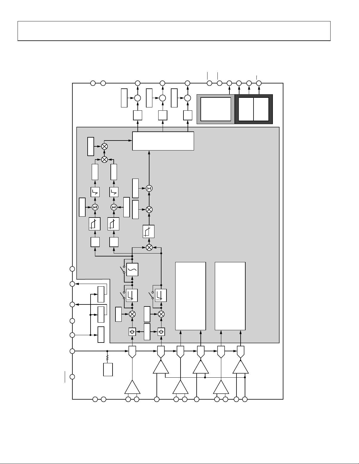
ADE7854/ADE7858/ADE7868/ADE7878
FUNCTIONAL BLOCK DIAGRAMS
PM0
PM1
3
2
CFxDEN
ADE7854
AVAGAIN
AIRMS
AIRMSOS
2
X
AVR MS
LPF
LPF
2
X
08510-204
CF1
33
:
DFC
AWATTOS
AVR MS OS
AWGAIN
CF2
34
:
CFxDEN
DFC
AND
DATA
PHASE C
PHASE A,
PHASE B,
LPF
CF3/HSCLK
35
IRQ0
29
IRQ1
32
SCLK/SCL
MOSI/SDA
MISO/HSD
SS/HSA
39
37
38
36
:
CFxDEN
DFC
C
2
SPI/I
C
2
I
HSDC
PROCESSOR
DIGITAL SIGNAL
VDD AGND AVDD DVDD DGND
IN/OUT
REF
RESET
6
DIGITAL
52426 25174
27
CLKIN
INTEGRATOR
HPF
[23:0]
HPFDIS
AIGAIN
POR LDO LDO
REF
1.2V
28
CLKOUT
7
[23:0]
HPFDIS
ADC
PGA1
8
IAP
IAN
Figure 1. ADE7854 Functional Block Diagram
HPF
AVG AI NAPHCAL
ADC
PGA3
23
VAP
PHASE B
DATA PATH)
ENERGIES AND VOLTAGE/
TOTAL ACTIVE/APPARENT
(SEE PHASE A FOR DETAILED
CURRENT RMS CALCULATI ON FOR
ADC
PGA1
9
IBP
ADC
PGA3
22
12
IBN
VBP
PHASE C
DATA PATH)
ENERGIES AND VOLTAGE/
TOTAL ACTIVE/APPARENT
(SEE PHASE A FOR DETAILED
CURRENT RMS CALCULATI ON FOR
ADC
PGA1
13
ICP
ADC
PGA3
14
19
18
ICN
VN
VCP
Rev. E | Page 4 of 96
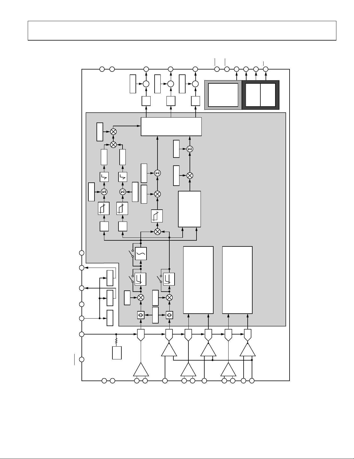
ADE7854/ADE7858/ADE7868/ADE7878
PM0
ADE7858
AIRMSOS
PM1
3
2
AVAGAIN
AIRMS
2
X
AVR MS
LPF
LPF
2
X
CF1
33
:
CF1DEN
DFC
AVR MSO S
AWGAIN AWATTOS
CF2
34
:
CF2DEN
DFC
AND
PHASE C
PHASE A,
PHASE B,
AVARGAIN AVAR OS
LPF
CF3/HSCLK
35
IRQ0
29
IRQ1
32
SCLK/SCL
MOSI/SDA
MISO/HSD
SS/HSA
39
37
38
36
:
CF3DEN
DFC
DATA
TOTAL
BLOCK FOR
COMPUTATI ONAL
REACTIVE PO WER
C
2
SPI/I
C
2
I
HSDC
PROCESSOR
DIGITAL SIGNAL
08510-203
6
DIGITAL
52426 25174
VDD AGND AVDD DVDD DGND
IN/OUT
REF
RESET
27
CLKIN
INTEGRATOR
HPF
[23:0]
HPFDIS
AIGAIN
POR LDO LDO
REF
1.2V
28
CLKOUT
7
[23:0]
HPFDIS
ADC
PGA1
8
IAP
IAN
HPF
APPARENT/ENERG IES AND
14
ICN
DATA PATH)
VOLTAGE/CURRENT
(SEE PHASE A FO R DETAILE D
RMS CALCULATI ON FOR PHASE C
ADC
PGA3
19
18
VN
VCP
DATA PATH)
VOLTAGE/CURRENT
TOTAL ACT IVE/REACT IVE/
AVG AINAPHCAL
ADC
PGA3
23
VAP
APPARENT/ENERG IES AND
(SEE PHASE A FO R DETAILE D
RMS CALCULATI ON FOR PHASE B
ADC
PGA1
9
IBP
ADC
PGA3
22
12
IBN
VBP
TOTAL ACT IVE/REACT IVE/
ADC
PGA1
13
ICP
Figure 2. ADE7858 Functional Block Diagram
Rev. E | Page 5 of 96
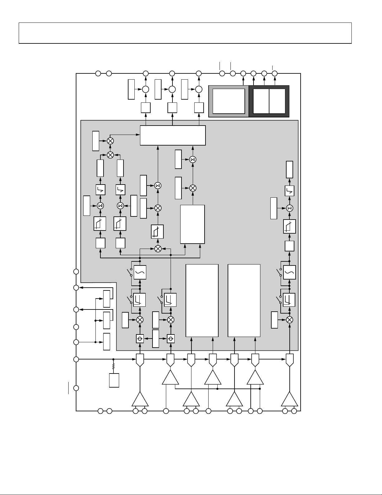
ADE7854/ADE7858/ADE7868/ADE7878
K
IRQ0
IRQ1
SCLK/SCL
MOSI/SDA
MISO/HSD
SS/HSA
39
37
C
2
I
HSDC
PROCESSOR
DIGITAL SIGNAL
ADE7868
AVAGAIN
PM0
PM1
3
2
AIRMS
AVRMS
CF1
33
:
CF1DEN
DFC
CF2
34
:
CF2DEN
DFC
AND
DATA
PHASE C
PHASE A,
PHASE B,
CF3/HSCL
35
32
29
38
36
:
CF3DEN
DFC
C
2
SPI/I
08510-202
NIRMS
AVARGAIN AVAROS
AIRMSOS
LPF
2
X
AVRMSOS
AWGAIN AWATTOS
LPF
LPF
2
X
COMPUTATI ONAL
TOTAL
BLOCK FOR
REACTIVE POW ER
NIRMSOS
LPF
2
X
6
DIGITAL
52426 25174
VDD AGND AVDD DVDD DGND
IN/OUT
INTEGRATOR
HPF
[23:0]
HPFDIS
[23:0]
HPFDIS
AIGAIN
HPF
DATA PATH)
VOLTAGE/CURRENT
TOTAL ACT IVE/REACT IVE/
AVGAINAPHCAL
APPARENT/ENERG IES AND
(SEE PHASE A FO R DETAILE D
RMS CALCULATI ON FOR PHASE B
VOLTAGE/CURRENT
TOTAL ACT IVE/REACT IVE/
APPARENT/ENERG IES AND
RMS CALCULATI ON FOR PHASE C
POR LDO LDO
ADC
ADC
ADC
ADC
ADC
DIGITAL
INTEGRATOR
[23:0]
HPFDIS
DATA PATH)
(SEE PHASE A FO R DETAILE D
ADC
HPF
NIGAIN
ADC
REF
REF
1.2V
PGA3
PGA3
PGA3
RESET
PGA1
7
27
28
CLKIN
CLKOUT
8
IAP
IAN
23
VAP
PGA1
9
IBP
22
12
IBN
VBP
PGA1
13
14
19
18
ICP
ICN
VN
VCP
PGA2
15
16
INP
INN
Figure 3. ADE7868 Functional Block Diagram
Rev. E | Page 6 of 96
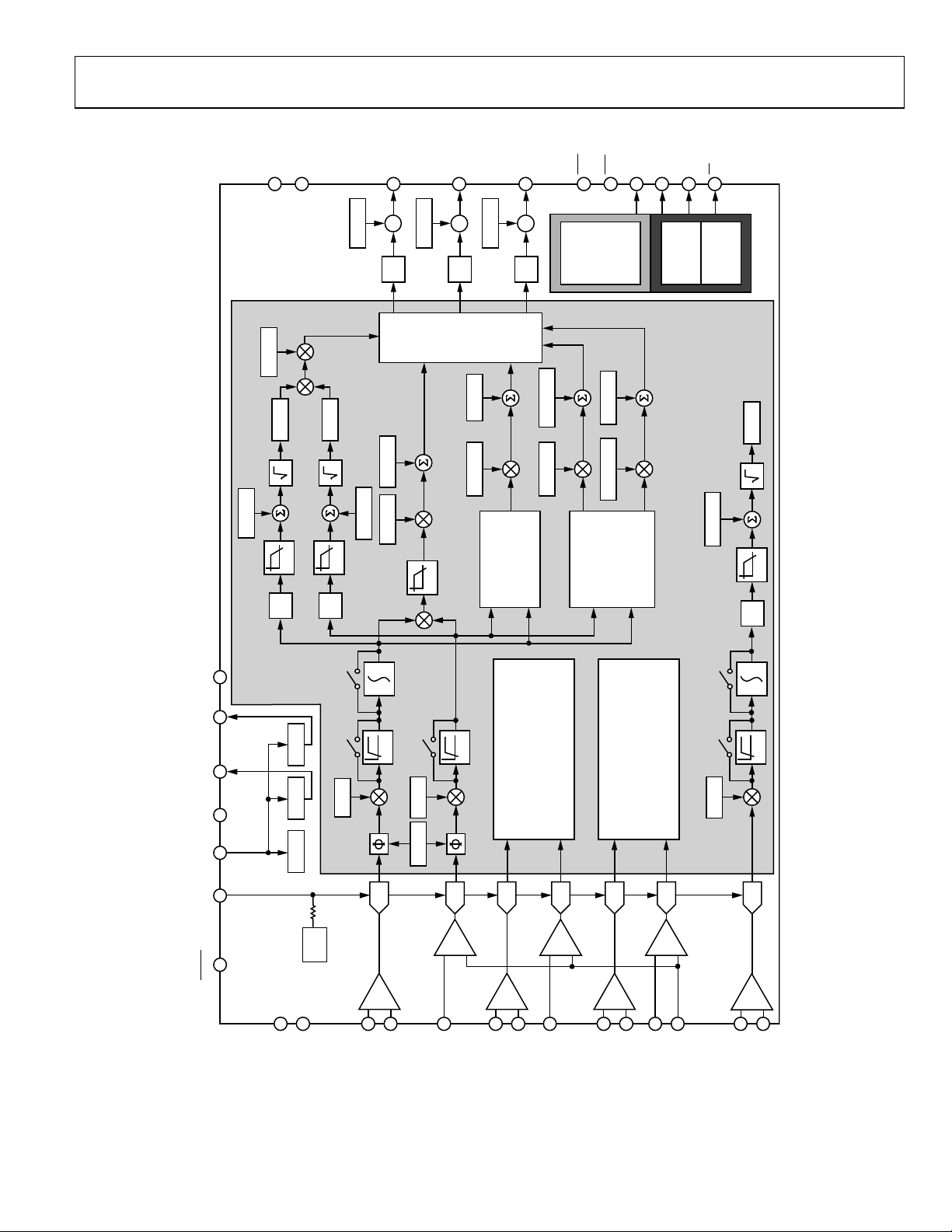
ADE7854/ADE7858/ADE7868/ADE7878
PM0
ADE7878
AIRMSOS
PM1
3
2
AVAGAIN
AIRMS
2
X
AVR MS
LPF
LPF
2
X
CF1
33
:
CF1DEN
DFC
AWATTOS
AVR MSO S
AWGAIN
CF2
34
:
CF2DEN
DFC
AND
PHASE C
PHASE A,
PHASE B,
AVAROS
AVARGAIN
LPF
CF3/HSCLK
35
IRQ0
29
IRQ1
32
SCLK/SCL
MOSI/SDA
MISO/HSD
SS/HSA
39
37
38
36
:
CF3DEN
DFC
DATA
AFWATTO S
AFWGAIN
TOTAL
BLOCK FOR
COMPUT ATIO NAL
REACTIVE PO WER
C
2
SPI/I
AFVARGAIN AFVAROS
BLOCK FOR
ACTIVE AND
FUNDAMENTAL
COMPUTATI ONAL
REACTIVE POWER
C
2
I
HSDC
PROCESSOR
DIGITAL SIGNAL
NIRMSOS
08510-201
NIRMS
LPF
2
X
6
VDD AGND AVDD DVDD DGND
IN/OUT
REF
RESET
DIGITAL
52426 25174
27
CLKIN
INTEGRATOR
HPF
[23:0]
HPFDIS
AIGAIN
POR LDO LDO
REF
1.2V
28
LKOUT
7
[23:0]
HPFDIS
ADC
PGA1
8
IAP
IAN
HPF
DATA PATH)
AVGAINAPHCAL
ADC
PGA3
23
VAP
9
IBP
(SEE PHASE A FOR DET AILED
TOTAL/ FUNDAMENTAL ACTIVE/
REACTIVE ENERGIES, APPARENT
RMS CALCULATI ON FOR PHASE B
ENERGY AND VOL TAGE/CURRENT
ADC
PGA1
ADC
PGA3
22
12
IBN
VBP
TOTAL/ FUNDAMENTAL ACTIVE/
REACTIVE ENERGIES, APPARENT
RMS CALCULATI ON FOR PHASE C
ENERGY AND VOL TAGE/CURRENT
ADC
PGA1
13
14
ICP
ICN
DIGITAL
INTEGRATOR
[23:0]
HPFDIS
DATA PATH)
(SEE PHASE A FOR DET AILED
ADC
PGA3
19
18
VN
VCP
HPF
NIGAIN
ADC
PGA2
15
16
INP
INN
Figure 4. ADE7878 Functional Block Diagram
Rev. E | Page 7 of 96

ADE7854/ADE7858/ADE7868/ADE7878
SPECIFICATIONS
VDD = 3.3 V ± 10%, AGND = DGND = 0 V, on-chip reference, CLKIN = 16.384 MHz, T
MIN
to T
= −40°C to +85°C.
MAX
Table 2.
Parameter
ACCURACY
Active Energy Measurement
0.2 %
AC Power Supply Rejection
Output Frequency Variation 0.01 %
DC Power Supply Rejection VDD = 3.3 V ± 330 mV dc
Output Frequency Variation 0.01 %
Total Active Energy Measurement
REACTIVE ENERGY MEASUREMENT
(ADE7858, ADE7868, AND ADE7878)
Reactive Energy Measurement Error
0.2 %
0.1 %
AC Power Supply Rejection
Output Frequency Variation 0.01 %
1, 2
Min Typ Max Unit Test Conditions/Comments
Active Energy Measurement Error
(per Phase)
Total Active Power 0.1 %
0.1 %
Fundamental Active Power (ADE7878
Only)
0.2 %
0.1 %
Phase Error Between Channels Line frequency = 45 Hz to 65 Hz, HPF on
Power Factor (PF) = 0.8 Capacitive ±0.05 Degrees Phase lead 37°
PF = 0.5 Inductive ±0.05 Degrees Phase lag 60°
Bandwidth
(per Phase)
Total Active Power 0.1 %
0.2 %
0.1 %
Fundamental Active Power (ADE7878
Only)
Phase Error Between Channels Line frequency = 45 Hz to 65 Hz, HPF on
PF = 0.8 Capacitive ±0.05 Degrees Phase lead 37°
PF = 0.5 Inductive ±0.05 Degrees Phase lag 60°
Over a dynamic range of 1000 to 1, PGA = 1, 2, 4;
integrator off
Over a dynamic range of 3000 to 1, PGA = 1, 2, 4;
integrator off
Over a dynamic range of 500 to 1, PGA = 8, 16;
integrator on
0.1 %
2 kHz
0.1 %
Over a dynamic range of 1000 to 1, PGA = 1, 2, 4;
integrator off
Over a dynamic range of 3000 to 1, PGA = 1, 2, 4;
integrator off
Over a dynamic range of 500 to 1, PGA = 8, 16;
integrator on
VDD = 3.3 V + 120 mV rms/120 Hz, IPx = VPx =
±100 mV rms
Over a dynamic range of 1000 to 1, PGA = 1, 2, 4;
integrator off
Over a dynamic range of 3000 to 1, PGA = 1, 2, 4;
integrator off
Over a dynamic range of 500 to 1, PGA = 8, 16;
integrator on
Over a dynamic range of 1000 to 1, PGA = 1, 2, 4;
integrator off
Over a dynamic range of 3000 to 1, PGA = 1, 2, 4;
integrator off
Over a dynamic range of 500 to 1, PGA = 8, 16;
integrator on
VDD = 3.3 V + 120 mV rms/120 Hz, IPx = VPx =
±100 mV rms
Rev. E | Page 8 of 96

ADE7854/ADE7858/ADE7868/ADE7878
Parameter
1, 2
Min Typ Max Unit Test Conditions/Comments
DC Power Supply Rejection VDD = 3.3 V ± 330 mV dc
Output Frequency Variation 0.01 %
Total Reactive Energy Measurement
2 kHz
Bandwidth
RMS MEASUREMENTS
I rms and V rms Measurement
2 kHz
Bandwidth
I rms and V rms Measurement Error
0.1 % Over a dynamic range of 1000 to 1, PGA = 1
(PSM0 Mode)
MEAN ABSOLUTE VALUE (MAV)
MEASUREMENT (ADE7868 AND ADE7878)
I mav Measurement Bandwidth (PSM1
260 Hz
Mode)
I mav Measurement Error (PSM1 Mode) 0.5 % Over a dynamic range of 100 to 1, PGA = 1, 2, 4, 8
ANALOG INPUTS
Maximum Signal Levels ±500 mV peak
Differential inputs between the following pins:
IAP and IAN, IBP and IBN, ICP and ICN; singleended inputs between the following pins: VAP
and VN, VBP and VN, VCP and VN
Input Impedance (DC)
IAP, IAN, IBP, IBN, ICP, ICN, VAP, VBP,
400 kΩ
and VCP Pins
VN Pin 130 kΩ
ADC Offset Error ±2 mV
PGA = 1, uncalibrated error, see the Terminology
section
Gain Error ±4 % External 1.2 V reference
WAVEFORM SAMPLING Sampling CLKIN/2048, 16.384 MHz/2048 = 8 kSPS
Current and Voltage Channels See the Waveform Sampling Mode section
Signal-to-Noise Ratio, SNR 70 dB PGA = 1
Signal-to-Noise-and-Distortion Ratio,
60 dB PGA = 1
SINAD
Bandwidth (−3 dB) 2 kHz
TIME INTERVAL BETWEEN PHASES
Measurement Error 0.3 Degrees Line frequency = 45 Hz to 65 Hz, HPF on
CF1, CF2, CF3 PULSE OUTPUTS
Maximum Output Frequency 8 kHz WTHR = VARTHR = VATHR = PMAX = 33,516,139
Duty Cycle 50 %
If CF1, CF2, or CF3 frequency > 6.25 Hz and
CFDEN is even and > 1
(1 + 1/CFDEN)
× 50%
If CF1, CF2, or CF3 frequency > 6.25 Hz and
CFDEN is odd and > 1
Active Low Pulse Width 80 ms If CF1, CF2, or CF3 frequency < 6.25 Hz
Jitter 0.04 %
For CF1, CF2, or CF3 frequency = 1 Hz and
nominal phase currents are larger than 10% of
full scale
REFERENCE INPUT
REF
Input Voltage Range 1.1 1.3 V Minimum = 1.2 V − 8%; maximum = 1.2 V + 8%
IN/OUT
Input Capacitance 10 pF
ON-CHIP REFERENCE Nominal 1.207 V at the REF
pin at TA = 25°C
IN/OUT
PSM0 and PSM1 Modes
Reference Error ±2 mV
Output Impedance 1.2 kΩ
Temperature Coefficient 10 50 ppm/°C
Maximum value across full temperature range
of −40°C to +85°C
Rev. E | Page 9 of 96

ADE7854/ADE7858/ADE7868/ADE7878
Parameter
1, 2
Min Typ Max Unit Test Conditions/Comments
CLKIN All specifications CLKIN of 16.384 MHz
Input Clock Frequency 16.22 16.384 16.55 MHz
Crystal Equivalent Series Resistance 30 200 Ω
CLKIN Input Capacitance 20 pF
CLKOUT Output Capacitance 20 pF
LOGIC INPUTS—MOSI/SDA, SCLK/SCL, SS,
RESET, PM0, AND PM1
Input High Voltage, V
Input Low Voltage, V
2.0 V VDD = 3.3 V ± 10%
INH
0.8 V VDD = 3.3 V ± 10%
INL
Input Current, IIN −8.7 µA Input = 0 V, VDD = 3.3 V
3 A Input = VDD = 3.3 V
100 nA Input = VDD = 3.3 V
Input Capacitance, CIN 10 pF
LOGIC OUTPUTS—IRQ0, IRQ1, MISO/HSD
VDD = 3.3 V ± 10%
Output High Voltage, VOH 2.4 V VDD = 3.3 V ± 10%
I
800 µA
SOURCE
Output Low Voltage, VOL 0.4 V VDD = 3.3 V ± 10%
I
2 mA
SINK
CF1, CF2, CF3/HSCLK
Output High Voltage, V
I
500 µA
SOURCE
2.4 V VDD = 3.3 V ± 10%
OH
Output Low Voltage, VOL 0.4 V VDD = 3.3 V ± 10%
I
2 mA
SINK
POWER SUPPLY For specified performance
PSM0 Mode
VDD Pin 3.0 3.6 V Minimum = 3.3 V − 10%; maximum = 3.3 V + 10%
IDD 24 26.8 mA
PSM1 and PSM2 Modes (ADE7868 and
ADE7878)
VDD Pin 2.4 3.7 V
IDD
PSM1 Mode 6.0 mA
PSM2 Mode 0.2 mA
PSM3 Mode For specified performance
VDD Pin 2.4 3.7 V
IDD in PSM3 Mode 1.7 A
1
See the Typical Performance Characteristics section.
2
See the Terminology section for a definition of the parameters.
Rev. E | Page 10 of 96
ADE7854/ADE7858/ADE7868/ADE7878
K
TIMING CHARACTERISTICS
VDD = 3.3 V ± 10%, AGND = DGND = 0 V, on-chip reference, CLKIN = 16.384 MHz, T
function pin names are referenced by the relevant function only within the timing tables and diagrams; see the Pin Configuration and
Function Descriptions section for full pin mnemonics and descriptions.
2
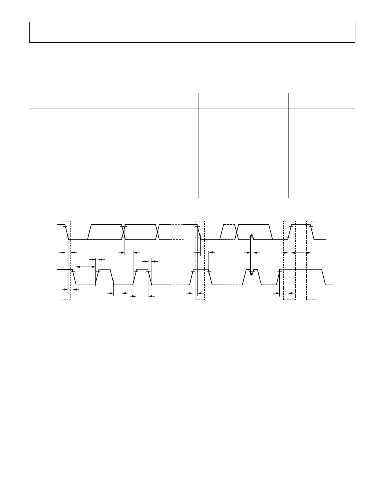
Table 3. I
C-Compatible Interface Timing Parameter
Standard Mode Fast Mode
Parameter Symbol Min Max Min Max Unit
SCL Clock Frequency f
Hold Time (Repeated) Start Condition t
Low Period of SCL Clock t
High Period of SCL Clock t
Set-Up Time for Repeated Start Condition t
Data Hold Time t
Data Setup Time t
0 100 0 400 kHz
SCL
4.0 0.6 s
HD;STA
4.7 1.3 µs
LOW
4.0 0.6 µs
HIGH
4.7 0.6 µs
SU;STA
0 3.45 0 0.9 µs
HD;DAT
250 100 ns
SU;DAT
Rise Time of Both SDA and SCL Signals tR 1000 20 300 ns
Fall Time of Both SDA and SCL Signals tF 300 20 300 ns
Setup Time for Stop Condition t
Bus Free Time Between a Stop and Start Condition t
4.0 0.6 µs
SU;STO
4.7 1.3 µs
BUF
Pulse Width of Suppressed Spikes tSP N/A1 50 ns
1
N/A means not applicable.
MIN
to T
= −40°C to +85°C. Note that dual
MAX
SDA
SCL
START
CONDITIO N
t
F
t
t
LOW
HD;STA
t
HD;DAT
t
STOP
BUF
START
CONDITION
08510-002
t
SU;DAT
t
r
t
HIGH
t
f
Figure 5. I
t
SU;STA
REPEATED START
CONDITIO N
2
C-Compatible Interface Timing
t
HD;STA
t
SP
t
SU;STO
t
r
CONDITIO N
Rev. E | Page 11 of 96
ADE7854/ADE7858/ADE7868/ADE7878
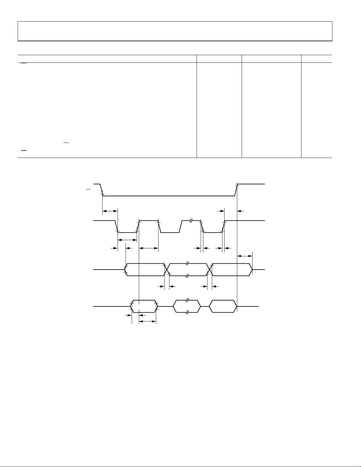
Table 4. SPI Interface Timing Parameters
Parameter Symbol Min Max Unit
t
SS to SCLK Edge
SCLK Period 0.4 4000
SCLK Low Pulse Width tSL 175 ns
SCLK High Pulse Width tSH 175 ns
Data Output Valid After SCLK Edge t
Data Input Setup Time Before SCLK Edge t
Data Input Hold Time After SCLK Edge t
Data Output Fall Time tDF 20 ns
Data Output Rise Time tDR 20 ns
SCLK Rise Time tSR 20 ns
SCLK Fall Time tSF 20 ns
MISO Disable After SS Rising Edge
SS High After SCLK Edge
1
Guaranteed by design.
SS
50 ns
SS
100 ns
DAV
100 ns
DSU
5 ns
DHD
t
200 ns
DIS
t
0 ns
SFS
1
s
SCLK
MISO
MOSI
t
SS
t
SL
t
t
DAV
t
DSU
SH
MSB LSB
MSB IN
t
DHD
INTERMEDIATE BITS
t
DF
INTERMEDIATE BITS
t
SF
t
DR
LSB IN
t
SFS
t
SR
t
DIS
08510-003
Figure 6. SPI Interface Timing
Rev. E | Page 12 of 96
ADE7854/ADE7858/ADE7868/ADE7878
K
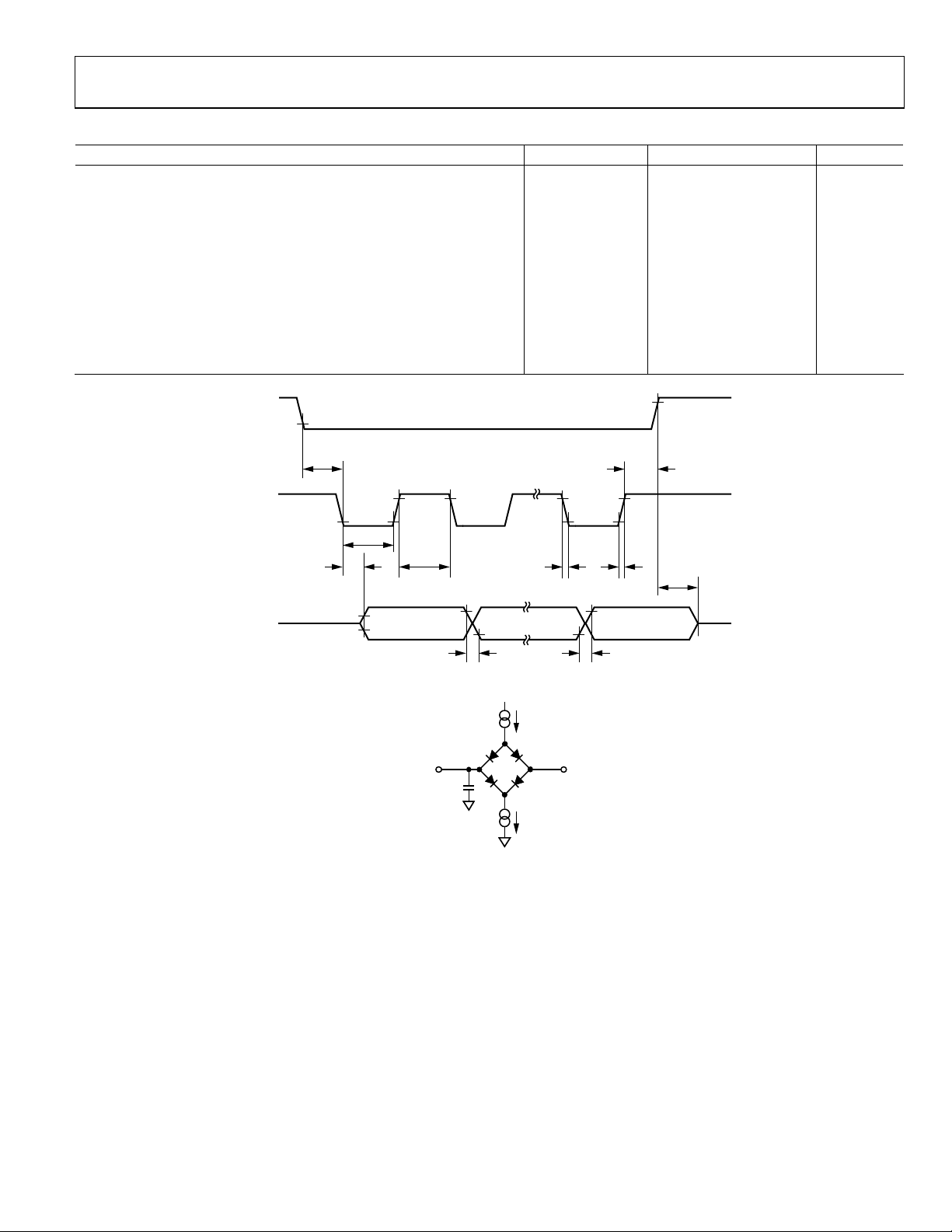
Table 5. HSDC Interface Timing Parameter
Parameter Symbol Min Max Unit
HSA to HSCLK Edge t
HSCLK Period 125 ns
HSCLK Low Pulse Width tSL 50 ns
HSCLK High Pulse Width tSH 50 ns
Data Output Valid After HSCLK Edge t
Data Output Fall Time tDF 20 ns
Data Output Rise Time tDR 20 ns
HSCLK Rise Time tSR 10 ns
HSCLK Fall Time tSF 10 ns
HSD Disable After HSA Rising Edge t
HSA High After HSCLK Edge t
HSA
t
SS
HSCL
t
SL
t
t
DAV
SH
0 ns
SS
40 ns
DAV
5 ns
DIS
0 ns
SFS
t
SFS
t
SF
t
SR
t
DIS
HSD
MSB LSBINTERMEDIATE BITS
t
DF
t
DR
08510-004
Figure 7. HSDC Interface Timing
TO OUTPUT
PIN
50pF
C
2mA I
L
800µA I
OL
1.6V
OH
08510-005
Figure 8. Load Circuit for Timing Specifications
Rev. E | Page 13 of 96
ADE7854/ADE7858/ADE7868/ADE7878
ABSOLUTE MAXIMUM RATINGS
TA = 25°C, unless otherwise noted.
Table 6.
Parameter Rating
VDD to AGND −0.3 V to +3.7 V
VDD to DGND −0.3 V to +3.7 V
Analog Input Voltage to AGND, IAP,
IAN, IBP, IBN, ICP, ICN, VAP, VBP, VCP,
VN
Analog Input Voltage to INP and INN −2 V to +2 V
Reference Input Voltage to AGND −0.3 V to VDD + 0.3 V
Digital Input Voltage to DGND −0.3 V to VDD + 0.3 V
Digital Output Voltage to DGND −0.3 V to VDD + 0.3 V
Operating Temperature
Industrial Range −40°C to +85°C
Storage Temperature Range −65°C to +150°C
Junction Temperature 150°C
Lead Temperature (Soldering, 10 sec) 300°C
Stresses above those listed under Absolute Maximum Ratings
may cause permanent damage to the device. This is a stress
rating only; functional operation of the device at these or any
other conditions above those listed in the operational sections
of this specification is not implied. Exposure to absolute
maximum rating conditions for extended periods may affect
device reliability.
−2 V to +2 V
THERMAL RESISTANCE
θJA is specified equal to 29.3°C/W; θJC is specified equal to
1.8°C/W.
Table 7. Thermal Resistance
Package Type θJA θ
40-Lead LFCSP 29.3 1.8 °C/W
Unit
JC
ESD CAUTION
Rev. E | Page 14 of 96
ADE7854/ADE7858/ADE7868/ADE7878
K
PIN CONFIGURATION AND FUNCTION DESCRIPTIONS
D
K/SCL
F2
CF1
SCL
C
MISO/HS
CF3/HSCL
MOSI/SDA
SS/HSA
NC
37
38
39
40
NC
1
PM0
2
PM1
3
RESET
4
DVDD
5
6
DGND
IAP
7
IAN
8
9
IBP
NC
10
NOTES
1. NC = NO CONNECT .
2. CREATE A SI MILAR PAD ON T HE PCB UNDER THE
EXPOSED PAD. SOL DER THE EXPOSED PAD TO
THE PAD ON THE PCB TO CONFER MECHANICAL
STRENGTH T O THE PACKAGE. DO NOT CO NNECT
THE PADS TO AGND.
ADE78xx
TOP VIEW
(Not to Scale)
11
12
13
14
NC
ICP
IBN
ICN
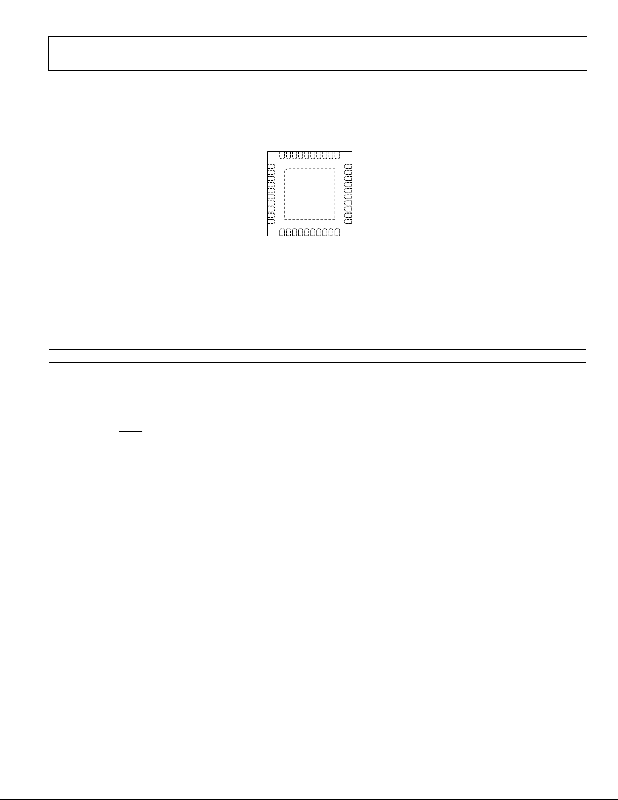
Figure 9. Pin Configuration
Table 8. Pin Function Descriptions
Pin No. Mnemonic Description
1, 10, 11, 20,
NC No Connect. These pins are not connected internally.
21, 30, 31, 40
2 PM0
Power Mode Pin 0. This pin, combined with PM1, defines the power mode of the
ADE7854/ADE7858/ADE7868/ADE7878, as described in Table 9.
3 PM1
Power Mode Pin 1. This pin defines the power mode of the ADE7854/ADE7858/ADE7868/ADE7878
when combined with PM0, as described in Tab le 9.
4
Reset Input, Active Low. In PSM0 mode, this pin should stay low for at least 10 µs to trigger a
RESET
hardware reset.
5 DVDD
This pin provides access to the on-chip 2.5 V digital LDO. Do not connect any external active
circuitry to this pin. Decouple this pin with a 4.7 µF capacitor in parallel with a ceramic 220 nF
capacitor.
6 DGND Ground Reference. This pin provides the ground reference for the digital circuitry.
7, 8 IAP, IAN
Analog Inputs for Current Channel A. This channel is used with the current transducers and is
referenced in this document as Current Channel A. These inputs are fully differential voltage inputs
with a maximum differential level of ±0.5 V. This channel also has an internal PGA equal to the ones
on Channel B and Channel C.
9, 12 IBP, IBN
Analog Inputs for Current Channel B. This channel is used with the current transducers and is
referenced in this document as Current Channel B. These inputs are fully differential voltage inputs
with a maximum differential level of ±0.5 V. This channel also has an internal PGA equal to the ones
on Channel C and Channel A.
13, 14 ICP, ICN
Analog Inputs for Current Channel C. This channel is used with the current transducers and is
referenced in this document as Current Channel C. These inputs are fully differential voltage inputs
with a maximum differential level of ±0.5 V. This channel also has an internal PGA equal to the ones
on Channel A and Channel B.
15, 16 INP, INN
Analog Inputs for Neutral Current Channel N. This channel is used with the current transducers and
is referenced in this document as Current Channel N. These inputs are fully differential voltage
inputs with a maximum differential level of ±0.5 V. This channel also has an internal PGA, different
from the ones found on the A, B, and C channels. The neutral current channel is available in the
ADE7878 and ADE7868. In the ADE7858 and ADE7854, connect these pins to AGND.
17 REF
IN/OUT
This pin provides access to the on-chip voltage reference. The on-chip reference has a nominal
value of 1.2 V. An external reference source with 1.2 V ± 8% can also be connected at this pin. In
either case, decouple this pin to AGND with a 4.7 µF capacitor in parallel with a ceramic 100 nF
capacitor. After reset, the on-chip reference is enabled.
NC
IRQ1
32
31
33
36
34
35
30
NC
29
IRQ0
28
CLKOUT
27
CLKIN
26
VDD
AGND
25
AVDD
24
VAP
23
VBP
22
NC
21
16
18
19
15
INP
20
17
N
VN
NC
IN
VCP
IN/OUT
REF
08510-106
Rev. E | Page 15 of 96

ADE7854/ADE7858/ADE7868/ADE7878
Pin No. Mnemonic Description
18, 19, 22, 23 VN, VCP, VBP, VAP
24 AVDD
25 AGND
26 VDD
27 CLKIN
28 CLKOUT
29, 32
33, 34, 35
36 SCLK/SCL
37 MISO/HSD Data Out for SPI Port/Data Out for HSDC Port.
38 MOSI/SDA Data In for SPI Port/Data Out for I2C Port.
39
EP Exposed Pad
, IRQ1 Interrupt Request Outputs. These are active low logic outputs. See the Interrupts section for a
IRQ0
CF1, CF2,
CF3/HSCLK
/HSA
SS
Analog Inputs for the Voltage Channel. This channel is used with the voltage transducer and is
referenced as the voltage channel in this document. These inputs are single-ended voltage inputs
with a maximum signal level of ±0.5 V with respect to VN for specified operation. This channel also
has an internal PGA.
This pin provides access to the on-chip 2.5 V analog low dropout regulator (LDO). Do not connect
external active circuitry to this pin. Decouple this pin with a 4.7 µF capacitor in parallel with a
ceramic 220 nF capacitor.
Ground Reference. This pin provides the ground reference for the analog circuitry. Tie this pin to the
analog ground plane or to the quietest ground reference in the system. Use this quiet ground
reference for all analog circuitry, for example, antialiasing filters, current, and voltage transducers.
Supply Voltage. This pin provides the supply voltage. In PSM0 (normal power mode), maintain the
supply voltage at 3.3 V ± 10% for specified operation. In PSM1 (reduced power mode), PSM2 (low
power mode), and PSM3 (sleep mode), when the ADE7868/ADE7878 is supplied from a battery,
maintain the supply voltage between 2.4 V and 3.7 V. Decouple this pin to AGND with a 10 µF
capacitor in parallel with a ceramic 100 nF capacitor. The only modes available on the ADE7858 and
ADE7854 are the PSM0 and PSM3 power modes.
Master Clock. An external clock can be provided at this logic input. Alternatively, a parallel resonant
AT-cut crystal can be connected across CLKIN and CLKOUT to provide a clock source for the
ADE7854/ADE7858/ADE7868/ADE7878. The clock frequency for specified operation is 16.384 MHz.
Use ceramic load capacitors of a few tens of picofarad with the gate oscillator circuit. Refer to the
crystal manufacturer’s data sheet for load capacitance requirements.
A crystal can be connected across this pin and CLKIN (as previously described with Pin 27 in this
table) to provide a clock source for the ADE7854/ADE7858/ADE7868/ADE7878. The CLKOUT pin can
drive one CMOS load when either an external clock is supplied at CLKIN or a crystal is being used.
detailed presentation of the events that can trigger interrupts.
Calibration Frequency (CF) Logic Outputs. These outputs provide power information based on the
CF1SEL[2:0], CF2SEL[2:0], and CF3SEL[2:0] bits in the CFMODE register. These outputs are used for
operational and calibration purposes. The full-scale output frequency can be scaled by writing to the
CF1DEN, CF2DEN, and CF3DEN registers, respectively (see the Energy-to-Frequency Conversion
section). CF3 is multiplexed with the serial clock output of the HSDC port.
Serial Clock Input for SPI Port/Serial Clock Input for I
to this clock (see the Serial Interfaces section). This pin has a Schmidt trigger input for use with a
clock source that has a slow edge transition time, for example, opto-isolator outputs.
Slave Select for SPI Port/HSDC Port Active.
Create a similar pad on the PCB under the exposed pad. Solder the exposed pad to the pad on the
PCB to confer mechanical strength to the package. Do not connect the pads to AGND.
2
C Port. All serial data transfers are synchronized
Rev. E | Page 16 of 96
ADE7854/ADE7858/ADE7868/ADE7878
TYPICAL PERFORMANCE CHARACTERISTICS
0.10
0.05
0
–0.05
–0.10
–0.15
–0.20
ERROR (%)
–0.25
–0.30
–0.35
–0.40
0.01 0.1 1 10
PERCENTAGE OF F ULL-SCALE CURRENT (%)
+85°C, PO WER FACTO R = 1.0
+25°C, PO WER FACTO R = 1.0
–40°C, POWER FACTO R = 1.0
100
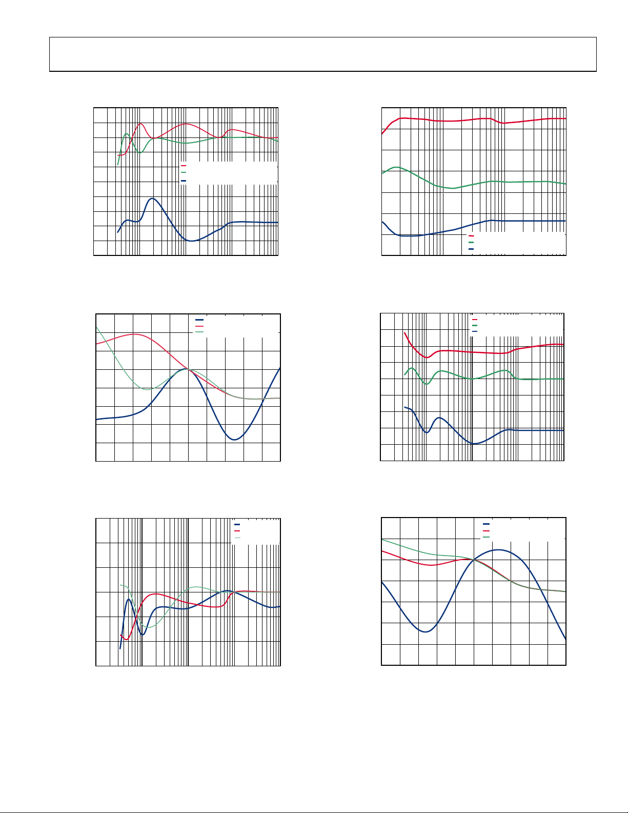
Figure 10. Total Active Energy Error As Percentage of Reading (Gain = +1,
Power Factor = 1) over Temperature with Internal Reference and Integrator Off
0.15
0.10
0.05
0
–0.05
ERROR (%)
–0.10
–0.15
–0.20
–0.25
45 47 49 51 53 55 57 59 61 63 65
LINE FREQUENCY (Hz)
POWER FACTOR = 1
POWER FACTOR = +0.5
POWER FACTOR = –0.5
08510-305
Figure 11. Total Active Energy Error As Percentage of Reading (Gain = +1)
over Frequency with Internal Reference and Integrator Off
0.15
0.10
0.05
0
ERROR (%)
–0.05
VDD = 2.97V
V
= 3.30V
DD
V
= 3.63V
DD
8510-301
0.50
0.40
0.30
0.20
0.10
0
ERROR (%)
–0.10
–0.20
–0.30
–0.40
–0.50
0.001 0.01 0.1 1
PERCENTAGE OF F ULL-SCALE CURRENT (%)
+85°C, POW ER FACTOR = 1.0
+25°C, POW ER FACTOR = 1.0
–40°C, POW ER FACTOR = 1.0
08510-308
Figure 13. Total Active Energy Error As Percentage of Reading (Gain = +16,
Powe r Fact or = 1) over Temperature wit h Internal Reference and Integrator On
0.40
0.30
0.20
0.10
0
–0.10
ERROR (%)
–0.20
–0.30
–0.40
–0.50
0.01 0.1 1 10 100
PERCENTAGE OF F ULL-SCALE CURRENT (%)
+85°C, PO WER FACTO R = 0
+25°C, PO WER FACTO R = 0
–40°C, POW ER FACTOR = 0
08510-311
Figure 14. Total Reactive Energy Error As Percentage of Reading (Gain = +1,
Power Factor = 0) over Temperature with Internal Reference and Integrator Off
ERROR (%)
0.10
0.05
0
–0.05
–0.10
–0.15
POWER FACTOR = 0
POWER FACTOR = +0.5
POWER FACTOR = –0.5
–0.10
–0.15
0.01 0.1 1 10 100
PERCENTAGE OF F ULL-SCALE CURRENT (%)
08510-306
Figure 12. Total Active Energy Error As Percentage of Reading (Gain = +1,
Power Factor = 1) over Power Supply with Internal Reference and Integrator Off
Rev. E | Page 17 of 96
–0.20
–0.25
45 47 49 51 53 55 57 59 61 63 65
LINE FREQ UENCY (Hz)
08510-315
Figure 15. Total Reactive Energy Error As Percentage of Reading (Gain = +1)
over Frequency with Internal Reference and Integrator Off
ADE7854/ADE7858/ADE7868/ADE7878
0.30
0.20
0.10
0
ERROR (%)
–0.10
–0.20
–0.30
0.01 0.1 1 10 10 0
PERCENTAGE OF F ULL-SCALE CURRENT (%)
VDD = 2.97V
V
= 3.30V
DD
V
= 3.63V
DD
08510-316
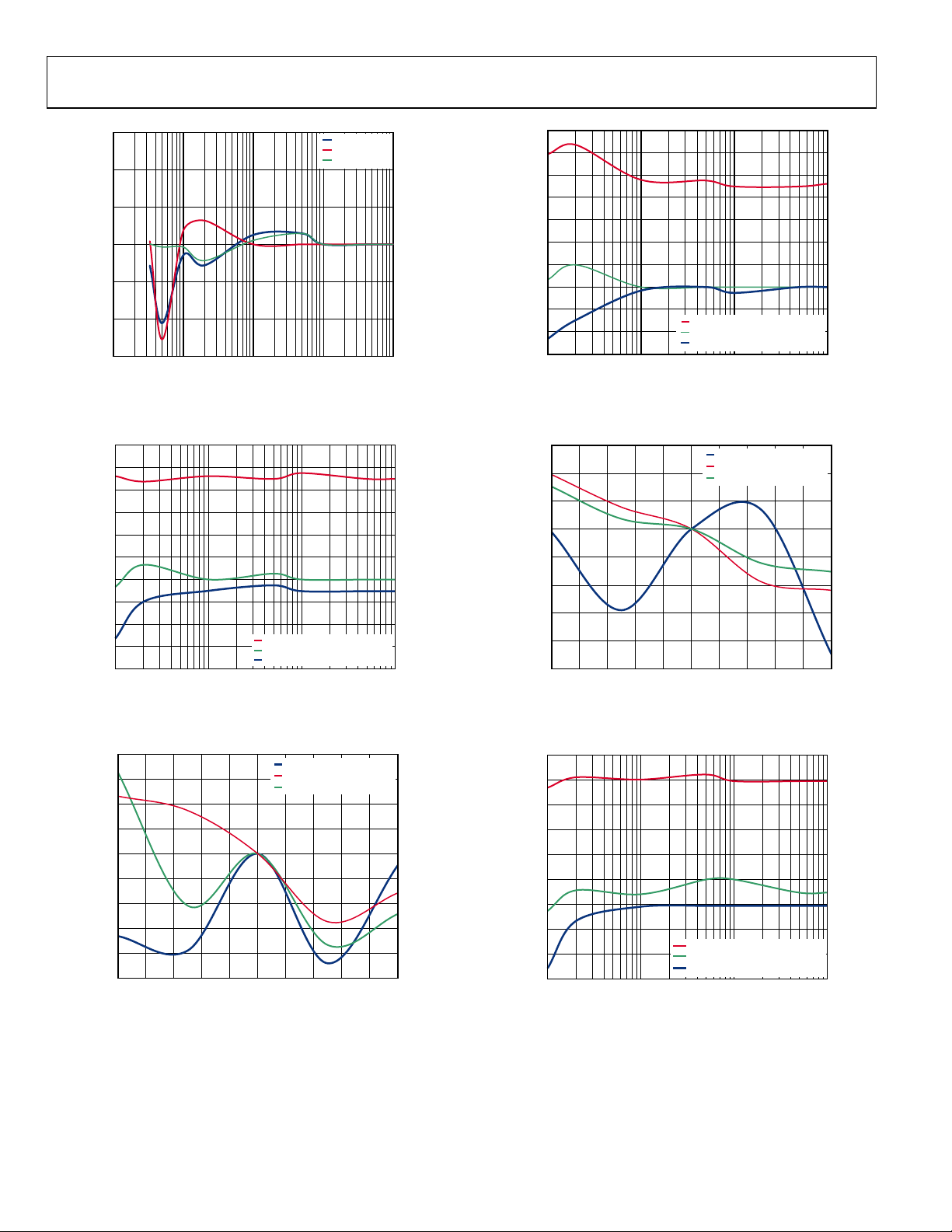
Figure 16. Total Reactive Energy Error As Percentage of Reading (Gain = +1,
Powe r Fact or = 0) over Power Supply with Internal Reference and Integrator Off
0.60
0.50
0.40
0.30
0.20
0.10
ERROR (%)
0
–0.10
–0.20
–0.30
–0.40
0.1 1 10 100
PERCENTAGE OF F ULL-SCALE CURRENT (%)
+85°C, POWER FACTO R = 0
+25°C, POWER FACTO R = 0
–40°C, POW ER FACTOR = 0
08510-318
Figure 17. Total Reactive Energy Error As Percentage of Reading (Gain = +16,
Powe r Fact or = 1) over Temperature with Internal Reference and Integrator On
0.20
0.15
0.10
0.05
0
–0.05
ERROR (%)
–0.10
–0.15
–0.20
–0.25
45 47 49 51 53 55 57 59 61 63 65
LINE FREQUENCY (Hz)
POWER FACTOR = 1.0
POWER FACT OR = +0.5
POWER FACTOR = –0.5
8510-335
Figure 18. Fundamental Active Energy Error As Percentage of Reading
(Gain = +1) over Frequency with Internal Reference and Integrator Off
0.70
0.60
0.50
0.40
0.30
0.20
0.10
ERROR (%)
0
–0.10
–0.20
–0.30
0.1 1 10 100
PERCENTAGE OF FUL L-SCALE CURRENT (%)
+85°C, PO WER FACTOR = 1.0
+25°C, POW ER FACTOR = 1.0
–40°C, POW ER FACTOR = 1.0
Figure 19. Fundamental Active Energy Error As Percentage of Reading
(Gain = +16) over Temperature with Internal Reference and Integrator On
0.15
0.10
0.05
0
–0.05
ERROR (%)
–0.10
–0.15
–0.20
–0.25
45 47 49 51 53 55 57 59 61 63 65
LINE FREQUENCY (Hz)
POWER FACTOR = 1.0
POWER FACTOR = +0.5
POWER FACTOR = –0.5
08510-345
Figure 20. Fundamental Reactive Energy Error As Percentage of Reading
(Gain = +1) over Frequency with Internal Reference and Integrator Off
0.50
0.40
0.30
0.20
0.10
0
ERROR (%)
–0.10
–0.20
–0.30
–0.40
0.1 1 10 100
PERCENTAGE OF F ULL-SCALE CURRENT (%)
+85°C, PO WER FACTOR = 1.0
+25°C, PO WER FACTOR = 1.0
–40°C, POW ER FACTOR = 1.0
Figure 21. Fundamental Reactive Energy Error As Percentage of Reading
(Gain = +16) over Temperature with Internal Reference and Integrator On
08510-338
08510-348
Rev. E | Page 18 of 96
ADE7854/ADE7858/ADE7868/ADE7878
V
TEST CIRCUIT
1kΩ
1kΩ
1kΩ
1kΩ
18nF
18nF
10kΩ
18nF
18nF
3.3V
SAME AS
IAP, IAN
SAME AS
IAP, IAN
SAME AS
VCP
SAME AS
VCP
+ +
4
7
8
9
12
13
14
18
19
22
23
2
3
0.22µF
PM0
PM1
RESET
IAP
IAN
IBP
IBN
ICP
ICN
VN
VCP
VBP
VAP
4.7µF
1µF
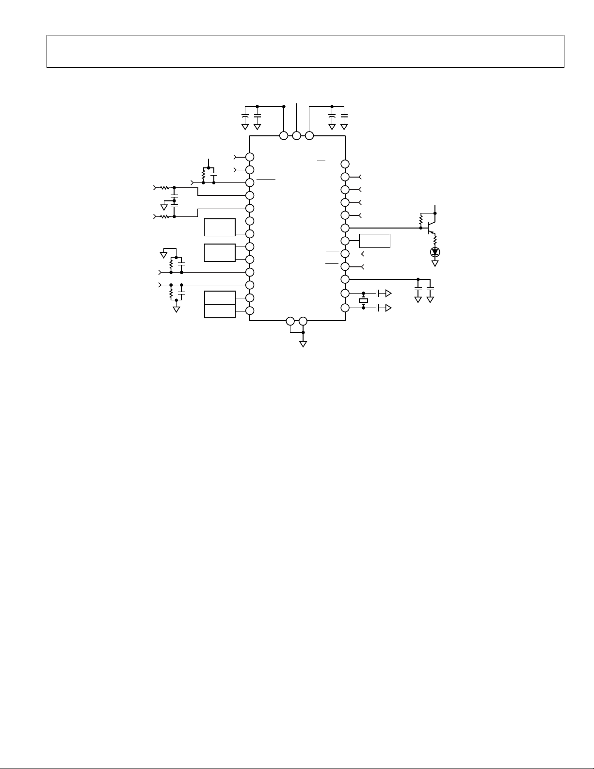
Figure 22. Test Circuit
3.3
26
24
VDD
AVDD
ADE78xx
AGND
DGND
25
6
4.7µF
5
DVDD
SS/HSA
MOSI/SDA
MISO/HSD
SCLK/SCL
CF3/HSCLK
CF2
CF1
IRQ1
IRQ0
REF
IN/OUT
CLKOUT
CLKIN
39
38
37
36
35
34
33
32
29
17
28
27
0.22µF
SAME AS
CF2
20pF
16.384MHz
20pF
10kΩ
4.7µF
3.3V
1.5kΩ
+
0.1µF
08510-099
Rev. E | Page 19 of 96

ADE7854/ADE7858/ADE7868/ADE7878
+
−
TERMINOLOGY
Measurement Error
The error associated with the energy measurement made by the
ADE7854/ADE7858/ADE7868/ADE7878 is defined by
Measurement Error =
7878×−
EnergyTrue
EnergyTrueADEbyRegisteredEnergy
(1)
%100
Phase Error Between Channels
The high-pass filter (HPF) and digital integrator introduce a
slight phase mismatch between the current and the voltage
channel. The all digital design ensures that the phase matching
between the current channels and voltage channels in all three
phases is within ±0.1° over a range of 45 Hz to 65 Hz and ±0.2°
over a range of 40 Hz to 1 kHz. This internal phase mismatch
can be combined with the external phase error (from current
sensor or component tolerance) and calibrated with the phase
calibration registers.
Power Supply Rejection (PSR)
This quantifies the ADE7878 measurement error as a percentage of reading when the power supplies are varied. For the ac
PSR measurement, a reading at nominal supplies (3.3 V) is
taken. A second reading is obtained with the same input signal
levels when an ac signal (120 mV rms at 100 Hz) is introduced
onto the supplies. Any error introduced by this ac signal is
expressed as a percentage of reading—see the Measurement
Error definition.
For the dc PSR measurement, a reading at nominal supplies
(3.3 V) is taken. A second reading is obtained with the same
input signal levels when the power supplies are varied ±10%.
Any error introduced is expressed as a percentage of the
reading.
ADC Offset Error
This refers to the dc offset associated with the analog inputs to
the ADCs. It means that with the analog inputs connected to
AGND, the ADCs still see a dc analog input signal. The magnitude of the offset depends on the gain and input range selection
(see the Typical Performance Characteristics section). However,
the HPF removes the offset from the current and voltage channels
and the power calculation remains unaffected by this offset.
Gain Error
The gain error in the ADCs of the ADE7858/ADE7868/ADE7878/
ADE7854 is defined as the difference between the measured
ADC output code (minus the offset) and the ideal output code
(see the Current Channel ADC section and the Voltage Channel
ADC section). The difference is expressed as a percentage of the
ideal code.
CF Jitter
The period of pulses at one of the CF1, CF2, or CF3 pins is
continuously measured. The maximum, minimum, and average
values of four consecutive pulses are computed as follows:
Maximum = max(Period
Minimum = min(Period
Average =
, Period1, Period2, Period3)
0
, Period1, Period2, Period3)
0
PeriodPeriodPeriodPeriod ++
4
3210
The CF jitter is then computed as
CF
JITTER
=
MinimumMaximum
Average
%100×
(2)
Rev. E | Page 20 of 96

ADE7854/ADE7858/ADE7868/ADE7878
POWER MANAGEMENT
The ADE7868/ADE7878 have four modes of operation, determined by the state of the PM0 and PM1 pins (see Tab le 9 ). The
ADE7854/ADE7858 have two modes of operation. These pins
provide complete control of the ADE7854/ADE7858/ADE7868/
ADE7878 operation and can easily be connected to an external
microprocessor I/O. The PM0 and PM1 pins have internal pullup resistors. See Ta ble 11 and Tabl e 12 for a list of actions that are
recommended before and after setting a new power mode.
Table 9. Power Supply Modes
Power Supply Modes PM1 PM0
PSM0, Normal Power Mode 0 1
PSM1, Reduced Power Mode1 0 0
PSM2, Low Power Mode1 1 0
PSM3, Sleep Mode 1 1
1
Available in the ADE7868 and ADE7878.
PSM0—NORMAL POWER MODE (ALL PARTS)
In PSM0 mode, the ADE7854/ADE7858/ADE7868/ADE7878
are fully functional. The PM0 pin is set to high and the PM1 pin
is set to low for the ADE78xx to enter this mode. If the ADE78xx
is in one of PSM1, PSM2, or PSM3 modes and is switched into
PSM0 mode, then all control registers take the default values with
the exception of the threshold register, LPOILVL, which is used
in PSM2 mode, and the CONFIG2 register, both of which
maintain their values.
The ADE7854/ADE7858/ADE7868/ADE7878 signal the end of
IRQ1
the transition period by triggering the
setting Bit 15 (RSTDONE) in the STATUS1 register to 1. This bit is
0 during the transition period and becomes 1 when the transition is
finished. The status bit is cleared and the
high by writing to the STATUS1 register with the corresponding
bit set to 1. Bit 15 (RSTDONE) in the interrupt mask register
does not have any functionality attached even if the
low when Bit 15 (RSTDONE) in the STATUS1 register is set to 1.
This makes the RSTDONE interrupt unmaskable.
interrupt pin low and
IRQ1
pin is set back to
IRQ1
pin goes
PSM1—REDUCED POWER MODE (ADE7868, ADE7878 ONLY)
The reduced power mode, PSM1, is available on the ADE7868
and ADE7878 only. In this mode, the ADE7868/ADE7878
measure the mean absolute values (mav) of the 3-phase currents
and store the results in the AIMAV, BIMAV, and CIMAV 20-bit
registers. This mode is useful in missing neutral cases in which
the voltage supply of the ADE7868 or ADE7878 is provided by an
external battery. The serial ports, I
mode; the active port can be used to read the AIMAV, BIMAV,
and CIMAV registers. It is not recommended to read any of the
other registers because their values are not guaranteed in this
mode. Similarly, a write operation is not taken into account by
the ADE7868/ADE7878 in this mode.
2
C or SPI, are enabled in this
In summary, in this mode, it is not recommended to access any
register other than AIMAV, BIMAV, and CIMAV. The circuit
that measures these estimates of rms values is also active during
PSM0; therefore, its calibration can be completed in either PSM0
mode or in PSM1 mode. Note that the ADE7868 and ADE7878
do not provide any register to store or process the corrections
resulting from the calibration process. The external microprocessor
stores the gain values in connection with these measurements
and uses them during PSM1 (see the Current Mean Absolute
Value Calculation—ADE7868 and ADE7878 Only section for
more details on the xIMAV registers).
The 20-bit mean absolute value measurements done in PSM1,
although available also in PSM0, are different from the rms
measurements of phase currents and voltages executed only in
PSM0 and stored in the xIRMS and xVRMS 24-bit registers. See
the Current Mean Absolute Value Calculation—ADE7868 and
ADE7878 Only section for details.
If the ADE7868/ADE7878 is set in PSM1 mode while still in the
PSM0 mode, the ADE7868/ADE7878 immediately begin the
mean absolute value calculations without any delay. The xIMAV
registers are accessible at any time; however, if the ADE7878 or
ADE7868 is set in PSM1 mode while still in PSM2 or PSM3
modes, the ADE7868/ADE7878 signal the start of the mean
IRQ1
absolute value computations by triggering the
The xIMAV registers can be accessed only after this moment.
pin low.
PSM2—LOW POWER MODE (ADE7868, ADE7878 ONLY)
The low power mode, PSM2, is available on the ADE7868 and
ADE7878 only. In this mode, the ADE7868/ADE7878 compare
all phase currents against a threshold for a period of 0.02 ×
(LPLINE[4:0] + 1) seconds, independent of the line frequency.
LPLINE[4:0] are Bits[7:3] of the LPOILVL register (see Tabl e 1 0).
Table 10. LPOILVL Register
Bit Mnemonic Default Description
[2:0] LPOIL[2:0] 111
[7:3] LPLINE[4:0] 00000
The threshold is derived from Bits[2:0] (LPOIL[2:0]) of the
LPOILVL register as LPOIL[2:0]/8 of full scale. Every time
one phase current becomes greater than the threshold, a
counter is incremented. If every phase counter remains below
LPLINE[4:0] + 1 at the end of the measurement period, then
IRQ0
the
greater or equal to LPLINE[4:0] + 1 at the end of the measurement period, the
how the ADE7868/ADE7878 behave in PSM2 mode when
pin is triggered low. If a single phase counter becomes
IRQ1
pin is triggered low. illustrates
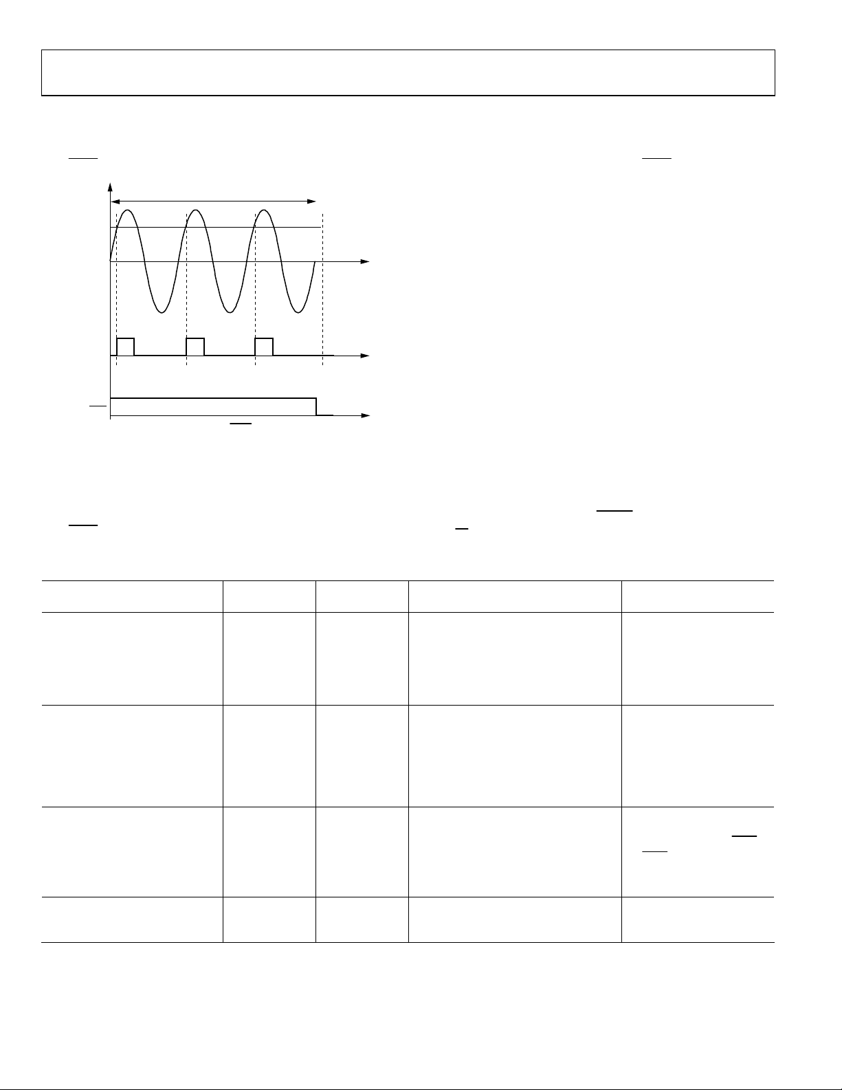
Threshold is put at a value
corresponding to full scale
multiplied by LPOIL/8.
The measurement period is
(LPLINE[4:0] + 1)/50 sec.
Figure 23
Rev. E | Page 21 of 96
ADE7854/ADE7858/ADE7868/ADE7878
T
LPLINE[4:0] = 2 and LPOIL[2:0] = 3. The test period is three
50 Hz cycles (60 ms), and the Phase A current rises above the
LPOIL[2:0] threshold three times. At the end of the test period,
IRQ1
the
pin is triggered low.
IA CURREN
PHASE
COUNTER = 1
IRQ1
Figure 23. PSM2 Mode Triggering
LPLINE[4:0] = 2
PHASE
COUNTER = 2
IRQ1
(50 Hz Systems)
LPOIL [2:0]
THRESHOLD
PHASE
COUNTER = 3
Pin for LPLINE[4:0] = 2
The I2C or SPI port is not functional during this mode. The PSM2
mode reduces the power consumption required to monitor the
currents when there is no voltage input and the voltage supply
of the ADE7868/ADE7878 is provided by an external battery. If
IRQ0
the
pin is triggered low at the end of a measurement period,
08510-008
this signifies all phase currents stayed below threshold and,
therefore, there is no current flowing through the system.
At this point, the external microprocessor sets the ADE7868/
IRQ1
ADE7878 into Sleep Mode PSM3. If the
pin is triggered
low at the end of the measurement period, this signifies that at
least one current input is above the defined threshold and
current is flowing through the system, although no voltage is
present at the ADE7868/ADE7878 pins. This situation is often
called missing neutral and is considered a tampering situation,
at which point the external microprocessor sets the ADE7868/
ADE7878 into PSM1 mode, measures the mean absolute values
of phase currents, and integrates the energy based on their values
and the nominal voltage.
It is recommended to use the ADE7868/ADE7878 in PSM2
mode when Bits[2:0] (PGA1[2:0]) of the gain register are equal
to 1 or 2. These bits represent the gain in the current channel
datapath. It is not recommended to use the ADE7868/ADE7878
in PSM2 mode when the PGA1[2:0] bits are equal to 4, 8, or 16.
PSM3—SLEEP MODE (ALL PARTS)
The sleep mode is available on all parts (ADE7854, ADE7858,
ADE7868, and ADE7878). In this mode, the ADE78xx has most
of its internal circuits turned off and the current consumption is
at its lowest level. The I
tional during this mode, and the
SS
and
/HSA pins should be set high.
2
C, HSDC, and SPI ports are not func-
RESET
, SCLK/SCL, MOSI/SDA,
Table 11. Power Modes and Related Characteristics
LPOILVL,
Power Mode All Registers1
CONFIG2 I2C/SPI Functionality
PSM0
State After Hardware Reset Set to default Set to default I2C enabled
All circuits are active and
DSP is in idle mode.
State After Software Reset Set to default Unchanged
Active serial port is unchanged if lockin procedure has been previously
All circuits are active and
DSP is in idle mode.
executed
PSM1—ADE7878, ADE7868 Only
Not available
Values set
during PSM0
unchanged
Enabled
Current mean absolute
values are computed and
the results are stored in
the AIMAV, BIMAV, and
CIMAV registers. The I
SPI serial port is enabled
with limited functionality.
PSM2—ADE7878, ADE7868 Only Not available
Values set
during PSM0
unchanged
Disabled
Compares phase currents
against the threshold set
in LPOILVL. Triggers IRQ0
or IRQ1 pins accordingly.
The serial ports are not
available.
PSM3 Not available
Values set
during PSM0
unchanged
1
Setting for all registers except the LPOILVL and CONFIG2 registers.
Disabled
Internal circuits shut down
and the serial ports are
not available.
2
C or
Rev. E | Page 22 of 96

ADE7854/ADE7858/ADE7868/ADE7878
Table 12. Recommended Actions When Changing Power Modes
Initial Power
Mode
PSM0
PSM1—
ADE7878,
ADE7868 Only
PSM2—
ADE7878,
ADE7868 Only
PSM3 No action necessary.
Recommended Actions
Before Setting Next
Power Mode
Stop DSP by setting the run
register = 0x0000.
Disable HSDC by clearing
Bit 6 (HSDEN) to 0 in the
CONFIG register.
Mask interrupts by setting
MASK0 = 0x0 and
MASK1 = 0x0.
Erase interrupt status flags
in the STATUS0 and STATUS1
registers.
No action necessary.
No action necessary.
PSM0 PSM1 PSM2 PSM3
Wait until the IRQ1 pin
is triggered low.
Poll the STATUS1
register until Bit 15
(RSTDONE) is set to 1.
Wait until the IRQ1 pin
is triggered low.
Poll the STATUS1
register until Bit 15
(RSTDONE) is set to 1.
Wait until the IRQ1 pin
is triggered low.
Poll the STATUS1
register until Bit 15
(RSTDONE) is set to 1.
Current mean absolute
values (mav) computed
immediately.
xIMAV registers can be
accessed immediately.
Wait until the IRQ1 pin
triggered low.
Current mean absolute
values compute at this
moment.
xIMAV registers may be
accessed from this
moment.
Wait until the IRQ1 pin is
triggered low.
Current mav circuit
begins computations at
this time.
xIMAV registers can be
accessed from this
moment.
Next Power Mode
Wait until the IRQ0
pin is
or IRQ1
triggered
accordingly.
Wait until the IRQ0
pin is
or IRQ1
triggered
accordingly.
Wait until the IRQ0
pin is
or IRQ1
triggered
accordingly.
No action
necessary.
No action
necessary.
No action
necessary.
Rev. E | Page 23 of 96
ADE7854/ADE7858/ADE7868/ADE7878
POWER-UP PROCEDURE
3.3V – 10%
2.0V ± 10%
0V
ADE78xx
POWERED UP
POR TIMER
TURNED ON
ADE78xx
ENTER PSM3
Figure 24. Power-Up Procedure
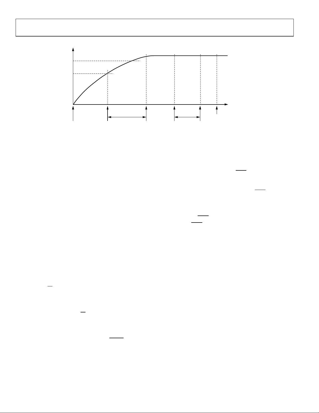
The ADE7854/ADE7858/ADE7868/ADE7878 contain an onchip power supply monitor that supervises the power supply
(VDD). At power-up, until VDD reaches 2 V ± 10%, the chip is
in an inactive state. As VDD crosses this threshold, the power
supply monitor keeps the chip in this inactive state for an
additional 26 ms, allowing VDD to achieve 3.3 V − 10%, the
minimum recommended supply voltage. Because the PM0 and
PM1 pins have internal pull-up resistors and the external microprocessor keeps them high, the ADE7854/ADE7858/ADE7868/
ADE7878 always power-up in sleep mode (PSM3). Then, an
external circuit (that is, a microprocessor) sets the PM1 pin to a
low level, allowing the ADE78xx to enter normal mode (PSM0).
The passage from PSM3 mode, in which most of the internal
circuitry is turned off, to PSM0 mode, in which all functionality
is enabled, is accomplished in less than 40 ms (see Figure 24 for
details).
If PSM0 mode is the only desired power mode, the PM1 pin can
be set low permanently by using a direct connection to ground.
The PM0 pin can remain open because the internal pull-up
resistor ensures that its state is high.
When the ADE7854/ADE7858/ADE7868/ADE7878 enter PSM0
2
mode, the I
used, then the
low. This action selects the SPI port for further use. If I
C port is the active serial port. If the SPI port is
SS
/HSA pin must be toggled three times, high to
2
C is the
active serial port, Bit 1 (I2C_LOCK) of the CONFIG2 register
must be set to 1 to lock it in. From this moment, the ADE78xx
SS
ignores spurious toggling of the
/HSA pin, and an eventual
switch to use the SPI port is no longer possible. Likewise, if SPI
is the active serial port, any write to the CONFIG2 register locks
2
the port, at which time a switch to use the I
possible. Only a power-down or by setting the
C port is no longer
RESET
pin low
can the ADE7854/ADE7858/ADE7868/ADE7878 be reset to use
2
the I
C port. Once locked, the serial port choice is maintained
when the ADE78xx changes PSMx power modes.
Rev. E | Page 24 of 96
ADE78xx
PSM0 READY
40ms26ms
MICROPROCESSOR
SETS ADE78xx
IN PSM0
RSTDONE
INTERRUPT
TRIGGERED
MICROPROCESSOR
MAKES THE
CHOICE BETWE EN
2
C AND SPI
I
08510-009
Immediately after entering PSM0, the ADE7854/ADE7858/
ADE7868/ADE7878 set all registers to their default values,
including the CONFIG2 and LPOILVL registers.
The ADE7854/ADE7858/ADE7868/ADE7878 signals the end of
IRQ1
the transition period by triggering the
interrupt pin low and
setting Bit 15 (RSTDONE) in the STATUS1 register to 1. This
bit is 0 during the transition period and becomes 1 when the
IRQ1
transition ends. The status bit is cleared and the
pin is
returned high by writing the STATUS1 register with the corresponding bit set to 1. Because the RSTDONE is an unmaskable
interrupt, Bit 15 (RSTDONE) in the STATUS1 register must be
IRQ1
cancelled for the
wait until the
IRQ1
pin to return high. It is recommended to
pin goes low before accessing the STATUS1
register to test the state of the RSTDONE bit. At this point, as a
good programming practice, it is also recommended to cancel
all other status flags in the STATUS1 and STATUS0 registers by
writing the corresponding bits with 1.
Initially, the DSP is in idle mode, which means it does not
execute any instruction. This is the moment to initialize all
ADE78xx registers. The last register in the queue must be
written three times to ensure the register has been initialized.
Then, enable the data memory RAM protection and write
0x0001 into the run register to start the DSP (see the Digital
Signal Processor section for details on data memory RAM
protection and the run register).
If the supply voltage, VDD, drops lower than 2 V ± 10%, the
ADE7854/ADE7858/ADE7868/ADE7878 enter an inactive state,
which means that no measurements or computations are executed.

ADE7854/ADE7858/ADE7868/ADE7878
HARDWARE RESET
The ADE7854/ADE7858/ADE7868/ADE7878 each has a
RESET
pin. If the ADE7854, ADE7858, ADE7868, or ADE7878
is in PSM0 mode and the
ADE78xx enters the hardware reset state. The ADE78xx must
be in PSM0 mode for a hardware reset to be considered. Setting
RESET
the
pin low while the ADE78xx is in PSM1, PSM2, and
PSM3 modes does not have any effect.
If the ADE7854, ADE7858, ADE7868, or ADE7878 is in PSM0
mode and the
RESET
back to high after at least 10 µs, all the registers are set to their
default values, including the CONFIG2 and LPOILVL registers.
The ADE78xx signals the end of the transition period by triggering
IRQ1
the
interrupt pin low and setting Bit 15 (RSTDONE) in the
STATUS1 register to 1. This bit is 0 during the transition period
and becomes 1 when the transition ends. The status bit is cleared
and the
IRQ1
pin is returned high by writing to the STATUS1
register with the corresponding bit set to 1.
After a hardware reset, the DSP is in idle mode, which means it
does not execute any instruction.
2
Because the I
C port is the default serial port of the ADE7854/
ADE7858/ADE7868/ADE7878, it becomes active after a reset
state. If SPI is the port used by the external microprocessor, the
procedure to enable it must be repeated immediately after the
RESET
pin is toggled back to high (see the
section for details).
At this point, it is recommended to initialize all of the ADE78xx
registers, enable data memory RAM protection, and then write
0x0001 into the run register to start the DSP. See the Digital
Signal Processor section for details on data memory RAM
protection and the run register.
RESET
pin is set low, then the
pin is toggled from high to low and then
Serial Interfaces
SOFTWARE RESET FUNCTIONALITY
Bit 7 (SWRST) in the CONFIG register manages the software
reset functionality in PSM0 mode. The default value of this bit is 0.
If this bit is set to 1, then the ADE7854/ADE7858/ADE7868/
ADE7878 enter the software reset state. In this state, almost all
internal registers are set to their default values. In addition, the
choice of which serial port, I
if the lock-in procedure has been executed previously (see the
Serial Interfaces for details). The registers that maintain their
values despite the SWRST bit being set to 1 are the CONFIG2
and LPOILVL registers. When the software reset ends, Bit 7
(SWRST) in the CONFIG register is cleared to 0, the
interrupt pin is set low, and Bit 15 (RSTDONE) in the STATUS1
register is set to 1. This bit is 0 during the transition period and
becomes 1 when the transition ends. The status bit is cleared and
IRQ1
the
pin is set back high by writing to the STATUS1 register
with the corresponding bit set to 1.
After a software reset ends, the DSP is in idle mode, which
means it does not execute any instruction. It is recommended
to initialize all the ADE7854/ADE7858/ADE7868/ADE7878
registers and then enable the data memory RAM protection and
write 0x0001 into the run register to start the DSP (see the
Digital Signal Processor section for details on data memory
RAM protection and the run register).
Software reset functionality is not available in PSM1, PSM2, or
PSM3 mode.
2
C or SPI, is in use remains unchanged
IRQ1
Rev. E | Page 25 of 96
ADE7854/ADE7858/ADE7868/ADE7878
+
V
–
V
+
V
–
V
THEORY OF OPERATION
ANALOG INPUTS
The ADE7868/ADE7878 have seven analog inputs forming current
and voltage channels. The ADE7854/ADE7858 have six analog
inputs, not offering the neutral current. The current channels
consist of four pairs of fully differential voltage inputs: IAP and
IAN, IBP and IBN, ICP and ICN, and INP and INN. These voltage input pairs have a maximum differential signal of ±0.5 V. In
addition, the maximum signal level on analog inputs for the
IxP/IxN pair is ±0.5 V with respect to AGND. The maximum
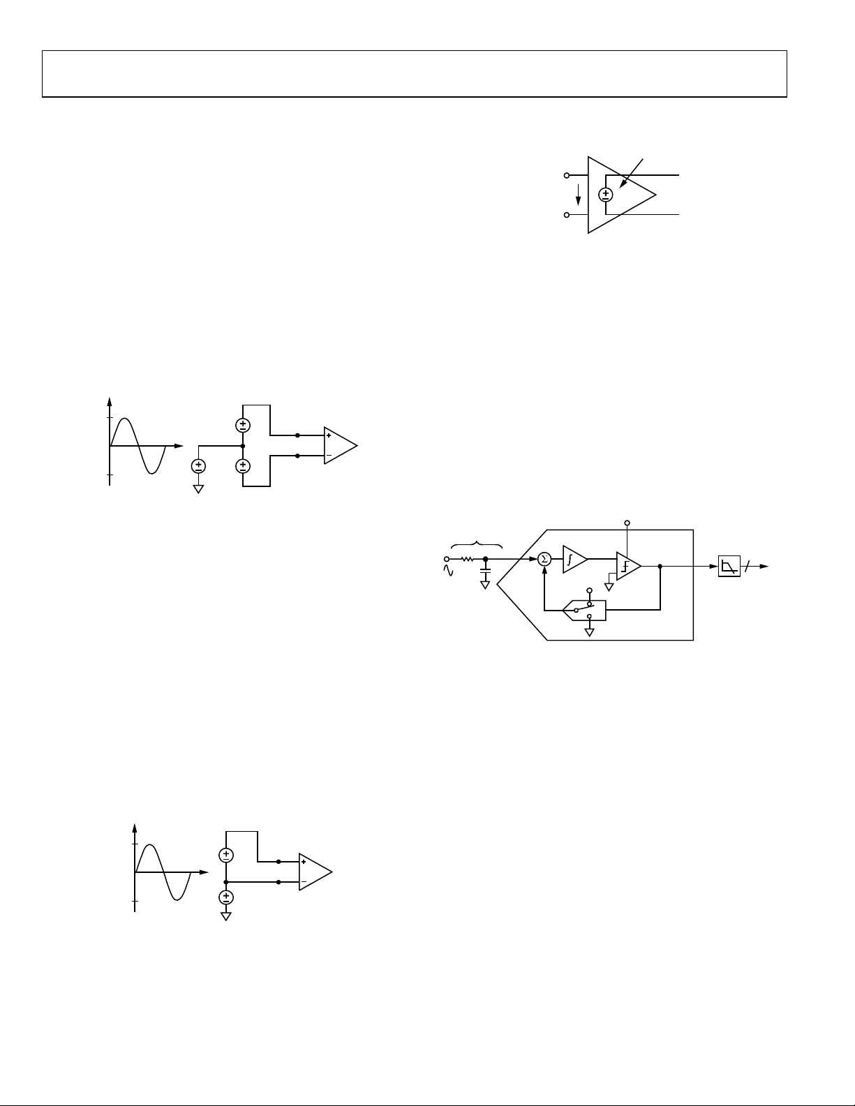
common-mode signal allowed on the inputs is ±25 mV. Figure 25
presents a schematic of the input for the current channels and
their relation to the maximum common-mode voltage.
DIFFERENTIAL INPUT
+ V2 = 500mV MAX PEAK
V
1
V1+ V
2
500m
V
CM
500m
Figure 25. Maximum Input Level, Current Channels, Gain = 1
All inputs have a programmable gain amplifier (PGA) with a
possible gain selection of 1, 2, 4, 8, or 16. The gain of IA, IB, and
IC inputs is set in Bits[2:0] (PGA1[2:0]) of the gain register. For
the ADE7868 and ADE7878 only, the gain of the IN input is set
in Bits[5:3] (PGA2[2:0]) of the gain register; thus, a different gain
from the IA, IB, or IC inputs is possible. See Table 44 for details
on the gain register.
The voltage channel has three single-ended voltage inputs: VAP,
VBP, and VCP. These single-ended voltage inputs have a maximum
input voltage of ±0.5 V with respect to VN. In addition, the maximum signal level on analog inputs for VxP and VN is ±0.5 V
with respect to AGND. The maximum common-mode signal
allowed on the inputs is ±25 mV. Figure 26 presents a schematic
of the voltage channels inputs and their relation to the maximum
common-mode voltage.
V
1
500m
V
CM
500m
Figure 26. Maximum Input Level, Voltage Channels, Gain = 1
All inputs have a programmable gain with a possible gain
selection of 1, 2, 4, 8, or 16. To set the gain, use Bits[8:6]
(PGA3[2:0]) in the gain register (see Table 44 ).
Figure 27 shows how the gain selection from the gain register
works in both current and voltage channels.
COMMON MODE
= ±25mV MAX
V
CM
V
1
V
DIFFERENTIAL INPUT
+ V2 = 500mV MAX PEAK
V
1
COMMON MODE
V
CM
= ±25mV MAX
CM
V
1
V
CM
V
2
VAP, VBP,
OR VCP
IAP, IBP,
ICP, OR INP
IAN, IBN,
ICN, OR INN
VN
08510-010
08510-012
Rev. E | Page 26 of 96
GAIN
SELECTION
IxP, VyP
V
IN
IxN, VN
NOTES
1. x = A, B, C, N
y = A, B, C.
K × V
IN
08510-011
Figure 27. PGA in Current and Voltage Channels
ANALOG-TO-DIGITAL CONVERSION
The ADE7868/ADE7878 have seven sigma-delta (Σ-) analogto-digital converters (ADCs), and the ADE7854/ADE7858 have
six Σ- ADCs. In PSM0 mode, all ADCs are active. In PSM1
mode, only the ADCs that measure the Phase A, Phase B, and
Phase C currents are active. The ADCs that measure the neutral
current and the A, B, and C phase voltages are turned off. In
PSM2 and PSM3 modes, the ADCs are powered down to
minimize power consumption.
For simplicity, the block diagram in Figure 28 shows a firstorder Σ- ADC. The converter is composed of the Σ- modulator
and the digital low-pass filter.
V
REF
CLKIN/16
+
–
.....10100101.....
1-BIT DAC
LATCHED
COMPARATOR
Σ
-∆ ADC
DIGITAL
LOW-PASS
FILTER
24
ANALOG
LOW-PASS FILTER
R
C
INTEGRATO R
+
–
Figure 28. First-Order
A Σ- modulator converts the input signal into a continuous
serial stream of 1s and 0s at a rate determined by the sampling
clock. In the ADE7854/ADE7858/ADE7868/ADE7878, the
sampling clock is equal to 1.024 MHz (CLKIN/16). The 1-bit
DAC in the feedback loop is driven by the serial data stream.
The DAC output is subtracted from the input signal. If the loop
gain is high enough, the average value of the DAC output (and,
therefore, the bit stream) can approach that of the input signal
level. For any given input value in a single sampling interval, the
data from the 1-bit ADC is virtually meaningless. Only when a
large number of samples are averaged is a meaningful result
obtained. This averaging is carried out in the second part of the
ADC, the digital low-pass filter. By averaging a large number of
bits from the modulator, the low-pass filter can produce 24-bit
data-words that are proportional to the input signal level.
The Σ- converter uses two techniques to achieve high resolution from what is essentially a 1-bit conversion technique. The
first is oversampling. Oversampling means that the signal is
sampled at a rate (frequency) that is many times higher than
the bandwidth of interest. For example, the sampling rate in
the ADE7854/ADE7858/ADE7868/ADE7878 is 1.024 MHz,
08510-013
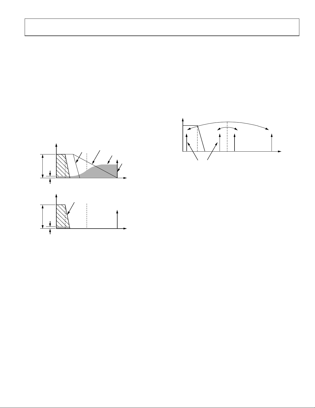
ADE7854/ADE7858/ADE7868/ADE7878
A
and the bandwidth of interest is 40 Hz to 2 kHz. Oversampling
has the effect of spreading the quantization noise (noise due to
sampling) over a wider bandwidth. With the noise spread more
thinly over a wider bandwidth, the quantization noise in the band
of interest is lowered, as shown in Figure 29. However, oversampling alone is not efficient enough to improve the signal-to-noise
ratio (SNR) in the band of interest. For example, an oversampling
factor of 4 is required just to increase the SNR by a mere 6 dB
(1 bit). To keep the oversampling ratio at a reasonable level, it is
possible to shape the quantization noise so that the majority of
the noise lies at the higher frequencies. In the Σ- modulator,
the noise is shaped by the integrator, which has a high-pass-type
response for the quantization noise. This is the second technique
used to achieve high resolution. The result is that most of the
noise is at the higher frequencies where it can be removed by
the digital low-pass filter. This noise shaping is shown in Figure 29.
ANTIALIAS FILTER
SIGNAL
NOISE
SIGNAL
NOISE
Figure 29. Noise Reduction Due to Oversampling and
DIGITAL FILTER
0 2 4 512
0 2 4 512
FREQUENCY (kHz)
HIGH RESOLUTION
OUTPUT FROM
DIGITAL LPF
FREQUENCY (kHz)
Noise Shaping in the Analog Modulator
(RC)
SHAPED NOISE
1024
1024
SAMPLING
FREQUENCY
08510-014
Antialiasing Filter
Figure 28 also shows an analog low-pass filter (RC) on the input
to the ADC. This filter is placed outside the ADE7854/ADE7858/
ADE7868/ADE7878, and its role is to prevent aliasing. Aliasing
is an artifact of all sampled systems as shown in Figure 30. Aliasing
means that frequency components in the input signal to the
ADC, which are higher than half the sampling rate of the ADC,
appear in the sampled signal at a frequency below half the
sampling rate. Frequency components above half the sampling
frequency (also known as the Nyquist frequency, that is, 512 kHz)
are imaged or folded back down below 512 kHz. This happens
with all ADCs regardless of the architecture. In the example shown,
only frequencies near the sampling frequency, that is, 1.024 MHz,
move into the band of interest for metering, that is, 40 Hz to
2 kHz. To attenuate the high frequency (near 1.024 MHz) noise
and prevent the distortion of the band of interest, a low-pass
filer (LPF) must be introduced. For conventional current
sensors, it is recommended to use one RC filter with a corner
frequency of 5 kHz for the attenuation to be sufficiently high at
the sampling frequency of 1.024 MHz. The 20 dB per decade
attenuation of this filter is usually sufficient to eliminate the
effects of aliasing for conventional current sensors. However, for a
di/dt sensor such as a Rogowski coil, the sensor has a 20 dB per
decade gain. This neutralizes the 20 dB per decade attenuation
produced by the LPF. Therefore, when using a di/dt sensor, take
care to offset the 20 dB per decade gain. One simple approach is
to cascade one additional RC filter, thereby producing a −40 dB
per decade attenuation.
LIASING E FFECTS
0 2 4 512
IMAGE
FREQUENCIES
FREQUENCY (kHz)
Figure 30. Aliasing Effects
SAMPLING
FREQUENCY
1024
08510-015
ADC Transfer Function
All ADCs in the ADE7854/ADE7858/ADE7868/ADE7878 are
designed to produce the same 24-bit signed output code for the
same input signal level. With a full-scale input signal of 0.5 V
and an internal reference of 1.2 V, the ADC output code is nominally 5,928,256 (0x5A7540). The code from the ADC can vary
between 0x800000 (−8,388,608) and 0x7FFFFF (+8,388,607);
this is equivalent to an input signal level of ±0.707 V. However,
for specified performance, do not exceed the nominal range of
±0.5 V; ADC performance is guaranteed only for input signals
lower than ±0.5 V.
CURRENT CHANNEL ADC
Figure 31 shows the ADC and signal processing path for
Input IA of the current channels (it is the same for IB and IC).
The ADC outputs are signed twos complement 24-bit datawords and are available at a rate of 8 kSPS (thousand samples
per second). With the specified full-scale analog input signal
of ±0.5 V, the ADC produces its maximum output code value.
Figure 31 shows a full-scale voltage signal applied to the differential inputs (IAP and IAN). The ADC output swings between
−5,928,256 (0xA58AC0) and +5,928,256 (0x5A7540). The
input, IN, corresponds to the neutral current of a 3-phase
system (available in the ADE7868 and ADE7878 only). If no
neutral line is present, connect this input to AGND. The
datapath of the neutral current is similar to the path of the
phase currents as shown in Figure 32.
Rev. E | Page 27 of 96
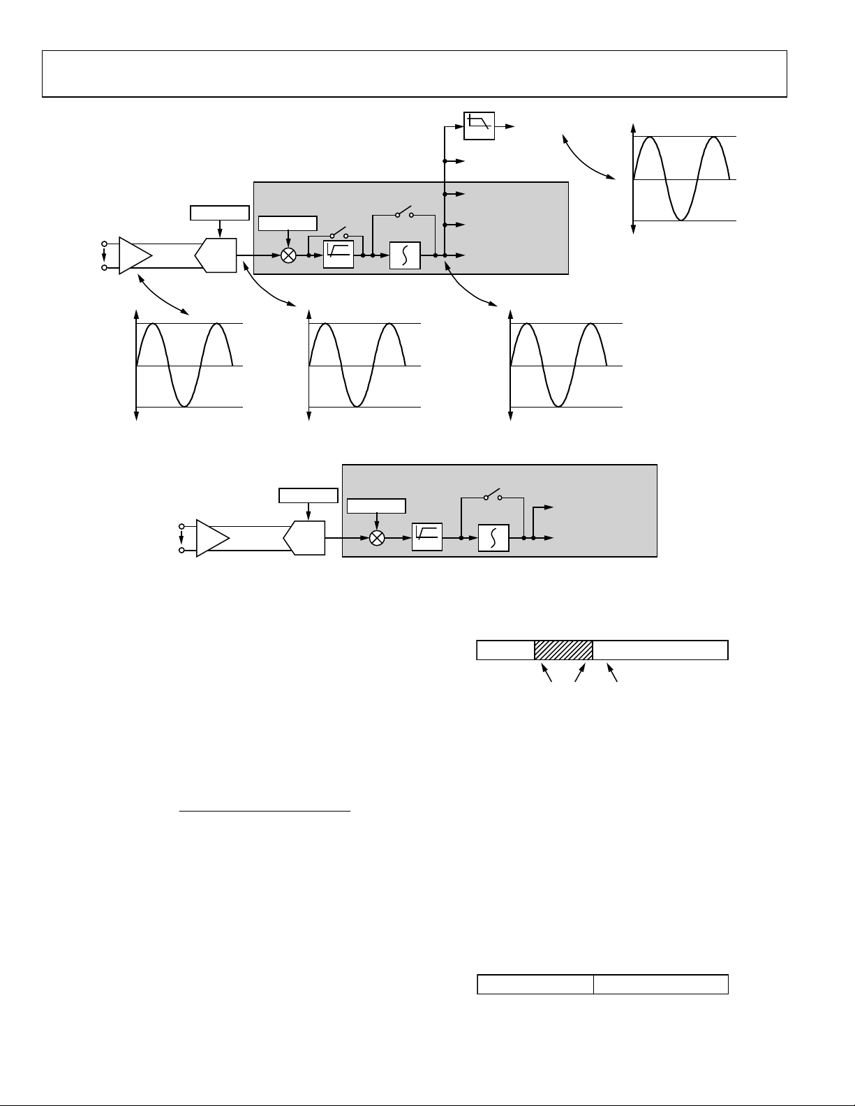
ADE7854/ADE7858/ADE7868/ADE7878
A
DSP
×1, ×2, ×4, ×8, ×16
IAP
V
IN
IAN
+0.5V/GAIN
–0.5V/GAIN
PGA1 BITS
GAIN[2:0]
PGA1
V
IN
0V
ANALOG INP UT RANGE ANALOG OUT PUT RANGE
REFERENCE
ADC
AIGAIN[23:0]
0x5A7540 =
+5,928,256
0xA58AC0 =
–5,928,256
HPFDIS
[23:0]
HPF
CURRENT CHANNE L
DATA RANGE
0V
INTEGRATOR
Figure 31. Current Channel Signal Path
DSP
PGA2 BITS
GAIN[5:3]
×1, ×2, ×4, ×8, ×16
INP
V
PGA2
IN
INN
REFERENCE
ADC
NIGAIN[23:0]
Figure 32. Neutral Current Signal Path (ADE7868, ADE7878 Only)
Current Waveform Gain Registers
There is a multiplier in the signal path of each phase and
neutral current. The current waveform can be changed by
±100% by writing a corresponding twos complement number
to the 24-bit signed current waveform gain registers (AIGAIN,
BIGAIN, CIGAIN, and NIGAIN). For example, if 0x400000 is
written to those registers, the ADC output is scaled up by 50%.
To scale the input by −50%, write 0xC00000 to the registers.
Equation 3 describes mathematically the function of the current
waveform gain registers.
Current Waveform =
⎛
OutputADC (3)
1
⎜
+×
⎜
⎝
23
2
RegisterGainCurrentofContent
⎞
⎟
⎟
⎠
Changing the content of the AIGAIN, BIGAIN, CIGAIN, or
INGAIN registers affects all calculations based on its current;
that is, it affects the corresponding phase active/reactive/
apparent energy and current rms calculation. In addition,
waveform samples scale accordingly.
Note that the serial ports of the ADE7854, ADE7858, ADE7868,
and/or ADE7878 work on 32-, 16-, or 8-bit words, and the DSP
works on 28 bits. The 24-bit AIGAIN, BIGAIN, CIGAIN, and
NIGAIN registers are accessed as 32-bit registers with the four
INTEN BIT
CONFIG[ 0]
DIGITAL
ZX SIGN
L
DATA RANG E
0V
08510-120
HPF
0V
DIGITAL
ZX DETECTION
CURRENT CHANNE L
DATA RANGE AFTER
LPF1
CURRENT PEAK,
OVERCURRENT
DETECT
CURRENT RMS (IRMS)
CALCULATION
IAWV WAVEFORM
SAMPLE REGISTER
TOTAL/FUNDAMENTAL
ACTIVE AND REACTIVE
POWER CALCULATION
0x5A7540 =
+5,928,256
0xA58AC0 =
–5,928,256
INTEN BIT
CONFIG[0]
INTEGRATOR
0x5A7540 =
+5,928,256
0xA58AC0 =
–5,928,256
INTEGRATION
CURRENT RMS (IRMS)
CALCULATION
INWV WAVEFORM
SAMPLE REGISTER
most significant bits (MSBs) padded with 0s and sign extended
to 28 bits. See Figure 33 for details.
31 28 27 24 23 0
24-BIT NUMBER0000
BITS[27:24] ARE
EQUAL TO BIT 23
BIT 23 IS A SIGN BI T
Figure 33. 24-Bit xIGAIN Transmitted as 32-Bit Words
Current Channel HPF
The ADC outputs can contain a dc offset. This offset can create
errors in power and rms calculations. High-pass filters (HPFs)
are placed in the signal path of the phase and neutral currents
and of the phase voltages. If enabled, the HPF eliminates any dc
offset on the current channel. All filters are implemented in the
DSP and, by default, they are all enabled: the 24-bit HPFDIS
register is cleared to 0x00000000. All filters are disabled by
setting HPFDIS to any nonzero value.
As stated in the Current Waveform Gain Registers section, the
serial ports of the ADE78xx work on 32-, 16-, or 8-bit words.
The HPFDIS register is accessed as a 32-bit register with eight
MSBs padded with 0s. See Figure 34 for details.
31 24 23 0
24-BIT NUMBER0000 0000
Figure 34. 24-Bit HPFDIS Register Transmitted as 32-Bit Word
08510-019
08510-016
08510-017
Rev. E | Page 28 of 96
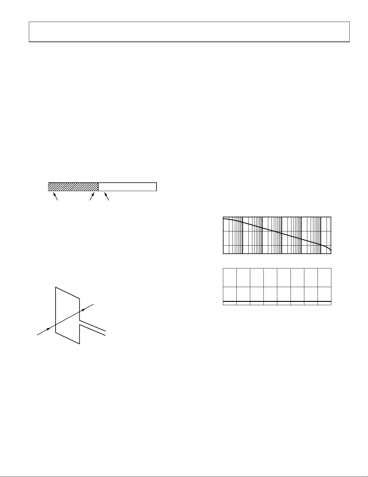
ADE7854/ADE7858/ADE7868/ADE7878
Current Channel Sampling
The waveform samples of the current channel are taken at the
output of HPF and stored in the 24-bit signed registers, IAWV,
IBWV, ICWV, and INWV (ADE7868 and ADE7878 only) at a
rate of 8 kSPS. All power and rms calculations remain uninterrupted during this process. Bit 17 (DREADY) in the STATUS0
register is set when the IAWV, IBWV, ICWV, and INWV registers
2
are available to be read using the I
C or SPI serial port. Setting
Bit 17 (DREADY) in the MASK0 register enables an interrupt
to be set when the DREADY flag is set. See the Digital Signal
Processor section for more details on Bit DREADY.
As stated in the Current Waveform Gain Registers section, the
serial ports of the ADE78xx work on 32-, 16-, or 8-bit words.
When the IAWV, IBWV, ICWV, and INWV 24-bit signed
registers are read from the ADE78xx (INWV is available on
ADE7868/ADE7878 only), they are transmitted sign extended
to 32 bits. See Figure 35 for details.
31 24 23 22 0
24-BIT SIG NED NUMBER
BITS[31:24] ARE
EQUAL TO BI T 23
Figure 35. 24-Bit IxWV Register Transmitted as 32-Bit Signed Word
BIT 23 IS A SIGN BI T
08510-018
The ADE7854/ADE7858/ADE7868/ADE7878 devices each
contain a high speed data capture (HSDC) port that is specially
designed to provide fast access to the waveform sample registers.
See the HSDC Interface section for more details.
di/dt CURRENT SENSOR AND DIGITAL INTEGRATOR
The di/dt sensor detects changes in the magnetic field caused by
the ac current. Figure 36 shows the principle of a di/dt current
sensor.
loop generate an electromotive force (EMF) between the two
ends of the loop. The EMF is a voltage signal that is proportional to the di/dt of the current. The voltage output from the
di/dt current sensor is determined by the mutual inductance
between the current carrying conductor and the di/dt sensor.
Due to the di/dt sensor, the current signal needs to be filtered
before it can be used for power measurement. On each phase and
neutral current datapath, there is a built-in digital integrator to
recover the current signal from the di/dt sensor. The digital integrator is disabled by default when the ADE78xx is powered up
and after a reset. Setting Bit 0 (INTEN) of the CONFIG register
turns on the integrator. Figure 37 and Figure 38 show the
magnitude and phase response of the digital integrator.
Note that the integrator has a −20 dB/dec attenuation and
approximately −90° phase shift. When combined with a di/dt
sensor, the resulting magnitude and phase response should be a
flat gain over the frequency band of interest. However, the di/dt
sensor has a 20 dB/dec gain associated with it and generates significant high frequency noise. An antialiasing filter of at least
the second order is needed to avoid noise aliasing back in the
band of interest when the ADC is sampling (see the Antialiasing
Filter section).
50
0
–50
MAGNITUDE (d B)PHASE (Degrees)
0.01 0.1 1 10 100 1000
0
–50
FREQUENCY (Hz)
MAGNETIC F IELD CREATED BY CURRENT
(DIRECTLY PROPORTIONAL TO CURRENT)
+ EMF (ELE CTROMOT IVE FORCE )
– INDUCED BY CHANGES IN
MAGNETIC FLUX DENSITY (di/dt)
Figure 36. Principle of a di/dt Current Sensor
The flux density of a magnetic field induced by a current is
directly proportional to the magnitude of the current. The
changes in the magnetic flux density passing through a conductor
Rev. E | Page 29 of 96
–100
0 500 1000 1500 2000 2500 3000 3 500 4000
Figure 37. Combined Gain and Phase Response of the
FREQUENCY (Hz)
Digital Integrator
08510-116
The DICOEFF 24-bit signed register is used in the digital
08510-020
integrator algorithm. At power-up or after a reset, its value is
0x000000. Before turning on the integrator, this register must be
initialized with 0xFFF8000. DICOEFF is not used when the
integrator is turned off and can remain at 0x000000 in that case.
 Loading...