Single-Phase Active and Apparent
FEATURES
High accuracy; supports IEC 61036/60687, IEC62053-21, and
IEC62053-22
On-chip digital integrator enables direct interface-to-current
sensors with di/dt output
A PGA in the current channel allows direct interface to
shunts and current transformers
Active and apparent energy, sampled waveform, and current
and voltage rms
Less than 0.1% error in active energy measurement over a
dynamic range of 1000 to 1 at 25°C
Positive-only energy accumulation mode available
On-chip user programmable threshold for line voltage surge
and SAG and PSU supervisory
Digital calibration for power, phase, and input offset
On-chip temperature sensor (±3°C typical)
SPI®-compatible serial interface
Pulse output with programmable frequency
Interrupt request pin (
Reference 2.4 V with external overdrive capability
Single 5 V supply, low power (25 mW typical)
GENERAL DESCRIPTION
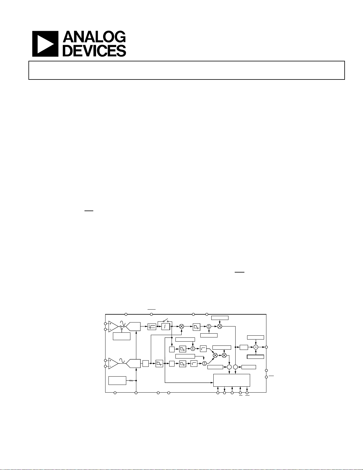
The ADE77631 features proprietary ADCs and fixed function
DSP for high accuracy over large variations in environmental
conditions and time. The ADE7763 incorporates two secondorder, 16-bit Σ-∆ ADCs, a digital integrator (on Ch1), reference
circuitry, a temperature sensor, and all the signal processing
) and status register
IRQ
PGA
V1P
V1N
V2P
V2N
TEMP
SENSOR
PGA
2.4V
REFERENCE
AVDD
FUNCTIONAL BLOCK DIAGRAM
RESET
INTEGRATOR
HPF1
LPF1
dt
2
x
2
x
ADC
Φ
ADC
PHCAL[5:0]
4k
Ω
MULTIPLIER
IRMSOS[11:0]
VRMSOS[11:0]
Energy Metering IC
ADE7763
required to perform active and apparent energy measurements,
line-voltage period measurements, and rms calculation on the
voltage and current channels. The selectable on-chip digital
integrator provides direct interface to di/dt current sensors such
as Rogowski coils, eliminating the need for an external analog
integrator and resulting in excellent long-term stability and
precise phase matching between the current and the voltage
channels.
The ADE7763 provides a serial interface to read data and a
pulse output frequency (CF) that is proportional to the active
power. Various system calibration features such as channel
offset correction, phase calibration, and power calibration
ensure high accuracy. The part also detects short duration, low
or high voltage variations.
The positive-only accumulation mode gives the option to
accumulate energy only when positive power is detected. An
internal no-load threshold ensures that the part does not exhibit
any creep when there is no load. The zero-crossing output (ZX)
produces a pulse that is synchronized to the zero-crossing point
of the line voltage. This signal is used internally in the line cycle
active and apparent energy accumulation modes, which enables
faster calibration.
The interrupt status register indicates the nature of the interrupt,
and the interrupt enable register controls which event produces
an output on the
The ADE7763 is available in a 20-lead SSOP package.
DVDD DGND
APOS[15:0]
VADIV[7:0]
WGAIN[11:0]
VAGAIN[11:0]
REGISTERS AND
SERIAL INTERFACE
LPF2
pin, an open-drain, active low logic output.
IRQ
ADE7763
CFNUM[11:0]
% %
DFC
CFDEN[11:0]
WDIV[7:0]
CF
ZX
SAG
CLKOUT
AGND
1
U.S. Patents 5,745,323; 5,760,617; 5,862,069; 5,872,469; others pending.
Rev. A
Information furnished by Analog Devices is believed to be accurate and reliable.
However, no responsibility is assumed by Analog Devices for its use, nor for any
infringements of patents or other rights of third parties that may result from its use.
Specifications subject to change without notice. No license is granted by implication
or otherwise under any patent or patent rights of Analog Devices. Trademarks and
registered trademarks are the property of their respective owners.
IN/OUT
CLKIN
Figure 1.
DIN DOUT SCLKREF
CS IRQ
04481-A-001
One Technology Way, P.O. Box 9106, Norwood, MA 02062-9106, U.S.A.
Tel: 781.329.4700
www.analog.com
Fax: 781.326.8703 © 2004 Analog Devices, Inc. All rights reserved.

ADE7763
TABLE OF CONTENTS
Specifications..................................................................................... 3
Energy-to-Frequency Conversion............................................ 28
Timing Characteristics..................................................................... 5
Absolute Maximum Ratings............................................................ 6
ESD Caution.................................................................................. 6
Te r mi n ol o g y ...................................................................................... 7
Pin Configuration and Function Descriptions............................. 8
Typical Performance Characteristics........................................... 10
Theory of Operation ...................................................................... 13
Analog Inputs.............................................................................. 13
di/dt Current Sensor and Digital Integrator........................... 14
Zero-Crossing Detection........................................................... 15
Period Measurement.................................................................. 16
Power Supply Monitor ...............................................................16
Line Voltage Sag Detection....................................................... 17
Peak Detection ............................................................................17
Interrupts..................................................................................... 18
Line Cycle Energy Accumulation Mode ................................. 30
Positive-Only Accumulation Mode......................................... 30
No-Load Threshold.................................................................... 30
Apparent Power Calculation ..................................................... 31
Apparent Energy Calculation ................................................... 32
Line Apparent Energy Accumulation...................................... 33
Energies Scaling.......................................................................... 34
Calibrating an Energy Meter .................................................... 34
CLKIN Frequency...................................................................... 43
Suspending Functionality.......................................................... 44
Checksum Register..................................................................... 44
Serial Interface............................................................................ 44
Registers........................................................................................... 47
Register Descriptions..................................................................... 50
Communication Register.......................................................... 50
Temperature Measurement ....................................................... 19
Analog-to-Digital Conversion.................................................. 19
Channel 1 ADC .......................................................................... 20
Channel 2 ADC .......................................................................... 22
Phase Compensation.................................................................. 24
Active Power Calculation .......................................................... 25
Energy Calculation..................................................................... 26
Power Offset Calibration ...........................................................28
REVISION HISTORY
10/04—Data Sheet Changed from Rev. 0 to Rev. A
Changes to Period Measurement Section ..................................16
Changes to Temperature Measurement Section........................19
Change to Energy-to-Frequency Conversion Section..............28
Update to Figure 61 .......................................................................29
Mode Register (0x09)................................................................. 50
Interrupt Status Register (0x0B), Reset Interrupt Status
Register (0x0C), Interrupt Enable Register (0x0A)
CH1OS Register (0x0D)............................................................ 53
Outline Dimensions ....................................................................... 54
Ordering Guide .......................................................................... 54
Change to Apparent Energy Calculation Section .....................32
Change to Description of AEHF and VAEHF Bits ................... 52
4/04—Revision 0: Initial Version
............... 52
Rev. A | Page 2 of 56

ADE7763
SPECIFICATIONS
AVDD = DVDD = 5 V ± 5%, AGND = DGND = 0 V, on-chip reference, CLKIN = 3.579545 MHz XTAL, T
Table 1. Specifications
1, 2
Parameter Spec Unit Test Conditions/Comments
ENERGY MEASUREMENT ACCURACY
Active Power Measurement Error CLKIN = 3.579545 MHz
Channel 1 Range = 0.5 V Full Scale Channel 2 = 300 mV rms/60 Hz, gain = 2
Gain = 1 0.1 % typ Over a dynamic range 1000 to 1
Gain = 2 0.1 % typ Over a dynamic range 1000 to 1
Gain = 4 0.1 % typ Over a dynamic range 1000 to 1
Gain = 8 0.1 % typ Over a dynamic range 1000 to 1
Channel 1 Range = 0.25 V Full Scale
Gain = 1 0.1 % typ Over a dynamic range 1000 to 1
Gain = 2 0.1 % typ Over a dynamic range 1000 to 1
Gain = 4 0.1 % typ Over a dynamic range 1000 to 1
Gain = 8 0.2 % typ Over a dynamic range 1000 to 1
Channel 1 Range = 0.125 V Full Scale
Gain = 1 0.1 % typ Over a dynamic range 1000 to 1
Gain = 2 0.1 % typ Over a dynamic range 1000 to 1
Gain = 4 0.2 % typ Over a dynamic range 1000 to 1
Gain = 8 0.2 % typ Over a dynamic range 1000 to 1
Active Power Measurement Bandwidth 14 kHz
Phase Error 1 between Channels ±0.05 max Line frequency = 45 Hz to 65 Hz, HPF on
AC Power Supply Rejection
1
AVDD = DVDD = 5 V + 175 mV rms/120 Hz
Output Frequency Variation (CF) 0.2 % typ Channel 1 = 20 mV rms, gain = 16, range = 0.5 V
Channel 2 = 300 mV rms/60 Hz, gain = 1
DC Power Supply Rejection
1
AVDD = DVDD = 5 V ± 250 mV dc
Output Frequency Variation (CF) ±0.3 % typ Channel 1 = 20 mV rms/60 Hz, gain = 16, range = 0.5 V
Channel 2 = 300 mV rms/60 Hz, gain = 1
IRMS Measurement Error 0.5 % typ Over a dynamic range 100 to 1
IRMS Measurement Bandwidth 14 kHz
VRMS Measurement Error 0.5 % typ Over a dynamic range 20 to 1
VRMS Measurement Bandwidth 140 Hz
ANALOG INPUTS
3
See the Analog Inputs section
Maximum Signal Levels ±0.5 V max V1P, V1N, V2N, and V2P to AGND
Input Impedance (dc) 390 k min
Bandwidth 14 kHz CLKIN/256, CLKIN = 3.579545 MHz
Gain Error
1, 3
External 2.5 V reference, gain = 1 on Channels 1 and 2
Channel 1
Range = 0.5 V Full Scale ±4 % typ V1 = 0.5 V dc
Range = 0.25 V Full Scale ±4 % typ V1 = 0.25 V dc
Range = 0.125 V Full Scale ±4 % typ V1 = 0.125 V dc
Channel 2 ±4 % typ V2 = 0.5 V dc
Offset Error 1 ±32 mV max Gain 1
Channel 1 ±13 mV max Gain 16
±32 mV max Gain 1
Channel 2 ±13 mV max Gain 16
MIN
to T
= –40°C to +85°C.
MAX
Rev. A | Page 3 of 56

ADE7763
T
Parameter Spec Unit Test Conditions/Comments
WAVEFORM SAMPLING Sampling CLKIN/128, 3.579545 MHz/128 = 27.9 kSPS
Channel 1 See the Channel 1 Sampling section
Signal-to-Noise Plus Distortion 62 dB typ 150 mV rms/60 Hz, range = 0.5 V, gain = 2
Bandwidth (–3 dB) 14 kHz CLKIN = 3.579545 MHz
Channel 2 See the Channel 2 Sampling section
Signal-to-Noise Plus Distortion 60 dB typ 150 mV rms/60 Hz, gain = 2
Bandwidth (–3 dB) 140 Hz CLKIN = 3.579545 MHz
REFERENCE INPUT
REF
2.2 V min 2.4 V – 8%
Input Capacitance 10 pF max
ON-CHIP REFERENCE Nominal 2.4 V at REF
Reference Error ±200 mV max
Current Source 10 µA max
Output Impedance 3.4 kΩ min
Temperature Coefficient 30 ppm/°C typ
CLKIN All specifications CLKIN of 3.579545 MHz
Input Clock Frequency 4 MHz max
1 MHz min
LOGIC INPUTS
RESET, DIN, SCLK, CLKIN, and CS
Input High Voltage, V
Input Low Voltage, V
Input Current, I
Input Capacitance, C
LOGIC OUTPUTS
SAG and IRQ
Output High Voltage, V
Output Low Voltage, V
ZX and DOUT
Output High Voltage, V
Output Low Voltage, V
CF
Output High Voltage, V
Output Low Voltage, V
POWER SUPPLY For specified performance
AVDD 4.75 V min 5 V – 5%
5.25 V max 5 V + 5%
DVDD 4.75 V min 5 V – 5%
5.25 V max 5 V + 5%
AIDD 3 mA max Typically 2.0 mA
DIDD 4 mA max Typically 3.0 mA
_______________________ ________________________________ ___
1
See the Terminology section for explanation of specifications.
2
See the plots in the Typical Performance Characteristics section.
3
See the Analog Inputs section.
Input Voltage Range 2.6 V max 2.4 V + 8%
IN/OUT
INH
INL
IN
IN
2.4 V min DVDD = 5 V ± 10%
0.8 V max DVDD = 5 V ± 10%
±3 µA max Typically 10 nA, VIN = 0 V to DVDD
10 pF max
Open-drain outputs, 10 kΩ pull-up resistor
OH
OL
OH
OL
OH
OL
4 V min I
0.4 V max I
4 V min I
0.4 V max I
4 V min I
1 V max I
200 µA
SOURCE
= 0.8 mA
SINK
SOURCE
= 0.8 mA
SINK
SOURCE
= 7 mA
SINK
I
Ol
= 5 mA
= 5 mA
= 5 mA
IN/OUT
pin
OUTPU
TO
PIN
50pF
C
L
1.6mA
I
OH
+2.1V
04481-A-002
Figure 2. Load Circuit for Timing Specifications
Rev. A | Page 4 of 56
ADE7763
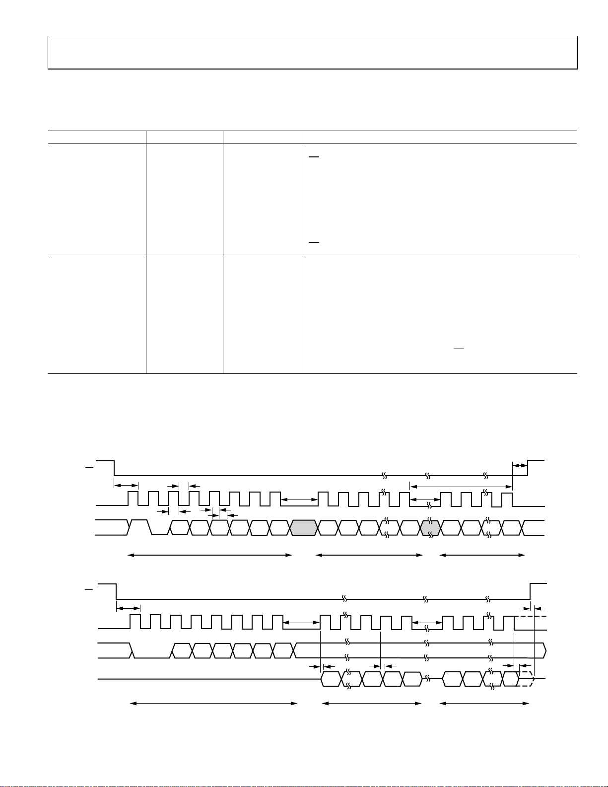
TIMING CHARACTERISTICS
AVDD = DVDD = 5 V ± 5%, AGND = DGND = 0 V, on-chip reference, CLKIN = 3.579545 MHz XTAL, T
Table 2. Timing Characteristics
1, 2
Parameter Spec Unit Test Conditions/Comments
Write Timing
t
1
t
2
t
3
t
4
t
5
t
6
t
7
t
8
50 ns min
CS falling edge to first SCLK falling edge.
50 ns min SCLK logic high pulse width.
50 ns min SCLK logic low pulse width.
10 ns min Valid data setup time before falling edge of SCLK.
5 ns min Data hold time after SCLK falling edge.
400 ns min Minimum time between the end of data byte transfers.
50 ns min Minimum time between byte transfers during a serial write.
100 ns min)
CS hold time after SCLK falling edge.
Read Timing
3
t
9
4 µs min
Minimum time between read command (i.e., a write to
communication register) and data read.
t
10
t
11
50 ns min Minimum time between data byte transfers during a multibyte read.
30 ns min
Data access time after SCLK rising edge following a write to the
communication register.
4
t
12
100 ns max Bus relinquish time after falling edge of SCLK.
10 ns min
5
t
13
10 ns min
________________________________________________
1
Sample tested during initial release and after any redesign or process change that could affect this parameter. All input signals are specified with tr = tf = 5 ns (10% to
90%) and timed from a voltage level of 1.6 V.
2
See Figure 3, Figure 4, and the Serial Interface section.
3
Minimum time between read command and data read for all registers except waveform register, which is t9 = 500 ns min.
4
Measured with the load circuit in Figure 2 and defined as the time required for the output to cross 0.8 V or 2.4 V.
5
Derived from the measured time taken by the data outputs to change 0.5 V when loaded with the circuit in Figure 2. The measured number is then extrapolated back
to remove the effects of charging or discharging the 50 pF capacitor. This means that the time quoted in the timing characteristics is the true bus relinquish time of
the part and is independent of the bus loading.
CS
SCLK
DIN
100 ns max
t
1
1
t
3
t
t
2
0
4
A4A5 A3
t
5
A2
Bus relinquish time after rising edge of
t
7
A0
A1
DB7
t
DB0
MIN
to T
= −40°C to +85°C.
MAX
CS.
t
8
t
6
7
DB7
DB0
SCLK
DIN
DOUT
CS
COMMAND BYTE
MOST SIGNIFICANT BYTE
LEAST SIGNIFICANT BYTE
04481-A-003
Figure 3. Serial Write Timing
t
1
t
9
0
0
A4A5 A3
COMMAND BYTE
A2
A0
A1
t
11
DB7
MOST SIGNIFICANT BYTE
t
10
t
11
DB0
LEAST SIGNIFICANT BYTE
t
13
t
12
DB0DB7
04481-A-004
Figure 4. Serial Read Timing
Rev. A | Page 5 of 56

ADE7763
ABSOLUTE MAXIMUM RATINGS
TA = 25°C, unless otherwise noted.
Table 3.
Parameter Rating
AVDD to AGND –0.3 V to +7 V
DVDD to DGND –0.3 V to +7 V
DVDD to AVDD –0.3 V to +0.3 V
Analog Input Voltage to AGND
V1P, V1N, V2P, and V2N
Reference Input Voltage to AGND –0.3 V to AVDD + 0.3 V
Digital Input Voltage to DGND –0.3 V to DVDD + 0.3 V
Digital Output Voltage to DGND –0.3 V to DVDD + 0.3 V
Operating Temperature Range
Industrial –40°C to +85°C
Storage Temperature Range –65°C to +150°C
Junction Temperature 150°C
20-Lead SSOP, Power Dissipation 450 mW
θJA Thermal Impedance 112°C/W
Lead Temperature, Soldering
Vapor Phase (60 s) 215°C
Infrared (15 s) 220°C
–6 V to +6 V
Stresses above those listed under Absolute Maximum Ratings
may cause permanent damage to the device. This is a stress
rating only, and functional operation of the device at these or
any other conditions above those indicated in the operational
section of this specification is not implied. Exposure to absolute
maximum rating conditions for extended periods may affect
device reliability.
ESD CAUTION
ESD (electrostatic discharge) sensitive device. Electrostatic charges as high as 4000 V readily accumulate on
the human body and test equipment and can discharge without detection. Although this product features
proprietary ESD protection circuitry, permanent damage may occur on devices subjected to high energy
electrostatic discharges. Therefore, proper ESD precautions are recommended to avoid performance
degradation or loss of functionality.
Rev. A | Page 6 of 56

ADE7763
TERMINOLOGY
Measurement Error
The error associated with the energy measurement made by the
ADE7763 is defined by the following formula:
Percent Error =
⎛
⎜
⎜
⎝
Phase Error between Channels
The digital integrator and the high-pass filter (HPF) in Channel 1
have a nonideal phase response. To offset this phase response
and equalize the phase response between channels, two phasecorrection networks are placed in Channel 1: one for the digital
integrator and the other for the HPF. The phase correction
networks correct the phase response of the corresponding
component and ensure a phase match between Channel 1
(current) and Channel 2 (voltage) to within ±0.1° over a range
of 45 Hz to 65 Hz with the digital integrator off. With the digital
integrator on, the phase is corrected to within ±0.4° over a
range of 45 Hz to 65 Hz.
Power Supply Rejection
This quantifies the ADE7763 measurement error as a percentage
of the reading when the power supplies are varied. For the ac
PSR measurement, a reading at nominal supplies (5 V) is taken.
A second reading is obtained with the same input signal levels
−
EnergyTrue
⎞
EnergyTrueADE7763RegisterEnergy
⎟
× 100%
⎟
⎠
when an ac (175 mV rms/120 Hz) signal is introduced to the
supplies. Any error introduced by this ac signal is expressed
as a percentage of the reading—see the Measurement
Error definition.
For the dc PSR measurement, a reading at nominal supplies
(5 V) is taken. A second reading is obtained with the same input
signal levels when the supplies are varied ±5%. Any error
introduced is again expressed as a percentage of the reading.
ADC Offset Error
The dc offset associated with the analog inputs to the ADCs. It
means that with the analog inputs connected to AGND, the
ADCs still see a dc analog input signal. The magnitude of the
offset depends on the gain and input range selection—see the
Typical Performance Characteristics section. However, when
HPF1 is switched on, the offset is removed from Channel 1
(current) and the power calculation is not affected by this offset.
The offsets can be removed by performing an offset calibration—
see the Analog Inputs section.
Gain Error
The difference between the measured ADC output code (minus
the offset) and the ideal output code—see the Channel 1 ADC
and Channel 2 ADC sections. It is measured for each of the
input ranges on Channel 1 (0.5 V, 0.25 V, and 0.125 V). The
difference is expressed as a percentage of the ideal code.
Rev. A | Page 7 of 56
ADE7763
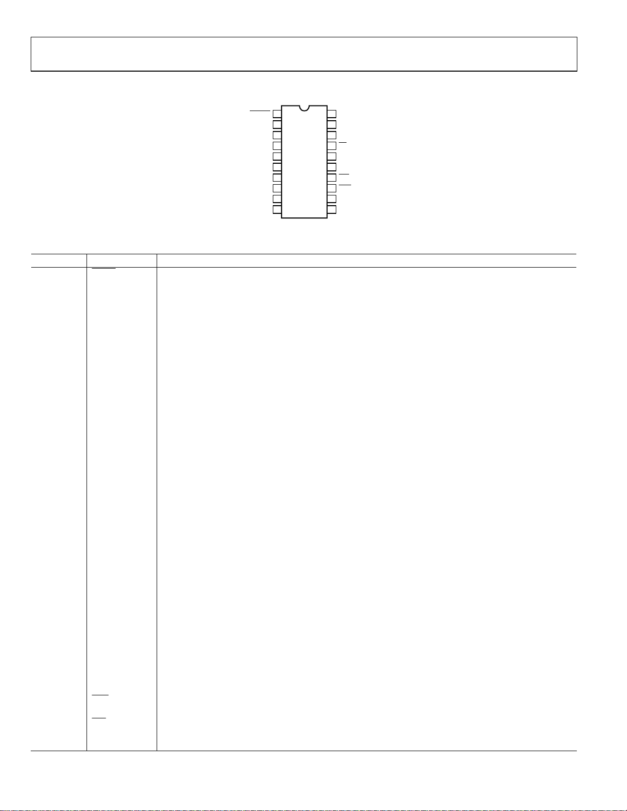
PIN CONFIGURATION AND FUNCTION DESCRIPTIONS
Table 4. Pin Function Descriptions
Pin No. Mnemonic Description
1
RESET Reset Pin for the ADE7763. A logic low on this pin holds the ADCs and digital circuitry (including the serial
interface) in a reset condition.
2 DVDD
Digital Power Supply. This pin provides the supply voltage for the digital circuitry. The supply voltage
should be maintained at 5 V ± 5% for specified operation. This pin should be decoupled to DGND with a
10 µF capacitor in parallel with a ceramic 100 nF capacitor.
3 AVDD
Analog Power Supply. This pin provides the supply voltage for the analog circuitry. The supply should be
maintained at 5 V ± 5% for specified operation. Minimize power supply ripple and noise at this pin by using
proper decoupling. The typical performance graphs show the power supply rejection performance. This
pin should be decoupled to AGND with a 10 µF capacitor in parallel with a ceramic 100 nF capacitor.
4, 5 V1P, V1N
Analog Inputs for Channel 1. This channel is intended for use with a di/dt current transducer, i.e., a
Rogowski coil or another current sensor such as a shunt or current transformer (CT). These inputs are fully
differential voltage inputs with maximum differential input signal levels of ±0.5 V, ±0.25 V, and ±0.125 V,
depending on the full-scale selection—see the Analog Inputs section. Channel 1 also has a PGA with gain
selections of 1, 2, 4, 8, or 16. The maximum signal level at these pins with respect to AGND is ±0.5 V. Both
inputs have internal ESD protection circuitry and can sustain an overvoltage of ±6 V without risk of
permanent damage.
6, 7 V2N, V2P
Analog Inputs for Channel 2. This channel is intended for use with the voltage transducer. These inputs are
fully differential voltage inputs with a maximum differential signal level of ±0.5 V. Channel 2 also has a PGA
with gain selections of 1, 2, 4, 8, or 16. The maximum signal level at these pins with respect to AGND is
±0.5 V. Both inputs have internal ESD protection circuitry and can sustain an overvoltage of ±6 V without
risk of permanent damage.
8 AGND
Analog Ground Reference. This pin provides the ground reference for the analog circuitry, i.e., ADCs and
reference. This pin should be tied to the analog ground plane or to the quietest ground reference in the
system. Use this quiet ground reference for all analog circuitry, such as antialiasing filters and current and
voltage transducers. To minimize ground noise around the ADE7763, connect the quiet ground plane
to the digital ground plane at only one point. It is acceptable to place the entire device on the analog
ground plane.
9 REF
IN/OUT
Access to the On-Chip Voltage Reference. The on-chip reference has a nominal value of 2.4 V ± 8% and a
typical temperature coefficient of 30 ppm/°C. An external reference source can also be connected at this
pin. In either case, this pin should be decoupled to AGND with a 1 µF ceramic capacitor.
10 DGND
Digital Ground Reference. This pin provides the ground reference for the digital circuitry, i.e., multiplier,
filters, and digital-to-frequency converter. Because the digital return currents in the ADE7763 are small, it is
acceptable to connect this pin to the analog ground plane of the system. However, high bus capacitance
on the DOUT pin could result in noisy digital current, which could affect performance.
11 CF
Calibration Frequency Logic Output. The CF logic output gives active power information. This output is
intended to be used for operational and calibration purposes. The full-scale output frequency can be
adjusted by writing to the CFDEN and CFNUM registers—see the Energy-to-Frequency Conversion section.
12 ZX
Voltage Waveform (Channel 2) Zero-Crossing Output. This output toggles logic high and logic low at the
zero crossing of the differential signal on Channel 2—see the Zero-Crossing Detection section.
13
SAG This open-drain logic output goes active low when either no zero crossings are detected or a low voltage
threshold (Channel 2) is crossed for a specified duration—see the Line Voltage Sag Detection section.
14
IRQ Interrupt Request Output. This is an active low, open-drain logic output. Maskable interrupts include active
energy register rollover, active energy register at half level, and arrivals of new waveform samples—see the
Interrupts section.
REF
RESET
DVDD
AVDD
V1P
V1N
V2N
V2P
AGND
IN/OUT
DGND
1
2
3
4
ADE7763
5
TOP VIEW
6
(Not to Scale)
7
8
9
10
20
19
18
17
16
15
14
13
12
11
DIN
DOUT
SCLK
CS
CLKOUT
CLKIN
IRQ
SAG
ZX
CF
04481-A-005
Figure 5. Pin Configuration (SSOP Package)
Rev. A | Page 8 of 56

ADE7763
Pin No. Mnemonic Description
15 CLKIN
16 CLKOUT
17
18 SCLK
19 DOUT
20 DIN
CS Chip Select. Part of the 4-wire SPI serial interface. This active low logic input allows the ADE7763 to share
Master Clock for ADCs and Digital Signal Processing. An external clock can be provided at this logic input.
Alternatively, a parallel resonant AT crystal can be connected across CLKIN and CLKOUT to provide a clock
source for the ADE7763. The clock frequency for specified operation is 3.579545 MHz. Ceramic load
capacitors between 22 pF and 33 pF should be used with the gate oscillator circuit. Refer to the crystal
manufacturer’s data sheet for load capacitance requirements.
A crystal can be connected across this pin and CLKIN, as described for Pin 15, to provide a clock source for
the ADE7763. The CLKOUT pin can drive one CMOS load when either an external clock is supplied at CLKIN
or a crystal is being used.
the serial bus with several other devices—see the Serial Interface section.
Serial Clock Input for the Synchronous Serial Interface. All serial data transfers are synchronized to this
clock—see the Serial Interface section. The SCLK has a Schmitt-trigger input for use with a clock source
that has a slow edge transition time, such as an opto-isolator output.
Data Output for the Serial Interface. Data is shifted out at this pin upon the rising edge of SCLK. This logic
output is normally in a high impedance state, unless it is driving data onto the serial data bus—see the
Serial Interface section.
Data Input for the Serial Interface. Data is shifted in at this pin upon the falling edge of SCLK—see the
Serial Interface section.
Rev. A | Page 9 of 56
ADE7763
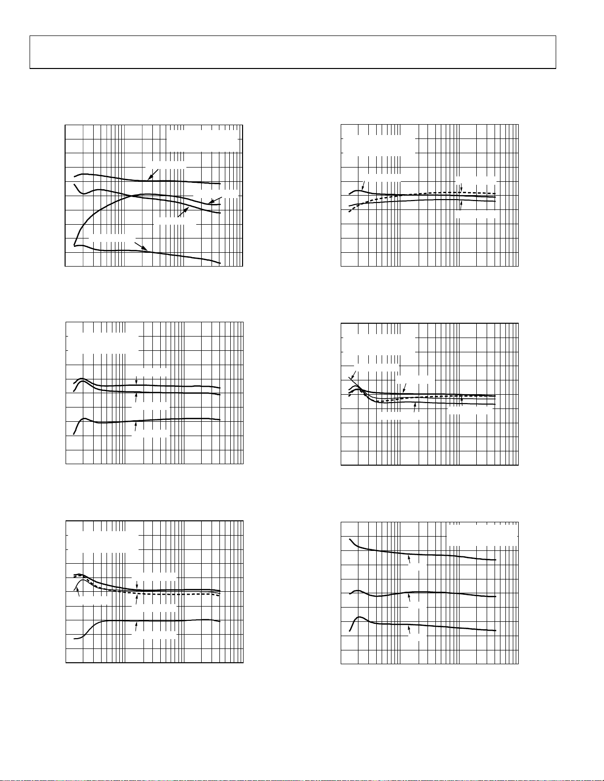
TYPICAL PERFORMANCE CHARACTERISTICS
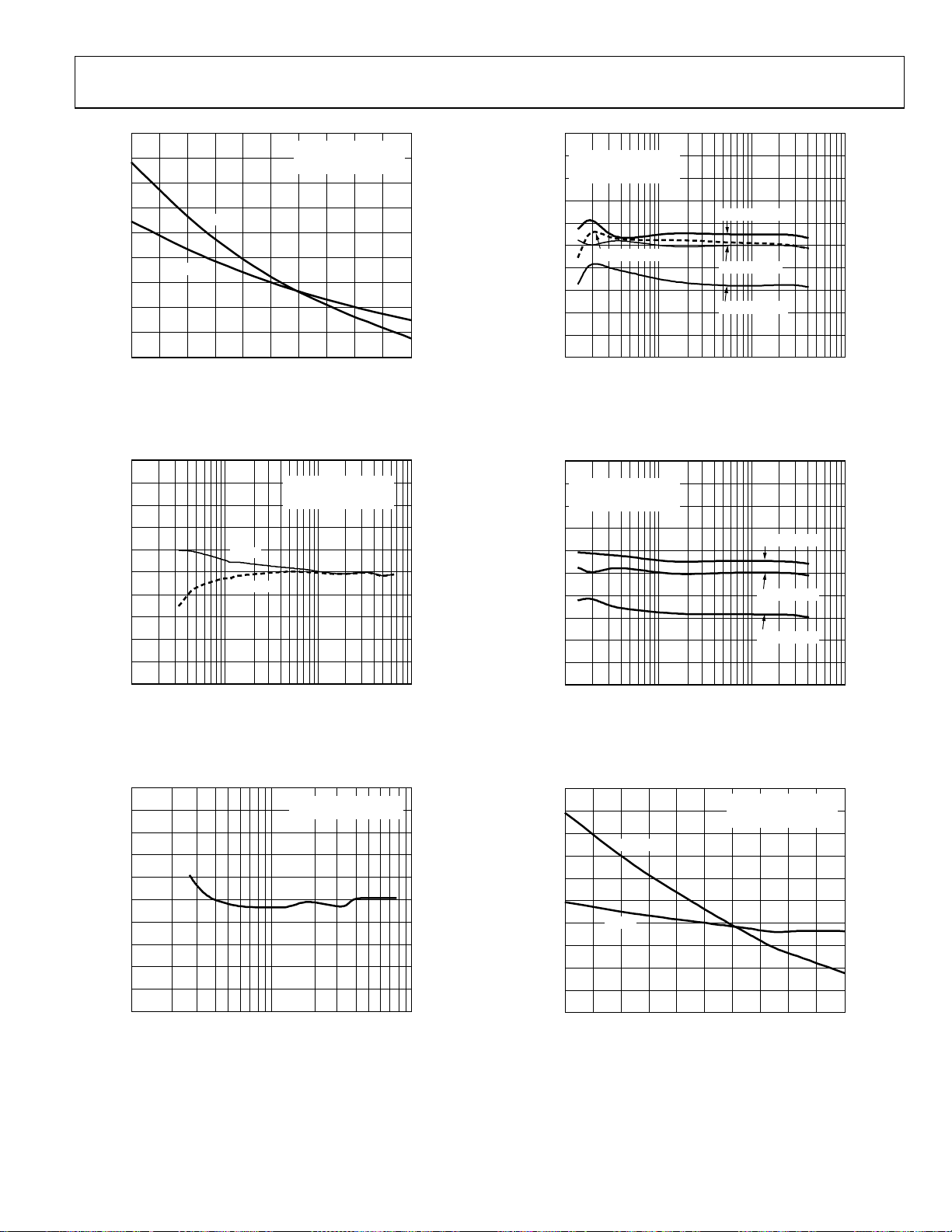
0.4
0.3
0.2
0.1
0
–0.1
–0.2
ERROR (%)
–0.3
–0.4
–0.5
–0.6
0.1
+85°C, PF = 0.5
1 10 100
FULL-SCALE CURRENT (%)
Figure 6. Active Energy Error as a Percentage of Reading (Gain = 1)
over Power Factor with Internal Reference and Integrator Off
1.0
0.8
GAIN = 8
INTEGRATOR OFF
INTERNAL REFERENCE
0.6
0.4
0.2
0
–0.2
ERROR (%)
–0.4
–0.6
–0.8
–1.0
0.1 101 100
+85°C, PF = 1
+25°C, PF = 1
–40°C, PF = 1
FULL-SCALE CURRENT (%)
Figure 7. Active Energy as a Percentage of Reading (Gain = 8)
over Temperature with Internal Reference and Integrator Off
1.0
0.8
GAIN = 8
INTEGRATOR OFF
INTERNAL REFERENCE
0.6
0.4
0.2
0
+25°C, PF = 1
–0.2
ERROR (%)
–0.4
–0.6
–0.8
–1.0
0.1 101 100
+85°C, PF = 0.5
+25°C, PF = 0.5
–40°C, PF = 0.5
FULL-SCALE CURRENT (%)
Figure 8. Active Energy Error as a Percentage of Reading (Gain = 8)
over Power Factor with Internal Reference and Integrator Off
GAIN = 1
INTEGRATOR OFF
INTERNAL REFERENCE
+25°C, PF = 1
+25°C, PF = 0.5
–40°C, PF = 0.5
04481-A-006
04481-A-007
04481-A-008
1.0
0.8
GAIN = 8
INTEGRATOR OFF
EXTERNAL REFERENCE
0.6
0.4
0.2
0
–0.2
ERROR (%)
–0.4
–0.6
–0.8
–1.0
+25°C, PF = 1
0.1 101 100
FULL-SCALE CURRENT (%)
–40°C, PF = 1
+85°C, PF = 1
Figure 9. Active Energy Error as a Percentage of Reading (Gain = 8)
over Temperature with External Reference and Integrator Off
1.0
0.8
GAIN = 8
INTEGRATOR OFF
EXTERNAL REFERENCE
0.6
0.4
+25°C, PF = 0.5
0.2
0
–0.2
ERROR (%)
–0.4
–0.6
–0.8
–1.0
0.1 101 100
+25°C, PF = 1
+85°C, PF = 0.5
FULL-SCALE CURRENT (%)
–40°C, PF = 0.5
Figure 10. Active Energy Error as a Percentage of Reading (Gain = 8)
over Power Factor with External Reference and Integrator Off
0.5
0.4
0.3
0.2
0.1
0
–0.1
ERROR (%)
–0.2
–0.3
–0.4
–0.5
0.1 101 100
5.25V
5.00V
4.75V
FULL-SCALE CURRENT (%)
GAIN = 8
INTEGRATOR OFF
INTERNAL REFERENCE
Figure 11. Active Energy Error as a Percentage of Reading (Gain = 8)
over Power Supply with Internal Reference and Integrator Off
04481-A-009
04481-A-010
04481-A-080
Rev. A | Page 10 of 56
ADE7763
1.2
1.0
0.8
0.6
0.4
0.2
ERROR (%)
0
–0.2
–0.4
–0.6
45 47 49 51 53 55 57 59 61 63 65
PF = 0.5
PF = 1
FREQUENCY (Hz)
GAIN = 8
INTEGRATOR OFF
INTERNAL REFERENCE
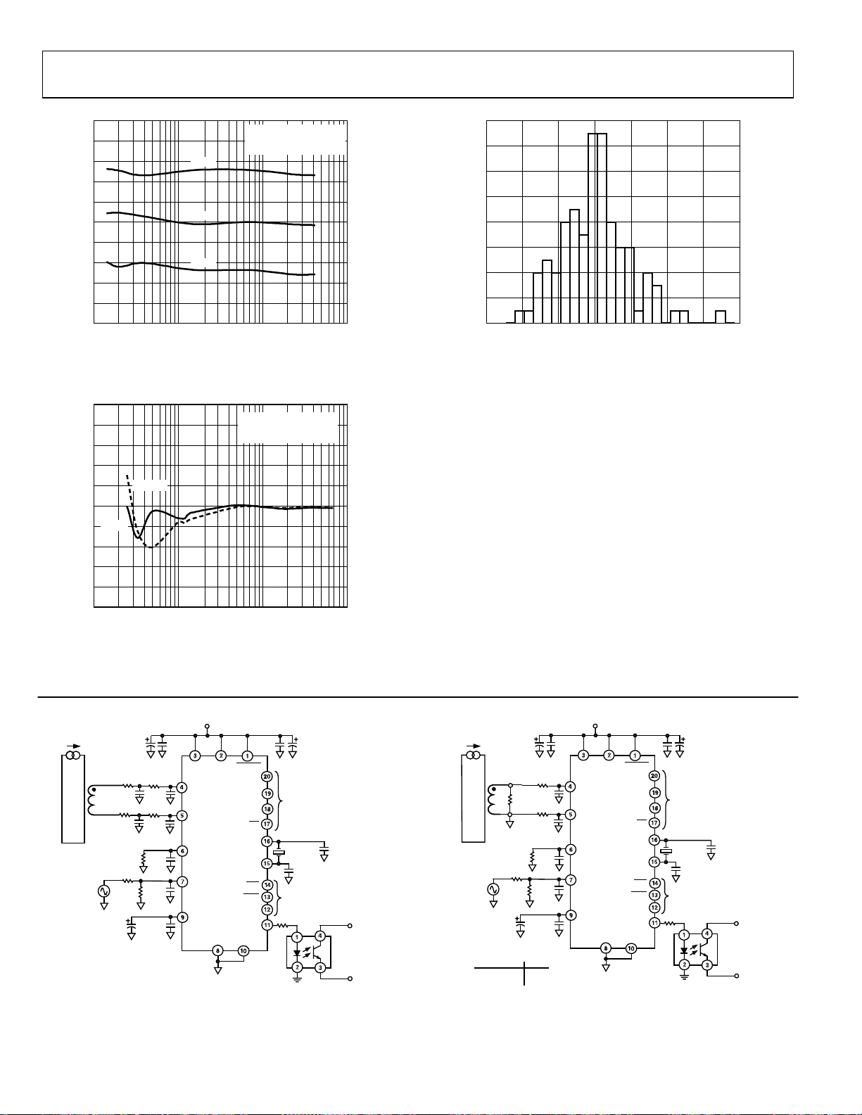
Figure 12. Active Energy Error as a Percentage of Reading (Gain = 8)
over Frequency with Internal Reference and Integrator Off
1.0
0.8
0.6
0.4
0.2
0
–0.2
ERROR (%)
–0.4
–0.6
–0.8
–1.0
0.1 101 100
PF = 1
PF = 0.5
FULL-SCALE CURRENT (%)
GAIN = 8
INTEGRATOR OFF
INTERNAL REFERENCE
Figure 13. IRMS Error as a Percentage of Reading (Gain = 8)
with Internal Reference and Integrator Off
0.5
0.4
0.3
0.2
0.1
0
–0.1
ERROR (%)
–0.2
–0.3
–0.4
–0.5
1 10 100
FULL-SCALE VOLTAGE (%)
GAIN = 1
EXTERNAL REFERENCE
Figure 14. VRMS Error as a Percentage of Reading (Gain = 1)
with External Reference
04481-A-012
04481-A-013
04481-A-020
1.0
0.8
GAIN = 8
INTEGRATOR ON
INTERNAL REFERENCE
0.6
0.4
0.2
0
–0.2
ERROR (%)
–0.4
–0.6
–0.8
–1.0
+25°C, PF = 0.5
0.1 101 100
FULL-SCALE CURRENT (%)
+85°C, PF = 0.5
+25°C, PF = 1
–40°C, PF = 0.5
Figure 15. Active Energy Error as a Percentage of Reading (Gain = 8)
over Power Factor with Internal Reference and Integrator On
1.0
0.8
GAIN = 8
INTEGRATOR ON
INTERNAL REFERENCE
0.6
0.4
0.2
0
–0.2
ERROR (%)
–0.4
–0.6
–0.8
–1.0
0.1 101 100
FULL-SCALE CURRENT (%)
+85°C, PF = 1
+25°C, PF = 1
–40°C, PF = 1
Figure 16. Active Energy Error as a Percentage of Reading (Gain = 8)
over Temperature with External Reference and Integrator On
3.0
2.5
2.0
1.5
1.0
0.5
0
ERROR (%)
–0.5
–1.0
–1.5
–2.0
45 47 49 51 53 55 57 59 61 63 65
PF = 0.5
PF = 1
FREQUENCY (Hz)
GAIN = 8
INTEGRATOR ON
INTERNAL REFERENCE
Figure 17. Active Energy Error as a Percentage of Reading (Gain = 8)
over Frequency with Internal Reference and Integrator On
04481-A-016
04481-A-015
04481-A-017
Rev. A | Page 11 of 56
ADE7763
0.5
0.4
0.3
5.25V
0.2
0.1
0
–0.1
ERROR (%)
–0.2
5.00V
4.75V
–0.3
–0.4
–0.5
0.1 101 100
FULL-SCALE CURRENT (%)
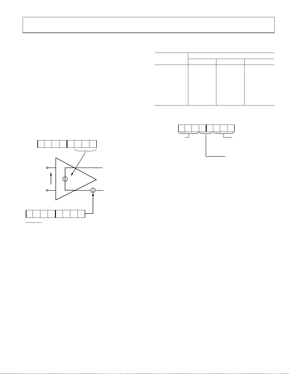
Figure 18. Active Energy Error as a Percentage of Reading (Gain = 8)
over Power Supply with Internal Reference and Integrator On
0.5
0.4
0.3
0.2
0.1
PF = 0.5
0
–0.1
ERROR (%)
PF = 1
–0.2
–0.3
–0.4
–0.5
0.1 101 100
FULL-SCALE CURRENT (%)
Figure 19. IRMS Error as a Percentage of Reading (Gain = 8)
with Internal Reference and Integrator On
GAIN = 8
INTEGRATOR ON
INTERNAL REFERENCE
GAIN = 8
INTEGRATOR ON
INTERNAL REFERENCE
16
14
12
10
8
HITS
6
4
2
0
–15 –10 –5 0 5 10 15 20
04481-A-081
CH1 OFFSET (0p5V_1X) (mV)
04481-A-021
Figure 20. Channel 1 Offset (Gain = 1)
04481-A-019
V
DD
100nF 100nF
AVDD DVDD
V1P
V1N
V2N
V2P
REF
U1
ADE7763
CLKOUT
IN/OUT
AGND DGND
RESET
DIN
DOUT
SCLK
CS
CLKIN
IRQ
SAG
ZX
CF
0
TOSPI BUS
(USED ONLY FOR
CALIBRATION)
22pF
U3
PS2501-1
22pF
TO
FREQUENCY
COUNTER
04481-A-023
Y1
3.58MHz
NOT CONNECTED
I
di/dt CURRENT
SENSOR
110V
CHANNEL 1 GAIN = 8
CHANNEL 2 GAIN = 1
10µF
100Ω 1kΩ
33nF 33nF
100Ω 1kΩ
33nF
1kΩ
600kΩ
1kΩ
10µF
V
DD
100nF 100nF
AVDD DVDD
V1P
33nF
V1N
ADE7763
V2N
V2P
REF
IN/OUT
AGND DGND
33nF
33nF
100nF
U1
RESET
DIN
DOUT
SCLK
CLKOUT
CLKIN
IRQ
SAG
CS
ZX
CF
10µF
TOSPI BUS
(USEDONLYFOR
CALIBRATION)
22pF
U3
PS2501-1
22pF
TO
FREQUENCY
COUNTER
Y1
3.58MHz
NOT CONNECTED
04481-A-022
Rev. A | Page 12 of 56
I
110V
10µF1µF
CURRENT
TRANSFORMER
CT TURN RATIO = 1800:1
CHANNEL 2 GAIN = 1
GAIN 1 (CH1)
RB
10µF
1
8
1kΩ
600kΩ
1kΩ
1kΩ
33nF
1kΩ
33nF
33nF
100nF
RB
10Ω
1.21Ω
33nF
Figure 22. Test Circuit for Performance Curves with Integrator Off
ADE7763
THEORY OF OPERATION
ANALOG INPUTS
The ADE7763 has two fully differential voltage input channels.
The maximum differential input voltage for input pairs V1P/V1N
and V2P/V2N is ±0.5 V. In addition, the maximum signal level
on analog inputs for V1P/V1N and V2P/V2N is ±0.5 V with
respect to AGND.
Each analog input channel has a programmable gain amplifier
(PGA) with possible gain selections of 1, 2, 4, 8, and 16. The
gain selections are made by writing to the gain register—see
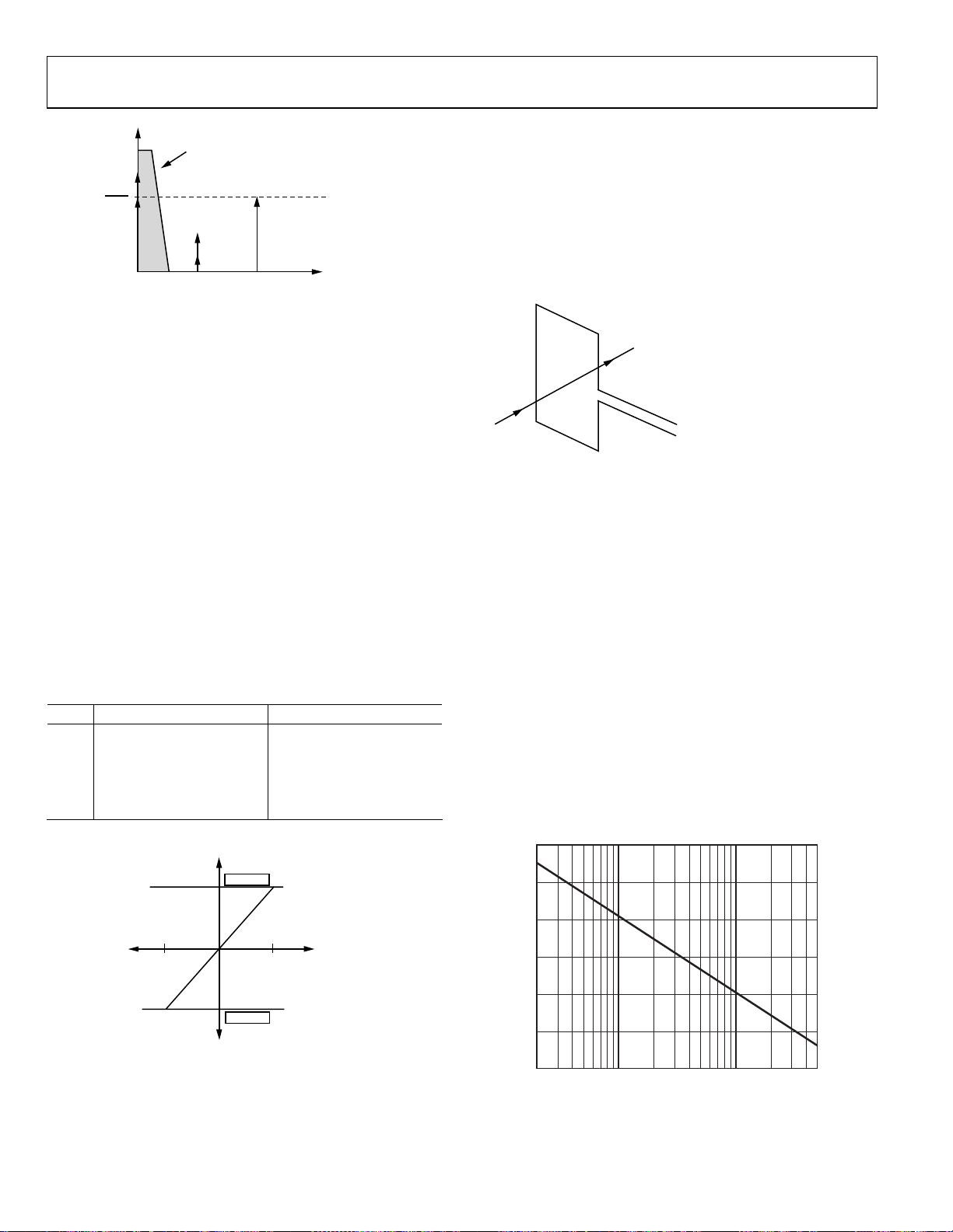
Figure 24. Bits 0 to 2 select the gain for the PGA in Channel 1;
the gain selection for the PGA in Channel 2 is made via Bits 5
to 7. Figure 23 shows how a gain selection for Channel 1 is
made using the gain register.
76 5 4 32 1 0
00 0 0 00 0 0
V1P
V
IN
V1N
76 5 4 32 1 0
00 0 0 00 0 0
CH1OS[7:0]
BITS 0 to 5: SIGN MAGNITUDE CODED OFFSET CORRECTION
BIT 6: NOT USED
BIT 7: DIGITAL INTEGRATOR (ON = 1, OFF = 0; DEFAULT OFF)
In addition to the PGA, Channel 1 also has a full-scale input
range selection for the ADC. The ADC analog input range
selection is also made using the gain register—see Figure 24. As
previously mentioned, the maximum differential input voltage
is 0.5 V. However, by using Bits 3 and 4 in the gain register, the
maximum ADC input voltage can be set to 0.5 V, 0.25 V, or
0.125 V. This is achieved by adjusting the ADC reference—see
the Reference Circuit section. Table 5 summarizes the
maximum differential input signal level on Channel 1 for the
various ADC range and gain selections.
GAIN[7:0]
GAIN (K)
SELECTION
K × V
IN
+
OFFSET ADJUST
(±50mV)
Figure 23. PGA in Channel 1
04481-A-024
Table 5. Maximum Input Signal Levels for Channel 1
Max Signal
Channel 1
0.5 V 0.25 V 0.125 V
ADC Input Range Selection
0.5 V Gain = 1 − −
0.25 V Gain = 2 Gain = 1 −
0.125 V Gain = 4 Gain = 2 Gain = 1
0.0625 V Gain = 8 Gain = 4 Gain = 2
0.0313 V Gain = 16 Gain = 8 Gain = 4
0.0156 V − Gain = 16 Gain = 8
0.00781 V − − Gain = 16
CHANNEL 1 AND CHANNEL 2 PGA CONTROL
PGA 2 GAIN SELECT
×
1
000 =
×
2
001 =
×
4
010 =
011 =
×
8
×
16
100 =
*REGISTER CONTENTS
7 6 5 4 3 2 1 0
0 0 0 0 0 0 0 0
SHOW POWER-ON DEFAULTS
GAIN REGISTER*
ADDR:
0x0A
PGA 1 GAIN SELECT
000 =
×
1
×
2
001 =
×
4
010 =
011 =
×
8
×
16
100 =
CHANNEL 1 FULL-SCALE SELECT
00 = 0.5V
01 = 0.25V
10 = 0.125V
Figure 24. Analog Gain Register
It is also possible to adjust offset errors on Channel 1 and
Channel 2 by writing to the offset correction registers (CH1OS
and CH2OS, respectively). These registers allow channel offsets
in the range ±20 mV to ±50 mV (depending on the gain setting)
to be removed. Note that it is not necessary to perform an offset
correction in an energy measurement application if HPF in
Channel 1 is switched on. Figure 25 shows the effect of offsets
on the real power calculation. As seen from Figure 25, an offset
on Channel 1 and Channel 2 contributes a dc component after
multiplication. Because this dc component is extracted by LPF2
to generate the active (real) power information, the offsets
contribute an error to the active power calculation. This problem
is easily avoided by enabling HPF in Channel 1. By removing
the offset from at least one channel, no error component is
generated at dc by the multiplication. Error terms at cos(
ωt) are
removed by LPF2 and by integration of the active power signal
in the active energy register (AENERGY[23:0])—see the Energy
Calculation section.
04481-A-025
Rev. A | Page 13 of 56
ADE7763
DC COMPONENT (INCLUDING ERROR TERM)
IS EXTRACTED BY THE LPF FOR REAL
× I
V
OS
OS
V × I
2
0
Figure 25. Effect of Channel Offsets on the Real Power Calculation
The contents of the offset correction registers are 6-bit, sign and
magnitude coded. The weight of the LSB depends on the gain
setting, i.e., 1, 2, 4, 8, or 16. Table 6 shows the correctable offset
span for each of the gain settings and the LSB weight (mV) for
the offset correction registers. The maximum value that can be
written to the offset correction registers is ±31d—see Figure 26.
Figure 26 shows the relationship between the offset correction
register contents and the offset (mV) on the analog inputs for a
gain of 1. To perform an offset adjustment, connect the analog
inputs to AGND; there should be no signal on either Channel 1
or Channel 2. A read from Channel 1 or Channel 2 using the
waveform register indicates the offset in the channel. This offset
can be canceled by writing an equal and opposite offset value to
the Channel 1 offset register, or an equal value to the Channel 2
offset register. The offset correction can be confirmed by
performing another read. Note that when adjusting the offset of
Channel 1, the digital integrator and the HPF should be
disabled.
Table 6. Offset Correction Range—Channels 1 and 2
Gain Correctable Span LSB Size
1 ±50 mV 1.61 mV/LSB
2 ±37 mV 1.19 mV/LSB
4 ±30 mV 0.97 mV/LSB
8 ±26 mV 0.84 mV/LSB
16 ±24 mV 0.77 mV/LSB
POWER CALCULATION
I
× V
OS
× I
V
OS
2ωω
FREQUENCY (RAD/S)
CH1OS[5:0]
04481-A-026
The current and voltage rms offsets can be adjusted with the
IRMSOS and VRMSOS registers—see the Channel 1 RMS Offset
Compensation and Channel 2 RMS Offset Compensation
sections.
di/dt CURRENT SENSOR AND DIGITAL INTEGRATOR
A di/dt sensor detects changes in magnetic field caused by ac
current. Figure 27 shows the principle of a di/dt current sensor.
MAGNETIC FIELD CREATED BY CURRENT
(DIRECTLY PROPORTIONAL TO CURRENT)
+ EMF (ELECTROMOTIVE FORCE)
– INDUCED BY CHANGES IN
MAGNETIC FLUX DENSITY (di/dt)
Figure 27. Principle of a di/dt Current Sensor
The flux density of a magnetic field induced by a current is
directly proportional to the magnitude of the current. Changes
in the magnetic flux density passing through a conductor loop
generate an electromotive force (EMF) between the two ends of
the loop. The EMF is a voltage signal that is proportional to the
di/dt of the current. The voltage output from the di/dt current
sensor is determined by the mutual inductance between the
current-carrying conductor and the di/dt sensor. The current
signal must be recovered from the di/dt signal before it can be
used. An integrator is therefore necessary to restore the signal to
its original form. The ADE7763 has a built-in digital integrator
to recover the current signal from the di/dt sensor. The digital
integrator on Channel 1 is switched off by default when the
ADE7763 is powered up. Setting the MSB of CH1OS register
turns on the integrator. Figure 28, Figure 29, Figure 30, and
Figure 31 show the magnitude and phase response of the digital
integrator.
10
04481-A-028
01,1111b
0x1F
0x00
0x3F
0mV
11,1111b
–50mV
Figure 26. Channel 1 Offset Correction Range (Gain = 1)
SIGN + 5 BITS
+50mV
OFFSET
ADJUST
SIGN + 5 BITS
0
–10
–20
GAIN (dB)
–30
04481-A-027
–40
–50
2
10
FREQUENCY (Hz)
3
10
04481-A-029
Figure 28. Combined Gain Response of the
Digital Integrator and Phase Compensator
Rev. A | Page 14 of 56
ADE7763
×1,×2,×
V
–88.0
–88.5
–89.0
–89.5
PHASE (Degrees)
–90.0
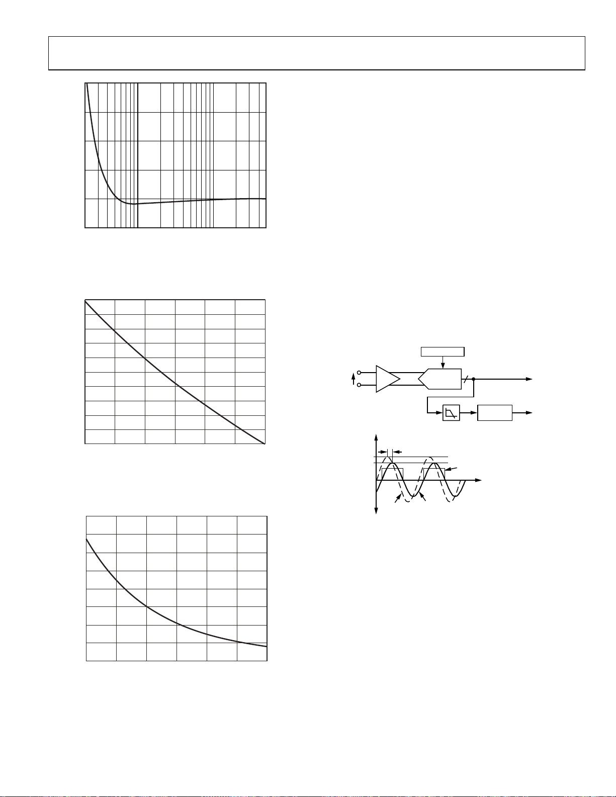
Note that the integrator has a –20 dB/dec attenuation and
approximately a –90° phase shift. When combined with a di/dt
sensor, the resulting magnitude and phase response should be a
flat gain over the frequency band of interest. The di/dt sensor
has a 20 dB/dec gain. It also generates significant high
frequency noise, necessitating a more effective antialiasing filter
to avoid noise due to aliasing—see the Antialias Filter section.
When the digital integrator is switched off, the ADE7763 can be
used directly with a conventional current sensor such as a current
transformer (CT) or with a low resistance current shunt.
–90.5
2
10
FREQUENCY (Hz)
3
10
Figure 29. Combined Phase Response of the
Digital Integrator and Phase Compensator
–1.0
–1.5
–2.0
–2.5
–3.0
–3.5
GAIN (dB)
–4.0
–4.5
–5.0
–5.5
–6.0
40 7045
50 55 60 65
FREQUENCY (Hz)
Figure 30. Combined Gain Response of the
Digital Integrator and Phase Compensator (40 Hz to 70 Hz)
–89.70
–89.75
–89.80
–89.85
–89.90
–89.95
PHASE (Degrees)
–90.00
–90.05
–90.10
40 45 7050 55 60 65
FREQUENCY (Hz)
Figure 31. Combined Phase Response of the
Digital Integrator and Phase Compensator (40 Hz to 70 Hz)
ZERO-CROSSING DETECTION
04481-A-030
04481-A-031
04481-A-032
The ADE7763 has a zero-crossing detection circuit on Channel 2.
This zero crossing is used to produce an external zero-crossing
signal (ZX), which is used in the calibration mode (see the
Calibrating an Energy Meter section). This signal is also used to
initiate a temperature measurement (see the Temperature
Measurement section).
Figure 32 shows how the zero-crossing signal is generated from
the output of LPF1.
1,
16
2.32° @ 60Hz
REFERENCE
ADC 2
LPF1
f
= 140Hz
–
3dB
LPF1
–63%TO +63% FS
1
CROSSING
ZX
ZERO
TO
MULTIPLIER
ZX
04481-A-033
×8,×
V2P
2
V2N
1.0
0.93
{GAIN[7:5]}
PGA2
V2
Figure 32. Zero-Crossing Detection on Channel 2
The ZX signal goes logic high upon a positive-going zero
crossing and logic low upon a negative-going zero crossing on
Channel 2. The ZX signal is generated from the output of LPF1.
LPF1 has a single pole at 140 Hz (@ CLKIN = 3.579545 MHz).
As a result, there is a phase lag between the analog input signal
V2 and the output of LPF1. The phase response of this filter is
shown in the Channel 2 Sampling section. The phase lag response
of LPF1 results in a time delay of approximately 1.14 ms
(@ 60 Hz) between the zero crossing on the analog inputs of
Channel 2 and the rising or falling edge of ZX.
Rev. A | Page 15 of 56

ADE7763
Zero-crossing detection also drives the ZX flag in the interrupt
status register. An active low in the
corresponding bit in the interrupt enable register is set to Logic 1.
The flag in the interrupt status register and the
set to their default values when reset (RSTSTATUS) is read in
the interrupt status register.
Zero-Crossing Timeout
Zero-crossing detection has an associated timeout register,
ZXTOUT. This unsigned, 12-bit register is decremented (1 LSB)
every 128/CLKIN seconds. The register is reset to its userprogrammed, full-scale value when a zero crossing on Channel 2
is detected. The default power-on value in this register is 0xFFF.
If the internal register decrements to 0 before a zero crossing is
detected and the DISSAG bit in the mode register is Logic 0, the
pin will go active low. The absence of a zero crossing is
SAG
also indicated on the
pin if the ZXTO enable bit in the
IRQ
interrupt enable register is set to Logic 1. Irrespective of the
enable bit setting, the ZXTO flag in the interrupt status register
is always set when the internal ZXTOUT register is
decremented to 0—see the Interrupts section.
The ZXOUT register, Address 0x1D, can be written to and read
from by the user—see the Serial Interface section. The
resolution of the register is 128/CLKIN seconds per LSB;
therefore, the maximum delay for an interrupt is 0.15 seconds
12
(128/CLKIN × 2
).
Figure 33 shows the zero-crossing timeout detection when the
line voltage stays at a fixed dc level for more than CLKIN/128 ×
ZXTOUT seconds.
12-BIT INTERNAL
REGISTER VALUE
ZXTOUT
output appears if the
IRQ
IRQ
output are
PERIOD MEASUREMENT
The ADE7763 provides the period measurement of the line.
The PERIOD register is an unsigned, 16-bit register that is
updated every period and always has an MSB of zero.
When CLKIN = 3.579545 MHz, the resolution of this register is
2.2 ms/LSB, which represents 0.013% when the line frequency is
60 Hz. When the line frequency is 60 Hz, the value of the
period register is approximately 7457d. The length of the register
enables the measurement of line frequencies as low as 13.9 Hz.
The period register is stable at ±1 LSB when the line is established
and the measurement does not change. This filter is associated
with a settling time of 1.8 seconds before the measurement is
stable. See the Calibrating an Energy Meter section for more on
the period register.
POWER SUPPLY MONITOR
The ADE7763 contains an on-chip power supply monitor. The
analog supply (AVDD) is continuously monitored. If the supply
is less than 4 V ± 5%, the ADE7763 will go into an inactive state
and no energy will accumulate. This is useful to ensure correct
device operation during power-up and power-down stages. In
addition, built-in hysteresis and filtering help prevent false
triggering due to noisy supplies.
AV
DD
5V
4V
0V
ADE7763
POWER-ON
INACTIVE
STATE
INACTIVE ACTIVE INACTIVE
TIME
CHANNEL 2
ZXTO
DETECTION
BIT
Figure 33. Zero-Crossing Timeout Detection
As seen in Figure 34, the trigger level is nominally set at 4 V.
The tolerance on this trigger level is about ±5%. The
can also be used as a power supply monitor input to the MCU.
04481-A-034
The
state. The power supply and decoupling for the part should be
such that the ripple at AVDD does not exceed 5 V ± 5%, as
specified for normal operation.
Rev. A | Page 16 of 56
SAG
Figure 34. On-Chip Power Supply Monitor
SAG
pin goes logic low when the ADE7763 is in its inactive
SAG
pin
04481-A-035
ADE7763
LINE VOLTAGE SAG DETECTION
In addition to detecting the loss of the line voltage when there
are no zero crossings on the voltage channel, the ADE7763 can
also be programmed to detect when the absolute value of the line
voltage drops below a peak value for a specified number of line
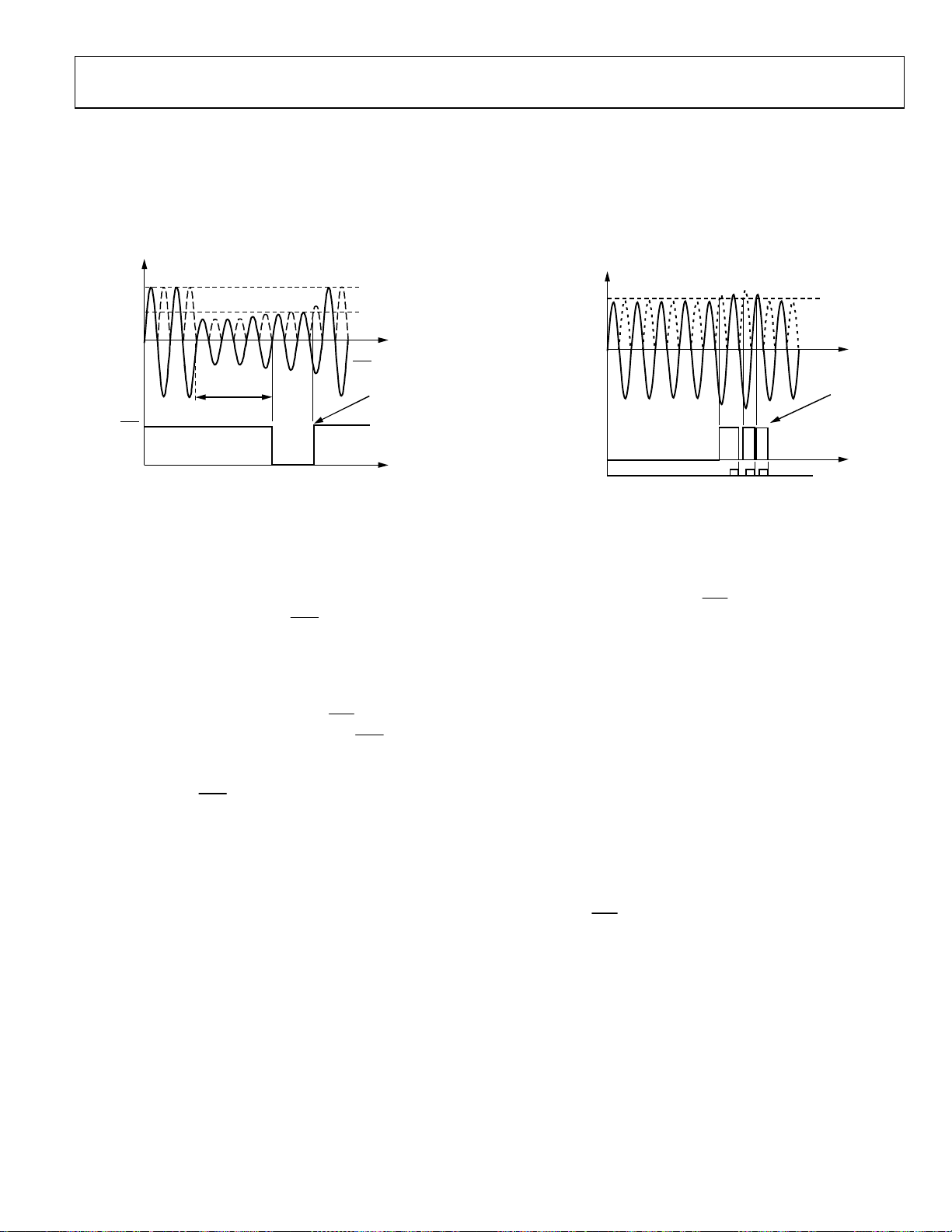
cycles. This condition is illustrated in Figure 35.
FULL SCALE
SAGLVL[7:0]
CHANNEL 2
PEAK DETECTION
The ADE7763 can also be programmed to detect when the
absolute value of the voltage or current channel exceeds a
specified peak value. Figure 36 illustrates the behavior of the
peak detection for the voltage channel.
Both Channel 1 and Channel 2 are monitored at the same time.
V
2
VPKLVL[7:0]
SAG RESET HIGH
WHEN CHANNEL 2
EXCEEDS SAGLVL[7:0]
SAGCYC[7:0] = 0x04
SAG
3 LINE CYCLES
Figure 35. Sag Detection
In Figure 35 the line voltage falls below a threshold that
has been set in the sag level register (SAGLVL[7:0]) for three
line cycles. The quantities 0 and 1 are not valid for the SAGCYC
register, and the contents represent one more than the desired
number of full line cycles. For example, if the DISSAG bit in the
mode register is Logic 0 and the sag cycle register
(SAGCYC[7:0]) contains 0x04, the
pin goes active low at
SAG
the end of the third line cycle for which the line voltage
(Channel 2 signal) falls below the threshold. As is the case when
zero crossings are no longer detected, the sag event is also
recorded by setting the SAG flag in the interrupt status register.
If the SAG enable bit is set to Logic 1, the
go active low—see the Interrupts section. The
logic output will
IRQ
pin goes
SAG
logic high again when the absolute value of the signal on Channel
2 exceeds the level set in the sag level register. This is shown in
Figure 35 when the
pin goes high again during the fifth line
SAG
cycle from the time when the signal on Channel 2 first dropped
below the threshold level.
Sag Level Set
The contents of the sag level register (1 byte) are compared to
the absolute value of the most significant byte output from
LPF1 after it is shifted left by one bit. For example, the nominal
maximum code from LPF1 with a full-scale signal on Channel 2
is 0x2518—see the Channel 2 Sampling section. Shifting one bit
left gives 0x4A30. Therefore, writing 0x4A to the SAG level
register puts the sag detection level at full scale. Writing 0x00 or
0x01 puts the sag detection level at 0. The SAG level register is
compared to the most significant byte of a waveform sample
after the shift left, and detection occurs when the contents of
the sag level register are greater.
PKV RESET LOW
WHEN RSTSTATUS
REGISTER IS READ
PKV INTERRUPT
FLAG (BIT 8 OF
STATUS REGISTER)
04481-A-036
READ RSTSTATUS
REGISTER
Figure 36. Peak Level Detection
04481-A-037
Figure 36 shows a line voltage exceeding a threshold that has
been set in the voltage peak register (VPKLVL[7:0]). The
voltage peak event is recorded by setting the PKV flag in the
interrupt status register. If the PKV enable bit is set to Logic 1 in
the interrupt mask register, the
logic output will go active
IRQ
low. Similarly, the current peak event is recorded by setting the
PKI flag in the interrupt status register—see the Interrupts
section.
Peak Level Set
The contents of the VPKLVL and IPKLVL registers are
compared to the absolute value of Channel 1 and Channel 2,
respectively, after they are multiplied by 2. For example, the
nominal maximum code from the Channel 1 ADC with a fullscale signal is 0x2851EC—see the Channel 1 Sampling section.
Multiplying by 2 gives 0x50A3D8. Therefore, writing 0x50 to
the IPKLVL register, for example, puts the Channel 1 peak
detection level at full scale and sets the current peak detection
to its least sensitive value. Writing 0x00 puts the Channel 1
detection level at 0. Peak level detection is done by comparing
the contents of the IPKLVL register to the incoming Channel 1
sample. The
pin indicates that the peak level is exceeded if
IRQ
the PKI or PKV bits are set in the interrupt enable register
(IRQEN [15:0]) at Address 0x0A.
Peak Level Record
The ADE7763 records the maximum absolute value reached by
Channel 1 and Channel 2 in two different registers—IPEAK
and VPEAK, respectively. VPEAK and IPEAK are 24-bit,
unsigned registers. These registers are updated each time the
absolute value of the waveform sample from the corresponding
channel is above the value stored in the VPEAK or IPEAK
register. The contents of the VPEAK register correspond to two
Rev. A | Page 17 of 56
 Loading...