PRELIMINARY TECHNICAL DATA
Evaluation Board Documentation
=
Preliminary Technical Data
FEATURES
Evaluation Board is designed to be used together with
accompanying software to implement a fully functional
Energy Meter (Watt-Hour Meter).
Easy connection of various external transducers via
screw terminals.
Easy modification of signal conditioning components
using PCB sockets.
LED indicators on logic outputs CF, ZX, SAG and IRQ.
Optically isolated data output connection to PC parallel port.
Optically isolated frequency output (CF) to BNC.
External Reference option available for
on-chip reference evaluation.
GENERAL DESCRIPTIONGENERAL DESCRIPTION
GENERAL DESCRIPTION
GENERAL DESCRIPTIONGENERAL DESCRIPTION
The ADE7756 is a high accuracy electrical power measurement IC with a serial interface and a pulse output.
The ADE7756 incorporates two second order sigma delta
ADCs, reference circuitry, temperature sensor and all the
signal processing required to perform active power and
energy measurement.
This documentation describes the ADE7756 evaluation kit
Hardware and Software functionality. The ADE7756
AD7756 Energy metering IC
EVAL-ADE7756EB
evaluation board, together with the ADE7756 data sheet
and this documentation provides a complete evaluation
platform for the ADE7756.
The evaluation board has been designed so that the
ADE7756 can be evaluated in the end application, i.e.,
Watt-Hour Meter. Using the appropriate transducers on
the current channel (e.g., shunt, CT etc.) the evaluation
board can be connected to a test bench or high voltage
(240V rms) test circuit. An on-board resistor divider
network provides the attenuation for the line voltage. This
application note also describes how the current transducers
should be connected for the best performance.
The evaluation board (watt-hour meter) is configured and
calibrated via the parallel port of a PC. The data interface
between the evaluation board and the PC is fully isolated.
Windows
board which allows it to be quickly configured as an
energy meter.
The evaluation board also functions as a stand alone
evaluation system which can be easily incorporated into an
existing system via a 25 way D-Sub connector.
The evaluation board requires two external 5V power
supplies (one is required for isolation purposes) and the
appropriate current transducer.
TM
based software is provided with the evaluation
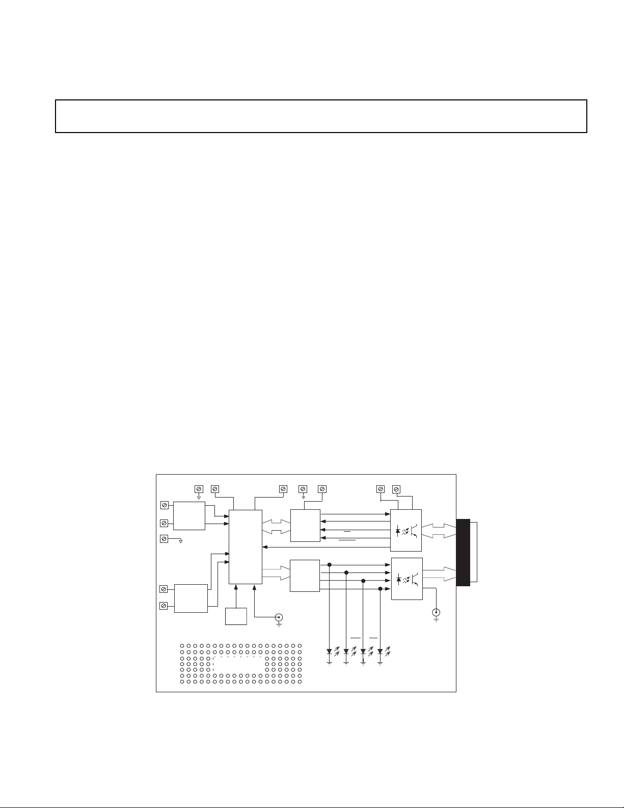
FUNCTIONAL BLOCK DIAGRAM
V1P
V1N
AGND
V2N
V2P
AGND
Filter
Network
Filter
Network
&
Attenuation
Optional External
2.5V Reference
AV
DD
ADE7756
AD780
PROTOTYPE
AREA
DV
DD
BNC
External
Clock in
DGND
74HC08
74HC08
REV. PrB 01/01
Information furnished by Analog Devices is believed to be accurate and
reliable. However, no responsibility is assumed by Analog Devices for its
use, nor for any infringements of patents or other rights of third parties
which may result from its use. No license is granted by implication or
otherwise under any patent or patent rights of Analog Devices.
+5V
DOUT
SCLK
DIN
CS
RESET
CF ZX
SAG
One Technology Way, P.O. Box 9106, Norwood. MA 02062-9106, U.S.A.
Tel: 617/329-4700 Fax: 617/326-8703
V+
Isolated Frequency
IRQ
V-
Connector to
PC Parallel
Port
BNC
CF
output
EVAL-ADE7756EB
PRELIMINARY TECHNICAL DATA
PRELIMINARY TECHNICAL DATA
ANALOG INPUTS (SK1 AND SK2)ANALOG INPUTS (SK1 AND SK2)
ANALOG INPUTS (SK1 AND SK2)
ANALOG INPUTS (SK1 AND SK2)ANALOG INPUTS (SK1 AND SK2)
Voltage and current signals are connected at the screw terminals SK1 and SK2 respectively. All analog input signals are
filtered using the on-board anti-alias filters before being
presented to the analog inputs of the ADE7756. The
default component values which are shipped with the
evaluation board are the recommended values to be used
with the ADE7756. The user can easily change these
components, however this is not recommended unless the
user is familiar with sigma-delta converters and also the
criteria used for selecting the component values for the
analog input filters—see AN-559 for a more comprehensive description of the anti-alias filters and their function.
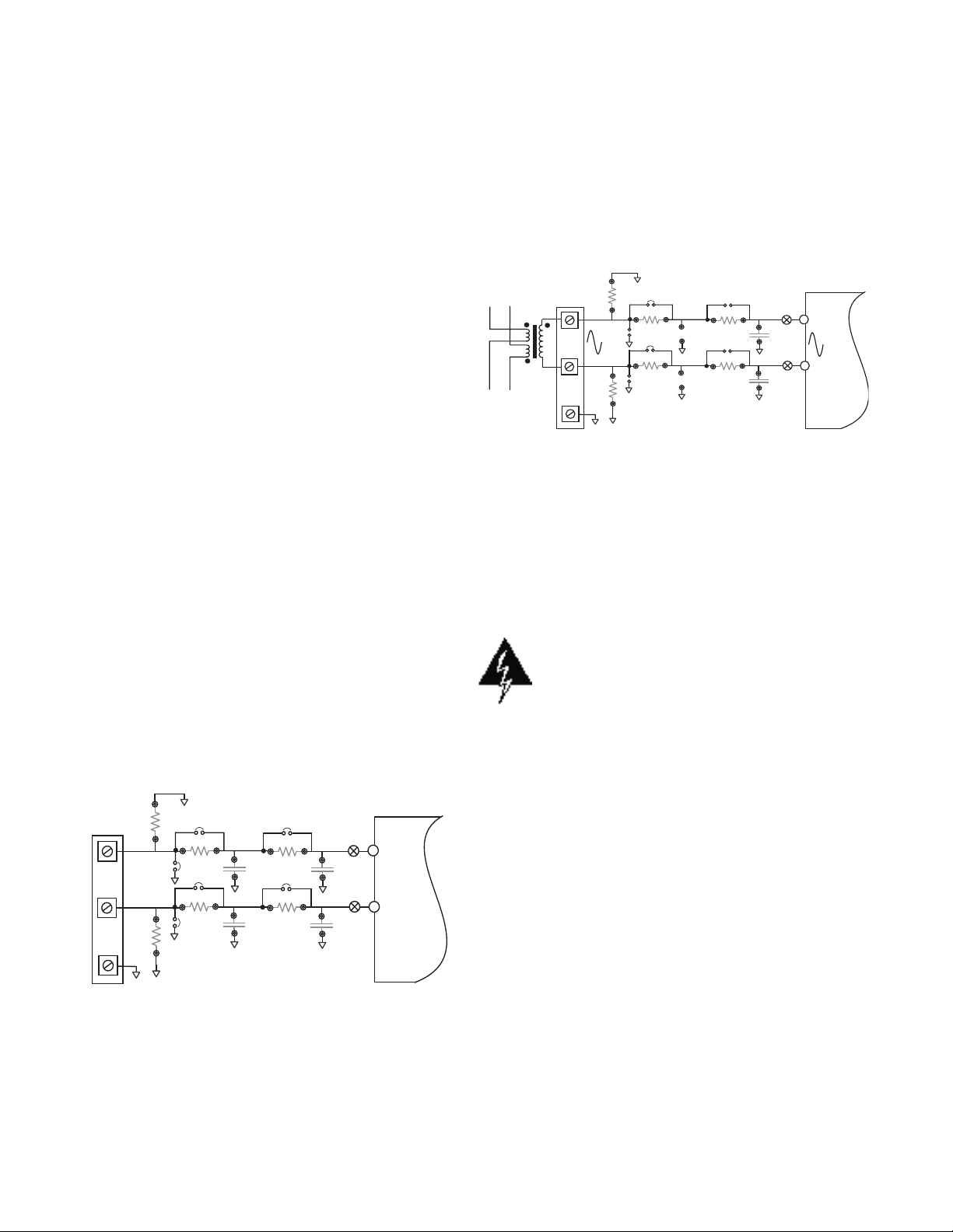
Current sense inputs (SK2)
SK2 is a three-way connection block which allows the
ADE7756 to be connected to a current transducer. Figure
1 shows the connector SK2 and the filtering network
which is provided on the evaluation board.
The resistors SH1A and SH1B are by default not populated. They are intended to be used as burden resistors
when a CT is used as the current transducer—see using a
CT as a the current transducer.
The RC networks R41/C11 and R42/C21 are used to
provide phase compensation when a shunt is being used as
the current transducer—see using a shunt as the current
transducer. These RC networks are easily disabled by
placing JP15 & JP25 and removing C11 & C21 (socketed).
The RC networks R50/C50 & R51/C51 are the anti-alias
filters which are required by the on-chip ADCs. The
default corner frequency for these LPFs (Low Pass
Filters) is selected as 4.8kHz (1kΩ & 33nF). These filters
can easily be adjusted by replacing the components on the
evaluation board. However before adjusting the component values of R50, R51, C50 or C51 the user should first
review application note AN-559.
ADE7756
JP2
JP15
R41
100Ω
JP25
R42
100Ω
JP4
SH1A
SK2 1
SK2 2
SH1B
SK2 3
Figure 1 — Current Channel on the ADE7756 evaluation
C11
33nF
C21
33nF
board
JP1
R50
1kΩ
JP3
R51
1kΩ
TP1
C50
33nF
C51
33nF
V1P
TP2
V1N
Using a CT as the current transducer
Figure 2 shows how a CT can be used as a current
transducer in a signal phase 3-wire distribution system.
This is how electrical energy is distributed to residential
users in the United States. Phase A and Phase B are
nominally 180° out of phase. The vector addition of the
two currents is easily achieved by using two primary turns
of opposite polarity on the CT.
33nF
33nF
TP1
TP2
ADE7756
V1P
355mV
rms
V1N
Phase A
I max = 80A
CT
1:1800
Phase B
SH1A
SH1B
JP15
4Ω
100Ω
JP2
JP25
100Ω
JP4
4Ω
JP1
1kΩ
JP3
1kΩ
Full Scale
differential input = 1V
Gain = 2
Figure 2 — CT connection to Current Channel
The CT secondary current is converted to a voltage by
using a burden resistance across the secondary winding
outputs. Care should be taken when using a CT as the
current transducer. If the secondary is left open, i.e., no
burden is connected, a large voltage could be present at
the secondary outputs. This can cause an electrical shock
hazard and potentially damage electronic components.
Warning!
Using a CT without a burden resistor
can lead to electrical shock.
When using a CT as the current sensor, the phase compensation network for a shunt application should be
disabled. This is achieved by closing jumpers JP15/JP25
and removing C11/C21.
The anti-alias filters should be enabled by opening
jumpers JP1/JP3—see Figure 2.
Most CTs will have an associated phase shift of between
0.1° and 1° at 50Hz/60Hz. This phase shift or phase error
can lead to significant energy measurement errors, especially at low power factors—see AN-559 for more information. However this phase error can be corrected by
writing to the Phase Calibration register (PHCAL) in the
ADE7756. The software supplied with the ADE7756
evaluation board allows user adjustment of the Phase
Calibration register. See the Evaluation Software Description
for more information.
For this example, notice that the maximum analog input
range on Channel 1 is set to 1V. And the Gain for Channel 1 has be set to 2. The maximum analog input range
and gain are set via the Gain register (GAIN)—see the
ADE7756 data sheet. The evaluation software allows the
user to configure the channel range and gain. This means
that the maximum peak differential signal on Channel 1 is
0.5V.
–2–
REV. PrB 01/01
PRELIMINARY TECHNICAL DATA
PRELIMINARY TECHNICAL DATA
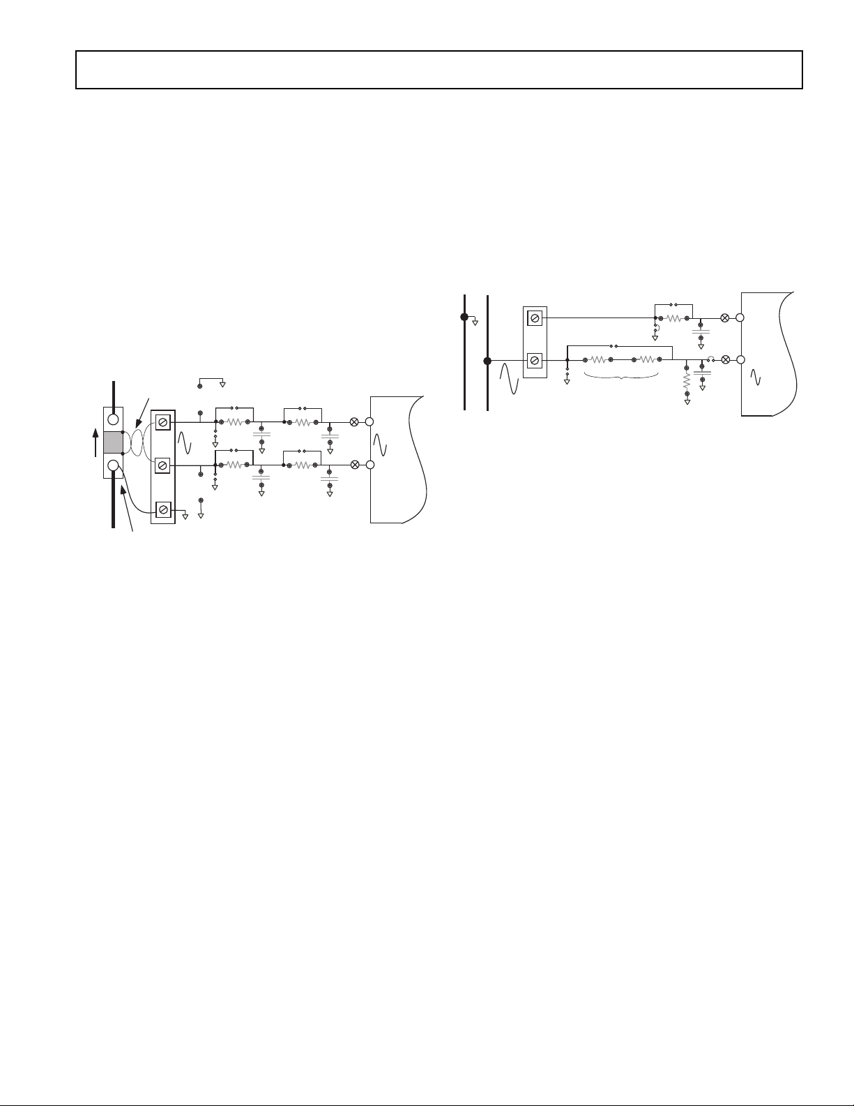
Using a shunt resistor as the current transducer
Figure 3 shows how a shunt resistance can be used to
perform the current to voltage conversion required for the
ADE7756. A shunt is a very cost effective way to perform
the current to voltage conversion in a two-wire, singlephase application. No isolation is required in a two-wire
application and the shunt has advantages over the CT
arrangement. For example a shunt does not suffer from dc
saturation problems and the phase response of the shunt is
linear over a very wide dynamic range. Although the shunt
is predominately resistive, it does have parasitic reactive
elements (inductance) which can become significant, even
at 50Hz/60Hz. This means that there can be a small phase
shift associated with the shunt. However once it is understood the phase shift is easily compensated with the filter
network R41/C11 and R42/C21—see AN-559 for a
detailed discussion of this issue.
Twisted pair
connection
200µΩ
80A
BVM-D-R0002-5.0
JP2
JP15
100Ω
JP25
100Ω
JP4
JP1
1kΩ
33nF
JP3
1kΩ
33nF
Full Scale
differential input = 0.5V
Gain = 16
Figure 3 — Shunt connection to Current Channel
The shunt used in this example is a 200µΩ manganin type.
The resistance of the shunt should be as low as possible in
order to avoid excessive power dissipation in the shunt.
Although the shunt is fabricated from a special alloy
(manganin) which has a very low temperature coefficient
of resistance, excessive heating due to power dissipation
can cause measurement inaccuracies when operating at
heavy loads over extended periods of time.
The manganin shunt used in this example (BVM-DR0002-5.0) is designed specifically for energy metering
applications and is supplied by Isotek Corp.
(http://www.isotekcorp.com).
This shunt is PCB mountable with a current carrying
ability of 70A rms. The technical data supplied by Isotek
Corp. gives detailed information regarding PCB layout.
Figure 3 shows how the shunt can be connected to the
evaluation board. Two sense wired should be soldered to
the shunt at the copper/manganium junctions as shown.
These sense wires should be formed into a twisted pair to
reduce the loop area which will reduce antenna effects. A
connection for the common mode voltage can be made at
the connection point for the current carrying conductor—
see Figure 3.
TP1
33nF
TP2
33nF
ADE7756
V1P
16mV
rms
V1N
EVAL-ADE7756EB
Voltage sense inputs
The voltage input connections on the ADE7756 evaluation board can be directly connected to the line voltage
source. The line voltage is attenuated using a simple
resistor divider network before it is presented to the
ADE7756. Because of the relatively large signal on this
channel and the small dynamic range requirement, the
voltage channel can be configured in a single-ended
configuration. Figure 4 shows a typical connection for the
line voltage.
C54
33nF
JP51
C53
33nF
ADE7756
TP5
V2N
TP4
V2P
200 - 300 mV
rms
JP9
JP10
255kΩ
R54
R57
1kΩ
JP3
R56
1kΩ
Neutral
Phase
SK1 1
SK1 2
100 - 250 V rms
JP8
R53
255kΩ
Attenuation
JP7
Network
Figure 4 — Voltage Channel on the ADE7756 evaluation
board
Note that the analog inputs V2N is connected to AGND
via the anti-alias filter R57/C54 using JP10. Jumper JP9
should be left open.
The voltage attenuation network is made up of R53, R54
and R56. The maximum signal level permissible at V2P is
1V peak. Although the ADE7756 analog inputs can
withstand ±6V without risk of permanent damage, the
signal range should not exceed ±1V with respect to
AGND, for specified operation.
The attenuation network can be easily modified by the
user to accommodate any input signal levels. However the
value of R56 (1kΩ) should not be altered as the phase
response of Channel 2 should match that of Channel 1—
see AN-559 (Attenuation Network).
REV. PrB 01/01
–3–
PRELIMINARY TECHNICAL DATA
EVAL-ADE7756EB
JUMPER SETTINGS
JUMEPER OPTION DESCRIPTION
JP1 Closed This will short out R50. The effect is to disable the anti-alias filter on the
analog input V1P. Default Open.
Open Enable the anti-alias filter on V1P.
JP2 Closed This will connect the analog input V1P to ground. Default Open.
JP3 Closed This will short out R51. The effect is to disable the anti-alias filter on the
analog input V1N. Default Open.
Open Enabe the anti-alias filter on V1N.
JP4 Closed This will connect the analog input V1N to ground. Default Open.
JP 5 A This connects the buffered logic output
IRQ to the LED1.
B This connects the buffered logic output
via an optical isolator.
JP 6 A This connects the buffered logic output
B This connects the buffered logic output
via an optical isolator.
JP7 Closed This will short the attenuation network on Channel 2. Default open.
JP8 Closed This will connect the analog input V2P to ground. Default Open.
JP9 Closed This will short out R57. The effect is to disable the anti-alias filter on the
analog input V2N. Default Open.
Open Enable the anti-alias filter on V2N.
JP10 Closed This will connect the analog input V2N to ground. Default Open.
JP11 Closed This will connect the Analog and Digital ground planes of the PCB. Default
Closed.
JP12 A This connects the buffered logic output CF to the LED4.
B This connects the buffered logic output CF to BNC2 connector via an optical
isolator.
JP13 Closed This will connect an external reference 2.5V (AD780) to the ADE7756.
Open This will enable the ADE7756 on-chip reference.
JP14 Closed This will connect the optical isolator ground to the evaluation board gound
(DGND). If full isolation between the evaluation board and PC is required,
this jumper should be left open.
IRQ to pin 10 on the D-Sub connector
SAG to the LED2.
SAG to pin 11 on the D-Sub connector
JP15 Closed This will short out R41. The effect is to disable the phase compensation filter
(for shunts) on the analog input V1P. Default Closed.
JP19 A This connects the buffered logic output ZX to the LED3.
B This connects the buffered logic output ZX to pin 12 on the D-Sub connector
via an optical isolator.
JP20 Closed This connects the AVDD and DVDD supply for the evaluation board together.
Default Closed.
JP21 Closed This connects the DVDD and +5V (buffers) supply for the evaluation board
together. Default Closed.
JP25 Closed This will short out R42. The effect is to disable the phase compensation filter
(for shunts) on the analog input V1N. Default Closed.
JP51 Closed This will short out disconnect Analog input V2P from the ADE7756. Default
Closed.
–4–
REV. PrB 01/01
PRELIMINARY TECHNICAL DATA
PRELIMINARY TECHNICAL DATA
JP20
JP1
JP15
JP2
JP4
JP10
JP7
JP8
JP25
JP9
JP51
JP3
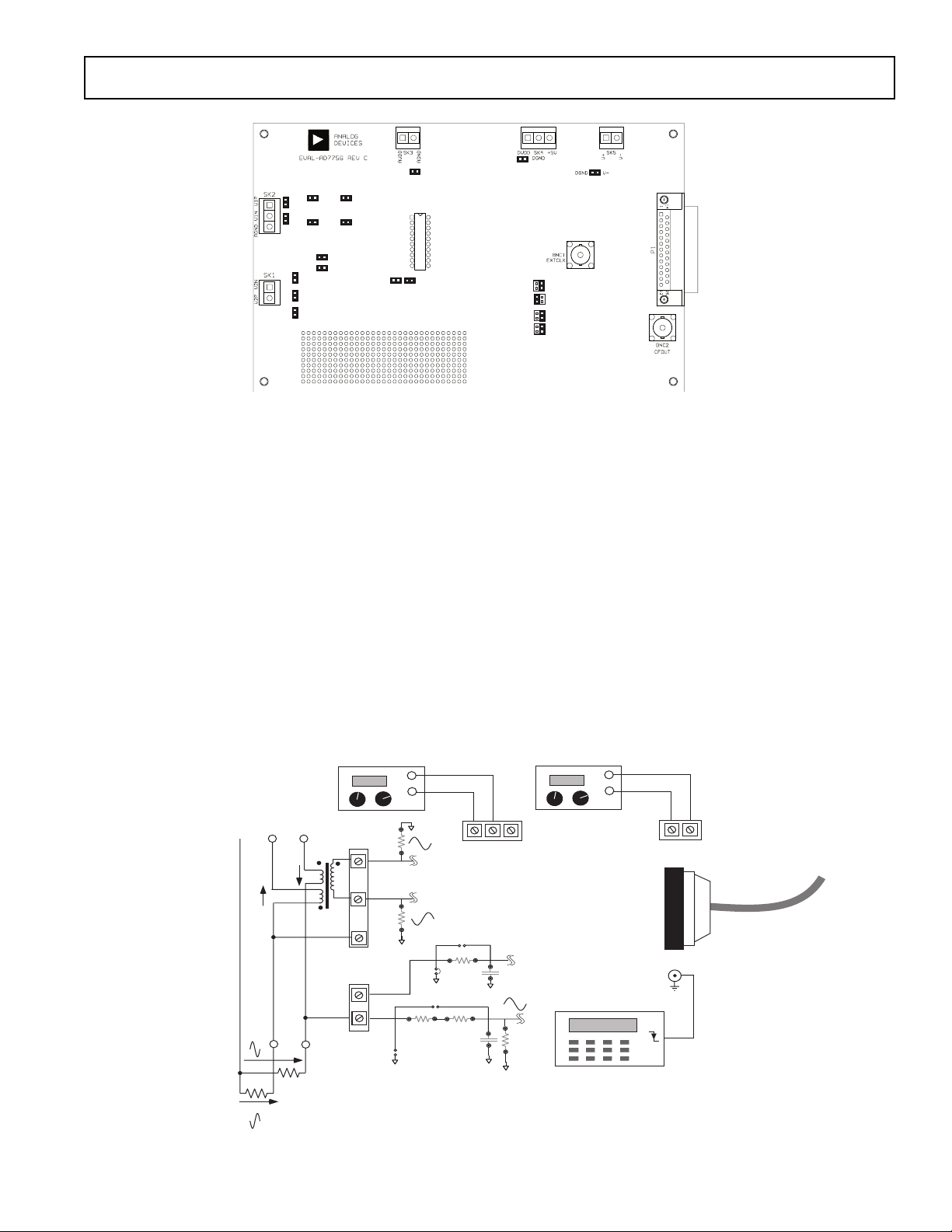
Figure 5 - ADE7756 evaluation board jumper positions
SETTING UP THE ADE7756 EVALUATION BOARDSETTING UP THE ADE7756 EVALUATION BOARD
SETTING UP THE ADE7756 EVALUATION BOARD
SETTING UP THE ADE7756 EVALUATION BOARDSETTING UP THE ADE7756 EVALUATION BOARD
Shown below is a typical set up for the ADE7756 evaluation board. In this example a kWh meter for a 3 wire,
single phase distribution system is shown. For a more
detailed description on how to use a CT as a current
transducer see the Current Sense Inputs section of this documentation. The line voltage is connected directly to the
evaluation board as shown. Note JP7 should be left open
to ensure that the attenuation network is not bypassed.
Also note the use of two power supplies. The second
power supply is used to power the optical isolation. With
JP14 left open, this will ensure that there is no electrical
connection between the high voltage test circuit and the
PC. The power supplies should have floating voltage
outputs.
JP13
AD7756
JP11
EVAL-ADE7756EB
JP21
AB
JP5
JP6
JP19
JP12
AB
The evaluation board is connected to the PC parallel port
using the cable supplied. The cable length should not
exceed 6 feets (2 meters) or the serial communication
between the PC and the evaluation board may become
unpredictable and error prone.
When the evaluation board has been powered up and is
connected to the PC, the supplied software can be
launched. The software will automatically start in energy
meter mode. The next section describes the ADE7756
evaluation software in detail and how it can be installed
and uninstalled.
JP14
REV. PrB 01/01
Neutral
110V
Load
110V
5.000 V
-
+
JP13 = Open
JP14 = Open
JP15 = Closed
JP19 = B
JP20 = Closed
JP21 = Closed
JP25 = Closed
1.0666 Hz
Phase B
110V
10A
10A
Load
Phase A
1:2000
CT
AGND
220V
5.000 V
SK2
SK1
2.5Ω
SH1A
SH1B
2.5Ω
-
+
25mV
R53
255kΩ 255kΩ
JP8
V1P
V1N
25mV
JP7
JP10
DVDD
JP1 = Open
JP2 = Open
JP3 = Open
JP4 = Open
JP5 = B
JP6 = B
JP9
R57
1kΩ
R54
C53
33nF
DGND
SK4
C54
33nF
450mV
+5V
1kΩ
JP7 = Open
JP8 = Open
JP9 = Open
JP10 = Closed
JP11 = Closed
JP12 = B
V2N
V2P
Figure 6 - Typical set up for the ADE7756 evaluation board
–5–
V+ V-
SK5
BNC2
To PC
Parallel Port
 Loading...