Polyphase Multifunction
Energy Metering IC with Serial Port
FEATURES
High Accuracy, Supports IEC 687/61036
Compatible with 3-Phase/3-Wire, 3-Phase/4-Wire
and any Type of 3-Phase Services
Less than 0.1% Error in Active Power Measurement over a
Dynamic Range of 1000 to 1
Supplies Active Energy, Apparent Energy, Voltage RMS,
Current RMS, and Sampled Waveform Data
Digital Power, Phase, and Input Offset Calibration
On-Chip Temperature Sensor (4C Typical after Calibration)
On-Chip User Programmable Thresholds for Line Voltage
SAG and Overdrive Detections
SPI Compatible Serial Interface with Interrupt
Request Line (IRQ)
Pulse Output with Programmable Frequency
Proprietary ADCs and DSP Provide High Accuracy over
Large Variations in Environmental Conditions and Time
Single 5 V Supply
GENERAL DESCRIPTION
The ADE7754 is a high accuracy polyphase electrical energy
measurement IC with a serial interface and a pulse output. The
ADE7754 incorporates second order Σ-∆ ADCs, reference
circuitry, temperature sensor, and all the signal processing
required to perform active, apparent energy measurements, and
rms calculation.
The ADE7754 provides different solutions for measuring active
and apparent energy from the six analog inputs, thus enabling
ADE7754
*
the use of the ADE7754 in various power meter services such as
3-phase/4-wire, 3-phase/3-wire, and 4-wire delta.
In addition to rms calculation, active and apparent power information, the ADE7754 provides system calibration features for
each phase (i.e., channel offset correction, phase calibration,
and gain calibration). The CF logic output provides instantaneous active power information.
The ADE7754 has a waveform sample register that enables
access to ADC outputs. The part also incorporates a detection
circuit for short duration low or high voltage variations. The
voltage threshold levels and the duration (number of half line
cycles) of the variation are user programmable.
A zero-crossing detection is synchronized with the zero-crossing
point of the line voltage of each of the three phases. The information collected is used to measure each line’s period. It is also
used internally to the chip in the line active energy and line
apparent energy accumulation modes. This permits faster and
more accurate calibration of the power calculations. This signal
is also useful for synchronization of relay switching.
Data is read from the ADE7754 via the SPI serial interface. The
interrupt request output (IRQ) is an open-drain, active low
logic output. The IRQ output goes active low when one or more
interrupt events have occurred in the ADE7754. A status register indicates the nature of the interrupt.
The ADE7754 is available in a 24-lead SOIC package.
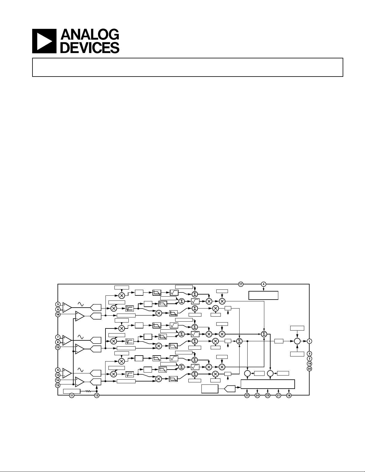
FUNCTIONAL BLOCK DIAGRAM
AVGAIN
PGA1
I
AP
I
AN
V
AP
I
BP
I
BN
V
BP
I
CP
I
CN
V
CP
V
N
PGA1
PGA1
2.4V REF
AGND
PGA2
PGA2
PGA2
4k
REF
ADC
ADC
ADC
ADC
ADC
ADC
AAPGAIN
APHCAL
BVGAIN
BAPGAIN
BPHCAL
CVGAIN
CAPGAIN
CPHCAL
IN/OUT
HPF
HPF
HPF
2
X
2
X
2
X
2
X
2
X
2
X
AVRMSOS
AIRMSOS
LPF2
BVRMSOS
BIRMSOS
LPF2
CVRMSOS
CIRMSOS
LPF2
REV. 0 *Patents pending.
Information furnished by Analog Devices is believed to be accurate and
reliable. However, no responsibility is assumed by Analog Devices for its
use, nor for any infringements of patents or other rights of third parties that
may result from its use. No license is granted by implication or otherwise
under any patent or patent rights of Analog Devices. Trademarks and
registered trademarks are the property of their respective companies.
AV
DD
POWER SUPPLY
MONITOR
DFC
SCLK
VADIV
%
CS
WDIV
%
ADE7754 REGISTERS AND
SERIAL INTERFACE
DOUT
DIN
ADE7754
CFNUM
CFDEN
IRQ
CF
DV
DD
DGND
CLKIN
CLKOUT
AAPOS
BAPOS
CAPOS
AWG
BWG
CWG
TEMP
SENSOR
RESET
AVAG
|X|
ABS
BVAG
|X|
ABS
CVAG
|X|
ABS
ADC
One Technology Way, P.O. Box 9106, Norwood, MA 02062-9106, U.S.A.
Tel: 781/329-4700 www.analog.com
Fax: 781/326-8703 © 2003 Analog Devices, Inc. All rights reserved.

ADE7754
Contents
GENERAL DESCRIPTION . . . . . . . . . . . . . . . . . . . . . . . . . 1
FEATURES . . . . . . . . . . . . . . . . . . . . . . . . . . . . . . . . . . . . . 1
SPECIFICATIONS . . . . . . . . . . . . . . . . . . . . . . . . . . . . . . . 3
TIMING CHARACTERISTICS . . . . . . . . . . . . . . . . . . . . . 4
ABSOLUTE MAXIMUM RATINGS . . . . . . . . . . . . . . . . . 5
ORDERING GUIDE . . . . . . . . . . . . . . . . . . . . . . . . . . . . . . 5
PIN CONFIGURATION . . . . . . . . . . . . . . . . . . . . . . . . . . . 5
PIN FUNCTION DESCRIPTIONS . . . . . . . . . . . . . . . . . . 5
TYPICAL PERFORMANCE CHARACTERISTICS . . . . . 7
TERMINOLOGY . . . . . . . . . . . . . . . . . . . . . . . . . . . . . . . . . 9
Measurement Error . . . . . . . . . . . . . . . . . . . . . . . . . . . . . . 9
Phase Error Between Channels . . . . . . . . . . . . . . . . . . . . . 9
Power Supply Rejection . . . . . . . . . . . . . . . . . . . . . . . . . . . 9
ADC Offset Error . . . . . . . . . . . . . . . . . . . . . . . . . . . . . . . 9
Gain Error . . . . . . . . . . . . . . . . . . . . . . . . . . . . . . . . . . . . . 9
Gain Error Match . . . . . . . . . . . . . . . . . . . . . . . . . . . . . . . 9
POWER SUPPLY MONITOR . . . . . . . . . . . . . . . . . . . . . . . 9
ANALOG INPUTS . . . . . . . . . . . . . . . . . . . . . . . . . . . . . . . 9
ANALOG-TO-DIGITAL CONVERSION . . . . . . . . . . . . . 10
Antialias Filter . . . . . . . . . . . . . . . . . . . . . . . . . . . . . . . . . 10
CURRENT CHANNEL ADC . . . . . . . . . . . . . . . . . . . . . . 11
Current Channel ADC Gain Adjust . . . . . . . . . . . . . . . . . 11
Current Channel Sampling . . . . . . . . . . . . . . . . . . . . . . . 11
VOLTAGE CHANNEL ADC . . . . . . . . . . . . . . . . . . . . . . 12
ZERO-CROSSING DETECTION . . . . . . . . . . . . . . . . . . . 12
Zero-Crossing Timeout . . . . . . . . . . . . . . . . . . . . . . . . . . 13
PERIOD MEASUREMENT . . . . . . . . . . . . . . . . . . . . . . . 13
LINE VOLTAGE SAG DETECTION . . . . . . . . . . . . . . . . 13
PEAK DETECTION . . . . . . . . . . . . . . . . . . . . . . . . . . . . . 13
Peak Level Set . . . . . . . . . . . . . . . . . . . . . . . . . . . . . . . . . 14
TEMPERATURE MEASUREMENT . . . . . . . . . . . . . . . . 14
PHASE COMPENSATION . . . . . . . . . . . . . . . . . . . . . . . . 14
ROOT MEAN SQUARE MEASUREMENT . . . . . . . . . . . 15
Current RMS Calculation . . . . . . . . . . . . . . . . . . . . . . . . 15
Current RMS Gain Adjust . . . . . . . . . . . . . . . . . . . . . . 16
Current RMS Offset Compensation . . . . . . . . . . . . . . . 16
Voltage RMS Calculation . . . . . . . . . . . . . . . . . . . . . . . . . 16
Voltage RMS Gain Adjust . . . . . . . . . . . . . . . . . . . . . . 16
Voltage RMS Offset Compensation . . . . . . . . . . . . . . . 17
ACTIVE POWER CALCULATION . . . . . . . . . . . . . . . . . 17
Power Offset Calibration . . . . . . . . . . . . . . . . . . . . . . . . . 18
Reverse Power Information . . . . . . . . . . . . . . . . . . . . . . . 18
TOTAL ACTIVE POWER CALCULATION . . . . . . . . . . 18
ENERGY CALCULATION . . . . . . . . . . . . . . . . . . . . . . . . 19
Integration Times Under Steady Load . . . . . . . . . . . . . . . 20
Energy to Frequency Conversion . . . . . . . . . . . . . . . . . . . 20
No Load Threshold . . . . . . . . . . . . . . . . . . . . . . . . . . . . . 21
Mode Selection of the Sum of the Three Active Energies . 22
LINE ENERGY ACCUMULATION . . . . . . . . . . . . . . . . . 22
REACTIVE POWER CALCULATION . . . . . . . . . . . . . . . 23
TOTAL REACTIVE POWER CALCULATION . . . . . . . . 24
Reactive Energy Accumulation Selection . . . . . . . . . . . . . 24
APPARENT POWER CALCULATION . . . . . . . . . . . . . . 24
Apparent Power Offset Calibration . . . . . . . . . . . . . . . . . 25
TOTAL APPARENT POWER CALCULATION . . . . . . . 25
APPARENT ENERGY CALCULATION . . . . . . . . . . . . . 26
Integration Times under Steady Load . . . . . . . . . . . . . . . 26
LINE APPARENT ENERGY ACCUMULATION . . . . . . 26
ENERGIES SCALING . . . . . . . . . . . . . . . . . . . . . . . . . . . . 27
CHECK SUM REGISTER . . . . . . . . . . . . . . . . . . . . . . . . . 27
SERIAL INTERFACE . . . . . . . . . . . . . . . . . . . . . . . . . . . . 28
Serial Write Operation . . . . . . . . . . . . . . . . . . . . . . . . . . . 28
Serial Read Operation . . . . . . . . . . . . . . . . . . . . . . . . . . . 29
INTERRUPTS . . . . . . . . . . . . . . . . . . . . . . . . . . . . . . . . . . 30
Using Interrupts with an MCU . . . . . . . . . . . . . . . . . . . . 30
Interrupt Timing . . . . . . . . . . . . . . . . . . . . . . . . . . . . . . . 30
ACCESSING THE ADE7754 ON-CHIP REGISTERS . . 31
Communications Register . . . . . . . . . . . . . . . . . . . . . . . . 31
Operational Mode Register (0Ah) . . . . . . . . . . . . . . . . . . 35
Gain Register (18h) . . . . . . . . . . . . . . . . . . . . . . . . . . . . . 36
CFNUM Register (25h) . . . . . . . . . . . . . . . . . . . . . . . . . . 36
Measurement Mode Register (0Bh) . . . . . . . . . . . . . . . . . 37
Waveform Mode Register (0Ch) . . . . . . . . . . . . . . . . . . . 37
Watt Mode Register (0Dh) . . . . . . . . . . . . . . . . . . . . . . . 38
VA Mode Register (0Eh) . . . . . . . . . . . . . . . . . . . . . . . . . 38
Interrupt Enable Register(0Fh) . . . . . . . . . . . . . . . . . . . . 39
Interrupt Status Register (10h)/Reset Interrupt Status
Register (11h) . . . . . . . . . . . . . . . . . . . . . . . . . . . . . . . . . 40
OUTLINE DIMENSIONS . . . . . . . . . . . . . . . . . . . . . . . . . 41
REV. 0–2–

(AVDD = DVDD = 5 V 5%, AGND = DGND = 0 V, On-Chip Reference, CLKIN = 10 MHz,
ADE7754–SPECIFICATIONS
T
to T
MIN
= –40C to +85C, unless otherwise noted.)
MAX
Parameters Spec Unit Test Conditions/Comments
ACCURACY
Active Power Measurement Error 0.1 % typ Over a dynamic range 1000 to 1
Phase Error between Channels
(PF = 0.8 Capacitive) ±0.05 º max Phase lead 37º
(PF = 0.5 Inductive) ±0.05 º max Phase lag 60º
AC Power Supply Rejection
Output Frequency Variation 0.01 % typ IAP/N = IBP/N = ICP/N = ±100 mV rms
DC Power Supply Rejection
1
1
Output Frequency Variation 0.01 % typ IAP/N = IBP/N = ICP/N = ±100 mV rms
Active Power Measurement Bandwidth 14 kHz typ
Measurement Error 0.5 % typ Over dynamic range of 20 to 1
V
rms
V
Measurement Bandwidth 260 Hz typ
rms
Measurement Error 2 % typ Over dynamic range of 100 to 1
I
rms
Measurement Bandwidth 14 kHz
I
rms
ANALOG INPUTS
Maximum Signal Levels ±500 mV peak max Differential input: V
, IBP–IBN, ICP–I
I
AP–IAN
AP–VN, VBP–VN, VCP–VN
CN
Input Impedance (DC) 370 kΩ min
Bandwidth (–3 dB) 14 kHz typ
ADC Offset Error
Gain Error
Gain Error Match
1
1
1
25 mV max Uncalibrated error; See Terminology for details.
±8% typ External 2.5 V reference
±3% typ External 2.5 V reference
REFERENCE INPUT
REF
Input Voltage Range 2.6 V max 2.4 V + 8%
IN/OUT
2.2 V min 2.4 V – 8%
Input Impedance 3.7 k max
Input Capacitance 10 pF max
TEMPERATURE SENSOR ±4ºCCalibrated dc offset
ON-CHIP REFERENCE
Reference Error ±200 mV max
Temperature Coefficient 30 ppm/ºC typ
CLKIN
Input Clock Frequency 10 MHz typ
LOGIC INPUTS
RESET, DIN, SCLK, CLKIN, and CS
Input High Voltage, V
Input Low Voltage, V
Input Current, I
Input Capacitance, C
INL
IN
IN
INH
2.4 V min DVDD = 5 V ± 5%
0.8 V max DVDD = 5 V ± 5%
±3 A max Typical 10 nA, VIN = 0 V to DV
10 pF max
LOGIC OUTPUTS
CF, IRQ, DOUT, and CLKOUT
Output High Voltage, V
Output Low Voltage, V
OL
OH
4V min DV
1V max DV
= 5 V ± 5%
DD
= 5 V ± 5%
DD
POWER SUPPLY For specified performance
AV
DD
4.75 V min 5 V – 5%
5.25 V max 5 V + 5%
DV
DD
4.75 V min 5 V – 5%
5.25 V max 5 V + 5%
AI
DD
DI
DD
NOTES
1
See Terminology section for explanation of specifications.
2
See plots in the Typical Performance Characteristics section.
Specifications subject to change without notice.
7 mA max At 5.25 V
18 mA max At 5.25 V
,
DD
REV. 0 –3–
ADE7754
(AVDD = DVDD = 5 V 5%, AGND = DGND = 0 V, On-Chip Reference, CLKIN = 10 MHz XTAL,
TIMING CHARACTERISTICS
Parameter Spec Unit Test Conditions/Comments
Write Timing
t
1
t
2
t
3
t
4
t
5
t
6
t
7
t
8
Read Timing
3
t
9
t
10
4
t
11
5
t
12
5
t
13
NOTES
1
Sample tested during initial release and after any redesign or process change
that may affect this parameter. All input signals are specified with tr = tf = 5 ns
(10% to 90%) and timed from a voltage level of 1.6 V.
2
See timing diagrams below and Serial Interface section of this data sheet.
3
Minimum time between read command and data read for all registers except
wavmode register, which is t9 = 500 ns min.
4
Measured with the load circuit in Figure 1 and defined as the time required for
the output to cross 0.8 V or 2.4 V.
5
Derived from the measured time taken by the data outputs to change 0.5 V
when loaded with the circuit in Figure 1. The measured number is then
extrapolated back to remove the effects of charging or discharging the 50 pF
capacitor. The time quoted in the timing characteristics is the true bus relinquish time of the part and is independent of the bus loading.
50 ns (min) CS Falling Edge to First SCLK Falling Edge
50 ns (min) SCLK Logic High Pulsewidth
50 ns (min) SCLK Logic Low Pulsewidth
10 ns (min) Valid Data Setup Time before Falling Edge of SCLK
5 ns (min) Data Hold Time after SCLK Falling Edge
400 ns (min) Minimum Time between the End of Data Byte Transfers
50 ns (min) Minimum Time between Byte Transfers during a Serial Write
100 ns (min) CS Hold Time after SCLK Falling Edge
4 µs (min) Minimum Time between Read Command (i.e., a Write to Communication
50 ns (min) Minimum Time between Data Byte Transfers during a Multibyte Read
30 ns (min) Data Access Time after SCLK Rising Edge following a Write to the
100 ns (max) Bus Relinquish Time after Falling Edge of SCLK
10 ns (min)
100 ns (max) Bus Relinquish Time after Rising Edge of CS
10 ns (min)
1, 2
T
to T
MIN
= –40C to +85C, unless otherwise noted.)
MAX
Register) and Data Read
Communications Register
TO
OUTPUT
PIN
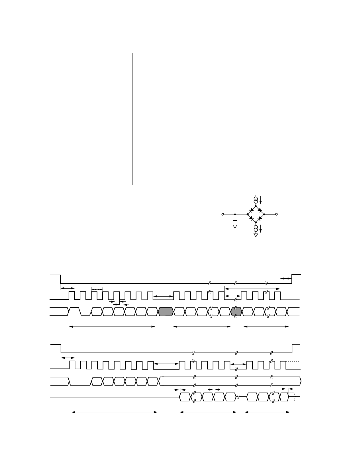
Figure 1. Load Circuit for Timing Specifications
50pF
I
200A
C
L
1.6mA
OL
2.1V
I
OH
CS
SCLK
DIN
CS
SCLK
DIN
DOUT
t
8
t
1
1
t
2
0
t
3
t
4
A5
A4
COMMAND BYTE
A3 A2
t
7
t
5
A1
A0
DB7
MOST SIGNIFICANT BYTE
t
7
DB0 DB7
t
6
DB0
LEAST SIGNIFICANT BYTE
Figure 2. Serial Write Timing
t
1
A4
A5
0
0
COMMAND BYTE
A2
A3
A1
t
9
A0
t
11
DB7
MOST SIGNIFICANT BYTE
t
10
t
t
12
DB0
DB7
LEAST SIGNIFICANT BYTE
13
DB0
Figure 3. Serial Read Timing
REV. 0–4–
ADE7754
ABSOLUTE MAXIMUM RATINGS*
(TA = +25°C, unless otherwise noted.)
AVDD to AGND . . . . . . . . . . . . . . . . . . . . . . . –0.3 V to +7 V
to DGND . . . . . . . . . . . . . . . . . . . . . . . –0.3 V to +7 V
DV
DD
to AVDD . . . . . . . . . . . . . . . . . . . . . . . –0.3 V to +0.3 V
DV
DD
Analog Input Voltage to AGND
, IAN, IBP, IBN, ICP, ICN, VAP, VBP, VCP, VN . . –6 V to +6 V
I
AP
Reference Input Voltage to AGND . –0.3 V to AV
Digital Input Voltage to DGND . . . –0.3 V to DV
+ 0.3 V
DD
+ 0.3 V
DD
Digital Output Voltage to DGND . . –0.3 V to DVDD + 0.3 V
Operating Temperature Range
Industrial . . . . . . . . . . . . . . . . . . . . . . . . . . –40°C to +85°C
Storage Temperature Range . . . . . . . . . . . . –65°C to +150°C
Junction Temperature . . . . . . . . . . . . . . . . . . . . . . . . . . 150°C
24-Lead SOIC, Power Dissipation . . . . . . . . . . . . . . . 88 mW
Thermal Impedance . . . . . . . . . . . . . . . . . . . . . . . . 53°C/W
JA
Lead Temperature, Soldering
Vapor Phase (60 sec) . . . . . . . . . . . . . . . . . . . . . . . . . 215°C
Infrared (15 sec) . . . . . . . . . . . . . . . . . . . . . . . . . . . . 220°C
*Stresses above those listed under Absolute Maximum Ratings may cause perma-
nent damage to the device. This is a stress rating only; functional operation of the
device at these or any other conditions above those listed in the operational
sections of this specification is not implied. Exposure to absolute maximum rating
conditions for extended periods may affect device reliability.
ORDERING GUIDE
Model Package Description Package Option*
ADE7754AR 24-Lead SOIC RW-24
ADE7754ARRL 24-Lead SOIC RW-24 in Reel
EVAL-ADE7754EB ADE7754 Evaluation Board
*RW = Small Outline (Wide Body Package in Tubes)
CAUTION
ESD (electrostatic discharge) sensitive device. Electrostatic charges as high as 4000 V readily
accumulate on the human body and test equipment and can discharge without detection. Although the
ADE7754 features proprietary ESD protection circuitry, permanent damage may occur on devices
subjected to high energy electrostatic discharges. Therefore, proper ESD precautions are recommended
to avoid performance degradation or loss of functionality.
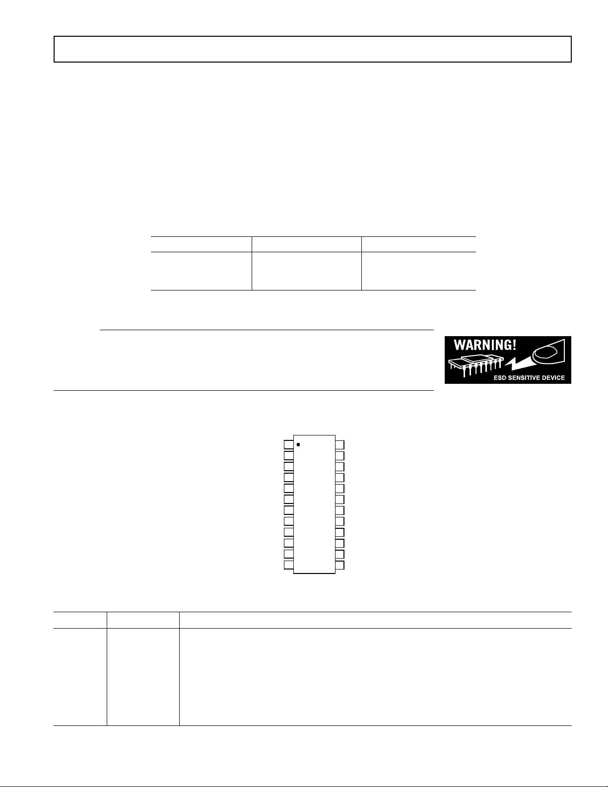
PIN CONFIGURATION
REF
CF
DGND
DV
AV
I
I
I
I
I
I
AGND
IN/OUT
DD
DD
AP
AN
BP
BN
CP
CN
1
2
3
4
5
ADE7754
6
TOP VIEW
(Not to Scale)
7
8
9
10
11
12
24
23
22
21
20
19
18
17
16
15
14
13
DOUT
SCLK
DIN
CS
CLKOUT
CLKIN
IRQ
RESET
V
AP
V
BP
V
CP
V
N
PIN FUNCTION DESCRIPTIONS
Pin No. Mnemonic Description
1CFCalibration Frequency Logic Output. This pin provides active power information. This output
is intended to be used for operational and calibration purposes. The full-scale output frequency
can be scaled by writing to the CFNUM and CFDEN registers. See the Energy to Frequency
Conversion section.
2 DGND This pin provides the ground reference for the digital circuitry in the ADE7754 (i.e. multiplier, filters,
and a digital-to-frequency converter). Because the digital return currents in the ADE7754 are small,
this pin can be connected to the analog ground plane of the whole system. However high bus
capacitance on the DOUT pin may result in noisy digital current, which could affect performance.
REV. 0
–5–

ADE7754
PIN FUNCTION DESCRIPTIONS (continued)
Pin No. Mnemonic Description
3DV
DD
Digital Power Supply. The supply voltage should be maintained at 5 V ± 5% for specified operation.
This pin should be decoupled to DGND with a 10 µF capacitor in parallel with a ceramic
100 nF capacitor.
4AV
DD
Analog Power Supply. The supply should be maintained at 5 V ± 5% for specified operation. Every
effort should be made to minimize power supply ripple and noise at this pin through the use of
proper decoupling. The TPCs chart the power supply rejection performance. This pin should be to
decoupled AGND with a 10 µF capacitor in parallel with a ceramic 100 nF capacitor.
5, 6; I
, IAN;Analog Inputs for Current Channel. This channel is intended for use with the current transducer
AP
7, 8; IBP, IBN; is referenced in this document as the current channel. These inputs are fully differential voltage
9, 10 I
CP
, I
CN
inputs with maximum differential input signal levels of ±0.5 V, ± 0.25 V, and ±0.125 V, depending
on the gain selections of the internal PGA. See the Analog Inputs section.
All inputs have internal ESD protection circuitry. An overvoltage of ±6 V can be sustained on these
inputs without risk of permanent damage.
11 AGND Analog Ground Reference. Used for ADCs, temperature sensor, and reference. This pin should be
tied to the analog ground plane or the quiet
ground reference should be used for all analog
and voltage transducers. To keep ground noise
est ground reference in the system. This quiet
circuitry such as anti-aliasing filters and current
around the ADE7754 to a minimum, the quiet
ground plane should be connected only to the digital ground plane at one point. It is acceptable to
place the entire device on the analog ground plane.
12 REF
IN/OUT
This pin provides access to the on-chip voltage reference, which has a nominal value of 2.4 V ± 8%
and a typical temperature coefficient of 30 ppm/°C. An external reference source may also be connected
at this pin. In either case, this pin should be decoupled to AGND with a 1 µF ceramic capacitor.
13, 14; V
15, 16 VBP, V
, VCP;
N
AP
Analog Inputs for the Voltage Channel. This channel is intended for use with the voltage transducer
and is referenced as the voltage channel in this document. These inputs are single-ended voltage
inputs with maximum signal level of ±0.5 V with respect to VN for specified operation. These
inputs are voltage inputs with maximum differential input signal levels of ±0.5 V, ±0.25 V, and
±0.125 V, depending on the gain selections of the internal PGA. See the Analog Inputs section.
All inputs have internal ESD protection circuitry. An overvoltage of ±6 V can be sustained on these
inputs without risk of permanent damage.
17 RESET Reset. A logic low on this pin holds the ADCs and digital circuitry (including the serial interface) in
a reset condition.
18 IRQ Interrupt Request Output. This is an active low, open-drain logic output. Maskable interrupts
include active energy register at half level, apparent energy register at half level, and waveform
sampling at up to 26 kSPS. See the Interrupts section.
19 CLKIN Master Clock for ADCs and Digital Signal Processing. An external clock can be provided at this logic
input. Alternatively, a parallel resonant AT crystal can be connected across CLKIN and CLKOUT
to provide a clock source for the ADE7754. The clock frequency for specified operation is 10 MHz.
Ceramic load capacitors of 22 pF to 33 pF should be used with the gate oscillator circuit. Refer to
the crystal manufacturer’s data sheet for load capacitance requirements.
20 CLKOUT A crystal can be connected across this pin and CLKIN as described above to provide a clock source
for the ADE7754. The CLKOUT pin can drive one CMOS load when an external clock is supplied
at CLKIN, or a crystal is used.
21 CS Chip Select. Part of the 4-wire serial interface. This active low logic input allows the ADE7754
to share the serial bus with several other devices. See the Serial Interface section.
22 DIN Data Input for the Serial Interface. Data is shifted in at this pin on the falling edge of SCLK. See
the Serial Interface section.
23 SCLK Serial Clock Input for the Synchronous Serial Interface. All serial data transfers are synchronized to
this clock. See the Serial Interface section. The SCLK has a Schmidt-trigger input for use with a
clock source that has a slow edge transition time (e.g., opto-isolator outputs).
24 DOUT Data Output for the Serial Interface. Data is shifted out at this pin on the rising edge of SCLK.
This logic output is normally in a high impedance state unless it is driving data onto the serial
data bus. See the Serial Interface section.
REV. 0–6–
Typical Performance Characteristics–ADE7754
0.50
WYE CONNECTION
GAIN = 1
0.40
PF = 1
INTERNAL REFERENCE
0.30
PHASE A
PHASE B
PHASE A + B + C
PHASE C
CURRENT (% fs)
0.20
0.10
0.00
–0.10
PERCENT ERROR
–0.20
–0.30
–0.40
–0.50
0.01 0.1 1 10 100
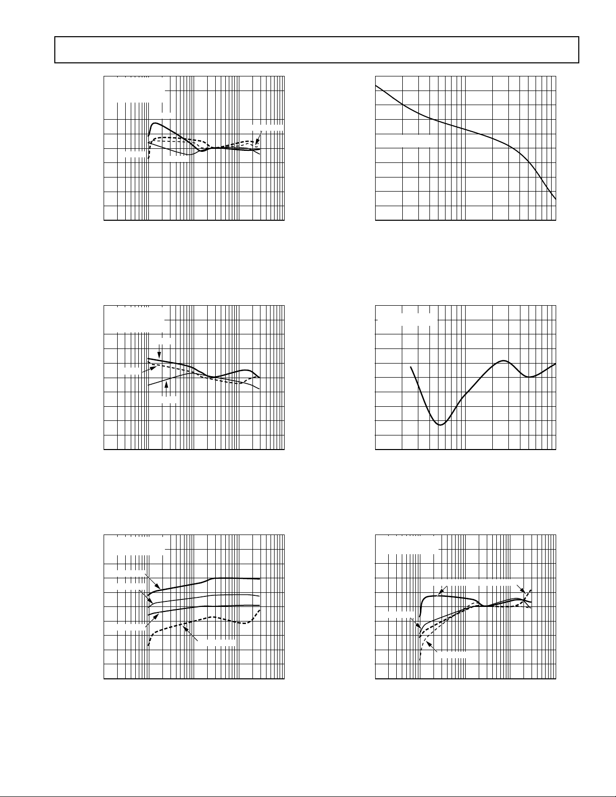
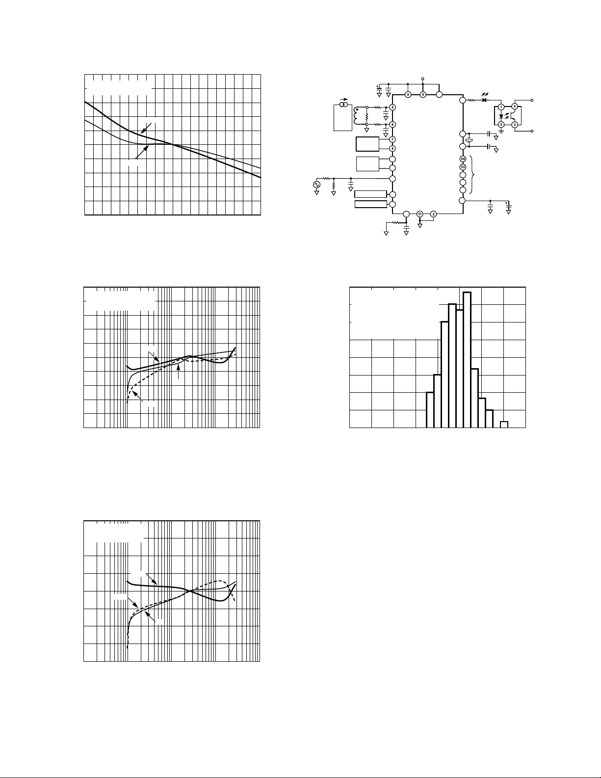
TPC 1. Real Power Error as a Percentage of
Reading with Gain = 1 and Internal Reference
(WYE Connection)
0.50
DELTA CONNECTION
GAIN = 1
0.40
PF = 0.5
INTERNAL REFERENCE
0.30
0.20
0.10
0.00
–0.10
PERCENT ERROR
–0.20
–0.30
–0.40
–0.50
0.01 0.1 1 10 100
PF = –0.5
PF = +1
PF = +0.5
CURRENT (% fs)
TPC 2. Real Power Error as a Percentage of
Reading over Power Factor with Internal
Reference (DELTA Connection)
1.00
0.80
0.60
0.40
0.20
GAIN = 1
INTERNAL REFERENCE
0.00
–0.20
PERCENT ERROR
–0.40
–0.60
–0.80
–1.00
110100
TPC 4.
Current RMS Error as a Percentage of
CURRENT INPUT (% fs)
Reading with Internal Reference (Gain = 1)
0.50
GAIN = 1
0.40
INTERNAL REFERENCE
0.30
0.20
0.10
0.00
–0.10
PERCENT ERROR
–0.20
–0.30
–0.40
–0.50
110100
VOLTAGE INPUT (% fs)
TPC 5. Voltage RMS Error as a Percentage of
Reading with Internal Reference (Gain = 1)
1.00
GAIN = 1
PF = 0.5
0.80
INTERNAL REFERENCE
0.60
+85∞C PF = +0.5
0.40
+25∞C PF = –0.5
0.20
0.00
–0.20
+25∞C PF = +1.0
PERCENT ERROR
–0.40
–0.60
–0.80
–1.00
0.01 0.1 1 10 100
TPC 3. Real Power Error as a
–40∞C PF = +0.5
CURRENT (% fs)
Percentage
over Power Factor with Internal Reference (Gain = 1)
REV. 0
of Reading
–7–
0.50
GAIN = 1
PF = 0.5
0.40
EXTERNAL REFERENCE
0.30
0.20
0.10
0.00
+25∞C PF = –0.5
–0.10
PERCENT ERROR
–0.20
–0.30
–0.40
–0.50
0.01 0.1 1 10 100
–40∞C PF = +0.5
VOLTAGE INPUT (% fs)
+85∞C PF = +0.5+25∞C PF = +1
TPC 6. Real Power Error as a Percentage of Reading
over Power Factor with External Reference (Gain = 1)
ADE7754
1.00
0.80
0.60
0.40
0.20
0.00
–0.20
PERCENT ERROR
–0.40
–0.60
–0.80
–1.00
45 50 55 60 65
GAIN = 1
INTERNAL REFERENCE
PF = 1
PF = 0.5
FREQUENCY (Hz)
220V
1M
1k
I
33nF
10F
33nF
RB
33nF
SAME AS
IAP, I
AN
SAME AS
IAP, I
AN
SAME AS V
SAME AS V
1k
1k
100nF
I
I
I
I
I
9
10
I
16
V
15
V
AP
V
14
AP
1k
33nF
V
DD
AVDD DVDD RESET
AP
ADE7754
AN
BP
BN
CP
CN
AP
BP
CP
VN AGND DGND
13
REF
17
CLKOUT
CLKIN
IN/OUT
DOUT
SCLK
CF
CS
DIN
IRQ
825
1
20
10MHz
19
21
22
18
12
PS2501-1
22pF
22pF
TO SPI BUS
ONLY USED FOR
CALIBRATION
100nF 10F
TO FREQ.
COUNTER
TPC 7. Real Power Error as a Percentage of Reading over Input Frequency with Internal Reference
0.20
GAIN = 1
PF = 1
0.16
EXTERNAL REFERENCE
0.12
0.08
0.04
4.75V
0.00
–0.04
PERCENT ERROR
–0.08
–0.12
5.25V
5V
–0.16
–0.20
0.01 0.1 1 10 100
CURRENT INPUT (% fs)
TPC 8. Real Power Error as a Percentage of Reading over Power Supply with External Reference
(Gain = 1)
0.20
GAIN = 1
PF = 1
INTERNAL REFERENCE
0.15
TPC 10. Test Circuit for Performance Curves
24
N = 116
MEAN = 4.33955
21
SD = 3.13475
LIMITS: LOW = –19, HIGH = +19
MIN = –2.21937
18
MAX = +14.7485
RANGE = 16.9669
15
12
9
PERCENT ERROR
6
3
0
–20
–15 –10 –5 0 5 10 15 20
CH_I PhA OFFSET (mV)
TPC 11. Current Channel Offset Distribution (Gain = 1)
0.10
0.05
0.00
–0.05
PERCENT ERROR
–0.10
4.75V
5.25V
5V
–0.15
–0.20
0.01 0.1 1
10 100
CURRENT INPUT (% fs)
TPC 9. Real Power Error as a Percentage of Reading
over Power Supply with Internal Reference (Gain = 1)
REV. 0–8–
ADE7754
TERMINOLOGY
Measurement Error
The error associated with the energy measurement made by the
ADE7754 is defined by the formula
Percentage Error
Energy gistered by ADE True Energy
=
Re 7754
True Energy
−
×
100%
Phase Error Between Channels
The HPF (high-pass filter) in the current channel has a phase
lead response. To offset this phase response and equalize the
phase response between channels, a phase correction network is
placed in the current channel. The phase correction network
ensures a phase match between the current channels and voltage
channels to within ±0.1° over a range of 45 Hz to 65 Hz and
±0.2° over a range of 40 Hz to 1 kHz. This phase mismatch
between the voltage and the current channels can be reduced
further with the phase calibration register in each phase.
Power Supply Rejection
This quantifies the ADE7754 measurement error as a percentage
of reading when power supplies are varied. For the ac PSR measurement, a reading at nominal supplies (5 V) is taken. A second
reading is obtained using the same input signal levels when an ac
(175 mV rms/100 Hz) signal is introduced onto the supplies. Any
error introduced by this ac signal is expressed as a percentage of
reading. See the Measurement Error definition above.
For the dc PSR measurement, a reading at nominal supplies
(5 V) is taken. A second reading is obtained using the same
input signal levels when the power supplies are varied ±5%. Any
error introduced is again expressed as a percentage of reading.
ADC Offset Error
This refers to the dc offset associated with the analog inputs to
the ADCs. It means that with the analog inputs connected to
AGND, the ADCs still see a dc analog input signal. The magnitude of the offset depends on the gain and input range selection
(see the TPCs). However, when HPFs are switched on, the
offset is removed from the current channels and the power
calculation is unaffected by this offset.
Gain Error
The gain error in the ADE7754 ADCs is defined as the difference between the measured ADC output code (minus the
offset) and the ideal output code. See the Current Channel
ADC and the Voltage Channel ADC sections. The difference is
expressed as a percentage of the ideal code.
Gain Error Match
Gain error match is defined as the gain error (minus the offset)
obtained when switching between a gain of 1, 2, or 4. It is
expressed as a percentage of the output ADC code obtained
under a gain of 1.
POWER SUPPLY MONITOR
The ADE7754 contains an on-chip power supply monitor. The
analog supply (AVDD) is continuously monitored by the ADE7754.
If the supply is less than 4 V ± 5%, the ADE7754 goes into an
inactive state (i.e., no energy is accumulated when the supply
voltage is below 4 V). This is useful to ensure correct device
operation at power-up and during power-down. The power supply monitor has built-in hysteresis and filtering, providing a high
degree of immunity to false triggering due to noisy supplies.
AV
DD
5V
4V
POWER-ON
RESET FLAG IN
THE INTERRUPT
STATUS REGISTER
READ RSTATUS
REGISTER
0V
INACTIVE
TIME
ACTIVE
INACTIVE
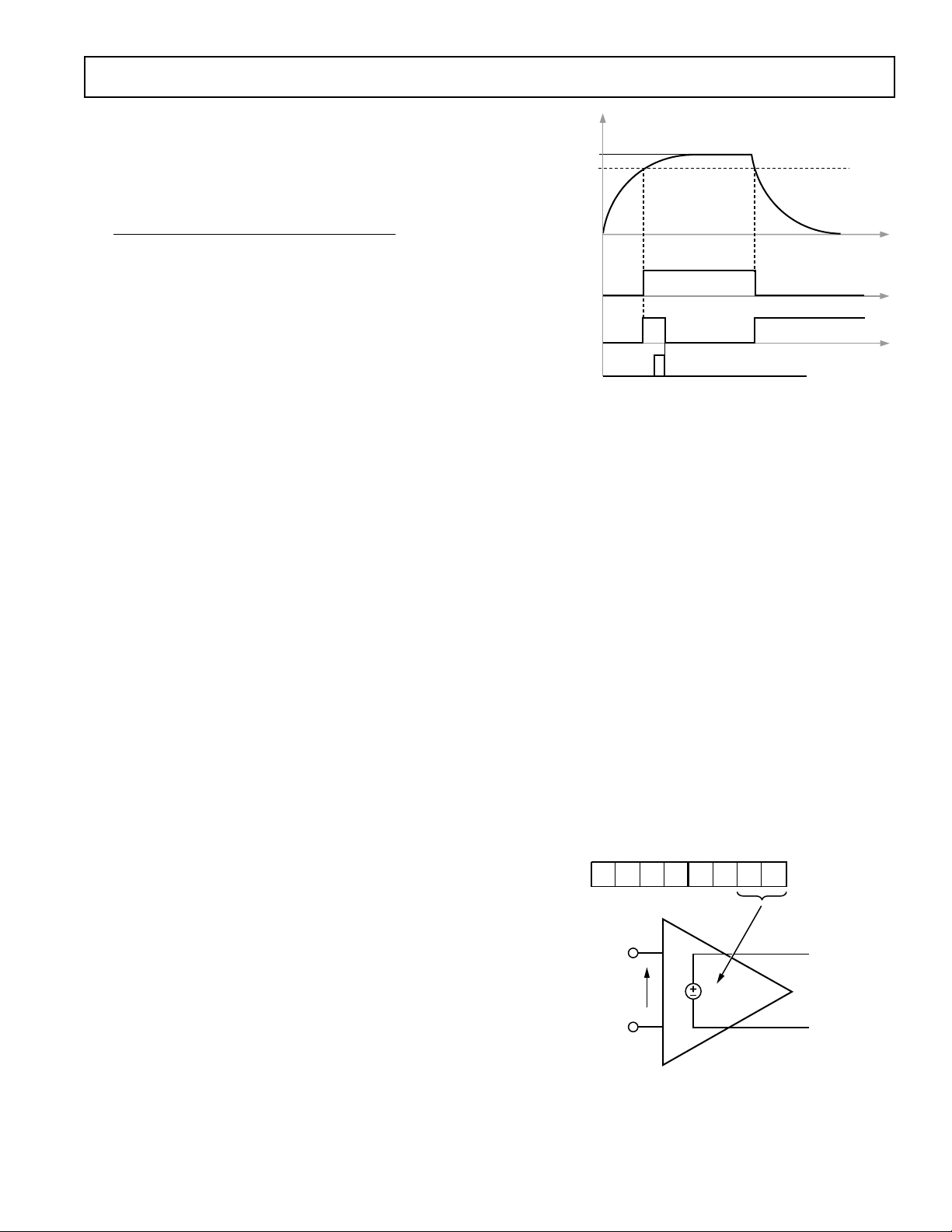
Figure 4. On-Chip Power Supply Monitoring
The RESET bit in the interrupt status register is set to Logic 1
when AV
drops below 4 V ± 5%. The RESET flag is always
DD
masked by the interrupt enable register and cannot cause the
IRQ pin to go low. The power supply and decoupling for the
part should ensure that the ripple at AV
does not exceed 5 V
DD
± 5% as specified for normal operation.
ANALOG INPUTS
The ADE7754 has six analog inputs, divisible into two channels: current and voltage. The current channel consists of three
pairs of fully differential voltage inputs: I
, ICN. The fully differential voltage input pairs have a maxi-
I
CP
, IAN; IBP, IBN; and
AP
mum differential voltage of ±0.5 V. The voltage channel has
three single-ended voltage inputs: V
, VBP, and VCP. These
AP
single-ended voltage inputs have a maximum input voltage of
±0.5 V with respect to V
. Both the current channel and the
N
voltage channel have a PGA (programmable gain amplifier) with
possible gain selections of 1, 2, or 4. The same gain is applied to
all the inputs of each channel.
The gain selections are made by writing to the gain register. Bits 0
and 1 select the gain for the PGA in the fully differential current
channel. The gain selection for the PGA in the single-ended voltage channel is made via Bits 5 and 6. Figure 5 shows how a gain
selection for the current channel is made using the gain register.
GAIN[7:0]
GAIN (k)
IAP, IBP, I
IAN, IBN, I
CP
V
IN
CN
k V
SELECTION
IN
Figure 5. PGA in Current Channel
REV. 0
–9–
ADE7754
Figure 6 shows how the gain settings in PGA 1 (current channel)
and PGA 2 (voltage channel) are selected by various bits in the
gain register. The no-load threshold and sum of the absolute
value can also be selected in the gain register. See Table X.
CURRENT AND VOLTAGE CHANNEL PGA CONTROL
7
0
RESERVED = 0
PGA 2 GAIN SELECT
00 = 1
01 = 2
10 = 4
*REGISTER CONTENTS SHOW POWER-ON DEFAULTS
GAIN REGISTER*
6
5
0
0
RESERVED = 0
4
0
2
3
0
0
ABS
NO LOAD
0
1
0
0
ADDR: 18h
PGA 1 GAIN SELECT
00 = 1
01 = 2
10 = 4
Figure 6. Analog Gain Register
ANALOG-TO-DIGITAL CONVERSION
The ADE7754 carries out analog-to-digital conversion using
second order Σ-∆ ADCs. The block diagram in Figure 7 shows a
first order (for simplicity) Σ-∆ ADC. The converter is made up of
two parts, the Σ-∆ modulator and the digital low-pass filter.
MCLK/12
ANALOG
LOW-PASS FILTER
R
C
+
INTEGRATOR
–
V
REF
1-BIT DAC
LATCHED
COMPARATOR
....10100101......
1
DIGITAL
LOW-PASS
FILTER
24
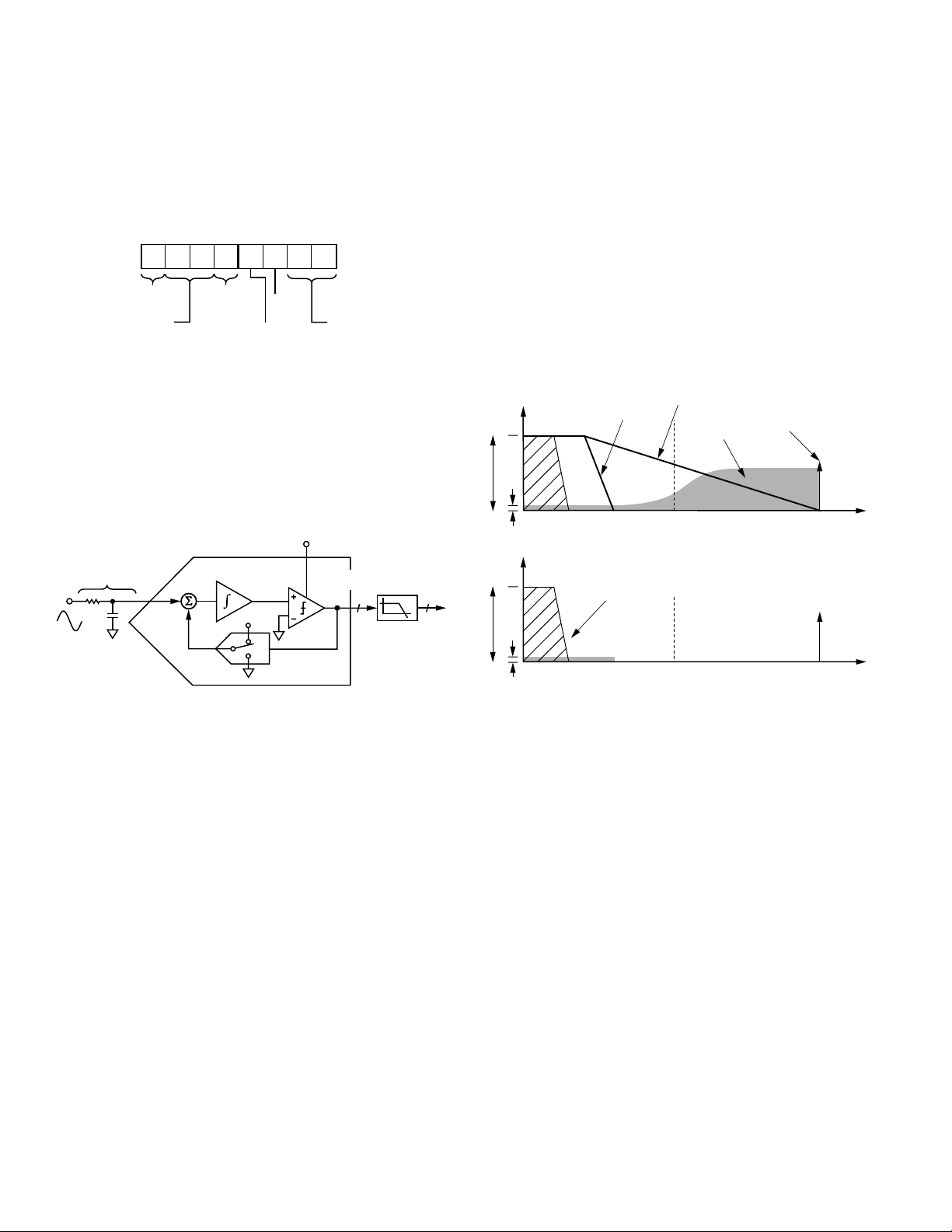
Figure 7. First Order (-) ADC
A Σ-∆ modulator converts the input signal into a continuous
serial stream of 1s and 0s at a rate determined by the sampling
clock. In the ADE7754, the sampling clock is equal to CLKIN/12.
The 1-bit DAC in the feedback loop is driven by the serial data
stream. The DAC output is subtracted from the input signal.
If the loop gain is high enough, the average value of the DAC
output (and therefore the bit stream) will approach that of the
input signal level. For any given input value in a single sam
interval, the data from the 1-bit ADC is virtually meaningless.
pling
Only
when a large number of samples are averaged will a meaningful
result be obtained. This averaging is carried out in the second part
of the ADC, the digital low-pass filter. Averaging a large number of
bits from the modulator, the low-pass filter can produce 24-bit
data-words that are proportional to the input signal level.
The Σ-∆ converter uses two techniques to achieve high resolution from what is essentially a 1-bit conversion technique. The
first is oversampling; the signal is sampled at a rate (frequency)
many times higher than the bandwidth of interest. For
the sampling rate in the ADE7754 is CLKIN/12
example,
(833 kHz),
and the band of interest is 40 Hz to 2 kHz. Oversampling
spreads the quantization noise (noise due to sampling) over a
wider bandwidth. With the noise spread more thinly over a
wider bandwidth, the quantization noise in the band of interest
is lowered. See Figure 8.
Oversampling alone is not an efficient enough method to
improve
the signal to noise ratio (SNR) in the band of interest.
For example, an oversampling ratio of 4 is required to increase
the SNR by only 6 dB (1 bit). To keep the oversampling ratio at
a reasonable level, the quantization noise can be shaped so that
most of the noise lies at the higher frequencies. In the Σ-∆
modulator, the noise is shaped by the integrator, which has a
high-pass type of response for the quantization noise. The result
is that most of the noise is at the higher frequencies, where it
can be removed by the digital low-pass filter. This noise shaping
is shown in Figure 8.
ANTIALIAS FILTER (RC)
SIGNAL
NOISE
SIGNAL
NOISE
DIGITAL FILTER
0
2
FREQUENCY (kHz)
HIGH RESOLUTION
OUTPUT FROM DIGITAL
LPF
0
2
FREQUENCY (kHz)
417
417
SHAPED
NOISE
SAMPLING
FREQUENCY
833
833
Figure 8. Noise Reduction Due to Oversampling
and Noise Shaping in the Analog Modulator
Antialias Filter
Figure 7 shows an analog low-pass filter (RC) on the input to
the modulator. This filter is used to prevent aliasing, an artifact
of all sampled systems. Frequency components in the input
signal to the ADC that are higher than half the sampling rate of
the ADC appear in the sampled signal at a frequency below half
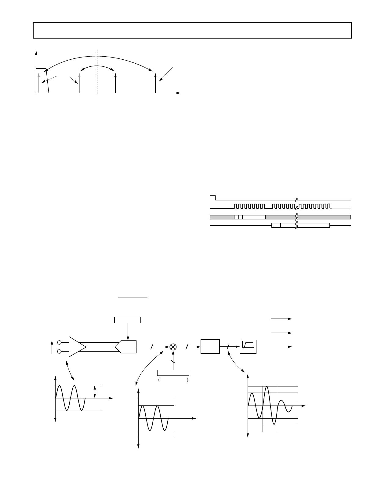
the sampling rate. Figure 9 illustrates the effect; frequency components (arrows shown in black) above half the sampling
frequency (also known as the Nyquist frequency), i.e., 417 kHz,
get imaged or folded back down below 417 kHz (arrows shown
in gray). This happens with all ADCs, regardless of the architecture. In the example shown, only frequencies near the sampling
frequency, i.e., 833 kHz, will move into the band of interest for
metering, i.e., 40 Hz to 2 kHz. This allows use of a very simple
LPF (low-pass filter) to attenuate these high frequencies (near
900 kHz) and thus prevent distortion in the band of interest. A
simple RC filter (single pole) with a corner frequency of 10 kHz
produces an attenuation of approximately 40 dBs at 833 kHz.
See Figure 9. This is sufficient to eliminate the effects of aliasing.
REV. 0–10–
ADE7754
ALIASING EFFECTS
SAMPLING
FREQUENCY
833
0
IMAGE
FREQUENCIES
2
417
FREQUENCY (kHz)
Figure 9. ADC and Signal Processing in Current
Channel or Voltage Channel
CURRENT CHANNEL ADC
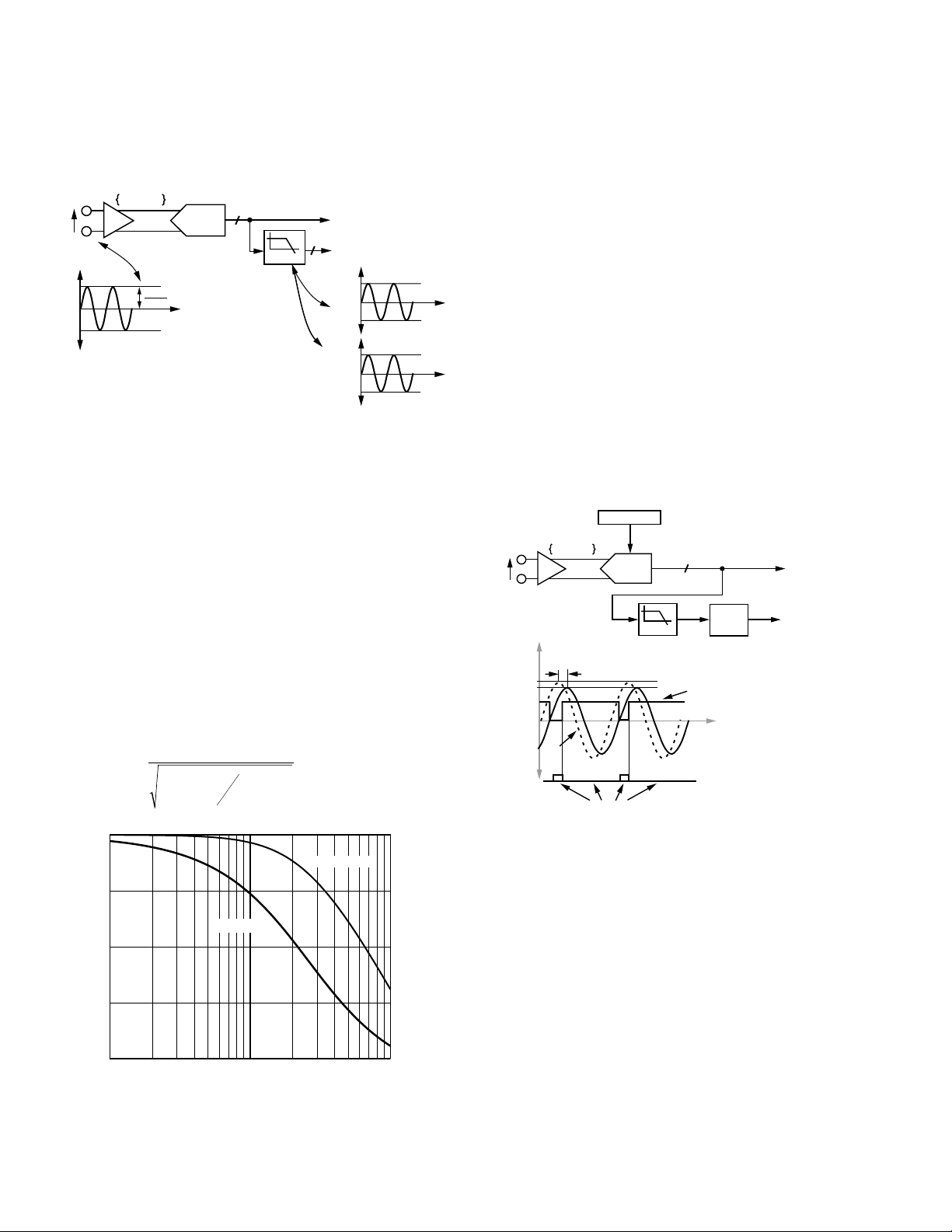
Figure 10 shows the ADC and signal processing chain for the
input IA of the current channels (which are the same for IB and
IC). In waveform sampling mode, the ADC outputs are signed
twos complement 24-bit data-word at a maximum of 26 kSPS
(kilo samples per second). The output of the ADC can be
scaled by ±50% by using the APGAINs register. While the
ADC outputs are 24-bit twos complement value, the maximum
full-scale positive value from the ADC is limited to 400000h
(+4,194,304d). The maximum full-scale negative value is limited to C00000h (–4,194,304d). If the analog inputs are
overranged, the ADC output code clamps at these values. With
the specified full-scale analog input signal of ±0.5 V, the ADC
produces an output code between D70A3Eh (–2,684,354) and
28F5C2h (+2,684,354), as illustrated in Figure 10, which also
shows a full-scale voltage signal being applied to the differential
inputs I
and IAN.
AP
Current Channel ADC Gain Adjust
The ADC gain in each phase of the current channel can be
adjusted using the multiplier and active power gain register
(AAPGAIN[11:0], BAPGAIN, and CAPGAIN). The gain of the
ADC is adjusted by writing a twos complement 12-bit word to
the active power gain register. The following expression shows
how the gain adjustment is related to the contents of that register:
For example, when 7FFh is written to the active power gain
register, the ADC output is scaled up by 50%: 7FFh = 2047d,
2047/212 = 0.5. Similarly, 800h = –2047d (signed twos complement) and ADC output is scaled by –50%. These two examples
are illustrated in Figure 10.
Current Channel Sampling
The waveform samples of the current channel inputs may also
be routed to the waveform register (wavmode register to select
the speed and the phase) to be read by the system master
(MCU). The active energy and apparent energy calculation remains
uninterrupted during waveform sampling.
When in waveform sample mode, one of four output sample
rates may be chosen using Bits 3 and 4 of the WAVMODE
register (DTRT[1:0] mnemonic). The output sample rate
may be 26.0 kSPS, 13.0 kSPS, 6.5 kSPS, or 3.3 kSPS. See the
Waveform Mode Register section. By setting the WSMP bit in
the interrupt enable register to Logic 1, the interrupt request
IRQ
output
will go active low when a sample is available. The
timing is shown in Figure 11. The 24-bit waveform samples are
transferred from the ADE7754 one byte (eight bits) at a time,
with the most significant byte shifted out first.
IRQ
SCLK
DIN
DOUT
READ FROM WAVEFORM
0
0
09h
CURRENT CHANNEL DATA – 24 BITS
SGN
Figure 11. Waveform Sampling Current Channel
The interrupt request output IRQ stays low until the interrupt
routine reads the reset status register. See the Interrupt section.
Note that if the WSMP bit in the interrupt enable register is not
set to Logic 1, no data is available in the waveform register.
V
IN
REV. 0
0V
V
IN
I
AP
I
AN
ANALOG
INPUT
RANGE
Code ADC
=×+
ⴛ1, ⴛ2, ⴛ4
GAIN[1:0]
PGA1
100% FS
0.5V/GAIN1
1
AAPGAIN
12
2
REFERENCE
ADC
400000h
28F5C2h
000000h
D70A3Eh
C00000h
MULTIPLIER
1
800h–7FFh
AAPGAIN[11:0]
ADC OUTPUT
WORD RANGE
12
1
+100% FS
–100% FS
DIGITAL LPF
3
SINC
24
3D70A3h
28F5C2h
147AE1h
00000h
EB851Fh
D70A3Eh
C28F5Dh
Figure 10. ADC and Signal Processing in Current Channel
–11–
HPF
CHANNEL 1
000h
7FFh
CURRENT RMS
CALCULATION
WAVEFORM SAMPLE
REGISTER
ACTIVE AND REACTIVE
POWER CALCULATION
+ 150% FS
+ 100% FS
+ 50% FS
– 50% FS
– 100% FS
800h
– 150% FS
AAPGAIN[11:0]
ADE7754
VOLTAGE CHANNEL ADC
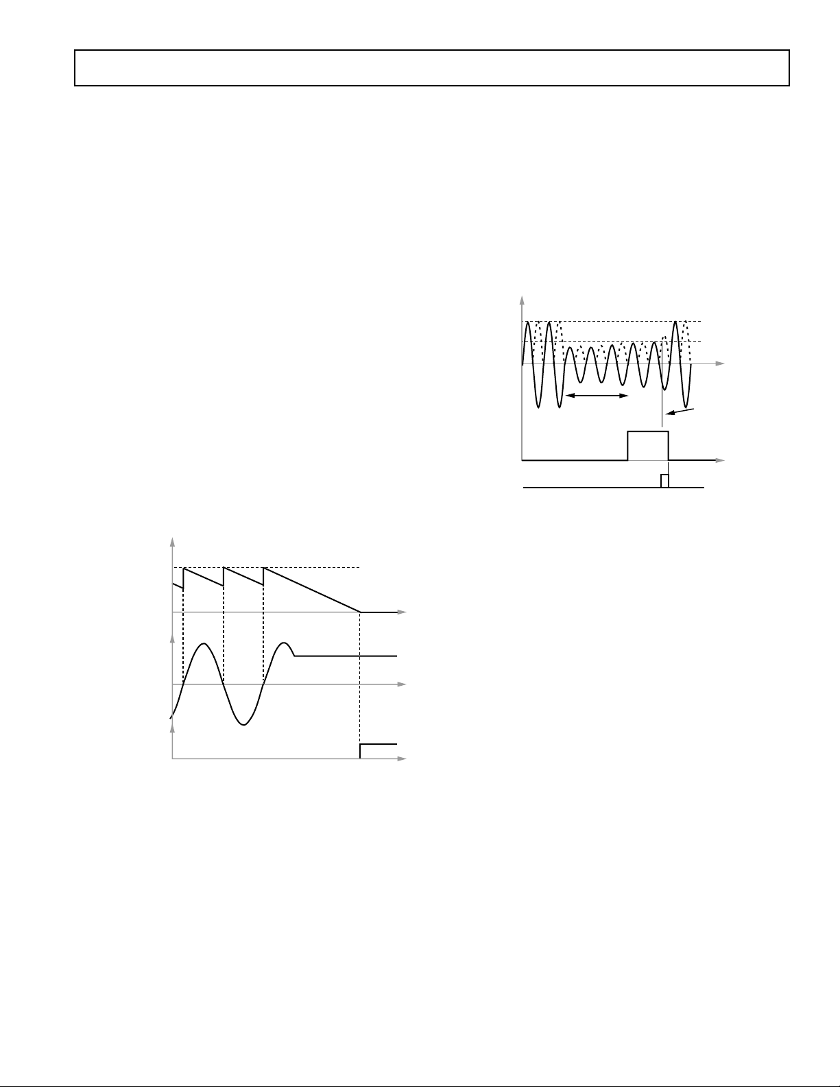
Figure 12 shows the ADC and signal processing chain for the
input VA in voltage channel (which is the same for VB and VC).
1, 2, 4
V
GAIN[6:5]
AP
VA
V
VA
0V
ANALOG
INPUT RANGE
ADC
N
0.5V
GAIN
60Hz
1
–100% TO +100% FS
LPF1
LPF OUTPUT
WORD RANGE
TO ACTIVE AND
REACTIVE ENERGY
CALCULATION
16
TO VOLTAGE RMS AND
WAVEFORM SAMPLING
27E9h
D817h
2838h
D7C8h
60Hz
50Hz
Figure 12. ADC and Signal Processing in Voltage Channel
For energy measurements, the output of the ADC (one bit) is
passed directly to the multiplier and is not filtered. This solution
avoids a wide-bits multiplier and does not affect the accuracy of
the measurement. An HPF is not required to remove any dc
offset since it is only required to remove the offset from one
channel to eliminate errors in the power calculation.
In the voltage channel, the samples may also be routed to the
WFORM register (WAVMODE to select VA, VB, or VC and
sampling frequency). However, before being passed to the waveform register, the ADC output is passed through a single-pole,
low-pass filter with a cutoff frequency of 260 Hz. The plots in
Figure 13 show the magnitude and phase response of this filter.
The filter output code of any inputs of the voltage channel
swings between D70Bh (–10,485d) and 28F5h (+10,485d) for
full-scale sine wave inputs. This has the effect of attenuating the
signal. For example, if the line frequency is 60 Hz, the signal at
the output of LPF1 will be attenuated by 3%.
|()| . –.Hf
0
–20
–40
PHASE (Degrees)
–60
–80
1
10
1
60
Hz
+
1
260
Hz
(60Hz; –13)
2
10
FREQUENCY (Hz)
0 974 0 2
==
2
(60Hz; –0.2dB)
dBs=
0
–10
–20
GAIN (dB)
–30
–40
3
10
Figure 13. Magnitude and Phase Response of LPF1
Note that LPF1 does not affect the power calculation because it
is used only in the waveform sample mode and rms calculation.
In waveform sample mode, one of four output sample rates
can be chosen by using Bits 3 and 4 of the WAVMODE register. The available output sample rates are 26 kSPS, 13.5 kSPS,
6.5 kSPS, or 3.3 kSPS. The interrupt request output IRQ
signals a new sample availability by going active low. The
voltage waveform register is a twos complement 16-bit register.
Because the waveform register is a 24-bit signed register, the
waveform data from the voltage input is located in the 16 LSB of
the waveform register. The sign of the 16-bit voltage input value
is not extended to the upper byte of the waveform register. The
upper byte is instead filled with zeros. 24-bit waveform samples
are transferred from the ADE7754 one byte (eight bits) at a time,
with the most significant byte shifted out first. The timing is the
same as that for the current channels and is shown in Figure 11.
ZERO-CROSSING DETECTION
The ADE7754 has rising edge zero-crossing detection circuits
for each of voltage channels (V
, VBP, and VCP). Figure 14
AP
shows how the zero-cross signal is generated from the output of
the ADC of the voltage channel.
REFERENCE
VAP, VBP, VCP,
V
V
N
1.0
0.95
1, 2, 4
GAIN[6:5]
13 DEGREES AT 60Hz
V
READ RSTATUS
ADC
f
–3dB
1
LPF1
= 260Hz
IRQ
TO
MULTIPLIER
–100% TO +100% FS
ZERO
CROSS
ZERO-CROSSING
DETECTION
Figure 14. Zero-Crossing Detection on Voltage Channel
The zero-crossing interrupt is generated from the output of
LPF1, which has a single pole at 260 Hz (CLKIN = 10 MHz).
As a result, there is a phase lag between the analog input signal
of the voltage channel and the output of LPF1. The phase
response of this filter is shown in the Voltage Channel ADC
section. The phase lag response of LPF1 results in a time delay
of approximately 0.6 ms (@ 60 Hz) between the zero crossing
on the analog inputs of voltage channel and the falling of IRQ.
When one phase crosses zero from negative to positive values
(rising edge), the corresponding flag in the interrupt status
register (Bits 7 to 9) is set Logic 1. An active low in the IRQ
output also appears if the corresponding ZX bit in the interrupt
enable register is set to Logic 1.
The flag in the interrupt status register is reset to 0 when the interrupt status register with reset (RSTATUS) is read. Each phase has
its own interrupt flag and enable bit in the interrupt register.
REV. 0–12–
ADE7754
In addition to the enable bits, the zero-crossing detection interrupt
of each phase is enabled/disabled by setting the ZXSEL bits of the
MMODE register (Address 0Bh) to Logic 1 or 0, respectively.
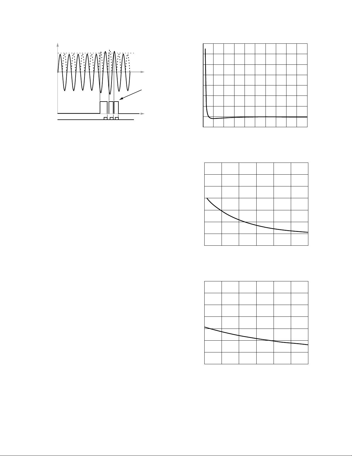
Zero-Crossing Timeout
Each zero-crossing detection has an associated internal timeout
register (not accessible to the user). This unsigned, 16-bit register is decremented (1 LSB) every 384/CLKIN seconds. The
registers are reset to a common user programmed value (i.e.,
zero cross timeout register—ZXTOUT, Address 12h) every
time a zero crossing is detected on its associated input. The
default value of ZXTOUT is FFFFh. If the internal register
decrements to zero before a zero crossing at the corresponding
input is detected, it indicates an absence of a zero crossing in
the time determined by the ZXTOUT. The ZXTO detection
bit of the corresponding phase in the interrupt status register is
then switched on (Bits 4 to 6). An active low on the IRQ output
also appears if the SAG enable bit for the corresponding phase
in the interrupt enable register is set to Logic 1.
In addition to the enable bits, the zero-crossing timeout detection interrupt of each phase is enabled/disabled by setting the
ZXSEL bits of the MMODE register (Address 0Bh) to Logic 1
or Logic 0, respectively. When the zero-crossing timeout detection
is disabled by this method, the ZXTO flag of the corresponding
phase is switched on all the time.
Figure 15 shows the mechanism of the zero-crossing timeout
detection when the line voltage A stays at a fixed dc level for
more than CLKIN/384 ZXTOUT seconds.
16-BIT INTERNAL
REGISTER VALUE
ZXTOUT
VOLTAGE
CHANNEL A
ZXTOA
DETECTION BIT
Figure 15. Zero-Crossing Timeout Detection
PERIOD MEASUREMENT
The ADE7754 also provides the period measurement of the
line voltage. The period is measured on the phase specified by
Bits 0 to 1 of the MMODE register. The period register is an
unsigned 15-bit register and is updated every period of the
selected phase. Bits 0 and 1 and Bits 4 to 6 of the MMODE
register select the phase for the period measurement; both
selections should indicate the same phase. The ZXSEL bits of
the MMODE register (Bits 4 to 6) enable the phases on which
the period measurement can be done. The PERDSEL bits
select the phase for period measurement within the phases
selected by the ZXSEL bits.
The resolution of this register is 2.4 µs/LSB when CLKIN =
10 MHz
, which is 0.014% when the line frequency is 60 Hz.
When the line frequency is 60 Hz, the value of the period register is approximately 6944d. The length of the register enables
the measurement of line frequencies as low as 12.7 Hz.
LINE VOLTAGE SAG DETECTION
The ADE7754 can be programmed to detect when the absolute
value of the line voltage of any phase drops below a certain peak
value for a number of half cycles. All phases of the voltage channel are controlled simultaneously. This condition is illustrated
in Figure 16.
FULL SCALE
SAGLVL[7:0]
SAG INTERRUPT
(BIT 1 TO
FLAG
BIT 3 OF STATUS
REGISTER)
READ
RSTATUS
REGISTER
VAP, VBP, OR V
SAGCYC[7:0] = 06h
6 HALF CYCLES
CP
SAG EVENT RESET
LOW WHEN VOLTAGE
CHANNEL EXCEEDS
SAGLVL[7:0]
Figure 16. SAG Detection
Figure 16 shows a line voltage falling below a threshold set in
the SAG level register (SAGLVL[7:0]) for nine half cycles.
the SAG cycle register indicates a six half-cycle thresh-
Since
old (SAGCYC[7:0]=06h),
the SAG event is recorded at the
end of the sixth half-cycle by setting the SAG flag of the corresponding phase in the interrupt status register (Bits 1 to 3 in the
interrupt status register). If the SAG enable bit is set to Logic 1
for this phase (Bits 1 to 3 in the interrupt enable register), the
IRQ logic output goes active low. See the Interrupts section. All
the phases are compared to the same parameters defined in the
SAGLVL and SAGCYC registers.
SAG Level Set
The content of the SAG level register (one byte) is compared to
the absolute value of the most significant byte output from the
voltage channel ADC. Thus, for example, the nominal maximum
code from the voltage channel ADC with a full-scale signal is
28F5h. See the Voltage Channel ADC section.
Therefore, writing 28h to the SAG level register puts the SAG
detection level at full scale and sets the SAG detection to its
most sensitive value.
Writing 00h puts the SAG detection level at 0. The detection of
a decrease of an input voltage is in this case hardly possible.
The detection is made when the content of the SAGLVL
register is greater than the incoming sample.
PEAK DETECTION
The ADE7754 also can be programmed to detect when the
absolute value of the voltage or the current channel of one phase
exceeds a certain peak value. Figure 17 illustrates the behavior
of the peak detection for the voltage channel.
REV. 0
–13–
ADE7754
k
VPEAK[7:0]
PKV INTERRUPT
FLAG (BIT C OF
STATUS REGISTER)
READ
RSTATUS
REGISTER
VAP, VBP, OR V
CP
PKV RESET
LOW WHEN
RSTATUS
REGISTER
IS READ
Figure 17. Peak Detection
Bits 2 and 3 of the measurement mode register define the phase
supporting the peak detection. Current and voltage of this phase
can be monitored at the same time. Figure 17 shows a line
voltage exceeding a threshold set in the voltage peak register
(VPEAK[7:0]). The voltage peak event is recorded by setting
the PKV flag in the interrupt status register. If the PKV enable
bit is set to Logic 1 in the interrupt enable register, the IRQ
logic output goes active low. See the Interrupts section.
Peak Level Set
The contents of the VPEAK and IPEAK registers compare to
the absolute value of the most significant byte output of the
selected voltage and current channels, respectively. Thus, for
example, the nominal maximum code from the current channel
ADC with a full-scale signal is 28F5C2h. See the Current
Channel Sampling section. Therefore, writing 28h to the
IPEAK register will put the current channel peak detection level
at full scale and set the current peak detection to its least sensitive value. Writing 00h puts the current channel detection level at
zero. The detection is done when the content of the IPEAK
register is smaller than the incoming current channel sample.
TEMPERATURE MEASUREMENT
The ADE7754 also includes an on-chip temperature sensor. A
temperature measurement is made every 4/CLKIN seconds.
The output from the temperature sensing circuit is connected
to an ADC for digitizing. The resulting code is processed and
placed into the temperature register (TEMP[7:0]) which can
be read by the user and has an address of 08h. See the Serial
Interface section. The contents of the temperature register are
signed (twos complement) with a resolution of 4°C/LSB. The
temperature register produces a code of 00h when the ambient
temperature is approximately 129°C. The value of the register is
temperature register = (temperature (°C) – 129)/4. The temperature in the ADE7754 has an offset tolerance of approximately
±5°C. The error can be easily calibrated out by an MCU.
PHASE COMPENSATION
When the HPFs are disabled, the phase difference between the
current channel (IA, IB, and IC) and the voltage channel (VA,
VB, and VC) is zero from dc to 3.3 kHz. When the HPFs are
enabled, the current channels have a phase response as shown in
Figure 18a and 18b. The magnitude response of the filter is
shown in Figure 18c. As seen from in the plots, the phase response
is almost zero from 45 Hz to 1 kHz. This is all that is required
in typical energy measurement applications.
0.07
0.06
0.05
0.04
0.03
0.02
PHASE (Degrees)
0.01
0
–0.01
0 200 400 600 800
100 300 500 700
FREQUENCY (Hz)
900
1
Figure 18a. Phase Response of the HPF and
Phase Compensation (10 Hz to 1 kHz)
0.010
0.008
0.006
0.004
0.002
PHASE (Degrees)
0
–0.002
–0.004
40 45 50 55 60
FREQUENCY (Hz)
65 70
Figure 18b. Phase Response of the HPF and
Phase Compensation (40 Hz to 70 Hz)
0.010
0.008
0.006
0.004
0.002
PHASE (Degrees)
0
–0.002
–0.004
44 46 48 50 52
FREQUENCY (Hz)
54 56
Figure 18c. Gain Response of HPF and Phase Compensation (Deviation of Gain as % of Gain at 54 Hz)
Despite being internally phase compensated, the ADE7754 must
work with transducers that may have inherent phase errors. For
example, a phase error of 0.1° to 0.3° is not uncommon for a CT
(current transformer). These phase errors can vary from part to
part, and they must be corrected in order to perform accurate
power calculations. The errors associated with phase mismatch
REV. 0–14–
 Loading...