PRELIMINARY TECHNICAL DATA
Three Phase Energy Metering IC
=
Preliminary Technical Data
FEATURES
High Accuracy, Supports 50 Hz/60 Hz IEC 687/1036
Less than 0.1% Error Over a Dynamic Range of
500 to 1
Compatible with 3-phase/3-wire and 3-phase/4-wire
configurations
The ADE7752 Supplies Average Real Power on the
Frequency Outputs F1 and F2
The High Frequency Output CF Is Intended for
Calibration and Supplies
The Logic Output REVP indicates a Potential Miswiring or
Negative Power for each phase
Direct Drive for Electromechanical Counters and
Two Phase Stepper Motors (F1 and F2)
Proprietary ADCs and DSP Provide High Accuracy over
Large Variations in Environmental Conditions and
Time
On-Chip Power Supply Monitoring
On-Chip Creep Protection (No Load Threshold)
On-Chip Reference 2.5 V ± 8% (30 ppm/8C Typical)
with External Overdrive Capability
Single 5 V Supply, Low Power (15 mW Typical)
Low Cost CMOS Process
Instantaneous Real Power
with Pulse Output
ADE7752*
GENERAL DESCRIPTION
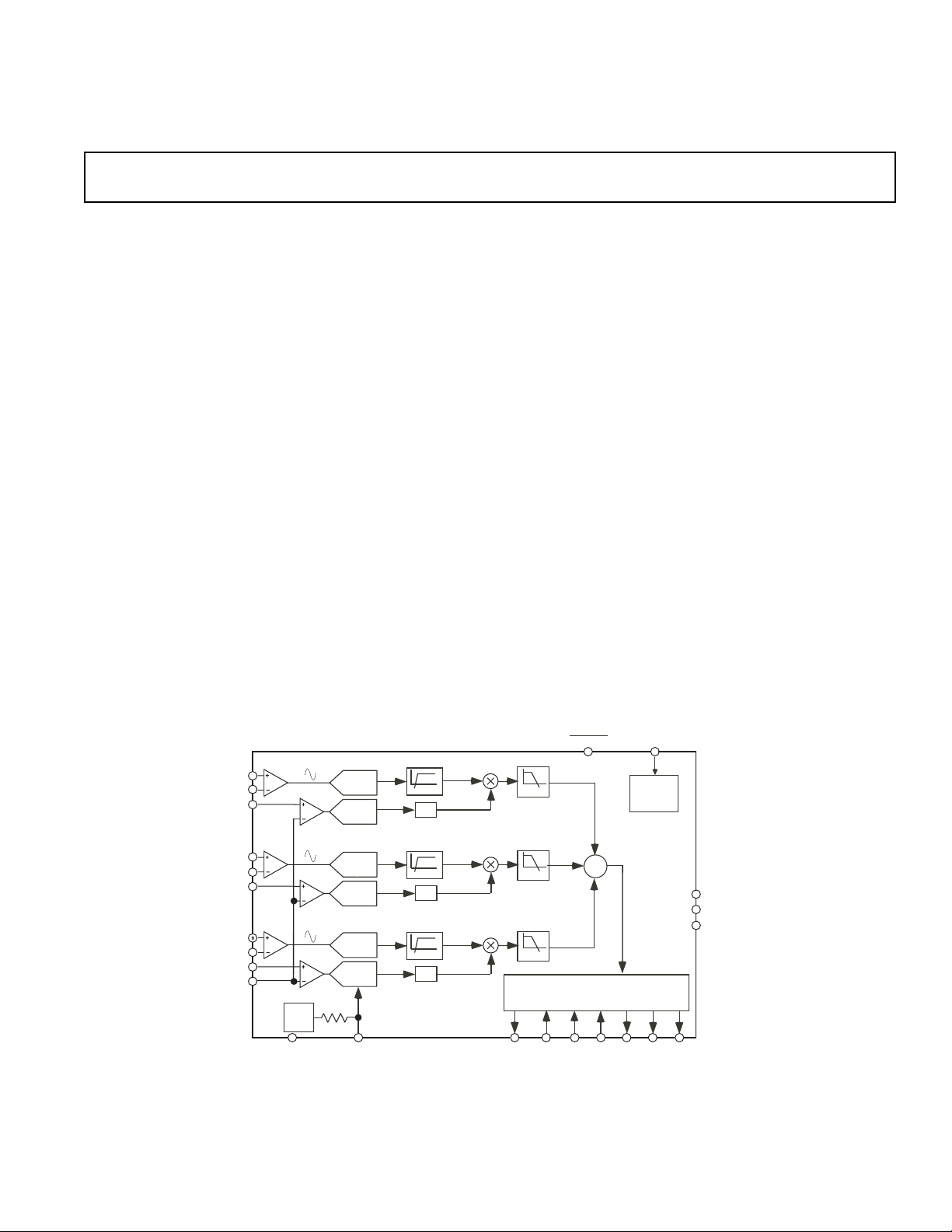
The ADE7752 is a high accuracy three phase electrical
energy measurement IC. The part specifications surpass the
accuracy requirements as quoted in the IEC1036 standard.
The only analog circuitry used in the ADE7752 is in the
ADCs and reference circuit. All other signal processing (e.g.,
multiplication, filtering and summation) is carried out in the
digital domain. This approach provides superior stability and
accuracy over extremes in environmental conditions and over
time.
The ADE7752 supplies average real power information on
the low frequency outputs F1 and F2. These logic outputs
may be used to directly drive an electromechanical counter or
interface with an MCU. The CF logic output gives instantaneous real power information. This output is intended to be
used for calibration purposes, or as interface with an MCU.
The ADE7752 includes a power supply monitoring circuit
on the AV
until the supply voltage on V
below 4 V, the ADE7752 will also be reset and no pulses will
be issued on F1, F2 and CF.
Internal phase matching circuitry ensures that the voltage and
current channels are phase matched. An internal no-load
threshold ensures that the ADE7752 does not exhibit any
creep when there is no load.
The ADE7752 is available in 24-lead SOIC packages.
supply pin. The ADE7752 will remain inactive
DD
reaches 4 V. If the supply falls
DD
FUNCTIONAL BLOCK DIAGRAM
5
*Patents pending
IAP
IAN
VAP
IBP
IBN
VBP
ICP
ICN
VCP
VN
6
16
7
8
15
10
14
13
2.5V
REF
11 12 4 18 21 22 23 24 1
AGND
4kΩ
ADC
ADC
ADC
ADC
ADC
ADC
REF
CORRECTION
CORRECTION
CORRECTION
IN/OUT
HPF
Φ
PHASE
HPF
Φ
PHASE
HPF
Φ
PHASE
REV. PrB 08/01
Information furnished by Analog Devices is believed to be accurate and
reliable. However, no responsibility is assumed by Analog Devices for its
use, nor for any infringements of patents or other rights of third parties
which may result from its use. No license is granted by implication or
otherwise under any patent or patent rights of Analog Devices.
VDD
Power
Supply
Monitor
LPF
RESET
17 3
ADE7752
LPF
LPF
DIGITAL-TO-FREQUENCY
One Technology Way, P.O. Box 9106, Norwood, MA 02062-9106, U.S.A.
Tel: 781/329-4700 World Wide Web Site: http://www.analog.com
Fax: 781/326-8703 © Analog Devices, Inc., 1999
Σ
CONVERTER
S0SCFREVP
CFS1 F1F2
2
DGND
19
CLKIN
20
CLKOUT

PRELIMINARY TECHNICAL DATA
(VDD = 5 V ⴞ 5%, AGND = DGND = 0 V, On-Chip Reference, CLKIN = 10 MHz,
T
to T
ADE7752–SPECIFICATIONS
MIN
Parameter Units Test Conditions/Comments
ACCURACY
1, 2
Measurement Error1 on Current Channel Voltage Channel with Full-Scale Signal (±500 mV),
0.1 % Reading typ Over a Dynamic Range 500 to 1
Phase Error
1
Between Channels Line Frequency = 45 Hz to 65 Hz
(PF = 0.8 Capacitive) ±0.1 Degrees(°) max
(PF = 0.5 Inductive) ±0.1 Degrees(°) max
AC Power Supply Rejection
1
Output Frequency Variation (CF) 0.01 % Reading typ V1 = 100 mV rms, V2 = 100 mV rms, @ 50 Hz
DC Power Supply Rejection
1
Output Frequency Variation (CF) 0.01 % Reading typ V1 = 100 mV rms, V2 = 100 mV rms,
ANALOG INPUTS See Analog Inputs Section
Maximum Signal Levels ±0.125 V max VAP, VBP, VCP, VN, IAP, IAN, IBP, IBN, ICP and
Input Impedance (DC) 400 kΩ min CLKIN = 10 MHz
Bandwidth (–3 dB) TBD kHz typ CLKIN/256, CLKIN = 10 MHz
ADC Offset Error
Gain Error
Gain Error Match
1, 2
1
1
±15 mV max See Terminology and
±4 % Ideal typ External 2.5 V Reference,
±0.2 % Ideal typ External 2.5 V Reference
REFERENCE INPUT
REF
Input Voltage Range 2.7 V max 2.5 V + 8%
IN/OUT
2.3 V min 2.5 V – 8%
Input Impedance 3.7 kΩ min
Input Capacitance 10 pF max
ON-CHIP REFERENCE Nominal 2.5 V
Reference Error ±200 mV m ax
Temperature Coefficient 30 ppm/°C typ
CLKIN Note All Specifications for CLKIN of 10 MHz
Input Clock Frequency 15 MHz max
5 MHz min
LOGIC INPUTS
3
SCF, S0, S1, and 4-5-6
Input High Voltage, V
Input Low Voltage, V
Input Current, I
Input Capacitance, C
LOGIC OUTPUTS
INH
INL
IN
IN
3
2.4 V min VDD = 5 V ± 5%
0.8 V max VDD = 5 V ± 5%
±3 µA max Typically 10 nA, VIN = 0 V to V
10 pF max
F1 and F2
Output High Voltage, V
OH
4.5 V min V
Output Low Voltage, V
OL
0.5 V max V
CF and REVP
Output High Voltage, V
Output Low Voltage, V
OL
OH
4 V min VDD = 5 V, I
0.5 V max VDD = 5 V, I
POWER SUPPLY For Specified Performance
V
DD
4.75 V min 5 V – 5%
5.25 V max 5 V + 5%
I
DD
NOTES
1
See Terminology Section for explanation of specifications.
2
See Plots in Typical Performance Graphs.
3
Sample tested during initial release and after any redesign or process change that may affect this parameter.
Specifications subject to change without notice.
4 mA typ
= –40ⴗC to +85ⴗC)
MAX
+25°C
S0 = S1 = 1
Ripple on V
of 200 mV rms @ 100 Hz
DD
S0 = S1 = 1
VDD = 5 V ± 250 mV
ICN to AGND
V1 = 125 mV dc, V2 = 125 mV dc
DD
I
= 10 mA
SOURCE
= 5 V
DD
I
= 10 mA
SINK
= 5 V
DD
= 5 mA
SOURCE
= 5 mA
SINK
–2–
REV. PrB 08/01

PRELIMINARY TECHNICAL DATA
(VDD = 5 V ⴞ 5%, AGND = DGND = 0 V, On-Chip Reference, CLKIN = 10 MHz,
TIMING CHARACTERISTICS
Parameter Units Test Conditions/Comments
3
t
1
t
2
t
3
3, 4
t
4
t
5
t
6
NOTES
1
Sample tested during initial release and after any redesign or process change that may affect this parameter.
2
See Figure 1.
3
The pulsewidths of F1, F2 and CF are not fixed for higher output frequencies. See Frequency Outputs Section.
4
The CF pulse is always 1 µs in the high frequency mode. See Frequency Outputs section and Table IV.
Specifications subject to change without notice.
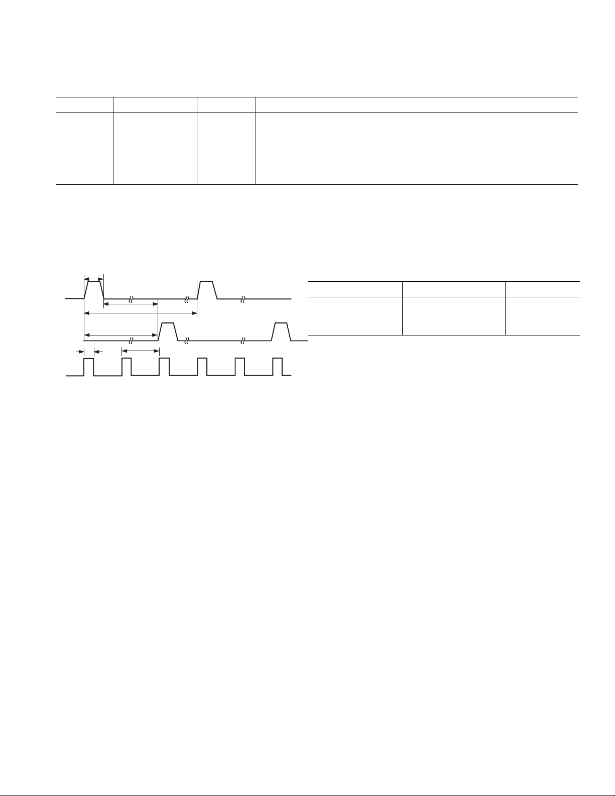
275 ms F1 and F2 Pulsewidth (Logic High)
See Table III sec Output Pulse Period. See Transfer Function Section
1/2 t
2
90 ms CF Pulsewidth (Logic High)
See Table IV sec CF Pulse Period. See Transfer Function Section
CLKIN/4 sec Minimum Time Between F1 and F2 Pulse
1, 2
T
to T
MIN
sec Time Between F1 Falling Edge and F2 Falling Edge
= –40ⴗC to +85ⴗC)
MAX
ADE7752
t
1
F1
t
t
6
2
t
F2
t
4
CF
3
t
5
Figure 1. Timing Diagram for Frequency Outputs
ORDERING GUIDE
Model Package Description Package Option
ADE7752AR SOIC Package R-24
EVAL-ADE7752EB ADE7752 Evaluation
Board
REV. PrB 08/01
3–
 Loading...