


Single-Phase Energy Measurement IC with
ADE5166/ADE5169/ADE5566/ADE5569
GENERAL FEATURES
Wide supply voltage operation: 2.4 V to 3.7 V
Internal bipolar switch between regulated and battery inputs
Ultralow power operation with power saving modes (PSM)
Full operation: 4.4 mA to 1.6 mA (PLL clock dependent)
Battery mode: 3.3 mA to 400 μA (PLL clock dependent)
Sleep mode
Real-time clock (RTC) mode: 1.7 μA
RTC and LCD mode: 38 μA (LCD charge pump enabled)
Reference: 1.2 V ± 0.1% (10 ppm/°C drift)
64-lead, low profile quad flat, RoHS-compliant package (LQFP)
Operating temperature range: −40°C to +85°C
ENERGY MEASUREMENT FEATURES
Proprietary analog-to-digital converters (ADCs) and digital
signal processing (DSP) provide high accuracy active
(watt), reactive (var), and apparent energy (volt-ampere
(VA)) measurement
<0.1% error on active energy over a dynamic range of
1000 to 1 @ 25°C
<0.5% error on reactive energy over a dynamic range of
1000 to 1 @ 25°C (ADE5169 and ADE5569 only)
<0.5% error on root mean square (rms) measurements
over a dynamic range of 500 to 1 for current (I
100 to 1 for voltage (V
Supports IEC 62053-21; IEC 62053-22; IEC 62053-23;
EN 50470-3 Class A, Class B, and Class C; and ANSI C12-16
Differential input with programmable gain amplifiers (PGAs)
supports shunts, current transformers, and di/dt current
sensors (ADE5169 and ADE5569 only)
2 current inputs for antitamper detection in the ADE5166/
ADE5169
High frequency outputs proportional to I
or apparent power (AP)
) @ 25°C
rms
, active, reactive,
rms
Table 1. Features Available on Each Part
Watt, VA,
Part No. Antitamper
ADE5166 Yes Yes No No
ADE5169 Yes Yes Yes Yes
ADE5566 No Yes No No
ADE5569 No Yes Yes Yes
I
, V
Var
rms
rms
) and
rms
di/dt
Sensor
8052 MCU, RTC, and LCD Driver
MICROPROCESSOR FEATURES
8052-based core
Single-cycle 4 MIPS 8052 core
8052-compatible instruction set
32.768 kHz external crystal with on-chip PLL
2 external interrupt sources
External reset pin
Low power battery mode
Wake-up from I/O, temperature change, alarm, and
universal asynchronous receiver/transmitter (UART)
LCD driver operation with automatic scrolling
Temperature measurement
Real-time clock (RTC)
Counter for seconds, minutes, hours, days, months,
and years
Date counter, including leap year compensation
Automatic battery switchover for RTC backup
Operation down to 2.4 V
Ultralow battery supply current: 1.7 μA
Selectable output frequency: 1 Hz to 16 kHz
Embedded digital crystal frequency compensation for
calibration and temperature variation of 2 ppm resolution
Integrated LCD driver
108-segment driver for the ADE5566 and ADE5569
104-segment driver for the ADE5166 and ADE5169
2×, 3×, or 4× multiplexing
4 LCD memory banks for screen scrolling
LCD voltages generated internally or with external resistors
Internal adjustable drive voltages up to 5 V independent
of power supply level
On-chip peripherals
2 independent UART interfaces
2
SPI or I
Watchdog timer
Power supply management with user-selectable levels
Memory: 62 kB flash memory, 2.256 kB RAM
Development tools
Single-pin emulation
IDE-based assembly and C source debugging
C
Rev. C
Information furnished by Analog Devices is believed to be accurate and reliable. However, no
responsibility is assumed by Analog Devices for its use, nor for any infringements of patents or other
rights of third parties that may result from its use. Specifications subject to change without notice. No
license is granted by implication or otherwise under any patent or patent rights of Analog Devices.
Trademarks and registered trademarks are the property of their respective owners.
One Technology Way, P.O. Box 9106, Norwood, MA 02062-9106, U.S.A.
Tel: 781.329.4700 www.analog.com
Fax: 781.461.3113 ©2008–2010 Analog Devices, Inc. All rights reserved.

ADE5166/ADE5169/ADE5566/ADE5569
TABLE OF CONTENTS
General Features ............................................................................... 1
Energy Measurement Features ........................................................ 1
Microprocessor Features .................................................................. 1
Revision History ............................................................................... 3
General Description ......................................................................... 4
Functional Block Diagrams ............................................................. 4
Specifications ..................................................................................... 6
Energy Metering ........................................................................... 6
Analog Peripherals ....................................................................... 7
Digital Interface ............................................................................ 8
Timing Specifications ................................................................ 10
Absolute Maximum Ratings .......................................................... 15
Thermal Resistance .................................................................... 15
ESD Caution ................................................................................ 15
Pin Configurations and Function Descriptions ......................... 16
Typical Performance Characteristics ........................................... 20
Terminology .................................................................................... 24
Special Function Register (SFR) Mapping .................................. 25
Power Management ........................................................................ 27
Power Management Register Details ....................................... 27
Power Supply Architecture ........................................................ 30
Battery Switchover ...................................................................... 30
Power Supply Management (PSM) Interrupt ......................... 30
Using the Power Supply Features ............................................. 32
Operating Modes ............................................................................ 35
PSM0 (Normal Mode) ............................................................... 35
PSM1 (Battery Mode) ................................................................ 35
PSM2 (Sleep Mode) .................................................................... 35
3.3 V Peripherals and Wake-Up Events ................................... 36
Transitioning Between Operating Modes ............................... 37
Using the Power Management Features .................................. 37
Energy Measurement ..................................................................... 38
Access to Energy Measurement SFRs ...................................... 38
Access to Internal Energy Measurement Registers ................ 38
Energy Measurement Registers ................................................ 41
Energy Measurement Internal Registers Details .................... 42
Interrupt Status/Enable SFRs .................................................... 45
Analog Inputs .............................................................................. 46
Analog-to-Digital Conversion .................................................. 47
Fault Detection (ADE5166/ADE5169 Only) .......................... 51
di/dt Current Sensor and Digital Integrator
(ADE5169/ADE5569 Only) ...................................................... 52
Power Quality Measurements ................................................... 53
Phase Compensation ................................................................. 55
RMS Calculation ........................................................................ 56
Active Power Calculation .......................................................... 58
Active Energy Calculation ........................................................ 61
Reactive Power Calculation (ADE5169/ADE5569 Only) ..... 64
Reactive Energy Calculation (ADE5169/ADE5569 Only) ... 66
Apparent Power Calculation ..................................................... 69
Apparent Energy Calculation ................................................... 69
Ampere-Hour Accumulation ................................................... 71
Energy-to-Frequency Conversion............................................ 72
Energy Register Scaling ............................................................. 72
Energy Measurement Interrupts .............................................. 73
Temperature, Battery, and Supply Voltage Measurements........ 74
Temperature Measurement ....................................................... 76
Battery Measurement ................................................................. 76
External Voltage Measurement ................................................ 77
8052 MCU Core Architecture....................................................... 79
MCU Registers ............................................................................ 79
Basic 8052 Registers ................................................................... 81
Standard 8052 SFRs .................................................................... 83
Memory Overview ..................................................................... 84
Addressing Modes ...................................................................... 85
Instruction Set ............................................................................ 86
Read-Modify-Write Instructions ............................................. 88
Instructions That Affect Flags .................................................. 89
Dual Data Pointers ......................................................................... 91
Interrupt System ............................................................................. 92
Standard 8052 Interrupt Architecture ..................................... 92
Interrupt Architecture ............................................................... 92
Interrupt Registers...................................................................... 92
Interrupt Priority ........................................................................ 93
Interrupt Flags ............................................................................ 94
Interrupt Vectors ........................................................................ 96
Interrupt Latency ........................................................................ 96
Context Saving ............................................................................ 96
Watchdog Timer ............................................................................. 97
Rev. C | Page 2 of 156

ADE5166/ADE5169/ADE5566/ADE5569
Writing to the Watchdog Timer SFR (WDCON, Address
0xC0) ............................................................................................. 98
Watchdog Timer Interrupt......................................................... 98
LCD Driver ...................................................................................... 99
LCD Registers .............................................................................. 99
LCD Setup ................................................................................. 102
LCD Timing and Waveforms ................................................. 102
Blink Mode ................................................................................ 103
Scrolling Mode ......................................................................... 103
Display Element Control ......................................................... 103
Voltage Generation .................................................................. 104
LCD External Circuitry ........................................................... 104
LCD Function in PSM2 Mode ............................................... 105
Flash Memory ............................................................................... 106
Flash Memory Overview ......................................................... 106
Flash Memory Organization ................................................... 106
Using the Flash Memory ......................................................... 107
Protecting the Flash Memory ................................................. 110
In-Circuit Programming ......................................................... 112
Timers ............................................................................................ 113
Timer Registers ......................................................................... 113
Timer 0 and Timer 1 ................................................................ 115
Timer 2 ...................................................................................... 116
PLL ................................................................................................. 118
PLL Registers ............................................................................ 118
Real-Time Clock (RTC) .............................................................. 119
Access to RTC SFRs ................................................................. 119
Access to Internal RTC Registers ........................................... 119
RTC SFRs .................................................................................. 120
RTC Registers ........................................................................... 123
RTC Calendar ........................................................................... 124
RTC Interrupts ......................................................................... 125
RTC Crystal Compensation .................................................... 126
UART Serial Interface ................................................................... 127
UART SFRs ................................................................................ 127
UART Operation Modes .......................................................... 130
UART Baud Rate Generation .................................................. 131
UART Additional Features ...................................................... 133
UART2 Serial Interface................................................................. 134
UART2 SFRs .............................................................................. 134
UART2 Operation Modes ........................................................ 136
UART2 Baud Rate Generation ................................................ 136
UART2 Additional Features .................................................... 137
Serial Peripheral Interface (SPI) .................................................. 138
SPI Registers .............................................................................. 138
SPI Pins ....................................................................................... 141
SPI Master Operating Modes .................................................. 142
SPI Interrupt and Status Flags ................................................. 143
I2C-Compatible Interface ............................................................. 144
Serial Clock Generation ........................................................... 144
Slave Addresses .......................................................................... 144
I2C Registers ............................................................................... 144
Read and Write Operations ..................................................... 145
I2C Receive and Transmit FIFOs ............................................. 146
I/O Ports ......................................................................................... 147
Parallel I/O ................................................................................. 147
I/O Registers .............................................................................. 148
Port 0 ........................................................................................... 151
Port 1 ........................................................................................... 151
Port 2 ........................................................................................... 151
Determining the Version of the
ADE5166/ADE5169/ADE5566/ADE5569 ................................ 152
Outline Dimensions ...................................................................... 153
Ordering Guide ......................................................................... 153
REVISION HISTORY
6/10—Rev. B to Rev. C
Changes to Bit 5, Table 161 .......................................................... 148
Changes to Ordering Guide ......................................................... 153
11/09—Rev. A to Rev. B
Deleted RTCCAL Function ......................................... Throughout
Changes to Fault Detection (ADE5166/ADE5169
Only) Section ................................................................................... 51
2/09—Rev. 0 to Rev. A
Added ADE5566/ADE5569 .............................................. Universal
Changes to General Features and Microprocessor Features ....... 1
Change to Figure 29, Figure 30, and Figure 31 ........................... 23
Rev. C | Page 3 of 156
Changes to Figure 46 ...................................................................... 49
Changes to Figure 59 ...................................................................... 56
Changes to Figure 61 ...................................................................... 57
Change to Figure 73 ........................................................................ 67
Changes to Figure 89 ...................................................................... 95
Changes to Figure 103 .................................................................. 120
Changes to Determining the Version of the
ADE5166/ADE5169/ADE5566/ADE5569 Section .................. 152
Changes to Ordering Guide ......................................................... 153
10/08—Revision 0: Initial Version
ADE5166/ADE5169/ADE5566/ADE5569
A
GENERAL DESCRIPTION
The ADE5166/ADE5169/ADE5566/ADE55691 integrate the
Analog Devices, Inc., energy (ADE) metering IC analog front
end and fixed function DSP solution with an enhanced 8052 MCU
core, a full RTC, an LCD driver, and all the peripherals to make
an electronic energy meter with an LCD display in a single part.
The ADE measurement core includes active, reactive, and apparent
energy calculations, as well as voltage and current rms measurements. This information is accessible for energy billing by using the
built-in energy scalars. Many power line supervisory features such
as SAG, peak, and zero crossing are included in the energy
measurement DSP to simplify energy meter design.
1
Patents pending.
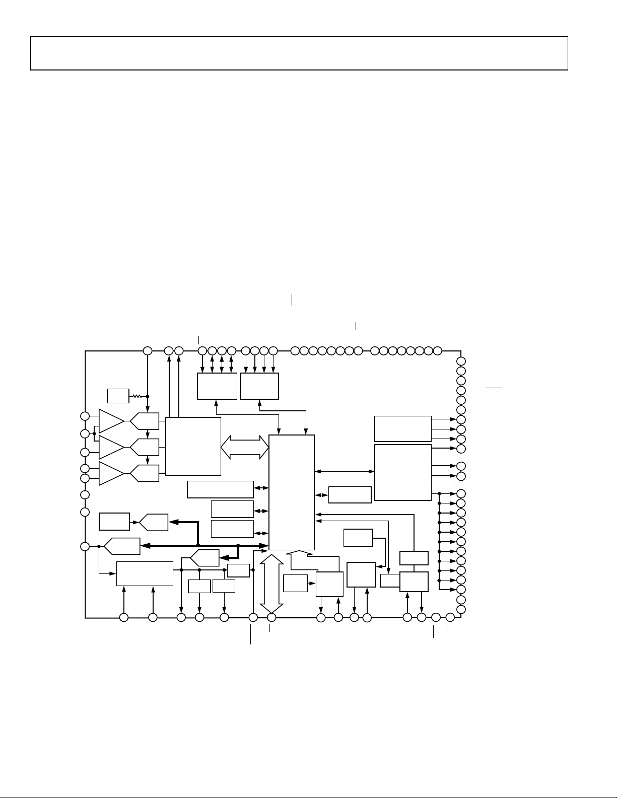
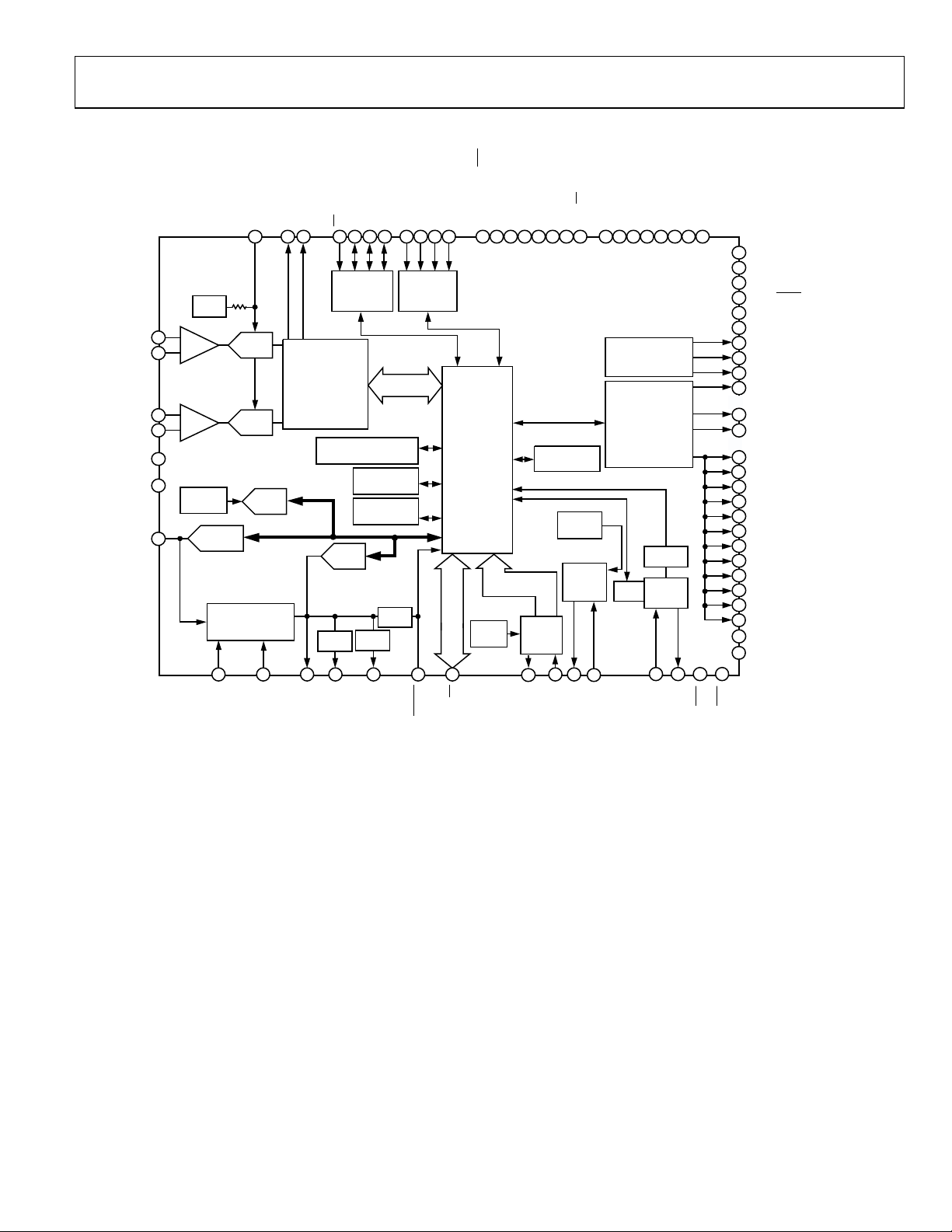
FUNCTIONAL BLOCK DIAGRAMS
The microprocessor functionality includes a single-cycle 8052 core,
a full RTC with a power supply backup pin, an SPI or I
2
C interface,
and two independent UART interfaces. The ready-to-use information from the ADE core reduces the requirement for program
memory size, making it easy to integrate complicated design into
62 kB of flash memory.
The ADE5166/ADE5169 include a 104-segment LCD driver and
the ADE5566/ADE5569 include a 108-segment LCD driver, each
with the capability to store up to four LCD screens in memory. This
driver generates voltages capable of driving LCDs up to 5 V.
TA
4/MOSI/SDA
P0.
TIMER
37
D
x
R
/MISO/ZX
P0.5
UART2
TIMER
UART2
SERIAL
44
2
/SCLK/T0
7/SS/T1/RxD
P0.
P0.6
PORT
2
D
x
T
P1.0/RxD
CHARGE PUMP
104-SEGMENT
LCD DRIVER
RTC
38
2
D
x
R
P24
/TxD
1.2/FP25/ ZX
P1.1
P
P1.3/T2EX/F
3V/5V LCD
2/FP23
P1.4/T
PLL
OSC
4647 48 45
1
L
A
T
X
/FP20
1.5/FP22
P1.6/FP21P1.7
P
12
P2.0/FP18
13
P2.1/FP17
14
P2.2/FP16
44
P2.3 (SDEN/P2.3/TxD2)
LCDVP1
19
LCDVP2
16
LCDVA
18
17
LCDVB
LCDVC
15
4
COM0
.
.
...
.
COM3
1
FP0
35
.
.
...
.
FP15
20
FP16
14
13
FP17
12
FP18
FP19
11
10
FP20
FP21
9
8
FP22
FP23
7
6
FP24
5
FP25
1
FP27
2
FP28
2
1
0
L
T
T
A
N
N
I
I
T
X
07411-201
I
I
DGND
GND
V
BAT
T1/P0.0)
A
K
L
C
S
S
S
SPI/I2C
SERIAL
USER RAM
256 BYTES
USER XRAM
LDO
59
O
S
I
M
2kB
A
T
N
I
V
T
A
D
S
/
I
S
O
M
POR
1
T2T
T0T
3 × 16-BIT
COUNTER
TIMERS
56
T
E
S
E
R
1-PIN
51
X
E
2
SINGLE
CYCLE
EMULATOR
EA
(BCTRL/IN
1/FP19
P0.0
P0.
8052
MCU
DOWNLOADER
DEBUGGER
UART
TIMER
2/CF1
.3/CF2
P0.
P0
ADE5166/ADE5169
WATCHDOG
UART
SERIAL
PORT
36
D
x
T
T
U
O
/
N
I
F
E
R
57
1.20V
REF
+
52
PA
PB
V
V
PGA1
–
53
I
N
+
PGA1
–
55
+
49
P
PGA2
–
50
N
63
54
TEMP
SENSOR
BATTERY
58
ADC
ADC
ADC
TEMP
ADC
ADC
POWER SUPPLY
CONTROL AND
MONIT ORING
64
60
N
I
C
D
V
2
1
F
F
C
C
43 42 39 38 7 6 45 11 43 42 41 40 39 38 37 36 5 6 7 8 9 1038 39 40 41
INTERFACE
ENERGY
MEASUREMENT
DSP
PROGRAM MEMORY
62kB FLASH
VSW
ADC
LDO
61
62
T
D
D
V
D
U
T
N
O
I
W
V
S
V
Figure 1. ADE5166/ADE5169 Functional Block Diagram
Rev. C | Page 4 of 156
ADE5166/ADE5169/ADE5566/ADE5569
A
)
A
K
L
C
S
S
S
SPI/I2C
SERIAL
USER RAM
256 BYTES
USER XRAM
LDO
T
A
D
S
/
I
O
S
S
I
O
1
T2T
T0T
M
M
3 × 16-BIT
COUNTER
TIMERS
2kB
POR
59
56
A
T
T
E
N
I
S
V
E
R
DGND
GND
V
BAT
T
U
O
/
N
I
F
E
R
57
1.20V
REF
+
52
I
P
PGA1
–
53
I
N
+
49
V
P
PGA2
–
50
V
N
63
54
TEMP
SENSOR
58
BATTERY
ADC
POWER SUPPLY
CONTROL AND
MONITORING
64
N
I
C
D
V
ADC
ADC
TEMP
ADC
2
1
F
F
C
C
43 42 39 38 7 6 45 11 43 42 41 40 39 38 37 36 5 6 7 8 9 1038 39 40 41
INTERFACE
ENERGY
MEASUREMENT
DSP
PROGRAM MEMORY
62kB FLASH
VSW
ADC
LDO
616062
T
D
D
V
D
U
T
N
O
I
W
V
S
V
X
E
2
1-PIN
51
EA
SINGLE
CYCLE
8052
MCU
EMULATOR
0
.
0
P
/
1
T
N
I
/
L
R
9
T
1
1
C
F
P
B
F
C
(
/
/
1
2
0
.
.
.
0
0
0
P
P
P
DOWNLOADER
DEBUGGER
UART
TIMER
A
2
T
D
A
x
0
D
X
R
T
Z
S
/
/
/
/
I
1
K
O
T
S
L
2
F
C
/
3
.
0
P
/
S
I
O
S
C
S
S
M
M
/
/
/
/
7
6
5
4
.
.
.
.
0
0
0
0
P
P
P
P
ADE5566/ADE5569
WATCHDOG
TIMER
UART2
TIMER
UART2
SERIAL
PORT
UART
SERIAL
PORT
44
37
36
2
D
D
x
D
x
x
T
R
T
D
x
R
/
0
.
1
P
CHARGE PUMP
108-SEGME NT
LCD DRIVER
RTC
38
2
D
x
R
4
2
P
X
F
Z
/
/
X
5
2
D
E
x
P
2
T
F
T
/
/
/
1
2
3
.
.
.
1
1
1
P
P
P
3V/5V LCD
3
2
P
2
F
2
/
2
P
T
F
/
/
4
5
.
.
1
1
P
P
PLL
OSC
4647 48 45
1
L
A
T
X
1
0
2
2
P
P
F
F
/
/
6
7
.
.
1
1
P
P
12
P2.0/FP18
13
P2.1/FP17
14
P2.2/FP16
44
P2.3 (SDEN/P2.3/TxD2)
19
LCDVP1
LCDVP2
16
LCDVA
18
17
LCDVB
LCDVC
15
4
COM0
.
.
...
.
COM3
1
FP0
35
.
.
...
.
FP15
20
FP16
14
13
FP17
12
FP18
FP19
11
10
FP20
FP21
9
8
FP22
FP23
7
6
FP24
5
FP25
55
FP26
1
FP27
2
FP28
2
1
0
L
T
T
A
N
N
I
I
T
X
07411-001
Figure 2. ADE5566/ADE5569 Functional Block Diagram
Rev. C | Page 5 of 156

ADE5166/ADE5169/ADE5566/ADE5569
SPECIFICATIONS
VDD = 3.3 V ± 5%, AGND = DGND = 0 V, on-chip reference XTALx = 32.768 kHz, T
ENERGY METERING
Table 2.
Parameter Min Typ Max Unit Test Conditions/Comments
MEASUREMENT ACCURACY1
Phase Error Between Channels
PF = 0.8 Capacitive ±0.05 Degrees Phase lead: 37°
PF = 0.5 Inductive ±0.05 Degrees Phase lag: 60°
Active Energy Measurement Error2 0.1 % of reading Over a dynamic range of 1000 to 1 at 25°C
AC Power Supply Rejection2 V
Output Frequency Variation 0.01 % IPx = VP = ±100 mV rms
DC Power Supply Rejection2 V
Output Frequency Variation 0.01 %
Active Energy Measurement Bandwidth1 8 kHz
Reactive Energy Measurement Error2 0.5 % of reading Over a dynamic range of 1000 to 1 at 25°C
V
Measurement Error2 0.5 % of reading Over a dynamic range of 100 to 1 at 25°C
rms
V
Measurement Bandwidth1 3.9 kHz
rms
I
Measurement Error2 0.5 % of reading Over a dynamic range of 500 to 1 at 25°C
rms
I
Measurement Bandwidth1 3.9 kHz
rms
ANALOG INPUTS
Maximum Signal Levels ±500 mV peak VP − VN differential input
ADE5166/ADE5169 ±500 mV peak IPA − IN and IPB − IN differential inputs
ADE5566/ADE5569 ±500 mV peak IP − IN
Input Impedance (DC) 770 kΩ
ADC Offset Error2 ±10 mV PGA1 = PGA2 = 1
±1 mV PGA1 = 16
Gain Error2
Current Channel ±3 % IPA = IPB = 0.5 V dc or IP = 0.5 V dc
Voltage Channel ±3 % VP − VN = 0.5 V dc
Gain Error Match ±0.2 %
CF1 AND CF2 PULSE OUTPUT
Maximum Output Frequency 21.6 kHz
Duty Cycle 50 % If the CF1 or CF2 frequency > 5.55 Hz
Active High Pulse Width 90 ms If the CF1 or CF2 frequency < 5.55 Hz
FAU LT D ETEC T ION3
Fault Detection Threshold
Inactive Input ≠ Active Input 6.25 % of active IPA or IPB active
Input Swap Threshold
Inactive Input > Active Input 6.25 % of active IPA or IPB active
Accuracy Fault Mode Operation
IPA Active, IPB = AGND 0.1 % of reading Over a dynamic range of 500 to 1
IPB Active, IPA = AGND 0.1 % of reading Over a dynamic range of 500 to 1
Fault Detection Delay 3 Seconds
Swap Delay 3 Seconds
1
These specifications are not production tested but are guaranteed by design and/or characterization data on production release.
2
See the Terminology section for definition.
3
Available only in the ADE5166/ADE5169.
MIN
to T
= −40°C to +85°C, unless otherwise noted.
MAX
= 3.3 V + 100 mV rms/120 Hz
DD
= 3.3 V ± 117 mV dc
DD
− VN = 500 mV peak; IPA − IN = 500 mV for
V
P
the ADE5166/ADE5169; I
the ADE5566/ADE5569
− IN = 500 mV for
P
Rev. C | Page 6 of 156

ADE5166/ADE5169/ADE5566/ADE5569
ANALOG PERIPHERALS
Table 3.
Parameter Min Typ Max Unit Test Conditions/Comments
INTERNAL ADCs (BATTERY, TEMPERATURE, V
Power Supply Operating Range 2.4 3.7 V Measured on V
No Missing Codes1 8 Bits
Conversion Delay2 38 μs
ADC Gain
V
Measurement 15.3 mV/LSB
DCIN
V
Measurement 14.6 mV/LSB
BAT
Temperature Measurement 0.83 °C/LSB
ADC Offset
V
Measurement at 3 V 200 LSB
DCIN
V
Measurement at 3.7 V 246 LSB
BAT
Temperature Measurement at 25°C 123 LSB
V
Analog Input
DCIN
Maximum Signal Levels 0 3.3 V
Input Impedance (DC) 1 MΩ
Low V
Detection Threshold 1.09 1.2 1.27 V
DCIN
POWER-ON RESET (POR)
VDD POR
Detection Threshold 2.5 2.95 V
POR Active Timeout Period 33 ms
V
POR
SWOUT
Detection Threshold 1.8 2.2 V
POR Active Timeout Period 20 ms
V
POR
INTD
Detection Threshold 2.0 2.25 V
POR Active Timeout Period 16 ms
V
POR
INTA
Detection Threshold 2.0 2.25 V
POR Active Timeout Period 120 ms
BATTERY SWITCHOVER
Voltage Operating Range (V
VDD to V
Switching
BAT
) 2.4 3.7 V
SWOUT
Switching Threshold (VDD) 2.5 2.95 V
Switching Delay 10 ns When VDD to V
30 ms When VDD to V
V
to VDD Switching
BAT
Switching Threshold (VDD) 2.5 2.95 V
Switching Delay 30 ms Based on VDD > 2.75 V
V
to V
SWOUT
Leakage Current 10 nA V
BAT
LCD, CHARGE PUMP ACTIVE
Charge Pump Capacitance Between
LCDVP1 and LCDVP2
LCDVA, LCDVB, LCDVC Decoupling Capacitance 470 nF
LCDVA 0 1.9 V
LCDVB 0 3.8 V 1/3 bias mode
LCDVC 0 5.8 V 1/3 bias mode
V1 Segment Line Voltage LCDVA − 0.1 LCDVA V Current on segment line = −2 μA
V2 Segment Line Voltage LCDVB − 0.1
V3 Segment Line Voltage LCDVC − 0.1
DC Voltage Across Segment and COMx Pin 50 mV
)
DCIN
100 nF
Rev. C | Page 7 of 156
LCDVB V Current on segment line = −2 μA
LCDVC V Current on segment line = −2 μA
SWOUT
switch is activated by VDD
BAT
switch is activated by V
BAT
= 0 V, V
BAT
= 3.43 V, TA = 25°C
SWOUT
LCDVC − LCDVB, LCDVC − LCDVA, or
LCDVB − LCDVA
DCIN

ADE5166/ADE5169/ADE5566/ADE5569
Parameter Min Typ Max Unit Test Conditions/Comments
LCD, RESISTOR LADDER ACTIVE
Leakage Current ±20 nA 1/2 and 1/3 bias modes, no load
V1 Segment Line Voltage LCDVA − 0.1 LCDVA V Current on segment line = −2 μA
V2 Segment Line Voltage LCDVB − 0.1 LCDVB V Current on segment line = −2 μA
V3 Segment Line Voltage LCDVC − 0.1 LCDVC V Current on segment line = −2 μA
ON-CHIP REFERENCE Nominal 1.2035 V
Reference Error −2.2 +2.2 mV TA = 25°C, f
Power Supply Rejection 80 dB
Temperature Coefficient1 10 50 ppm/°C f
1
These specifications are not production tested but are guaranteed by design and/or characterization data on production release.
2
Delay between ADC conversion request and interrupt set.
= 1.024 MHz
CORE
DIGITAL INTERFACE
Table 4.
Parameter Min Typ Max Unit Test Conditions/Comments
LOGIC INPUTS1
All Inputs Except XTAL1, XTAL2, BCTRL,
, INT1, RESET
INT0
Input High Voltage, V
Input Low Voltage, V
2.0 V
INH
0.8 V
INL
BCTRL, INT0, INT1, RESET
Input High Voltage, V
Input Low Voltage, V
1.3 V
INH
0.8 V
INL
Input Currents
RESET
Port 0, Port 1, Port 2 ±100 nA
−3.75 −8.5 μA
Input Capacitance 10 pF All digital inputs
FLASH MEMORY
Endurance2 20,000 Cycles At 25°C
Data Retention3 20 Years TJ = 85°C
CRYSTAL OSCILLATOR4
Crystal Equivalent Series Resistance 30 50 kΩ
Crystal Frequency 32 32.768 33.5 kHz
XTAL1 Input Capacitance 12 pF
XTAL2 Output Capacitance 12 pF
MCU CLOCK RATE (f
) 4.096 MHz Crystal = 32.768 kHz and CD bits = 0b000
CORE
32 kHz Crystal = 32.768 kHz and CD bits = 0b111
LOGIC OUTPUTS
Output High Voltage, VOH 2.4 V VDD = 3.3 V ± 5%
I
80 μA
SOURCE
Output Low Voltage, V
I
2 mA
SINK
5
0.4 V VDD = 3.3 V ± 5%
OL
START-UP TIME6
PSM0 Power-On Time 880 ms VDD at 2.75 V to PSM0 code execution
From Power Saving Mode 1 (PSM1)
PSM1 to PSM0 130 ms VDD at 2.75 V to PSM0 code execution
From Power Saving Mode 2 (PSM2)
PSM2 to PSM1 48 ms Wake-up event to PSM1 code execution
PSM2 to PSM0 186 ms VDD at 2.75 V to PSM0 code execution
100 nA
RESET = V
Internal pull-up disabled, input = 0 V or
V
SWOUT
Internal pull-up enabled, input = 0 V,
= 3.3 V
V
SWOUT
= 1.024 MHz
CORE
= 3.3 V
SWOUT
Rev. C | Page 8 of 156

ADE5166/ADE5169/ADE5566/ADE5569
Parameter Min Typ Max Unit Test Conditions/Comments
POWER SUPPLY INPUTS
VDD 3.13 3.3 3.46 V
V
2.4 3.3 3.7 V
BAT
INTERNAL POWER SUPPLY SWITCH (V
V
to V
BAT
VDD to V
V
to/from VDD Switching Open Time 40 ns
BAT
On Resistance 12 Ω V
SWOUT
On Resistance 9 Ω VDD = 3.13 V
SWOUT
BCTRL State Change and Switch Delay 18 μs
V
Output Current Drive 6 mA
SWOUT
POWER SUPPLY OUTPUTS
V
2.3 2.70 V
INTA
V
2.3 2.70 V
INTD
V
Power Supply Rejection 60 dB
INTA
V
Power Supply Rejection 50 dB
INTD
POWER SUPPLY CURRENTS
Current in Normal Mode (PSM0) 4.4 5.3 mA f
2.2 mA f
1.6 mA f
3 3.9 mA
Current in Battery Mode (PSM1) 3.3 5.05 mA f
1 mA f
Current in Sleep Mode (PSM2) 38 μA
1.7 μA RTC only, TA = 25°C, V
1
Specifications guaranteed by design.
2
Endurance is qualified as per JEDEC Standard 22 Method A117 and measured at −40°C, +25°C, +85°C, and +125°C.
3
Retention lifetime equivalent at junction temperature (TJ) = 85°C as per JEDEC Standard 22 Method A117. Retention lifetime derates with junction temperature.
4
Recommended crystal specifications.
5
Test carried out with all the I/Os set to a low output level.
6
Delay between power supply valid and execution of first instruction by 8052 core.
)
SWOUT
= 2.4 V
BAT
= 4.096 MHz, LCD and meter active
CORE
= 1.024 MHz, LCD and meter active
CORE
= 32.768 kHz, LCD and meter active
CORE
= 4.096 MHz; metering ADC and DSP,
f
CORE
powered down
= 4.096 MHz, LCD active, V
CORE
= 1.024 MHz, LCD active
CORE
= 3.7 V
BAT
LCD active with charge pump at 3.3 V + RTC,
= 3.3 V
V
BAT
= 3.3 V
BAT
Rev. C | Page 9 of 156
ADE5166/ADE5169/ADE5566/ADE5569
V
–
V
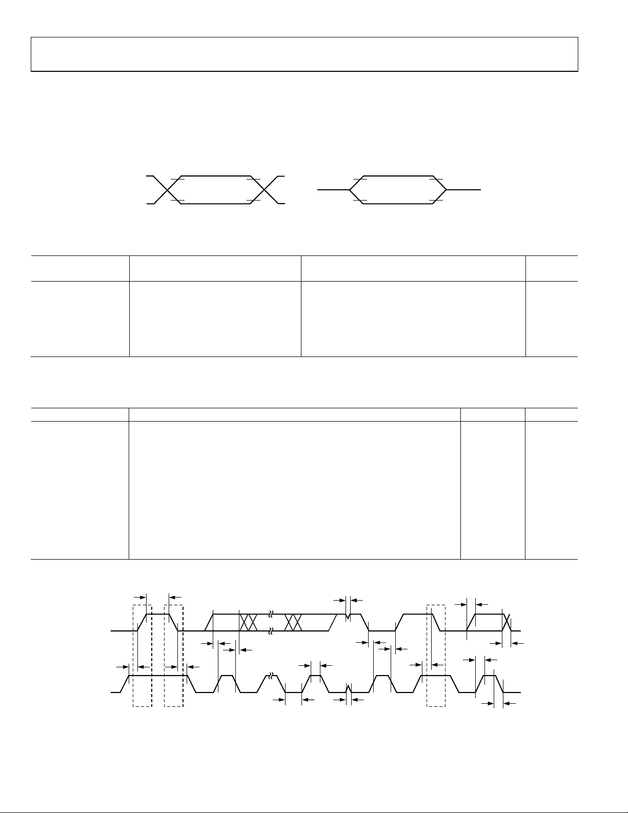
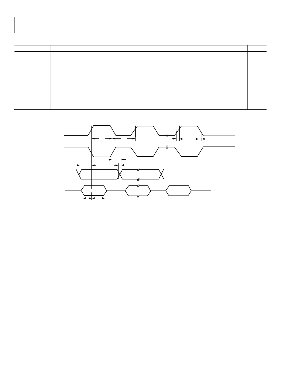
TIMING SPECIFICATIONS
AC inputs during testing were driven at V
and at 0.45 V for Logic 0. Timing measurements were made at V
minimum for Logic 1 and at V
maximum for Logic 0, as shown in
IL
Figure 3.
0.5
SWOUT
0.45V
Table 5. Clock Input (External Clock Driven XTAL1) Parameters
32.768 kHz External Crystal
Parameter Description Min Typ Max Unit
tCK XTAL1 period 30.52 μs
t
XTAL1 width low 6.26 μs
CKL
t
XTAL1 width high 6.26 μs
CKH
t
XTAL1 rise time 9 ns
CKR
t
XTAL1 fall time 9 ns
CKF
1/t
Core clock frequency1 1.024 MHz
CORE
1
The ADE5166/ADE5169/ADE5566/ADE5569 internal PLL locks onto a multiple (512×) of the 32.768 kHz external crystal frequency to provide a stable 4.096 MHz internal
clock for the system. The core can operate at this frequency or at a binary submultiple defined by the CD bits of the POWCON SFR, Address 0xC5[2:0] (see Tabl e 26).
− 0.5 V for Logic 1
SWOUT
0.2V
0.2V
+ 0.9V
SWOUT
TEST POINTS
– 0.1V
SWOUT
Figure 3. Timing Waveform Characteristics
IH
For timing purposes, a port pin is no longer floating when
a 100 mV change from load voltage occurs. A port pin begins
to float when a 100 mV change from the loaded V
occurs, as shown in Figure 3.
C
= 80 pF for all outputs, unless otherwise noted. VDD = 2.7 V
LOAD
to 3.6 V; all specifications T
V
– 0.1V
LOAD
V
LOAD
V
+ 0.1V
LOAD
TIMING
REFERENCE
POINTS
MIN
to T
V
LOAD
V
LOAD
, unless otherwise noted.
MAX
– 0.1V
V
LOAD
– 0.1V
07411-002
OH/VOL
level
Table 6. I2C-Compatible Interface Timing Parameters (400 kHz)
Parameter Description Typ Unit
t
Bus-free time between stop condition and start condition 1.3 μs
BUF
tL SCLK low pulse width 1.36 μs
tH SCLK high pulse width 1.14 μs
t
Start condition hold time 251.35 μs
SHD
t
Data setup time 740 ns
DSU
t
Data hold time 400 ns
DHD
t
Setup time for repeated start 12.5 ns
RSU
t
Stop condition setup time 400 ns
PSU
tR Rise time of both SCLK and SDATA 200 ns
tF Fall time of both SCLK and SDATA 300 ns
1
t
Pulse width of spike suppressed 50 ns
SUP
1
Input filtering on both the SCLK and SDATA suppresses noise spikes of <50 ns.
t
SDATA (I/O)
t
SCLK (I)
PSU
PS
STOP
CONDITI ON
BUF
START
CONDITI ON
MSB
t
DSU
t
SHD
1
t
DHD
Figure 4. I
2TO 7
2
C-Compatible Interface Timing
t
SUP
LSB ACK MSB
t
DSU
t
H
89 1
t
t
SUP
L
t
DHD
t
RSU
S(R)
REPEATED
START
t
R
t
F
t
t
F
R
07411-003
Rev. C | Page 10 of 156
ADE5166/ADE5169/ADE5566/ADE5569
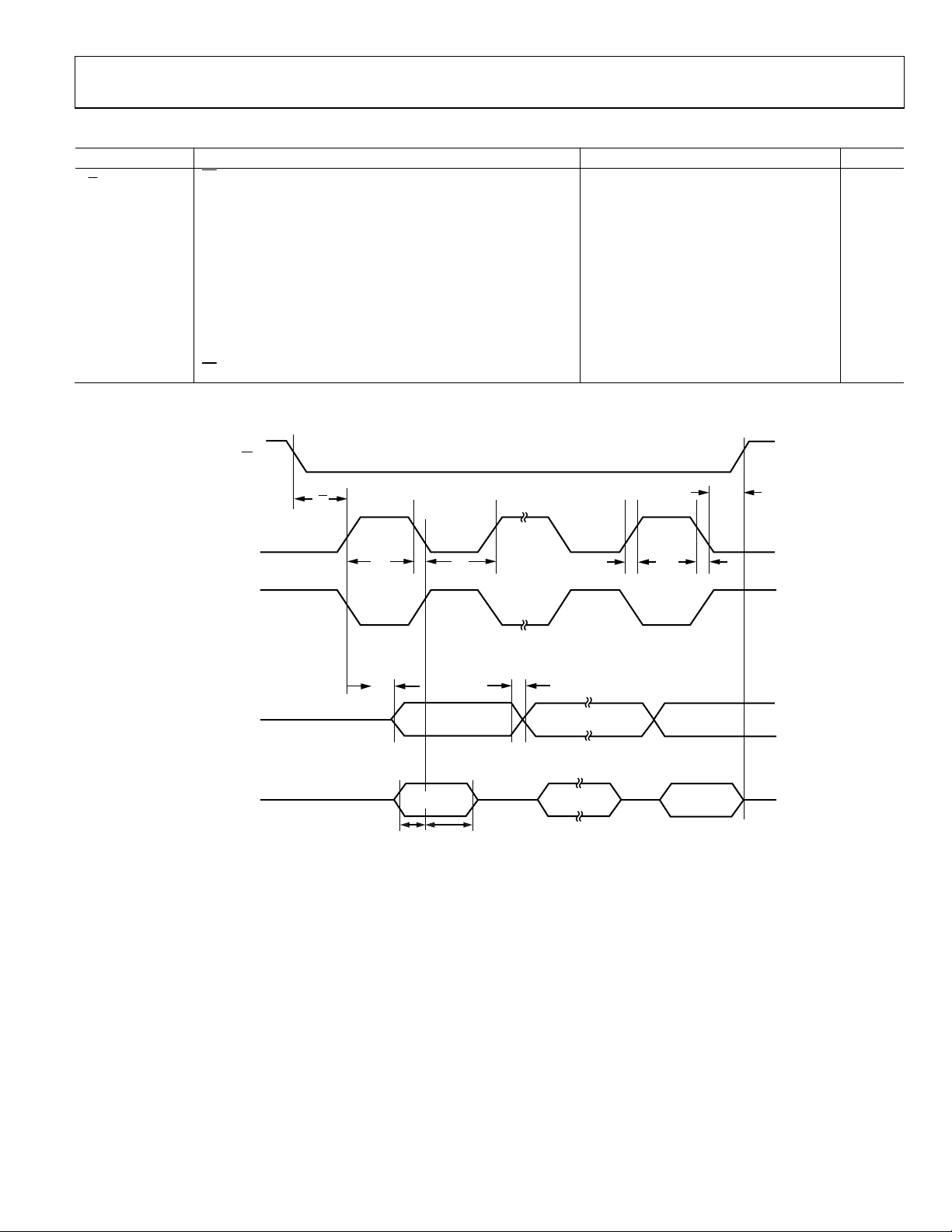
Table 7. SPI Master Mode Timing Parameters (SPICPHA = 1)
Parameter Description Min Typ Max Unit
tSL SCLK low pulse width 2
tSH SCLK high pulse width 2
t
Data output valid after SCLK edge 3 × t
DAV
t
Data input setup time before SCLK edge 0 ns
DSU
t
Data input hold time after SCLK edge t
DHD
tDF Data output fall time 19 ns
tDR Data output rise time 19 ns
tSR SCLK rise time 19 ns
tSF SCLK fall time 19 ns
1
t
depends on the clock divider or the CD bits of the POWCON SFR, Address 0xC5[2:0] (see Table 26); t
CORE
SCLK
(SPICPOL = 0)
SCLK
(SPICPOL = 1)
MOSI
t
SH
t
DAV
t
SL
MSB
t
DF
SPIR
SPIR
CORE
t
DR
BITS[6:1]
1
× t
ns
CORE
1
× t
ns
CORE
1
ns
= 2CD/4.096 MHz.
CORE
t
SR
t
SF
LSB
1
ns
CORE
MISO
MSB IN
t
t
DSU
DHD
BITS[ 6:1]
LSB IN
07411-004
Figure 5. SPI Master Mode Timing (SPICPHA = 1)
Rev. C | Page 11 of 156
ADE5166/ADE5169/ADE5566/ADE5569
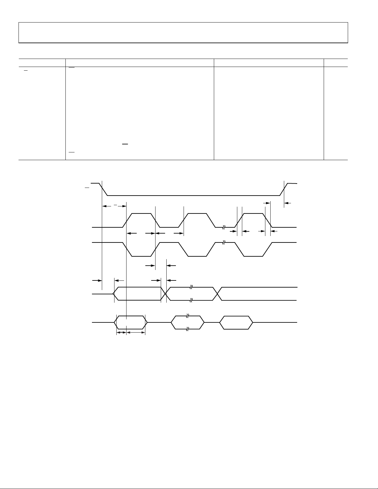
Table 8. SPI Master Mode Timing Parameters (SPICPHA = 0)
Parameter Description Min Typ Max Unit
tSL SCLK low pulse width 2
tSH SCLK high pulse width 2
t
Data output valid after SCLK edge 3 × t
DAV
t
Data output setup before SCLK edge 75 ns
DOSU
t
Data input setup time before SCLK edge 0 ns
DSU
t
Data input hold time after SCLK edge t
DHD
tDF Data output fall time 19 ns
tDR Data output rise time 19 ns
tSR SCLK rise time 19 ns
tSF SCLK fall time 19 ns
1
t
depends on the clock divider or the CD bits of the POWCON SFR, Address 0xC5[2:0] (see Table 26); t
CORE
SCLK
(SPICPOL = 0)
SCLK
(SPICPOL = 1)
MOSI
t
DOSU
MSB
t
SH
t
SL
t
DAV
t
DF
t
DR
BITS[6:1]
SPIR
SPIR
CORE
1
× t
(SPIR + 1) × t
CORE
1
× t
(SPIR + 1) × t
CORE
1
ns
= 2CD/4.096 MHz.
CORE
t
SR
LSB
t
SF
1
ns
CORE
1
ns
CORE
1
ns
CORE
MISO
t
DSU
MSB IN
t
BITS[6:1]
DHD
LSB IN
07411-005
Figure 6. SPI Master Mode Timing (SPICPHA = 0)
Rev. C | Page 12 of 156
ADE5166/ADE5169/ADE5566/ADE5569
Table 9. SPI Slave Mode Timing Parameters (SPICPHA = 1)
Parameter Description Min Typ Max Unit
tSS
to SCLK edge
SS
tSL SCLK low pulse width 6 × t
tSH SCLK high pulse width 6 × t
t
Data output valid after SCLK edge 25 ns
DAV
t
Data input setup time before SCLK edge 0 ns
DSU
t
Data input hold time after SCLK edge 2 × t
DHD
tDF Data output fall time 19 ns
tDR Data output rise time 19 ns
tSR SCLK rise time 19 ns
tSF SCLK fall time 19 ns
t
SFS
1
t
depends on the clock divider or the CD bits of the POWCON SFR, Address 0xC5[2:0] (see Table 26); t
CORE
high after SCLK edge
SS
SS
t
SS
145 ns
1
ns
CORE
1
ns
CORE
1
+ 0.5 μs
CORE
0 ns
= 2CD/4.096 MHz.
CORE
t
SFS
SCLK
(SPICPOL = 0)
SCLK
(SPICPOL = 1)
MISO
MOSI
t
t
SH
DAV
t
DSU
MSB IN
MSB
t
DHD
t
SL
t
SR
t
DF
t
DR
BITS[6:1]
BITS[6:1]
t
SF
LSB
LSB IN
07411-006
Figure 7. SPI Slave Mode Timing (SPICPHA = 1)
Rev. C | Page 13 of 156
ADE5166/ADE5169/ADE5566/ADE5569
Table 10. SPI Slave Mode Timing Parameters (SPICPHA = 0)
Parameter Description Min Typ Max Unit
tSS
to SCLK edge
SS
tSL SCLK low pulse width 6 × t
tSH SCLK high pulse width 6 × t
t
Data output valid after SCLK edge 25 ns
DAV
t
Data input setup time before SCLK edge 0 ns
DSU
t
Data input hold time after SCLK edge 2 × t
DHD
tDF Data output fall time 19 ns
tDR Data output rise time 19 ns
tSR SCLK rise time 19 ns
tSF SCLK fall time 19 ns
t
DOSS
t
SFS
1
t
depends on the clock divider or the CD bits of the POWCON SFR, Address 0xC5[2:0] (see Table 26); t
CORE
Data output valid after SS
high after SCLK edge
SS
edge
SS
t
SS
145 ns
1
ns
CORE
1
ns
CORE
1
+ 0.5 μs
CORE
0 ns
0 ns
= 2CD/4.096 MHz.
CORE
t
SFS
SCLK
(SPICPOL = 0)
SCLK
(SPICPOL = 1)
MISO
MOSI
t
DOSS
t
DSU
MSB IN
MSB
t
DHD
t
SH
t
DF
t
SL
t
DAV
t
DR
BITS[6:1]
BITS[6:1]
t
LSB IN
LSB
t
SF
07411-007
SR
Figure 8. SPI Slave Mode Timing (SPICPHA = 0)
Rev. C | Page 14 of 156
ADE5166/ADE5169/ADE5566/ADE5569
ABSOLUTE MAXIMUM RATINGS
TA = 25°C, unless otherwise noted.
Table 11.
Parameter Rating
VDD to DGND −0.3 V to +3.7 V
V
to DGND −0.3 V to +3.7 V
BAT
V
to DGND −0.3 V to V
DCIN
Input LCD Voltage to AGND, LCDVA,
LCDVB, LCDVC
1
Analog Input Voltage to AGND, VP, VN,
, IPB, and IN
I
P/IPA
−0.3 V to V
−2 V to +2 V
Digital Input Voltage to DGND −0.3 V to V
Digital Output Voltage to DGND −0.3 V to V
SWOUT
SWOUT
SWOUT
SWOUT
+ 0.3 V
+ 0.3 V
+ 0.3 V
+ 0.3 V
Operating Temperature Range (Industrial) −40°C to +85°C
Storage Temperature Range −65°C to +150°C
64-Lead LQFP, Power Dissipation
Lead Temperature (Soldering, 30 sec) 300°C
1
When used with external resistor divider.
Stresses above those listed under Absolute Maximum Ratings
may cause permanent damage to the device. This is a stress
rating only; functional operation of the device at these or any
other conditions above those indicated in the operational
section of this specification is not implied. Exposure to absolute
maximum rating conditions for extended periods may affect
device reliability.
THERMAL RESISTANCE
θJA is specified for the worst-case condition, that is, a device
soldered in a circuit board for surface-mount packages.
Table 12. Thermal Resistance
Package Type θJA θ
Unit
JC
64-Lead LQFP 60 20.5 °C/W
ESD CAUTION
Rev. C | Page 15 of 156
ADE5166/ADE5169/ADE5566/ADE5569
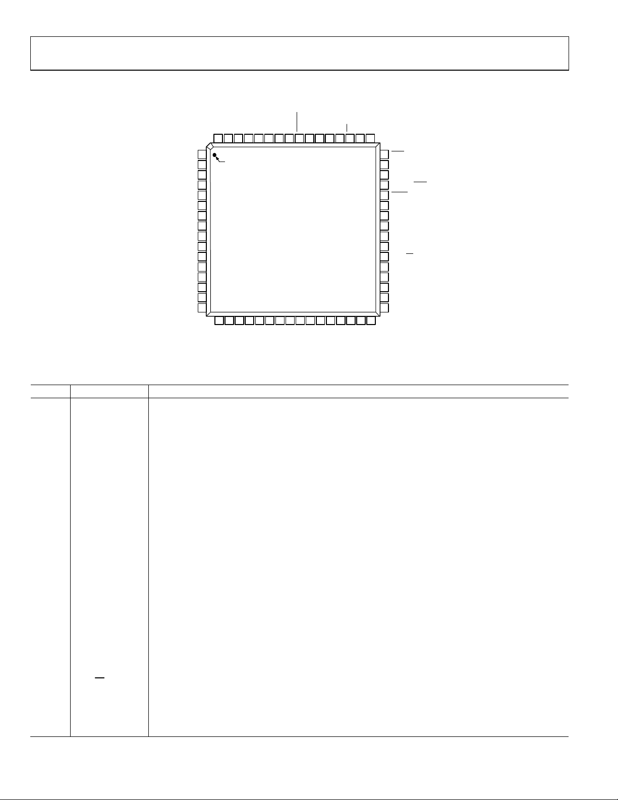
T
PIN CONFIGURATIONS AND FUNCTION DESCRIPTIONS
INTA
BAT
V
V
59
58
57
TOP VIEW
(Not to Scale)
24
IN/OU
PB
REF
I
AGND53I
RESET
56
55
54
25
26
FP927FP828FP729FP630FP531FP432FP3
FP11
FP10
N
51EA50
P
V
V
49
48
INT0
47
XTAL1
46
XTAL2
45
BCTRL/INT1/P0.0
44
SDEN/P2.3/TxD2
43
P0.2/CF1
42
P0.3/CF2
41
P0.4/MOSI/SDATA
40
P0.5/MISO/ZX
39
P0.6/SCLK/T0
38
P0.7/SS/T1/RxD2
37
P1.0/RxD
36
P1.1/TxD
35
FP0
34
FP1
33
FP2
07411-010
N
PA
I
52
COM3/F P27
COM2/F P28
COM1
COM0
P1.2/FP25/ZX
P1.3/T2EX/FP24
P1.4/T2/ FP23
P1.5/FP22
P1.6/FP21
P1.7/FP20
P0.1/FP19
P2.0/FP18
P2.1/FP17
P2.2/FP16
LCDVC
LCDVP2
DCIN
INTD
SWOUT
V
DGND62V
64
63
1
PIN 1
2
3
4
5
6
7
8
9
10
11
12
13
14
15
16
17
18
LCDVA
LCDVB
DD
V
V
61
60
ADE5166/ADE5169
19
20
FP1521FP1422FP1323FP12
LCDVP1
Figure 9. ADE5166/ADE5169 Pin Configuration
Table 13. Pin Function Descriptions
Pin No. Mnemonic Description
1 COM3/FP27 Common Output 3/LCD Segment Output 27. COM3 is used for the LCD backplane.
2 COM2/FP28 Common Output 2/LCD Segment Output 28. COM2 is used for the LCD backplane.
3 COM1 Common Output 1. COM1 is used for the LCD backplane.
4 COM0 Common Output 0. COM0 is used for the LCD backplane.
5 P1.2/FP25/ZX General-Purpose Digital I/O Port 1.2/LCD Segment Output 25/ZX Output.
6 P1.3/T2EX/FP24 General-Purpose Digital I/O Port 1.3/Timer 2 Control Input/LCD Segment Output 24.
7 P1.4/T2/FP23 General-Purpose Digital I/O Port 1.4/Timer 2 Input/LCD Segment Output 23.
8 P1.5/FP22 General-Purpose Digital I/O Port 1.5/LCD Segment Output 22.
9 P1.6/FP21 General-Purpose Digital I/O Port 1.6/LCD Segment Output 21.
10 P1.7/FP20 General-Purpose Digital I/O Port 1.7/LCD Segment Output 20.
11 P0.1/FP19 General-Purpose Digital I/O Port 0.1/LCD Segment Output 19.
12 P2.0/FP18 General-Purpose Digital I/O Port 2.0/LCD Segment Output 18.
13 P2.1/FP17 General-Purpose Digital I/O Port 2.1/LCD Segment Output 17.
14 P2.2/FP16 General-Purpose Digital I/O Port 2.2/LCD Segment Output 16.
15 LCDVC Output Port for LCD Levels. This pin should be decoupled with a 470 nF capacitor.
16 LCDVP2
Analog Output. A 100 nF capacitor should be connected between this pin and LCDVP1 for the internal LCD
charge pump device.
17, 18 LCDVB, LCDVA Output Ports for LCD Levels. These pins should be decoupled with a 470 nF capacitor.
19 LCDVP1
Analog Output. A 100 nF capacitor should be connected between this pin and LCDVP2 for the internal LCD
charge pump device.
20 to 35 FP15 to FP0 LCD Segment Output 15 to LCD Segment Output 0.
36 P1.1/TxD General-Purpose Digital I/O Port 1.1/Transmitter Data Output (Asynchronous).
37 P1.0/RxD General-Purpose Digital I/O Port 1.0/Receive Data Input (Asynchronous).
38
/T1/RxD2 General-Purpose Digital I/O Port 0.7/Slave Select When SPI Is in Slave Mode/Timer 1 Input/Receive Data
P0.7/SS
Input 2 (Asynchronous).
39 P0.6/SCLK/T0 General-Purpose Digital I/O Port 0.6/Clock Output for I2C or SPI Port/Timer 0 Input.
40 P0.5/MISO/ZX General-Purpose Digital I/O Port 0.5/Data Input for SPI Port/ZX Output.
41 P0.4/MOSI/SDATA General-Purpose Digital I/O Port 0.4/Data Output for SPI Port/I2C-Compatible Data Line.
Rev. C | Page 16 of 156

ADE5166/ADE5169/ADE5566/ADE5569
Pin No. Mnemonic Description
42 P0.3/CF2
43 P0.2/CF1
44
45
/P2.3/TxD2 Serial Download Mode Enable/General-Purpose Digital Output Port 2.3/Transmitter Data Output 2
SDEN
BCTRL/INT1
/P0.0 Digital Input for Battery Control/External Interrupt Input 1/General-Purpose Digital I/O Port 0.0. This logic
46 XTAL2
47 XTAL1
48
INT0
49, 50 VP, VN
51
Input for Emulation. When held high, this input enables the device to fetch code from internal program
EA
52, 53 IPA, IN
54 AGND Ground Reference for Analog Circuitry.
55 IPB
56
57 REF
58 V
59 V
RESET
IN/OUT
BAT
INTA
60 VDD
61 V
62 V
SWOUT
INTD
63 DGND Ground Reference for Digital Circuitry.
64 V
DCIN
General-Purpose Digital I/O Port 0.3/Calibration Frequency Logic Output 2. The CF2 logic output gives
instantaneous active, reactive, or apparent power or I
information.
rms
General-Purpose Digital I/O Port 0.2/Calibration Frequency Logic Output 1. The CF1 logic output gives
instantaneous active, reactive, or apparent power or I
information.
rms
(Asynchronous). This pin is used to enable serial download mode through a resistor when pulled low on
power-up or reset. On reset, this pin momentarily becomes an input, and the status of the pin is sampled.
If there is no pull-down resistor in place, the pin momentarily goes high, and then user code is executed.
If the pin is pulled down on reset, the embedded serial download/debug kernel executes, and this pin remains
low during the internal program execution. After reset, this pin can be used as a digital output port pin (P2.3)
or as Transmitter Data Output 2 (asynchronous).
or V
input connects V
DD
BAT
to V
open, the connection between V
internally when set to logic high or logic low, respectively. When left
SWOUT
or V
BAT
and V
DD
is selected internally.
SWOUT
A crystal can be connected across this pin and XTAL1 (see the XTAL1 pin description) to provide a clock
source. The XTAL2 pin can drive one CMOS load when an external clock is supplied at XTAL1 or by the gate
oscillator circuit. An internal 6 pF capacitor is connected to this pin.
An external clock can be provided at this logic input. Alternatively, a tuning fork crystal can be connected
across XTAL1 and XTAL2 to provide a clock source. The clock frequency for specified operation is 32.768 kHz.
An internal 6 pF capacitor is connected to this pin.
External Interrupt Input 0.
Analog Inputs for Voltage Channel. These inputs are fully differential voltage inputs with a maximum
differential level of ±500 mV for specified operation. This channel also has an internal PGA.
memory locations. The ADE5166/ADE5169 do not support external code memory. This pin should not be left
floating.
Analog Inputs for Current Channel. These inputs are fully differential voltage inputs with a maximum
differential level of ±500 mV for specified operation. This channel also has an internal PGA.
Analog Input for Second Current Channel. This input is fully differential with a maximum differential level of
±500 mV, referred to I
for specified operation. This channel also has an internal PGA.
N
Reset Input, Active Low.
Access to On-Chip Voltage Reference. The on-chip reference has a nominal value of 1.2 V ± 0.1% and a typical
temperature coefficient of 50 ppm/°C maximum. This pin should be decoupled with a 1 μF capacitor in
parallel with a ceramic 100 nF capacitor.
Power Supply Input from the Battery with a 2.4 V to 3.7 V Range. This pin is connected internally to V
when
DD
the battery is selected as the power supply.
Access to On-Chip 2.5 V Analog LDO. No external active circuitry should be connected to this pin. This pin
should be decoupled with a 10 μF capacitor in parallel with a ceramic 100 nF capacitor.
3.3 V Power Supply Input from the Regulator. This pin is connected internally to V
when the regulator is
SWOUT
selected as the power supply. This pin should be decoupled with a 10 μF capacitor in parallel with a ceramic
100 nF capacitor.
3.3 V Power Supply Output. This pin provides the supply voltage for the LDOs and the internal circuitry. This
pin should be decoupled with a 10 μF capacitor in parallel with a ceramic 100 nF capacitor.
Access to On-Chip 2.5 V Digital LDO. No external active circuitry should be connected to this pin. This pin
should be decoupled with a 10 μF capacitor in parallel with a ceramic 100 nF capacitor.
Analog Input for DC Voltage Monitoring. The maximum input voltage on this pin is V
with respect to
SWOUT
AGND. This pin is used to monitor the preregulated dc voltage.
Rev. C | Page 17 of 156
ADE5166/ADE5169/ADE5566/ADE5569
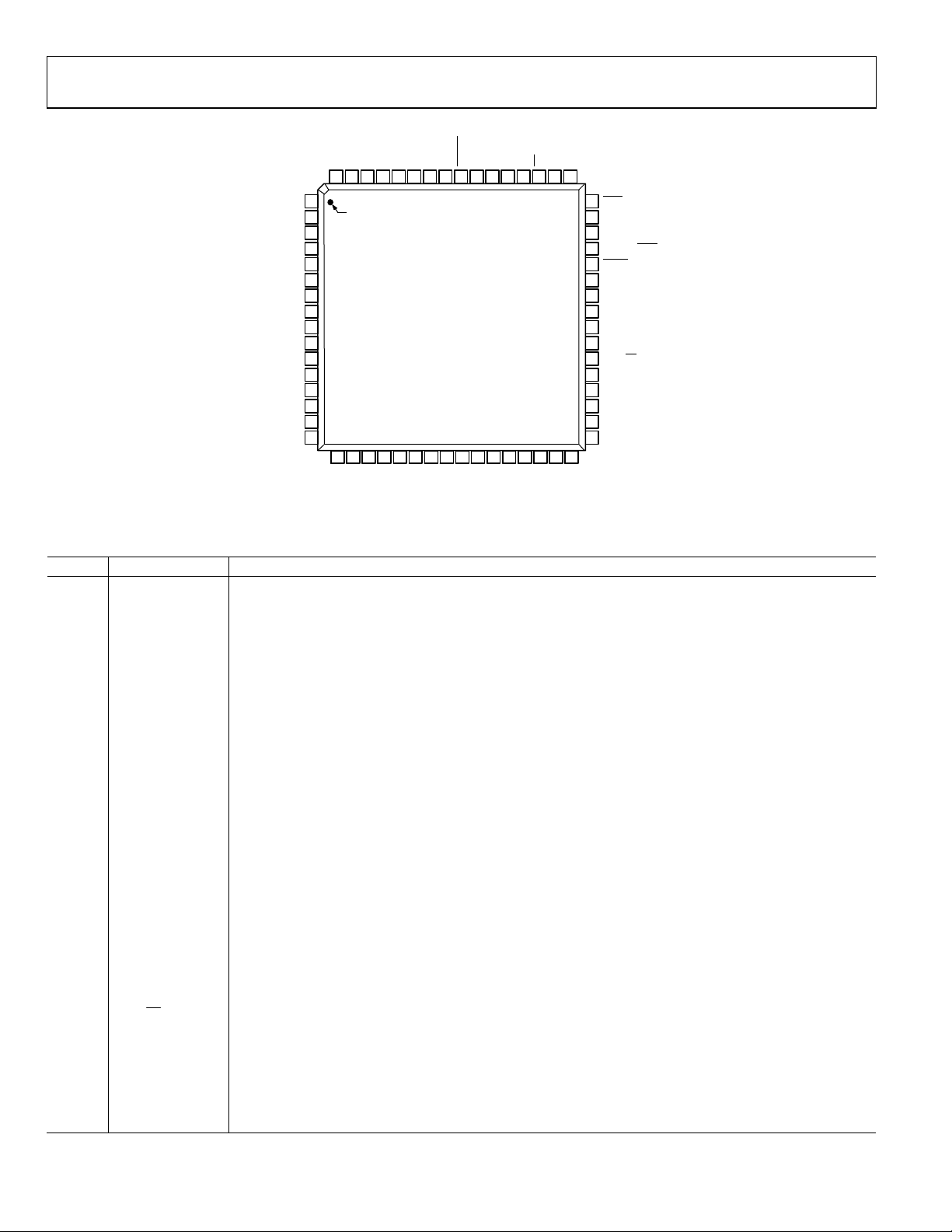
T
INTA
BAT
V
V
59
58
57
TOP VIEW
(Not to Scale)
24
IN/OU
FP26
REF
AGND53I
RESET
56 55
54
25
26
FP927FP828FP729FP630FP531FP432FP3
FP11
FP10
N
P
I
52 51EA50
N
P
V
V
49
48
INT0
47
XTAL1
46
XTAL2
45
BCTRL/INT1/P0.0
44
SDEN/P2.3/TxD2
43
P0.2/CF1
42
P0.3/CF2
41
P0.4/MOSI/SDATA
40
P0.5/MISO/ZX
39
P0.6/SCLK/T0
38
P0.7/SS/T1/RxD2
37
P1.0/RxD
36
P1.1/TxD
35
FP0
34
FP1
33
FP2
07411-028
COM3/F P27
COM2/F P28
COM1
COM0
P1.2/FP25/ZX
P1.3/T2EX/FP24
P1.4/T2/ FP23
P1.5/FP22
P1.6/FP21
P1.7/FP20
P0.1/FP19
P2.0/FP18
P2.1/FP17
P2.2/FP16
LCDVC
LCDVP2
DCIN
INTD
SWOUT
V
DGND62V
64
63
1
PIN 1
2
3
4
5
6
7
8
9
10
11
12
13
14
15
16
17
18
LCDVA
LCDVB
DD
V
V
61
60
ADE5566/ADE5569
19
20
FP1521FP1422FP1323FP12
LCDVP1
Figure 10. ADE5566/ADE5569 Pin Configuration
Table 14. Pin Function Descriptions
Pin No. Mnemonic Description
1 COM3/FP27 Common Output 3/LCD Segment Output 27. COM3 is used for the LCD backplane.
2 COM2/FP28 Common Output 2/LCD Segment Output 28. COM2 is used for the LCD backplane.
3 COM1 Common Output 1. COM1 is used for the LCD backplane.
4 COM0 Common Output 0. COM0 is used for the LCD backplane.
5 P1.2/FP25/ZX General-Purpose Digital I/O Port 1.2/LCD Segment Output 25/ZX Output.
6 P1.3/T2EX/FP24 General-Purpose Digital I/O Port 1.3/Timer 2 Control Input/LCD Segment Output 24.
7 P1.4/T2/FP23 General-Purpose Digital I/O Port 1.4/Timer 2 Input/LCD Segment Output 23.
8 P1.5/FP22 General-Purpose Digital I/O Port 1.5/LCD Segment Output 22.
9 P1.6/FP21 General-Purpose Digital I/O Port 1.6/LCD Segment Output 21.
10 P1.7/FP20 General-Purpose Digital I/O Port 1.7/LCD Segment Output 20.
11 P0.1/FP19 General-Purpose Digital I/O Port 0.1/LCD Segment Output 19.
12 P2.0/FP18 General-Purpose Digital I/O Port 2.0/LCD Segment Output 18.
13 P2.1/FP17 General-Purpose Digital I/O Port 2.1/LCD Segment Output 17.
14 P2.2/FP16 General-Purpose Digital I/O Port 2.2/LCD Segment Output 16.
15 LCDVC Output Port for LCD Levels. This pin should be decoupled with a 470 nF capacitor.
16 LCDVP2
Analog Output. A 100 nF capacitor should be connected between this pin and LCDVP1 for the internal LCD
charge pump device.
17, 18 LCDVB, LCDVA Output Ports for LCD Levels. These pins should be decoupled with a 470 nF capacitor.
19 LCDVP1
Analog Output. A 100 nF capacitor should be connected between this pin and LCDVP2 for the internal LCD
charge pump device.
20 to 35 FP15 to FP0 LCD Segment Output 15 to LCD Segment Output 0.
36 P1.1/TxD General-Purpose Digital I/O Port 1.1/Transmitter Data Output (Asynchronous).
37 P1.0/RxD General-Purpose Digital I/O Port 1.0/Receive Data Input (Asynchronous).
38
/T1/RxD2 General-Purpose Digital I/O Port 0.7/Slave Select When SPI Is in Slave Mode/Timer 1 Input/Receive Data
P0.7/SS
Input 2 (Asynchronous).
39 P0.6/SCLK/T0 General-Purpose Digital I/O Port 0.6/Clock Output for I2C or SPI Port/Timer 0 Input.
40 P0.5/MISO/ZX General-Purpose Digital I/O Port 0.5/Data Input for SPI Port/ZX Output.
41 P0.4/MOSI/SDATA General-Purpose Digital I/O Port 0.4/Data Output for SPI Port/I2C-Compatible Data Line.
42 P0.3/CF2
General-Purpose Digital I/O Port 0.3/Calibration Frequency Logic Output 2. The CF2 logic output gives
instantaneous active, reactive, or apparent power or I
information.
rms
Rev. C | Page 18 of 156

ADE5166/ADE5169/ADE5566/ADE5569
Pin No. Mnemonic Description
43 P0.2/CF1
44
45
/P2.3/TxD2 Serial Download Mode Enable/General-Purpose Digital Output Port 2.3/Transmitter Data Output 2
SDEN
BCTRL/INT1
/P0.0 Digital Input for Battery Control/External Interrupt Input 1/General-Purpose Digital I/O Port 0.0. This logic
46 XTAL2
47 XTAL1
48
INT0
49, 50 VP, VN
51
Input for Emulation. When held high, this input enables the device to fetch code from internal program
EA
52, 53 IP, IN
54 AGND Ground Reference for Analog Circuitry.
55 FP26 LCD Segment Output 26.
56
57 REF
58 V
59 V
RESET
IN/OUT
BAT
INTA
60 VDD
61 V
62 V
SWOUT
INTD
63 DGND Ground Reference for Digital Circuitry.
64 V
DCIN
General-Purpose Digital I/O Port 0.2/Calibration Frequency Logic Output 1. The CF1 logic output gives
instantaneous active, reactive, or apparent power or I
information.
rms
(Asynchronous). This pin is used to enable serial download mode through a resistor when pulled low on
power-up or reset. On reset, this pin momentarily becomes an input, and the status of the pin is sampled.
If there is no pull-down resistor in place, the pin momentarily goes high, and then user code is executed.
If the pin is pulled down on reset, the embedded serial download/debug kernel executes, and this pin
remains low during the internal program execution. After reset, this pin can be used as a digital output port
pin (P2.3) or as Transmitter Data Output 2 (asynchronous).
input connects V
open, the connection between V
DD
or V
BAT
to V
internally when set to logic high or logic low, respectively. When left
SWOUT
or V
BAT
and V
DD
is selected internally.
SWOUT
A crystal can be connected across this pin and XTAL1 (see the XTAL1 pin description) to provide a clock
source. The XTAL2 pin can drive one CMOS load when an external clock is supplied at XTAL1 or by the gate
oscillator circuit. An internal 6 pF capacitor is connected to this pin.
An external clock can be provided at this logic input. Alternatively, a tuning fork crystal can be connected
across XTAL1 and XTAL2 to provide a clock source. The clock frequency for specified operation is 32.768 kHz.
An internal 6 pF capacitor is connected to this pin.
External Interrupt Input 0.
Analog Inputs for Voltage Channel. These inputs are fully differential voltage inputs with a maximum
differential level of ±500 mV for specified operation. This channel also has an internal PGA.
memory locations. The ADE5566/ADE5569 do not support external code memory. This pin should not be left
floating.
Analog Inputs for Current Channel. These inputs are fully differential voltage inputs with a maximum
differential level of ±500 mV for specified operation. This channel also has an internal PGA.
Reset Input, Active Low.
Access to On-Chip Voltage Reference. The on-chip reference has a nominal value of 1.2 V ± 0.1% and a typical
temperature coefficient of 50 ppm/°C maximum. This pin should be decoupled with a 1 μF capacitor in
parallel with a ceramic 100 nF capacitor.
Power Supply Input from the Battery with a 2.4 V to 3.7 V Range. This pin is connected internally to V
when
DD
the battery is selected as the power supply.
Access to On-Chip 2.5 V Analog LDO. No external active circuitry should be connected to this pin. This pin
should be decoupled with a 10 μF capacitor in parallel with a ceramic 100 nF capacitor.
3.3 V Power Supply Input from the Regulator. This pin is connected internally to V
when the regulator is
SWOUT
selected as the power supply. This pin should be decoupled with a 10 μF capacitor in parallel with a ceramic
100 nF capacitor.
3.3 V Power Supply Output. This pin provides the supply voltage for the LDOs and the internal circuitry. This
pin should be decoupled with a 10 μF capacitor in parallel with a ceramic 100 nF capacitor.
Access to On-Chip 2.5 V Digital LDO. No external active circuitry should be connected to this pin. This pin
should be decoupled with a 10 μF capacitor in parallel with a ceramic 100 nF capacitor.
Analog Input for DC Voltage Monitoring. The maximum input voltage on this pin is V
with respect to
SWOUT
AGND. This pin is used to monitor the preregulated dc voltage.
Rev. C | Page 19 of 156
ADE5166/ADE5169/ADE5566/ADE5569
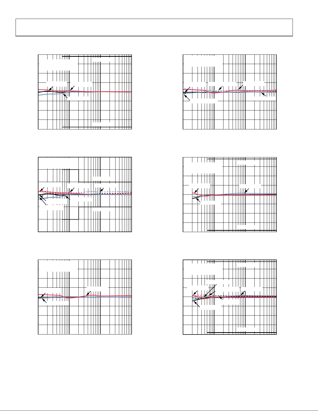
TYPICAL PERFORMANCE CHARACTERISTICS
2.0
GAIN = 1
1.5
INTEGRATOR OFF
INTERNAL REFERENCE
1.0
MID CLASS C
2.0
GAIN = 1
INTEGRATOR OFF
1.5
INTERNAL REFERENCE
1.0
0.5
+25°C; PF = 1
0
–0.5
ERROR (% of Reading)
–1.0
–1.5
–2.0
0.1 1 10 100
+85°C; PF = 1
–40°C; PF = 1
MID CLASS C
CURRENT CHANNEL (% of Full Scale)
Figure 11. Active Energy Error as a Percentage of Reading (Gain = 1)
over Temperature with Internal Reference, Integrator Off
1.5
GAIN = 1
INTEGRATOR OFF
INTERNAL REFERENCE
1.0
0.5
+85°C; PF = 1
0
+25°C; PF = 1
–0.5
+25°C; PF = 0.5
ERROR (% of Read ing)
–1.0
–1.5
0.1 1 10 100
+85°C; PF = 0.5
–40°C; PF = 1
CURRENT CHANNEL (% of Full Scale)
MID CLASS C
–40°C; PF = 0. 5
MID CLASS C
Figure 12. Active Energy Error as a Percentage of Reading (Gain = 1)
over Power Factor with Internal Reference, Integrator Off
2.0
GAIN = 1
INTEGRATOR OFF
1.5
INTERNAL REFERENCE
1.0
–0.5
ERROR (% of Reading)
–1.0
0.5
0
+25°C; PF = 0
–40°C; PF = 0
+85°C; PF = 0
0.5
+25°C; PF = 0
0
+25°C; PF = 0.866
–0.5
ERROR (% of Reading)
–1.0
–1.5
–2.0
0.1 1 10 100
07411-126
–40°C; PF = 0 .866
CURRENT CHANNEL (% of Full Scale)
+85°C; PF = 0
–40°C; PF = 0
07411-129
Figure 14. Reactive Energy Error as a Percentage of Reading (Gain = 1)
over Power Factor with Internal Reference, Integrator Off
2.0
GAIN = 1
1.5
INTEGRATOR OFF
INTERNAL REFERENCE
1.0
0.5
+85°C; PF = 1
0
–0.5
ERROR (% of Reading)
–1.0
–1.5
–2.0
0.1 1 10 100
07411-127
+25°C; PF = 1
CURRENT CHANNEL (% of Full Scale)
MID CLASS C
–40°C; PF = 1
MID CLASS C
07411-130
Figure 15. Current RMS Error as a Percentage of Reading (Gain = 1)
over Temperature with Internal Reference, Integrator Off
2.0
GAIN = 1
1.5
INTEGRATOR OFF
INTERNAL REFERENCE
1.0
0.5
+85°C; PF = 1
0
–0.5
ERROR (% of Read ing)
–1.0
–40°C; PF = 0. 5
+85°C; PF = 0.5
+25°C; PF = 0.5
+25°C; PF = 1
MID CLASS C
–40°C; PF = 1
–1.5
–2.0
0.1 1 10 100
CURRENT CHANNEL (% of Full Scale)
Figure 13. Reactive Energy Error as a Percentage of Reading (Gain = 1)
over Temperature with Internal Reference, Integrator Off
07411-128
Rev. C | Page 20 of 156
–1.5
–2.0
0.1 1 10 100
CURRENT CHANNEL (% of Full Scale)
MID CLASS C
Figure 16. Current RMS Error as a Percentage of Reading (Gain = 1)
over Power Factor with Internal Reference, Integrator Off
07411-131
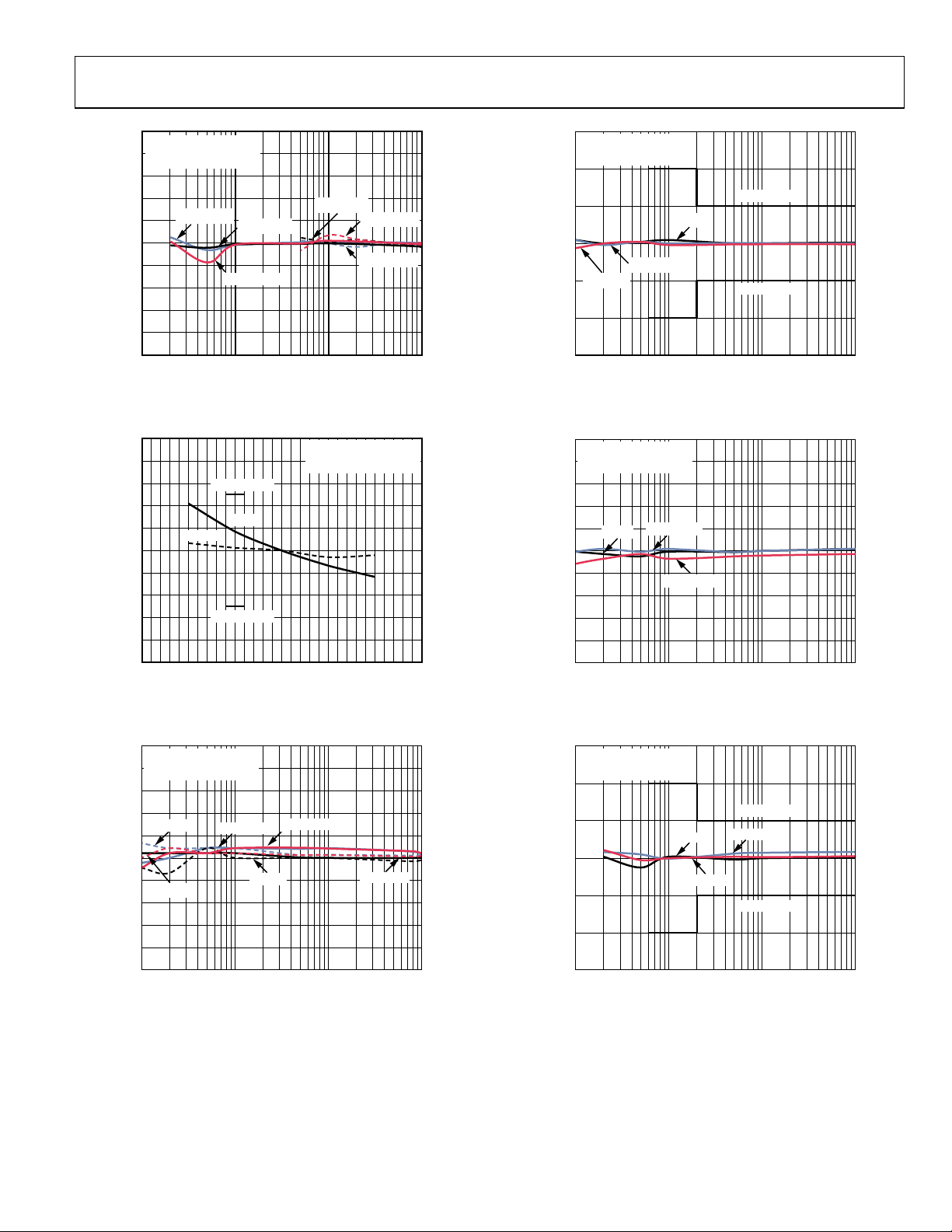
ADE5166/ADE5169/ADE5566/ADE5569
0.5
GAIN = 1
INTEGRATOR OFF
0.4
INTERNAL REFERENCE
0.3
0.2
I
; 3.13V
0.1
0
–0.1
–0.2
ERROR (% of Read ing)
–0.3
–0.4
–0.5
RMS
0.1 1 10 100
I
; 3.3V
RMS
I
; 3.43V
RMS
CURRENT CHANNEL (% of Full Scale)
V
; 3.3V
RMS
V
; 3.43V
RMS
V
; 3.13V
RMS
07411-132
Figure 17. Voltage and Current RMS Error as a Percentage of Reading
(Gain = 1) over Power Supply with Internal Reference
1.0
0.8
0.6
0.4
0.2
0
–0.2
–0.4
ERROR (% of Read ing)
–0.6
–0.8
–1.0
40 45 50 55 60 65 70
MID CLASS B
PF = 1
PF = 0.5
MID CLASS B
LINE FREQ UENCY (Hz)
GAIN = 1
INTEGRATOR OFF
INTERNAL REFERENCE
07411-133
Figure 18. Active Energy Error as a Percentage of Reading (Gain = 1)
over Frequency with Internal Reference, Integrator Off
0.5
GAIN = 1
INTEGRATOR OFF
0.4
INTERNAL REFE RENCE
0.3
0.2
W; 3.13V
0.1
0
–0.1
W; 3.43V
–0.2
ERROR (% of Reading)
–0.3
–0.4
–0.5
0.1 1 10 100
VAR; 3.13V
CURRENT CHANNEL (% of Full Scale)
W; 3.3V
VAR; 3.43V
VAR; 3.3V
07411-134
Figu re 19. Active and Reactive Energy Error as a Percentage of Reading (Gain = 1)
over Power Supply with Internal Reference, Integrator Off
1.5
GAIN = 8
INTEGRATOR OFF
INTERNAL REF ERENCE
1.0
0.5
0
PF = –0.5
–0.5
ERROR (% of Read ing)
–1.0
–1.5
0.1 1 10 100
PF = +1
PF = +0.5
CURRENT CHANNEL (% of Full Scale)
MID CLASS C
MID CLASS C
Figure 20. Active Energy Error as a Percentage of Reading (Gain = 8)
over Power Factor with Internal Reference, Integrator Off
1.0
GAIN = 8
INTEGRATOR OFF
0.8
INTERNAL REF ERENCE
0.6
0.4
0.2
0
–0.2
–0.4
ERROR (% of Read ing)
–0.6
–0.8
–1.0
0.1 1 10 100
PF = +0.866
PF = 0
PF = –0.866
CURRENT CHANNEL (% of Full Scale)
Figure 21. Reactive Energy Error as a Percentage of Reading (Gain = 8)
over Power Factor with Internal Reference, Integrator Off
1.5
GAIN = 8
INTEGRATOR OFF
INTERNAL REF ERENCE
1.0
0.5
PF = +1
0
–0.5
ERROR (% of Reading)
–1.0
–1.5
0.1 1 10 100
CURRENT CHANNEL (% of Full Scale)
PF = –0.5
MID CLASS C
PF = +0.5
MID CLASS C
Figure 22. Current RMS Error as a Percentage of Reading (Gain = 8)
over Power Factor with Internal Reference, Integrator Off
07411-135
07411-136
07411-137
Rev. C | Page 21 of 156
ADE5166/ADE5169/ADE5566/ADE5569
2.0
GAIN = 16
INTEGRATOR OFF
1.5
INTERNAL REF ERENCE
1.0
0.5
+25°C;PF = 1
0
–0.5
ERROR (% of Reading)
–1.0
–1.5
–2.0
0.1 1 10 100
–40°C;PF = 1
CURRENT CHANNEL (% of Full Scale)
MID CLASS C
+85°C;PF = 1
MID CLASS C
Figure 23. Active Energy Error as a Percentage of Reading (Gain = 16)
over Temperature with Internal Reference, Integrator Off
2.0
GAIN = 16
INTEGRATOR OFF
1.5
INTERNAL REFERENCE
1.0
+25°C;PF = 1
0.5
0
+85°C;PF = 1
MID CLASS C
–40°C;PF = 0.5
07411-138
1.0
GAIN = 16
INTEGRATOR OFF
0.8
INTERNAL REFERENCE
0.6
+85°C; PF = 0.866
0.4
0.2
0
–0.2
–0.4
ERROR (% of Reading)
–0.6
–0.8
–1.0
0.1 1 10 100
+85°C; PF = 0
CURRENT CHANNEL (% of Full Scale)
–40°C; PF = 0.866
+25°C; PF = 0
–40°C; PF = 0
+25°C; PF = 0.866
Figure 26. Reactive Energy Error as a Percentage of Reading (Gain = 16)
over Power Factor with Internal Reference, Integrator Off
2.0
GAIN = 16
INTEGRATOR OFF
1.5
INTERNAL REFERENCE
1.0
0.5
0
+85°C;PF = 1
MID CLASS C
07411-141
–0.5
ERROR (% of Read ing)
–1.0
–1.5
–2.0
0.1 1 10 100
–40°C;PF = 1
+85°C;PF = 0.5
CURRENT CHANNEL (% of Full Scale)
+25°C;PF = 0.5
MID CLASS C
Figure 24. Active Energy Error as a Percentage of Reading (Gain = 16)
over Power Factor with Internal Reference, Integrator Off
1.0
GAIN = 16
INTEGRATOR OFF
0.8
INTERNAL REFERENCE
0.6
0.4
0.2
0
–0.2
–0.4
ERROR (% of Read ing)
–0.6
–0.8
–1.0
0.1 1 10 100
+85°C; PF = 0
+25°C; PF = 0
CURRENT CHANNEL (% of Full Scale)
–40°C; PF = 0
Figure 25. Reactive Energy Error as a Percentage of Reading (Gain = 16)
over Temperature with Internal Reference, Integrator Off
–0.5
ERROR (% of Reading)
–1.0
–1.5
–2.0
0.1 1 10 100
07411-139
–40°C;PF = 1
+25°C;PF = 1
MID CLASS C
CURRENT CHANNEL (% of Fu ll Scale)
07411-142
Figure 27. Current RMS Error as a Percentage of Reading (Gain = 16)
over Temperature with Internal Reference, Integrator Off
2.0
GAIN = 16
INTEGRATOR OFF
1.5
INTERNAL REFERENCE
1.0
+85°C;PF = 1
0.5
0
–0.5
ERROR (% of Read ing)
–1.0
–1.5
–2.0
0.1 1 10 100
07411-140
+25°C;PF = 0.5
–40°C;PF = 1
+25°C;PF = 1
–40°C;PF = 0.5
CURRENT CHANNEL (% of Fu ll Scale)
MID CLASS C
+85°C;PF = 0.5
MID CLASS C
07411-143
Figure 28. Current RMS Error as a Percentage of Reading (Gain = 16)
over Power Factor with Internal Reference, Integrator Off
Rev. C | Page 22 of 156
ADE5166/ADE5169/ADE5566/ADE5569
2.0
GAIN = 16
INTEGRATOR ON
1.5
INTERNAL REFERENCE
1.0
–40°C;PF = 1
0.5
0
–0.5
ERROR (% of Read ing)
–1.0
+85°C;PF = 1
–40°C;PF = 0.5
+25°C; PF = 1
+25°C; PF = 0.5
MID CLASS C
+85°C;PF = 0.5
2.0
GAIN = 16
INTEGRATOR ON
1.5
INTERNAL REFERENCE
1.0
0.5
0
–0.5
ERROR (% of Reading)
–1.0
+25°C; PF = 0.5
+25°C; PF = 1
+85°C;PF = 1
–40°C; PF = 0 .5
–40°C; PF = 1
MID CLASS C
+85°C;PF = 0.5
–1.5
–2.0
0.1 1 10 100
CURRENT CHANNEL (% of Fu ll Scale)
MID CLASS C
Figure 29. Active Energy Error as a Percentage of Reading (Gain = 16)
over Power Factor with Internal Reference, Integrator On
1.0
GAIN = 16
INTEGRATOR ON
0.8
INTERNAL REFERENCE
0.6
+85°C; PF = 0.866
0.4
0.2
0
–0.2
–0.4
ERROR (% of Read ing)
–0.6
–0.8
–1.0
0.1 1 10 100
+85°C; PF = 0
+25°C; PF = 0
–40°C; PF = 0.866
CURRENT CHANNEL (% of Full Scale)
–40°C; PF = 0
+25°C; PF = 0.866
Figu re 30. Reactive Energy Error as a Percentage of Reading (Gain = 16)
over Power Factor with Internal Reference, Integrator On
–1.5
–2.0
0.1 1 10 100
07411-144
CURRENT CHANNEL (% of Fu ll Scale)
MID CLASS C
07411-146
Figure 31. Current RMS Error as a Percentage of Reading (Gain = 16)
over Power Factor with Internal Reference, Integrator On
07411-145
Rev. C | Page 23 of 156

ADE5166/ADE5169/ADE5566/ADE5569
TERMINOLOGY
Measurement Error
The error associated with the energy measurement made by the
ADE5166/ADE5169/ADE5566/ADE5569 is defined by the following formula:
Measurement Error =
⎛
⎜
⎜
⎝
Phase Error Between Channels
The digital integrator and the high-pass filter (HPF) in the current
channel have a nonideal phase response. To offset this phase
response and equalize the phase response between channels,
two phase correction networks are placed in the current channel:
one for the digital integrator and the other for the HPF. The phase
correction networks correct the phase response of the corresponding component and ensure a phase match between the
current channel and the voltage channel to within ±0.1° over a
range of 45 Hz to 65 Hz with the digital integrator off. With the
digital integrator on, the phase is corrected to within ±0.4° over
a range of 45 Hz to 65 Hz.
Power Supply Rejection (PSR)
PSR quantifies the ADE5166/ADE5169/ADE5566/ADE5569
measurement error as a percentage of reading when the power
supplies are varied. For the ac PSR measurement, a reading at
nominal supplies (3.3 V) is taken. A second reading is obtained
−
EnergyTrue
⎞
EnergyTrueRegisterEnergy
⎟
%100×
⎟
⎠
with the same input signal levels when an ac signal (100 mV rms/
120 Hz) is introduced onto the supplies. Any error introduced
by this ac signal is expressed as a percentage of the reading (see
the Measurement Error definition).
For the dc PSR measurement, a reading at nominal supplies
(3.3 V) is taken. A second reading is obtained with the same
input signal levels when the supplies are varied ±5%. Any error
introduced is expressed as a percentage of the reading.
ADC Offset Error
ADC offset error is the dc offset associated with the analog
inputs to the ADCs. It means that, with the analog inputs
connected to AGND, the ADCs still see a dc analog input
signal. The magnitude of the offset depends on the gain and
input range selection. However, when HPF1 is switched on,
the offset is removed from the current channel, and the power
calculation is not affected by this offset. The offsets can be
removed by performing an offset calibration (see the Analog
Inputs section).
Gain Error
Gain error is the difference between the measured ADC output
code (minus the offset) and the ideal output code (see the Current
Channel ADC section and the Voltage Channel ADC section).
It is measured for each of the gain settings on the current channel
(1, 2, 4, 8, and 16). The difference is expressed as a percentage
of the ideal code.
Rev. C | Page 24 of 156

ADE5166/ADE5169/ADE5566/ADE5569
SPECIAL FUNCTION REGISTER (SFR) MAPPING
Table 15. SFR Mapping
Mnemonic Address Description
INTPR 0xFF
Interrupt pins configuration SFR
(see Tab le 17).
SCRATCH4 0xFE Scratch Pad 4 (see Table 25 ).
SCRATCH3 0xFD Scratch Pad 3 (see Table 24).
SCRATCH2 0xFC Scratch Pad 2 (see Table 23).
SCRATCH1 0xFB Scratch Pad 1 (see Table 22 ).
BATVTH 0xFA
Battery detection threshold
(see Tab le 53).
STRBPER 0xF9
Peripheral ADC strobe period
(see Tab le 50).
IPSMF 0xF8
Power management interrupt flag
(see Tab le 18).
TEMPCAL 0xF7
RTC temperature compensation
(see Table 133).
RTCCOMP 0xF6
RTC nominal compensation
(see Table 132).
BATPR 0xF5
Battery switchover configuration
(see Tab le 19).
PERIPH 0xF4
Peripheral configuration
(see Tab le 20).
DIFFPROG 0xF3
Temperature and supply delta
(see Tab le 51).
B 0xF0 Auxiliary math (see Tabl e 57).
VDCINADC 0xEF V
SBAUD2 0xEE
ADC value (see Table 54).
DCIN
Enhanced Serial Baud Rate Control 2
(see Table 148).
LCDSEGE2 0xED LCD Segment Enable 2 (see Table 101).
IPSME 0xEC
Power management interrupt enable
(see Tab le 21).
SBUF2 0xEB Serial Port 2 buffer (see Table 14 7 ).
SPISTAT 0xEA SPI interrupt status (see Table 155).
SPI2CSTAT 0xEA I2C interrupt status (see Table 1 5 9).
SPIMOD2 0xE9 SPI Configuration SFR 2 (see Table 154).
I2CADR 0xE9 I2C slave address (see Table 158).
SPIMOD1 0xE8 SPI Configuration SFR 1 (see Table 153).
I2CMOD 0xE8 I2C mode (see Table 157).
WAV2H 0xE7 Selection 2 sample MSB (see Ta ble 31).
WAV2 M 0xE 6
Selection 2 sample middle byte
(see Tab le 31).
WAV2L 0xE5 Selection 2 sample LSB (see Table 31).
WAV1H 0xE4 Selection 1 sample MSB (see Ta ble 31).
WAV1 M 0xE 3
Selection 1 sample middle byte
(see Tab le 31).
WAV1L 0xE2 Selection 1 sample LSB (see Table 31).
SCON2 0xE1
Serial Communications Control 2
(see Table 146).
ACC 0xE0 Accumulator (see Table 57).
BATADC 0xDF Battery ADC value (see Table 5 5).
MIRQSTH 0xDE Interrupt Status 3 (see Tab le 43).
MIRQSTM 0xDD Interrupt Status 2 (see Table 42).
MIRQSTL 0xDC Interrupt Status 1 (see Table 41).
MIRQENH 0xDB Interrupt Enable 3 (see Tab le 46).
MIRQENM 0xDA Interrupt Enable 2 (see Table 45).
Rev. C | Page 25 of 156
Mnemonic Address Description
MIRQENL 0xD9 Interrupt Enable 1 (see Tab le 44).
ADCGO 0xD8 Start ADC measurement (see Table 52 ).
TEMPADC 0xD7 Temperature ADC value (see Table 56 ).
IRMSH 0xD6 I
IRMSM 0xD5
measurement MSB (see Table 31 ).
rms
measurement middle byte
I
rms
(see Tab le 31).
IRMSL 0xD4 I
VRMSH 0xD3 V
VRMSM 0xD2
measurement LSB (see Table 31 ).
rms
measurement MSB (see Table 31 ).
rms
measurement middle byte
V
rms
(see Tab le 31).
VRMSL 0xD1 V
measurement LSB (see Table 31 ).
rms
PSW 0xD0 Program status word (see Tab le 58).
TH2 0xCD Timer 2 high byte (see Table 120).
TL2 0xCC Timer 2 low byte (see Table 121).
RCAP2H 0xCB
Timer 2 reload/capture high byte
(see Table 122).
RCAP2L 0xCA
Timer 2 reload/capture low byte
(see Table 123).
T2CON 0xC8 Timer/Counter 2 control (see Table 115).
EADRH 0xC7 Flash high byte address (see Table 110).
EADRL 0xC6 Flash low byte address (see Table 109).
POWCON 0xC5 Power control (see Ta ble 26).
KYREG 0xC1 Key (see Tabl e 126).
WDCON 0xC0 Watchdog timer (see Tabl e 88).
STCON 0xBF Stack boundary (see Table 65).
EDATA 0xBC Flash data (see Table 108).
PROTKY 0xBB Flash protection key (see Tab le 107).
FLSHKY 0xBA Flash key (see Table 106).
ECON 0xB9 Flash control (see Table 105).
IP 0xB8 Interrupt priority (see Table 82 ).
SPH 0xB7 Stack pointer high (see Ta ble 64 ).
PINMAP2 0xB4
Port 2 weak pull-up enable
(see Table 164).
PINMAP1 0xB3
Port 1 weak pull-up enable
(see Table 163).
PINMAP0 0xB2
Port 0 weak pull-up enable
(see Table 162).
LCDCONY 0xB1 LCD Configuration Y (see Table 94 ).
CFG 0xAF Configuration (see Table 66).
LCDDAT 0xAE LCD data (see Table 100).
LCDPTR 0xAC LCD pointer (see Ta ble 99).
IEIP2 0xA9
Interrupt Enable and Priority 2
(see Tab le 83).
IE 0xA8 Interrupt enable (see Tab le 81).
DPCON 0xA7 Data pointer control (see Table 7 9).
RTCDAT 0xA4 RTC pointer data (see Table 131).
RTCPTR 0xA3 RTC pointer address (see Table 1 3 0).
TIMECON2 0xA2 RTC Configuration 2 (see Table 129).
TIMECON 0xA1 RTC configuration (see Table 128).
P2 0xA0 Port 2 (see Table 167).
EPCFG 0x9F
Extended port configuration
(see Table 161).

ADE5166/ADE5169/ADE5566/ADE5569
Mnemonic Address Description
SBAUDT 0x9E
SBAUDF 0x9D
LCDCONX 0x9C LCD Configuration X (see Table 9 2).
SPI2CRx 0x9B SPI/I2C receive buffer (see Table 152).
SPI2CTx 0x9A SPI/I2C transmit buffer (see Table 151).
SBUF 0x99 Serial port buffer (see Table 141).
SCON 0x98
LCDSEGE 0x97 LCD segment enable (see Table 98 ).
LCDCLK 0x96 LCD clock (see Table 95).
LCDCON 0x95 LCD configuration (see Tab le 91).
MDATH 0x94
MDATM 0x93
MDATL 0x92
Enhanced serial baud rate control
(see Table 142).
UART timer fractional divider
(see Table 143).
Serial communications control
(see Table 140).
Energy measurement pointer data MSB
(see Tab le 31).
Energy measurement pointer data
middle byte (see Table 31).
Energy measurement pointer data LSB
(see Tab le 31).
Mnemonic Address Description
MADDPT 0x91
P1 0x90 Port 1 (see Table 166).
TH1 0x8D Timer 1 high byte (see Table 118).
TH0 0x8C Timer 0 high byte (see Table 116).
TL1 0x8B Timer 1 low byte (see Table 119).
TL0 0x8A Timer 0 low byte (see Table 117).
TMOD 0x89
TCON 0x88
PCON 0x87 Program control (see Table 5 9).
DPH 0x83 Data pointer high (see Table 61 ).
DPL 0x82 Data pointer low (see Table 6 0).
SP 0x81 Stack pointer (see Tabl e 63).
P0 0x80 Port 0 (see Table 165).
Energy measurement pointer address
(see Tab le 30).
Timer/Counter 0 and Timer/Counter 1
mode (see Table 113).
Timer/Counter 0 and Timer/Counter 1
control (see Table 114).
Rev. C | Page 26 of 156
ADE5166/ADE5169/ADE5566/ADE5569
POWER MANAGEMENT
The ADE5166/ADE5169/ADE5566/ADE5569 have elaborate
power management circuitry that manages the regular power
supply to battery switchover and power supply failures.
Table 16. Power Management SFRs
SFR Address R/W Mnemonic Description
0xEC R/W IPSME Power management interrupt enable (see Tab le 21).
0xF5 R/W BATPR Battery switchover configuration (see Tabl e 19).
0xF8 R/W IPSMF Power management interrupt flag (see Table 18).
0xFF R/W INTPR Interrupt pins configuration (see Table 17).
0xF4 R/W PERIPH Peripheral configuration (see Table 20).
0xC5 R/W POWCON Power control (see Table 26).
0xFB R/W SCRATCH1 Scratch Pad 1 (see Table 2 2).
0xFC R/W SCRATCH2 Scratch Pad 2 (see Table 2 3).
0xFD R/W SCRATCH3 Scratch Pad 3 (see Table 24 ).
0xFE R/W SCRATCH4 Scratch Pad 4 (see Table 25 ).
POWER MANAGEMENT REGISTER DETAILS
Table 17. Interrupt Pins Configuration SFR (INTPR, Address 0xFF)
Bit Mnemonic Default Description
7 Reserved N/A Reserved.
[6:5] FSEL 00 Sets RTC calibration output frequency and calibration window.
FSEL Result (Calibration Window, Frequency)
00 30.5 sec, 1 Hz
01 30.5 sec, 512 Hz
10 0.244 sec, 500 Hz
11 0.244 sec, 16 kHz
4 Reserved N/A Reserved.
[3:1] INT1PRG 000
0 INT0PRG 0
1
X = don’t care
Controls the function of INT1
INT1PRG Result
X001 GPIO enabled
X011 BCTRL enabled
01X1
11X1
Controls the function of INT0
INT0PRG Result
0
1
INT1
INT1
INT0
INT0
Writing to the Interrupt Pins Configuration SFR (INTPR, Address 0xFF)
To protect the RTC from runaway code, a key must be written to the key SFR (KYREG, Address 0xC1) to obtain write access to the
INTPR SFR. The KYREG SFR (see Table 126) should be set to 0xEA to unlock the INTPR SFR and reset to 0 after a timekeeping register is
written to. The RTC registers can be written using the following 8052 assembly code:
MOV KYREG, #0EAh
MOV INTPR, #080h
.
input disabled
input enabled
.
input disabled
input enabled
The power management functionalities can be accessed directly
through the 8052 power management SFRs (see Table 1 6).
Rev. C | Page 27 of 156

ADE5166/ADE5169/ADE5566/ADE5569
Table 18. Power Management Interrupt Flag SFR (IPSMF, Address 0xF8)
Bit Bit Address Mnemonic Default Description
7 0xFF FPSR 0
Power supply restored interrupt flag. Set when the V
This occurs when the source of V
changes from V
SWOUT
6 0xFE FPSM 0 PSM interrupt flag. Set when an enabled PSM interrupt condition occurs.
5 0xFD FSAG 0 Voltage SAG interrupt flag. Set when an ADE energy measurement SAG condition occurs.
4 0xFC Reserved 0 This bit must be kept at 0 for proper operation.
3 0xFB FVADC 0
ADC monitor interrupt flag. Set when V
V
DCIN
DCIN
measurement is ready.
2 0xFA FBAT 0
monitor interrupt flag. Set when V
V
BAT
falls below BATVTH or when V
BAT
ready.
1 0xF9 FBSO 0 Battery switchover interrupt flag. Set when V
0 0xF8 FVDCIN 0 V
monitor interrupt flag. Set when V
DCIN
SWOUT
falls below 1.2 V.
DCIN
Table 19. Battery Switchover Configuration SFR (BATPR, Address 0xF5)
Bit Mnemonic Default Description
[7:2] Reserved 0 These bits must be kept at 0 for proper operation.
[1:0] BATPRG 0 Control bits for battery switchover.
BATPRG Result
00 Battery switchover enabled on low VDD
01 Battery switchover enabled on low VDD and low V
1X1 Battery switchover disabled
1
X = don’t care.
power supply has been restored.
DD
to VDD.
BAT
changes by VDCIN_DIFF or when the V
measurement is
BAT
switches from VDD to V
DCIN
BAT
.
DCIN
Table 20. Peripheral Configuration SFR (PERIPH, Address 0xF4)
Bit Mnemonic Default Description
7 RX2FLAG 0 If set, indicates that an RxD2 edge event has triggered wake-up from PSM2.
6 VSWSOURCE 1 Indicates the power supply that is internally connected to V
0 = V
1 = V
is connected to V
SWOUT
is connected VDD.
SWOUT
BAT
.
SWOUT
.
5 VDD_OK 1 If set, indicates that the VDD power supply is ready for operation.
4 PLL_FLT 0
If set, indicates that a PLL fault occurred where the PLL lost lock. Set the PLLACK bit (Bit 7) in the start
ADC measurement SFR (ADCGO, Address 0xD8) to acknowledge the fault and clear the PLL_FLT bit
(see Tab le 52).
3 REF_BAT_EN 0
Set this bit to enable the internal voltage reference in PSM2 mode. This bit should be set if LCD is on
in the PSM1 and PSM2 modes.
2 Reserved 0 This bit must be kept at 0 for proper operation.
[1:0] RXPROG 0
Controls the function of the P0.7/SS
/T1/RxD2 pin.
RXPROG Result
00 GPIO
01 RxD2 with wake-up disabled
11 RxD2 with wake-up enabled
Table 21. Power Management Interrupt Enable SFR (IPSME, Address 0xEC)
Bit Mnemonic Default Description
7 EPSR 0 Enables a PSM interrupt when the power supply restored interrupt flag (FPSR) is set.
6 Reserved 0 Reserved.
5 ESAG 0 Enables a PSM interrupt when the voltage SAG interrupt flag (FSAG) is set.
4 Reserved 0 This bit must be kept at 0 for proper operation.
3 EVADC 0 Enables a PSM interrupt when the V
2 EBAT 0 Enables a PSM interrupt when the V
ADC monitor interrupt flag (FVADC) is set.
DCIN
monitor interrupt flag (FBAT) is set.
BAT
1 EBSO 0 Enables a PSM interrupt when the battery switchover interrupt flag (FBSO) is set.
0 EVDCIN 0 Enables a PSM interrupt when the V
monitor interrupt flag (FVDCIN) is set.
DCIN
Rev. C | Page 28 of 156

ADE5166/ADE5169/ADE5566/ADE5569
Table 22. Scratch Pad 1 SFR (SCRATCH1, Address 0xFB)
Bit Mnemonic Default Description
[7:0] SCRATCH1 0 Value can be written/read in this register. This value is maintained in all the power saving modes.
Table 23. Scratch Pad 2 SFR (SCRATCH2, Address 0xFC)
Bit Mnemonic Default Description
[7:0] SCRATCH2 0 Value can be written/read in this register. This value is maintained in all the power saving modes.
Table 24. Scratch Pad 3 SFR (SCRATCH3, Address 0xFD)
Bit Mnemonic Default Description
[7:0] SCRATCH3 0 Value can be written/read in this register. This value is maintained in all the power saving modes.
Table 25. Scratch Pad 4 SFR (SCRATCH4, Address 0xFE)
Bit Mnemonic Default Description
[7:0] SCRATCH4 0 Value can be written/read in this register. This value is maintained in all the power saving modes.
Clearing the Scratch Pad Registers (SCRATCH1, Address 0xFB to SCRATCH4, Address 0xFE)
Note that these scratch pad registers are cleared only when the part loses VDD and V
Table 26. Power Control SFR (POWCON, Address 0xC5)
Bit Mnemonic Default Description
7 Reserved 1 Reserved.
6 METER_OFF 0
Set this bit to turn off the modulators and energy metering DSP circuitry to reduce power if metering
functions are not needed in PSM0 mode.
5 Reserved 0 This bit should be kept at 0 for proper operation.
4 COREOFF 0 Set this bit to shut down the core and enter PSM2 mode if in the PSM1 operating mode.
3 Reserved 0 Reserved.
[2:0] CD 010 Controls the core clock frequency, f
CD Result (f
CORE
CORE
. f
CORE
in MHz)
000 4.096
001 2.048
010 1.024
011 0.512
100 0.256
101 0.128
110 0.064
111 0.032
.
BAT
= 4.096 MHz/2CD.
Writing to the Power Control SFR (POWCON, Address 0xC5)
Writing data to the power control SFR (POWCON, Address 0xC5) involves writing 0xA7 into the key SFR (KYREG, Address 0xC1),
which is described in Table 126, followed by a write to the POWCON SFR. For example,
MOV KYREG,#0A7h ;Write KYREG to 0xA7 to get write access to the POWCON SFR
MOV POWCON,#10h ;Shut down the core
Rev. C | Page 29 of 156
ADE5166/ADE5169/ADE5566/ADE5569
V
V
POWER SUPPLY ARCHITECTURE
The ADE5166/ADE5169/ADE5566/ADE5569 have two power
supply inputs, V
supply at V
DD
and V
DD
for full operation. A battery backup, or secondary
. They require only a single 3.3 V power
BAT
power supply, with a maximum of 3.7 V can be connected to the
input. Internally, the ADE5166/ADE5169/ADE5566/
V
BAT
ADE5569 connect V
DD
or V
BAT
to V
, which is used to derive
SWOUT
power for the ADE5166/ADE5169/ADE5566/ADE5569 circuitry.
The V
supply (V
output pin reflects the voltage at the internal power
SWOUT
) and has a maximum output current of 6 mA. This
SWOUT
pin can also be used to power a limited number of peripheral components. The 2.5 V analog supply (V
the core logic (V
V
. Figure 32 shows the ADE5166/ADE5169/ADE5566/
SWOUT
) are derived by on-chip linear regulators from
INTD
) and the 2.5 V supply for
INTA
ADE5569 power supply architecture.
BCTRL
DCINVDDVBAT
POWER SUPPLY
MANAGEMENT
SCRATCH PAD LCD RTC
TEMPERATURE ADC
Figure 32. Power Supply Architecture
V
ADC
SW
ADC
SWOUT
LDO
LDO
V
INTD
V
3.3V
INTA
MCU
ADE
SPI/I2C
UART
2.5V
7411-011
The ADE5166/ADE5169/ADE5566/ADE5569 provide automatic
battery switchover between V
level detected at V
DD
or V
and V
DD
. In addition, the BCTRL input can be
DCIN
based on the voltage
BAT
used to trigger a battery switchover. The conditions for switching
V
from VDD to V
SWOUT
Battery Switchover section. V
and back to VDD are described in the
BAT
is an input pin that can be con-
DCIN
nected to a dc signal of 0 V to 3.3 V. This input is intended for
power supply supervisory purposes and does not provide power
to the ADE5166/ADE5169/ADE5566/ADE5569 circuitry (see
the Battery Switchover section).
BATTERY SWITCHOVER
The ADE5166/ADE5169/ADE5566/ADE5569 monitor VDD,
, and V
V
BAT
can be configured based on the status of the V
pin. Battery switchover is enabled by default. Setting Bit 1 in the
battery switchover configuration SFR (BATPR, Address 0xF5)
disables battery switchover so that V
V
(see Tabl e 19 ). The source of V
SWOUT
in the peripheral configuration SFR (PERIPH, Address 0xF4),
which is described in Ta bl e 2 0 . Bit 6 is set when V
nected to V
The battery switchover functionality provided by the ADE5166/
ADE5169/ADE5566/ADE5569 allows a seamless transition from
to V
V
DD
. Automatic battery switchover from VDD to V
DCIN
, V
DD
is always connected to
DD
is indicated by Bit 6
SWOUT
and cleared when V
DD
. An automatic battery switchover option ensures a
BAT
is connected to V
SWOUT
, or BCTRL
DCIN
is con-
SWOUT
BAT
BAT
.
stable power supply to the ADE5166/ADE5169/ADE5566/
ADE5569, as long as the external battery voltage is above 2.75 V.
It allows continuous code execution even while the internal power
supply is switching from V
metering ADCs are not available when V
DD
to V
and back. Note that the energy
BAT
is used for V
BAT
SWOUT
.
Power supply management (PSM) interrupts can be enabled to
indicate when battery switchover occurs and when the V
power
DD
supply is restored (see the Power Supply Management (PSM)
Interrupt section).
Switching from VDD to V
BAT
The following three events switch the internal power supply
(V
SWOUT
• V
from V
) from VDD to V
< 1.2 V. When V
DCIN
to V
DD
:
BAT
falls below 1.2 V, V
DCIN
. This event is enabled when the BATPRG
BAT
SWOUT
switches
bits (Bits[1:0]) in the battery switchover configuration SFR
(BATPR, Address 0xF5) are set to 0b01.
• V
< 2.75 V. When VDD falls below 2.75 V, V
DD
from V
DD
to V
. This event is enabled when the BATPRG
BAT
SWOUT
switches
bits in the BATPR SFR are cleared.
• Falling edge on BCTRL. When the battery control pin,
BCTRL, goes low, V
external switchover signal can trigger a switchover to V
switches from VDD to V
SWOUT
BAT
. This
BAT
at any time. Setting the INT1PRG bits (Bits[3:1]) to 0bX01 in
the interrupt pins configuration SFR (INTPR, Address 0xFF)
enables the BCTRL pin (see Tabl e 17 ).
Switching from V
To s wit c h V
SWOUT
to VDD
BAT
from V
to VDD, all of the following events
BAT
must be true:
• V
> 2.75 V. V
DD
switches back to VDD after VDD remains
SWOUT
above 2.75 V.
• V
> 1.2 V and VDD > 2.75 V. If the low V
DCIN
is enabled, V
above 1.2 V and V
switches to VDD after V
SWOUT
remains above 2.75 V.
DD
DCIN
DCIN
condition
remains
• Rising edge on BCTRL. If the battery control pin is enabled,
V
switches back to VDD after BCTRL is high, and the
SWOUT
first or second bullet point is satisfied.
POWER SUPPLY MANAGEMENT (PSM) INTERRUPT
The power supply management (PSM) interrupt alerts the 8052
core of power supply events. The PSM interrupt is disabled by
default. Setting Bit 1 (EPSM) in the Interrupt Enable and Priority 2
SFR (IEIP2, Address 0xA9) enables the PSM interrupt (see
Tabl e 83 ).
The power management interrupt enable SFR (IPSME,
Address 0xEC) controls the events that result in a PSM interrupt
(see Tabl e 21 ).
Figure 33 illustrates how the PSM interrupt vector is shared among
the PSM interrupt sources. The PSM interrupt flags are latched
and must be cleared by writing to the power management interrupt
flag SFR (IPSMF, Address 0xF8), as described in Ta b le 18 .
Rev. C | Page 30 of 156

ADE5166/ADE5169/ADE5566/ADE5569
IPSME ADDR. 0xEC
IPSMF ADDR. 0xF8
IEIP2 ADDR. 0xA9
EPSR
FPSR
ESAG
FSAG
EVADC
FVADC
EBAT
FBAT
EBSO
FBSO
EVDCIN
FVDCIN
FPSM
EPSM
EPSR RESERVED ESAG RESERVED EVADC EBAT EBSO EVDCIN
FPSR F PSM FSAG RESE RVED FVADC FBAT FBSO FVDCIN
PS2 P TI ES2 PSI EADE ETI EPSM ESI
NOT INVOLVED IN PSM INTERRUPT SIGNAL CHAIN
Figure 33. Power Supply Management Interrupt Sources
Battery Switchover and Power Supply Restored PSM Interrupt
The ADE5166/ADE5169/ADE5566/ADE5569 can be configured
to generate a PSM interrupt when the source of V
from V
DD
to V
, indicating battery switchover. Setting the EBSO
BAT
SWOUT
changes
bit (Bit 1) in the power management interrupt enable SFR (IPSME,
Address 0xEC) enables this event to generate a PSM interrupt
(see Tabl e 21 ).
The ADE5166/ADE5169/ADE5566/ADE5569 can also be configured to generate an interrupt when the source of V
from V
to VDD, indicating that the VDD power supply has been
BAT
SWOUT
changes
restored. Setting the EPSR bit (Bit 7) in the power management
interrupt enable SFR (IPSME, Address 0xEC) enables this event to
generate a PSM interrupt.
The flags in the IPSMF SFR for these interrupts, FBSO (Bit 1)
and FPSR (Bit 7), are set regardless of whether the respective
enable bits are set. The battery switchover and power supply
restore event flags (FBSO and FPSR) are latched. These events
must be cleared by writing 0 to these bits. The VSWSOURCE bit
(Bit 6) in the peripheral configuration SFR (PERIPH, Address
0xF4) tracks the source of V
connected to V
V
ADC PSM Interrupt
DCIN
and cleared when V
DD
. The bit is set when V
SWOUT
is connected to V
SWOUT
SWOUT
is
BAT
The ADE5166/ADE5169/ADE5566/ADE5569 can be configured
to generate a PSM interrupt when V
changes magnitude by
DCIN
more than a configurable threshold. This threshold is set in the
temperature and supply delta SFR (DIFFPROG, Address 0xF3),
as described in Tabl e 51. See the External Voltage Measurement
section for more information. Setting the EVADC bit (Bit 3) in
Rev. C | Page 31 of 156
TRUE?
PENDING PSM
INTERRUPT
07411-012
the power management interrupt enable SFR (IPSME, Address
0xEC) enables this event to generate a PSM interrupt.
The V
voltage is measured using a dedicated ADC. These
DCIN
measurements take place in the background at intervals to check
the change in V
. Conversions can also be initiated by writing to
DCIN
the start ADC measurement SFR (ADCGO, Address 0xD8), as
described in Ta ble 52. The FVADC flag indicates when a V
DCIN
measurement is ready. See the External Voltage Measurement
section for details on how V
V
Monitor PSM Interrupt
BAT
The V
voltage is measured using a dedicated ADC. These
BAT
is measured.
DCIN
measurements take place in the background at intervals to check
the change in V
. The FBAT bit (Bit 2 in the IPSMF SFR) is
BAT
set when the battery level is lower than the threshold set in the
battery detection threshold SFR (BATVTH, Address 0xFA),
described in Tab l e 5 3 ; or when a new measurement is ready in
the battery ADC value SFR (BATADC, Address 0xDF), described
in Tabl e 5 5 . See the Battery Measurement section for more information. Setting the EBAT bit (Bit 2) in the power management
interrupt enable SFR (IPSME, Address 0xEC) enables this event
to generate a PSM interrupt.
.
V
Monitor PSM Interrupt
DCIN
The V
voltage is monitored by a comparator. The FVDCIN
DCIN
bit (Bit 0) in the power management interrupt flag SFR (IPSMF,
Address 0xF8) is set when the V
input level is lower than 1.2 V.
DCIN
Setting the EVDCIN bit (Bit 0) in the IPSME SFR enables this
event to generate a PSM interrupt. This event, which is associated
with the SAG monitoring, can be used to detect that a power
supply (V
initiating a switch from V
) is compromised and to trigger further actions prior to
DD
to V
BAT
.
DD

ADE5166/ADE5169/ADE5566/ADE5569
SAG Monitor PSM Interrupt
The ADE5166/ADE5169/ADE5566/ADE5569 energy measurement DSP monitors the ac voltage input at the V
and VN input
P
pins. The SAGLVL register (Address 0x14) is used to set the threshold for a line voltage SAG event. The FSAG bit (Bit 5) in the
power management interrupt flag SFR (IPSMF, Address 0xF8)
is set if the line voltage stays below the level set in the SAGLVL
register for the number of line cycles set in the SAGCYC register
(Address 0x13). See the Line Voltage SAG Detection section
for more information. Setting the ESAG bit (Bit 5) in the power
management interrupt enable SFR (IPSME, Address 0xEC)
enables this event to generate a PSM interrupt.
USING THE POWER SUPPLY FEATURES
In an energy meter application, the 3.3 V power supply (VDD)
is typically generated from the ac line voltage and regulated to
3.3 V by a voltage regulator IC. The preregulated dc voltage,
typically 5 V to 12 V, can be connected to V
resistor divider. A 3.6 V battery can be connected to V
(240V, 220V, 110V TYPICAL)
AC INPUT
through a
DCIN
BAT
.
BCTRL
V
P
V
N
45
49
50
Figure 34 shows how the ADE5166/ADE5169/ADE5566/
ADE5569 power supply inputs are set up in this application.
Figure 35 shows the sequence of events that occurs if the main
power supply generated by the PSU starts to fail in the power
meter application shown in Figure 34. The SAG detection can
provide the earliest warning of a potential problem on V
When a SAG event occurs, user code can be configured to back
up data and prepare for battery switchover, if desired. The relative spacing of these interrupts depends on the design of the
power supply.
Figure 36 shows the sequence of events that occurs if the main
power supply starts to fail in the power meter application shown
in Figure 34, with battery switchover on low V
or low VDD
DCIN
enabled.
Finally, the transition between V
and V
DD
and the different
BAT
power supply modes (see the Operating Modes section) are
represented in Figure 37 and Figure 38.
SAG
DETECTIO N
DD
.
5V TO 12V DC
PSU
3.3V
REGULATOR
V
SWOUT
V
DCIN
64
V
DD
60
61
58
V
BAT
VO LTAGE
SUPERVISORY
VOLTAGE
SUPERVISORY
POWER SUPPLY
MANAGEMENT
Figure 34. Power Supply Management for Energy Meter Application
Table 27. Power Supply Event Timing Operating Modes
Parameter Time Description
t1 10 ns min Time between when V
goes below 1.2 V and when FVDCIN is raised.
DCIN
t2 10 ns min Time between when VDD falls below 2.75 V and when battery switchover occurs.
t3 30 ms typ
Time between when V
falls below 1.2 V and when battery switchover occurs if V
DCIN
battery switchover.
t4 130 ms typ
Time between when power supply restore conditions are met (V
bits = 0b01, or V
> 2.75 V if the BATPRG bits = 0b00) and when V
DD
> 1.2 V and VDD > 2.75 V if the BATPRG
DCIN
switches to VDD.
SWOUT
IPSMF SFR
(ADDR. 0xF8)
V
SW
is enabled to cause
DCIN
07411-013
Rev. C | Page 32 of 156

ADE5166/ADE5169/ADE5566/ADE5569
V
V
VP–
V
SAG LEVEL TRIP POINT
–
P
N
SAGCYC = 1
V
DCIN
1.2V
V
DD
2.75V
SAG EVENT
(FSAG = 1)
V
EVENT
DCIN
(FVDCIN = 1)
Figure 35. Power Supply Management Interrupts and Battery Switchover with Only V
t
1
t
2
IF SWITCHOVER ON LOW VDD IS ENABLED,
AUTOMATIC BAT TERY SWI TCHOVER OCCURS.
V
IS CONNECTED T O V
SWOUT
BSO EVENT
(FBSO = 1)
Enabled for Battery Switchover
DD
BAT
.
07411-014
N
SAG LEVEL TRIP POINT
SAGCYC = 1
V
DCIN
1.2V
t
3
t
DCIN
EVENT
DD
1
IF SWI TCHOVER ON L OW V
ENABLED, AUTO MATIC BATTERY
SWITCHOVER OCCURS. V
IS CONNECTED T O V
or V
Enabled for Battery Switchover
DCIN
BSO EVENT
(FBSO = 1)
DCIN
SWOUT
BAT
IS
.
07411-015
V
DD
2.75V
SAG EVENT
(FSAG = 1)
V
(FVDCIN = 1)
Figure 36. Power Supply Management Interrupts and Battery Switchover with V
Rev. C | Page 33 of 156

ADE5166/ADE5169/ADE5566/ADE5569
VP − V
N
SAG LEVEL
TRIP POINT
EVENT
V
DCIN
1.2V
V
2.75V
V
SWOUT
BATTERY SWITCH
ENABLED ON
LOW V
DCIN
V
SWOUT
BATTERY SWITCH
ENABLED ON
LOW V
DD
V
BAT
SAG EVENT
DD
PSM0 PSM0
PSM0 PSM0
V
DCIN
30ms
V
DCIN
PSM1 OR PSM2
PSM1 OR PSM2
EVENT
130ms
07411-016
Figure 37. Power Supply Management Transitions Between Modes
Rev. C | Page 34 of 156

ADE5166/ADE5169/ADE5566/ADE5569
OPERATING MODES
PSM0 (NORMAL MODE)
In PSM0 mode, or normal operating mode, V
. All of the analog circuitry and digital circuitry powered by
V
DD
V
and V
INTD
default clock frequency, f
are enabled by default. In normal mode, the
INTA
, which is established during a
CORE
power-on reset or software reset, is 1.024 MHz.
is connected to
SWOUT
PSM1 (BATTERY MODE)
In PSM1 mode, or battery mode, V
In this operating mode, the 8052 core and all of the digital circuitry
are enabled by default. The analog circuitry for the ADE energy
metering DSP powered by V
is disabled. This analog circuitry
INTA
automatically restarts, and the switch to the V
occurs when the V
supply is greater than 2.75 V and the
DD
PWRDN bit in the MODE1 register (Address 0x0B) is cleared
(see Tabl e 33 ). The default f
for PSM1, established during
CORE
a power-on reset or software reset, is 1.024 MHz.
is connected to V
SWOUT
DD
BAT
power supply
.
PSM2 (SLEEP MODE)
PSM2 mode is a low power consumption sleep mode for use
in battery operation. In this mode, V
All of the 2.5 V digital and analog circuitry powered through V
and V
is disabled, including the MCU core, resulting in the
INTD
following:
is connected to V
SWOUT
BAT
INTA
.
• The RAM in the MCU is no longer valid.
• The program counter for the 8052, also held in volatile
memory, becomes invalid when the 2.5 V supply is shut
down. Therefore, the program does not resume from where
it left off but always starts from the power-on reset vector
when the ADE5166/ADE5169/ADE5566/ADE5569 exit
PSM2 mode.
The 3.3 V peripherals (temperature ADC, V
ADC, RTC, and
DCIN
LCD) are active in PSM2 mode. They can be enabled or disabled
to reduce power consumption and are configured for PSM2
operation when the MCU core is active (see Table 2 9 for more
information about the individual peripherals and their PSM2
configuration). The ADE5166/ADE5169/ADE5566/ADE5569
remain in PSM2 mode until an event occurs to wake them up.
In PSM2 mode, the ADE5166/ADE5169/ADE5566/ADE5569
provide four scratch pad RAM SFRs that are maintained during
this mode. These SFRs can be used to save data from the PSM0
or PSM1 mode when entering PSM2 mode (see Tabl e 22 to
Tabl e 25 ).
In PSM2 mode, the ADE5166/ADE5169/ADE5566/ADE5569
maintain some SFRs (see Ta b le 2 8 ). The SFRs that are not listed
in this table should be restored when the part enters PSM0 or
PSM1 mode from PSM2 mode.
Table 28. SFRs Maintained in PSM2 Mode
I/O Configuration Power Supply Management RTC Peripherals LCD Peripherals
Interrupt pins configuration SFR
(INTPR, Address 0xFF);
see Tab le 17.
Peripheral configuration SFR
(PERIPH, Address 0xF4);
see Table 20.
Port 0 weak pull-up enable SFR
(PINMAP0, Address 0xB2);
see Table 162.
Port 1 weak pull-up enable SFR
(PINMAP1, Address 0xB3);
see Table 163.
Port 2 weak pull-up enable SFR
(PINMAP2, Address 0xB4);
see Table 164.
Scratch Pad 1 SFR (SCRATCH1,
Address 0xFB); see Table 22.
Battery detection threshold SFR
(BATVTH, Address 0xFA);
see Table 53.
Battery switchover configuration
SFR (BATPR, Address 0xF5);
see Table 19.
Battery ADC value SFR (BATADC,
Address 0xDF); see Table 55.
Peripheral ADC strobe period SFR
(STRBPER, Address 0xF9);
see Table 50.
Temperature and supply delta
SFR (DIFFPROG, Address 0xF3);
see Table 51.
V
ADC value SFR (VDCINADC,
DCIN
Address 0xEF); see Table 54.
RTC nominal compensation SFR
(RTCCOMP, Address 0xF6); see Table 132.
RTC temperature compensation SFR
(TEMPCAL, Address 0xF7); see Table 133.
RTC configuration SFR (TIMECON,
Address 0xA1); see Table 128.
RTC Configuration 2 SFR (TIMECON2,
Address 0xA2); see Table 129.
All indirectly accessible registers defined
in the RTC register list; see Table 1 34.
LCD Segment Enable 2 SFR
(LCDSEGE2, Address 0xED);
see Table 101.
LCD Configuration Y SFR
(LCDCONY, Address 0xB1);
see Table 94.
LCD Configuration X SFR
(LCDCONX, Address 0x9C);
see Table 92.
LCD configuration SFR
(LCDCON, Address 0x95);
see Table 91.
LCD clock SFR (LCDCLK,
Address 0x96); see Table 95 .
LCD segment enable SFR
(LCDSEGE, Address 0x97);
see Table 98.
Scratch Pad 2 SFR (SCRATCH2,
Address 0xFC); see Table 23 .
Temperature ADC value SFR
(TEMPADC, Address 0xD7);
LCD pointer SFR (LCDPTR,
Address 0xAC); see Table 9 9.
see Table 56.
Scratch Pad 3 SFR (SCRATCH3,
Address 0xFD); see Table 24.
Scratch Pad 4 SFR (SCRATCH4,
LCD data SFR (LCDDAT,
Address 0xAE); see Table 100.
Address 0xFE); see Table 25)
Rev. C | Page 35 of 156

ADE5166/ADE5169/ADE5566/ADE5569
3.3 V PERIPHERALS AND WAKE-UP EVENTS
Some of the 3.3 V peripherals are capable of waking the ADE5166/
ADE5169/ADE5566/ADE5569 from PSM2 mode. The events that
can cause the ADE5166/ADE5169/ADE5566/ADE5569 to wake
up from PSM2 mode are listed in the wake-up event column in
Table 29. 3.3 V Peripherals and Wake-Up Events
3.3 V
Peripheral
Temperature
Wake -Up
Event
Wake-Up
Enable Bits
Flag
Interrupt
Vec tor
∆T Maskable
ADC
V
ADC ΔV Maskable
DCIN
FVADC
IPSM
(IPSMF[3])
Power Supply
Management
RTC Interval Maskable
PSR Nonmaskable
FPSR
(IPSMF[7])
ITFLAG
IPSM
IRTC
(TIMECON[2])
Alarm Maskable
ALFLAG
IRTC
(TIMECON[6])
I/O Ports1
INT0PRG = 1
INT0
N/A IE0
(INTPR[0])
INT1PRG = 11x
INT1
N/A IE1
(INTPR[3:1])
Rx2 edge
RXPROG = 11
(PERIPH[1:0])
External
Reset Nonmaskable N/A N/A
RX2FLAG
(PERIPH[7])
N/A
Reset
LCD N/A N/A N/A N/A
Scratch Pad N/A N/A N/A N/A The four SCRATCHx registers remain intact in PSM2 mode.
1
All I/O pins are treated as inputs. The weak pull-up on each I/O pin can be disabled individually in the Port 0 weak pull-up enable SFR (PINMAP0, Address 0xB2), Port 1
weak pull-up enable SFR (PINMAP1, Address 0xB3), and Port 2 weak pull-up enable SFR (PINMAP2, Address 0xB4) to decrease current consumption. The interrupts can
be enabled or disabled.
Tabl e 29 . The interrupt flag associated with these events must
be cleared prior to executing instructions that put the ADE5166/
ADE5169/ADE5566/ADE5569 in PSM2 mode after wake-up.
Comments
The temperature ADC can wake up the ADE5166/ADE5169/
ADE5566/ADE5569. A pending interrupt is generated according
to the description in the Temperature Measurement section.
This wake-up event can be disabled by disabling temperature
measurements in the temperature and supply delta SFR
(DIFFPROG, Address 0xF3) in PSM2 mode. The temperature
interrupt needs to be serviced and acknowledged prior to
entering PSM2 mode.
The V
measurement can wake up the ADE5166/ADE5169/
DCIN
ADE5566/ADE5569. The FVADC flag, Bit 3 of the power management interrupt flag SFR (IPSMF, Address 0xF8), is set according to
the description in the External Voltage Measurement section.
This wake-up event can be disabled by clearing the EVADC bit,
Bit 3 in the power management interrupt enable SFR (IPSME,
Address 0xEC); see Table 2 1. The FVADC flag needs to be cleared
prior to entering PSM2 mode.
The ADE5166/ADE5169/ADE5566/ADE5569 wake up if the power
supply is restored (if V
switches to be connected to VDD). The
SWOUT
VSWSOURCE flag, Bit 6 of the peripheral configuration SFR (PERIPH,
Address 0xF4), is set to indicate that V
is connected to VDD.
SWOUT
The ADE5166/ADE5169/ADE5566/ADE5569 wake up after the
programmable time interval has elapsed. The RTC interrupt needs
to be serviced and acknowledged prior to entering PSM2 mode.
An alarm can be set to wake the ADE5166/ADE5169/ADE5566/
ADE5569 after the desired amount of time. The RTC alarm is
enabled by setting the ALxxx_EN bits in the RTC Configuration 2
SFR (TIMECON2, Address 0xA2). The RTC interrupt needs to be
serviced and acknowledged prior to entering PSM2 mode.
The edge of the interrupt is selected by the IT0 bit, Bit 0 in the
TCON SFR (TCON, Address 0x88). The IE0 flag, Bit 1 in the TCON
SFR, is not affected. The Interrupt 0 interrupt needs to be serviced
and acknowledged prior to entering PSM2 mode.
The edge of the interrupt is selected by the IT1 bit, Bit 2 in the
TCON SFR (TCON, Address 0x88). The IE1 flag, Bit 3 in the TCON
SFR, is not affected. The Interrupt 1 interrupt needs to be
serviced and acknowledged prior to entering PSM2 mode.
An Rx edge event occurs if a rising or falling edge is detected
on the RxD2 line. The UART2 RxD flag needs to be cleared prior
to entering PSM2 mode.
If the RESET
pin is brought low while the ADE5166/ADE5169/
ADE5566/ADE5569 are in PSM2 mode, they wake up to PSM1
mode.
The LCD can be enabled/disabled in PSM2 mode. The LCD data
memory remains intact.
Rev. C | Page 36 of 156

ADE5166/ADE5169/ADE5566/ADE5569
TRANSITIONING BETWEEN OPERATING MODES
The operating mode of the ADE5166/ADE5169/ADE5566/
ADE5569 is determined by the power supply connected to
. Therefore, changes in the power supply, such as when
V
SWOUT
V
switches from VDD to V
SWOUT
, alter the operating mode. This section describes events
V
DD
that change the operating mode.
Automatic Battery Switchover (PSM0 to PSM1)
If any of the enabled battery switchover events occurs (see the
Battery Switchover section), V
over results in a transition from PSM0 to PSM1 operating mode.
When battery switchover occurs, the analog circuitry used in
the ADE energy measurement DSP is disabled. To reduce power
consumption, user code can initiate a transition to PSM2 mode.
Entering Sleep Mode (PSM1 to PSM2)
To reduce power consumption when V
user code can initiate sleep mode, PSM2, by setting Bit 4 in the
power control SFR (POWCON, Address 0xC5) to shut down the
MCU core. Events capable of waking the MCU can be enabled
(see the 3.3 V Peripherals and Wake-Up Events section).
Servicing Wake-Up Events (PSM2 to PSM1)
The ADE5166/ADE5169/ADE5566/ADE5569 may need to
wake up from PSM2 mode to service wake-up events (see the
3.3 V Peripherals and Wake-Up Events section). PSM1 code
execution begins at the power-on reset vector. After servicing
the wake-up event, the ADE5166/ADE5169/ADE5566/ADE5569
can return to PSM2 mode by setting Bit 4 in the power control SFR
(POWCON, Address 0xC5) to shut down the MCU core.
Automatic Switch to VDD (PSM2 to PSM0)
If the conditions to switch V
Battery Switchover section), the operating mode switches to PSM0
mode. When this switch occurs, the MCU core and the analog
circuitry used in the ADE energy measurement DSP automatically
restart. PSM0 code execution begins at the power-on reset vector.
SWOUT
SWOUT
or when V
BAT
switches to V
SWOUT
from V
switches to
SWOUT
. This switch-
BAT
is connected to V
to VDD occur (see the
BAT
,
BAT
POWER SUPPLY
RESTORED
Automatic Switch to VDD (PSM1 to PSM0)
If the conditions to switch V
SWOUT
from V
to VDD occur (see
BAT
the Battery Switchover section), the operating mode switches
to PSM0 mode. When this switch occurs, the analog circuitry
used in the ADE energy measurement DSP automatically restarts.
Note that code execution continues normally. A software reset
can be performed to start PSM0 code execution at the power-on
reset vector.
USING THE POWER MANAGEMENT FEATURES
Because program flow is different for each operating mode, the
status of V
in the peripheral configuration SFR (PERIPH, Address 0xF4)
indicates the power supply to which V
Tabl e 20 ). This bit can be used to control program flow on wakeup. Because code execution always starts at the power-on reset
vector, Bit 6 of the PERIPH SRF can be tested to determine which
power supply is being used and to branch to normal code execution
or to wake up event code execution. Power supply events can
also occur when the MCU core is active. To be aware of the
events that change what V
following guidelines:
• Enable the battery switchover interrupt (EBSO)
if V
• Enable the power supply restored interrupt (EPSR)
if V
An early warning that battery switchover is about to occur is
provided by SAG detection and, possibly, by low V
(see the Battery Switchover section).
For a user-controlled battery switchover, enable automatic battery
switchover on low V
generate the PSM interrupt. When a low V
data backup. Upon completion of the data backup, enable battery
switchover on low V
must be known at all times. The VSWSOURCE bit
SWOUT
is connected (see
SWOUT
is connected to, use the
SWOUT
= VDD at power-up.
SWOUT
= V
SWOUT
at power-up.
BAT
only. Next, enable the low V
DD
event occurs, start
DCIN
. Battery switchover occurs 30 ms later.
DCIN
detection
DCIN
event to
DCIN
PSM0
NORMAL MODE
V
IS CONNECTED TO V
SWOUT
POWER SUPPLY
AUTOMATIC BATTERY
SWITCHOVER
V
DD
RESTORE D
PSM2
SLEEP MODE
V
IS CONNECTED TO V
SWOUT
Figure 38. Transitioning Between Operating Modes
Rev. C | Page 37 of 156
SWOUT
WAKE-UP
EVENT
BAT
PSM1
BATTERY MODE
IS CONNECTED TO V
USER CODE DIRECTS MCU
TO SHUT DOWN CORE AFTER
SERVICING A WAKE-UP EVENT
BAT
07411-017

ADE5166/ADE5169/ADE5566/ADE5569
ENERGY MEASUREMENT
The ADE5166/ADE5169/ADE5566/ADE5569 offer a fixed function, energy measurement, digital processing core that provides
all the information needed to measure energy in single-phase
energy meters. The part provides two ways to access the energy
measurements: direct access through SFRs for time sensitive
information and indirect access through address and data SFRs
for the majority of energy measurements. The I
rms
, V
rms
, interrupt,
and waveform registers are readily available through the SFRs, as
shown in Tab l e 31 . Other energy measurement information is
mapped to a page of memory that is accessed indirectly through
the MADDPT, MDATL, MDATM, and MDATH SFRs. The
address and data SFRs act as pointers to the energy measurement
internal registers.
ACCESS TO ENERGY MEASUREMENT SFRs
Access to the energy measurement SFRs is achieved by reading
or writing to the SFR addresses detailed in Tabl e 31 . The internal
data for the MIRQx SFRs is latched byte by byte into the SFR
when the SFR is read.
The WAV1x, WAV2x, VRMSx, and IRMSx registers are all 3-byte
SFRs. The 24-bit data is latched into these SFRs when the high
byte is read. Reading the low or medium byte before the high
byte results in reading the data from the previous latched sample.
Sample code to read the VRMSx register is as follows:
MOV R1, VRMSH //latches data in VRMSH,
VRMSM, and VRMSL SFRs
MOV R2, VRMSM
MOV R3, VRMSL
ACCESS TO INTERNAL ENERGY MEASUREMENT REGISTERS
Access to the internal energy measurement registers is achieved
by writing to the energy measurement pointer address SFR
(MADDPT, Address 0x91). This SFR selects the energy measurement register to be accessed and determines if a read or a write
is performed (see Tabl e 30).
Table 30. Energy Measurement Pointer Address SFR
(MADDPT, Address 0x91)
Bit Description
7 1 = write
0 = read
[6:0] Energy measurement internal register address
Writing to the Internal Energy Measurement Registers
When Bit 7 of the energy measurement pointer address SFR
(MADDPT, Address 0x91) is set, the contents of the MDATx SFRs
(MDATL, MDATM, and MDATH) are transferred to the internal
energy measurement register designated by the address in the
MADDPT SFR. If the internal register is one byte long, only the
MDATL SFR contents are copied to the internal register. The
MDATM SFR and MDATH SFR contents are ignored.
The energy measurement core functions with an internal clock of
4.096 MHz5 or 819.2 kHz. Because the 8052 core functions with
CD
another clock, 4.096 MHz2
, synchronization between the two
clock environments when CD = 0 or 1 is an issue. When data is
written to the internal energy measurement registers, a small
wait period needs to be implemented before another read or
write to these registers can take place.
Sample code to write 0x0155 to the 2-byte SAGLVL register,
located at Address 0x14 in the energy measurement memory
space, is as follows:
MOV MDATM,#01h
MOV MDATL,#55h
MOV MADDPT,#SAGLVL_W (Address 0x94)
MOV A,#05h
DJNZ ACC,$
;Next write or read to energy
measurement SFR can be done after
this.
Reading the Internal Energy Measurement Registers
When Bit 7 of energy measurement pointer address SFR
(MADDPT, Address 0x91) is cleared, the contents of the internal energy measurement register designated by the address in
MADDPT are transferred to the MDATx SFRs. If the internal
register is one byte long, only the MDATL SFR contents are
updated with a new value. The MDATM SFR and MDATH SFR
contents are reset to 0x00.
The energy measurement core functions with an internal clock
of 4.096 MHz5 or 819.2 kHz. Because the 8052 core functions
CD
with another clock, 4.096 MHz2
, synchronization between
the two clock environments is an issue when CD = 0 or CD = 1.
When data is read from the internal energy measurement registers,
a small wait period needs to be implemented before the MDATx
SFRs are transferred to another SFR.
Sample code to read the peak voltage in the 2-byte VPKLVL
register, located at Address 0x16, into the data pointer is as
follows:
MOV MADDPT,#VPKLVL_R (Address 0x16)
MOV A,#05h
DJNZ ACC,$
MOV DPH,MDATM
MOV DPL,MDATL
Rev. C | Page 38 of 156

ADE5166/ADE5169/ADE5566/ADE5569
Table 31. Energy Measurement SFRs
Address R/W Mnemonic Description
0x91 R/W MADDPT Energy measurement pointer address.
0x92 R/W MDATL Energy measurement pointer data LSB.
0x93 R/W MDATM Energy measurement pointer data middle byte.
0x94 R/W MDATH Energy measurement pointer data MSB.
0xD1 R VRMSL V
0xD2 R VRMSM V
0xD3 R VRMSH V
0xD4 R IRMSL I
0xD5 R IRMSM I
0xD6 R IRMSH I
0xD9 R/W MIRQENL Energy measurement interrupt enable LSB.
0xDA R/W MIRQENM Energy measurement interrupt enable middle byte.
0xDB R/W MIRQENH Energy measurement interrupt enable MSB.
0xDC R/W MIRQSTL Energy measurement interrupt status LSB.
0xDD R/W MIRQSTM Energy measurement interrupt status middle byte.
0xDE R/W MIRQSTH Energy measurement interrupt status MSB.
0xE2 R WAV1L Selection 1 sample LSB.
0xE3 R WAV1M Selection 1 sample middle byte.
0xE4 R WAV1H Selection 1 sample MSB.
0xE5 R WAV2L Selection 2 sample LSB.
0xE6 R WAV2M Selection 2 sample middle byte.
0xE7 R WAV2H Selection 2 sample MSB.
×1, ×2, ×4,
×8, ×16
{GAIN[2:0]}
I
PA
PGA1
I
I
N
PGA1
I
PB
V
P
V
N
PGA2
ADC
ADC
HPF
HPF
IBGAIN[11:0]
ADC
INTEGRATOR
dt
Ф
HPF
Figure 39. ADE5166/ADE5169 Energy Metering Block Diagram
measurement LSB.
rms
measurement middle byte.
rms
measurement MSB.
rms
measurement LSB.
rms
measurement middle byte.
rms
measurement MSB.
rms
MULTIPLIER
LPF2
WATTOS[15:0]
π
2
LPF2
IRMSOS[11:0]
2
x
LPF
VRMSOS[11:0]
2
x
LPF
WGAIN[ 11:0]
VAROS[15:0]
VADIV[7:0]
VARGAIN[ 11 :0]
VAGAIN[11:0]
%
%
VARDIV[7:0]
METERI NG SFRs
CF1NUM[15:0]
DFC
CF1DEN[15:0]
CF2NUM[15:0]
DFC
%
WDIV[7:0]
CF2DEN[15:0]
CF1
CF2
7411-117
Rev. C | Page 39 of 156

ADE5166/ADE5169/ADE5566/ADE5569
×1, ×2, ×4,
×8, ×16
{GAIN[ 2:0]}
I
P
PGA1
I
I
N
V
P
PGA2
V
N
ADC
HPF
ADC
INTEGRATOR
PHCAL[7:0]
Ф
HPF
dt
MULTIPLIER
IRMSOS[11:0]
2
×
VRMSOS[11:0]
2
×
LPF
LPF
WGAIN[11:0]
LPF2
WATTOS[15:0]
π
2
LPF2
VARO S[ 15: 0]
VADIV[7:0]
VARGAIN[ 11:0]
VAGAIN[11:0]
%
%
VARDIV[7:0]
METERING SFRs
%
WDIV[7:0]
CF1NUM[15:0]
DFC
CF1DEN[15:0]
CF2NUM[15:0]
DFC
CF2DEN[15:0]
CF1
CF2
07411-100
Figure 40. ADE5566/ADE5569 Energy Metering Block Diagram
Rev. C | Page 40 of 156

ADE5166/ADE5169/ADE5566/ADE5569
ENERGY MEASUREMENT REGISTERS
Table 32. Energy Measurement Register List
Address
MADDPT[6:0] Mnemonic R/W
0x01 WATTHR R 24 S 0 Reads the Wh accumulator without reset.
0x02 RWATTHR R 24 S 0 Reads the Wh accumulator with reset.
0x03 LWATTHR R 24 S 0 Reads the Wh accumulator synchronous to line cycle.
0x04 VARHR1 R 24 S 0 Reads the varh accumulator without reset.
0x05 RVARHR1 R 24 S 0 Reads the varh accumulator with reset.
0x06 LVARHR1 R 24 S 0 Reads the varh accumulator synchronous to line cycle.
0x07 VAHR R 24 S 0
0x08 RVAHR R 24 S 0
0x09 LVAHR R 24 S 0
0x0A PER_FREQ R 16 U 0 Reads line period or frequency register, depending on MODE2 register.
0x0B MODE1 R/W 8 U 0x06 Sets basic configuration of energy measurement (see Table 3 3).
0x0C MODE2 R/W 8 U 0x40 Sets basic configuration of energy measurement (see Table 34).
0x0D WAVMODE R/W 8 U 0
0x0E NLMODE R/W 8 U 0 Sets level of energy no load thresholds (see Table 36).
0x0F ACCMODE R/W 8 U 0
0x10 PHCAL R/W 8 S 0x40 Sets phase calibration register (see the Phase Compensation section).
0x11 ZXTOUT R/W 12 U 0xFFF
0x12 LINCYC R/W 16 U 0xFFFF
0x13 SAGCYC R/W 8 U 0xFF
0x14 SAGLVL R/W 16 U 0
0x15 IPKLVL R/W 16 U 0xFFFF
0x16 VPKLVL R/W 16 U 0xFFFF
0x17 IPEAK R 24 U 0 Reads current peak level without reset (see the Peak Detection section).
0x18 RSTIPEAK R 24 U 0 Reads current peak level with reset (see the Peak Detection section).
0x19 VPEAK R 24 U 0 Reads voltage peak level without reset (see the Peak Detection section).
0x1A RSTVPEAK R 24 U 0 Reads voltage peak level with reset (see the Peak Detection section).
0x1B GAIN R/W 8 U 0 Sets PGA gain of analog inputs (see Table 38).
0x1C IBGAIN2 R/W 12 S 0 Sets matching gain for IPB current input.
0x1D WGAIN R/W 12 S 0 Sets watt gain register.
0x1E VARGAIN1 R/W 12 S 0 Sets var gain register.
0x1F VAGAIN R/W 12 S 0 Sets VA gain register.
0x20 WATTOS R/W 16 S 0 Sets watt offset register.
0x21 VAROS1 R/W 16 S 0 Sets var offset register.
0x22 IRMSOS R/W 12 S 0 Sets current rms offset register.
0x23 VRMSOS R/W 12 S 0 Sets voltage rms offset register.
0x24 WDIV R/W 8 U 0 Sets watt energy scaling register.
0x25 VARDIV1 R/W 8 U 0 Sets var energy scaling register.
0x26 VADIV R/W 8 U 0 Sets VA energy scaling register.
0x27 CF1NUM R/W 16 U 0 Sets CF1 numerator register.
0x28 CF1DEN R/W 16 U 0x003F Sets CF1 denominator register.
Length
(Bits)
Signed/
Unsigned Default Description
Reads VAh accumulator without reset. If the VARMSCFCON bit in the
MODE2 register (Address 0x0C) is set, this register accumulates I
Reads VAh accumulator with reset. If the VARMSCFCON bit in the
MODE2 register (Address 0x0C) is set, this register accumulates I
Reads VAh accumulator synchronous to line cycle. If the VARMSCFCON
bit in the MODE2 register (Address 0x0C) is set, this register accumulates
.
I
rms
Sets configuration of Waveform Sample 1 and Waveform Sample 2
(see Tab le 35).
Sets configuration of watt and var accumulation and various tamper
alarms (see Tabl e 37).
Sets timeout for zero-crossing timeout detection (see the ZeroCrossing Timeout section).
Sets number of half-line cycles for LWATTHR, LVARHR, and LVAHR
accumulators.
Sets number of half-line cycles for SAG detection (see the Line
Voltage SAG Detection section).
Sets detection level for SAG detection (see the Line Voltage SAG
Detection section).
Sets peak detection level for current peak detection (see the Peak
Detection section).
Sets peak detection level for voltage peak detection (see the Peak
Detection section).
Rev. C | Page 41 of 156
rms
rms
.
.

ADE5166/ADE5169/ADE5566/ADE5569
Address
MADDPT[6:0] Mnemonic R/W
0x29 CF2NUM R/W 16 U 0 Sets CF2 numerator register.
0x2A CF2DEN R/W 16 U 0x003F Sets CF2 denominator register.
0x2B MODE3 R/W 8 U 0 Enables zero-crossing outputs (see Table 39).
0x3B Reserved 0 This register must be set to its default value for proper operation.
0x3C Reserved 0x0300 This register must be set to its default value for proper operation.
0x3D CALMODE2 R/W 8 U 0 Sets calibration mode (see Table 40).
0x3E Reserved 0 This register must be set to its default value for proper operation.
0x3F Reserved 0 This register must be set to its default value for proper operation.
1
This function is not available in the ADE5166 and ADE5566.
2
This function is not available in the ADE5566 and ADE5569.
ENERGY MEASUREMENT INTERNAL REGISTERS DETAILS
Table 33. Mode 1 Register (MODE1, Address 0x0B)
Bit Mnemonic Default Description
7 SWRST 0 Setting this bit resets all of the energy measurement registers to their default values.
6 DISZXLPF 0 Setting this bit disables the zero-crossing low-pass filter.
5 INTE 0 Setting this bit enables the digital integrator for use with a di/dt sensor.
4 SWAPBITS 0 Setting this bit swaps CH1 ADC and CH2 ADC.
3 PWRDN 0 Setting this bit powers down voltage and current ADCs.
2 DISCF2 1 Setting this bit disables Frequency Output CF2.
1 DISCF1 1 Setting this bit disables Frequency Output CF1.
0 DISHPF 0 Setting this bit disables the HPFs in voltage and current channels.
Length
(Bits)
Signed/
Unsigned Default Description
Table 34. Mode 2 Register (MODE2, Address 0x0C)
Bit Mnemonic Default Description
[7:6] CF2SEL 01 Configuration bits for CF2 output.
CF2SEL Result
00 CF2 frequency is proportional to active power
01 CF2 frequency is proportional to reactive power1
1X2 CF2 frequency is proportional to apparent power or I
rms
[5:4] CF1SEL 00 Configuration bits for CF1 output.
CF1SEL Result
00 CF1 frequency is proportional to active power
01 CF1 frequency is proportional to reactive power1
1X2 CF1 frequency is proportional to apparent power or I
3 VARMSCFCON 0
Configuration bit for apparent power or I
for CF1 and CF2 outputs and VA accumulation registers (VAHR,
rms
RVAHR, and LVAHR). Note that CF1 cannot be proportional to VA if CF2 is proportional to I
VARMSCFCON Result
rms
, and vice versa.
rms
0 If CF1SEL = 1X, CF1 is proportional to VA
If CF2SEL = 1X, CF2 is proportional to VA
1 If CF1SEL = 1X, CF1 is proportional to I
If CF2SEL = 1X, CF2 is proportional to I
rms
rms
2 ZXRMS 0 Logic 1 enables update of rms values synchronously to Voltage ZX.
1 FREQSEL 0 Configuration bit to select period or frequency measurement for the PER_FREQ register (Address 0x0A).
FREQSEL Result
0 The PER_FREQ register holds a period measurement
1 The PER_FREQ register holds a frequency measurement
0 WAVEN 0 When this bit is set, waveform sampling mode is enabled.
1
This function is not available in the ADE5166 and ADE5566.
2
X = don’t care.
Rev. C | Page 42 of 156

ADE5166/ADE5169/ADE5566/ADE5569
Table 35. Waveform Mode Register (WAVMODE, Address 0x0D)
Bit Mnemonic Default Description
[7:5] WAV2SEL 000 Waveform Sample 2 selection for samples mode.
000 Current
001 Voltage
010 Active power multiplier output
011 Reactive power multiplier output1
100 VA multiplier output
101 I
110, 111 Reserved
[4:2] WAV1SEL 000 Waveform Sample 1 selection for samples mode.
000 Current
001 Voltage
010 Active power multiplier output
011 Reactive power multiplier output1
100 VA multiplier output
101 I
110, 111 Reserved
[1:0] DTRT 00 Waveform samples output data rate.
00 25.6 kSPS (clock/32)
01 12.8 kSPS (clock/64)
10 6.4 kSPS (clock/128)
11 3.2 kSPS (clock/256)
1
This function is not available in the ADE5166 and ADE5566.
WAV2SEL Source
LPF output (low 24-bit)
rms
WAV1SEL Source
LPF output (low 24-bit)
rms
DTRT Update Rate (Clock = f
/5 = 819.2 kHz)
CORE
Table 36. No Load Configuration Register (NLMODE, Address 0x0E)
Bit Mnemonic Default Description
7 DISVARCMP1 0 Setting this bit disables fundamental var gain compensation over line frequency.
6 IRMSNOLOAD 0
Logic 1 enables I
no load threshold detection. The level is defined by the setting of the
rms
VANOLOAD bits.
[5:4] VANOLOAD 00 Apparent power no load threshold.
VANOLOAD Res ult
00 No load detection disabled
01 No load detection enabled with threshold = 0.030% of full scale
10 No load detection enabled with threshold = 0.015% of full scale
11 No load detection enabled with threshold = 0.0075% of full scale
[3:2] VARNOLOAD1 00 Reactive power no load threshold.
VARNOLOAD Result
00 No load detection disabled
01 No load detection enabled with threshold = 0.015% of full scale
10 No load detection enabled with threshold = 0.0075% of full scale
11 No load detection enabled with threshold = 0.0037% of full scale
[1:0] APNOLOAD 00 Active power no load threshold.
APNOLOAD Result
00 No load detection disabled
01 No load detection enabled with threshold = 0.015% of full scale
10 No load detection enabled with threshold = 0.0075% of full scale
11 No load detection enabled with threshold = 0.0037% of full scale
1
This function is not available in the ADE5166 and ADE5566.
Rev. C | Page 43 of 156

ADE5166/ADE5169/ADE5566/ADE5569
Table 37. Accumulation Mode Register (ACCMODE, Address 0x0F)
Bit Mnemonic Default Description
7 ICHANNEL1 0 This bit indicates the current channel used to measure energy in antitampering mode.
0 = Channel A (IPA).
1 = Channel B (IPB).
6 FAULTSIGN1 0 Configuration bit to select the event that triggers a fault interrupt.
0 = FAULTSIGN interrupt occurs when the part enters fault mode.
1 = FAULTSIGN interrupt occurs when the part enters normal mode.
5 VARSIGN2 0 Configuration bit to select the event that triggers a reactive power sign interrupt.
If cleared to 0, a VARSIGN interrupt occurs when reactive power changes from positive to negative.
If set to 1, a VARSIGN interrupt occurs when reactive power changes from negative to positive.
4 APSIGN 0 Configuration bit to select the event that triggers an active power sign interrupt.
If cleared to 0, an APSIGN interrupt occurs when active power changes from positive to negative.
If set to 1, an APSIGN interrupt occurs when active power changes from negative to positive.
3 ABSVARM2 0 Logic 1 enables absolute value accumulation of reactive power in energy register and pulse output.
2 SAVARM2 0 Logic 1 enables reactive power accumulation depending on the sign of the active power.
If active power is positive, var is accumulated as it is.
If active power is negative, the sign of the var is reversed for the accumulation.
1 POAM 0 Logic 1 enables positive-only accumulation of active power in energy register and pulse output.
0 ABSAM 0 Logic 1 enables absolute value accumulation of active power in energy register and pulse output.
1
This function is not available in the ADE5566 and ADE5569.
2
This function is not available in the ADE5166 and ADE5566.
This accumulation mode affects both the var registers (VARHR, RVARHR, LVARHR) and the pulse
output when connected to the reactive measurement.
2
Table 38. Gain Register (GAIN, Address 0x1B)
Bit Mnemonic Default Description
[7:5] PGA2 000 These bits define the voltage channel input gain.
PGA2 Result
000 Gain = 1
001 Gain = 2
010 Gain = 4
011 Gain = 8
100 Gain = 16
4 Reserved 0 Reserved.
3 CFSIGN_OPT 0 This bit defines where the CF change of sign detection (APSIGN or VARSIGN) is implemented.
CFSIGN_OPT Result
0 Filtered power signal
1 On a per CF pulse basis
[2:0] PGA1 000 These bits define the current channel input gain.
PGA1 Result
000 Gain = 1
001 Gain = 2
010 Gain = 4
011 Gain = 8
100 Gain = 16
Table 39. Mode 3 Register (MODE3, Address 0x2B)
Bit Mnemonic Default Description
[7:2] Reserved 0 Reserved.
1 ZX1 0 Setting this bit enables the zero-crossing output signal on P1.2.
0 ZX2 0 Setting this bit enables the zero-crossing output signal on P0.5.
Rev. C | Page 44 of 156

ADE5166/ADE5169/ADE5566/ADE5569
Table 40. Calibration Mode Register (CALMODE, Address 0x3D)1
Bit Mnemonic Default Description
[7:6] Reserved 00 These bits must be kept at 0 for proper operation.
[5:4] SEL_I_CH 00 These bits define the current channel used for energy measurements.
00 Current channel automatically selected by the tampering condition
01 Current channel connected to IPA
10 Current channel connected to IPB
11 Current channel automatically selected by the tampering condition
3 V_CH_SHORT 0 Logic 1 shorts the voltage channel to ground.
2 I_CH_SHORT 0 Logic 1 shorts the current channel to ground.
[1:0] Reserved 00 These bits must be kept at 0 for proper operation.
1
This register is not available in the ADE5566 and ADE5569.
INTERRUPT STATUS/ENABLE SFRS
Table 41. Interrupt Status 1 SFR (MIRQSTL, Address 0xDC)
Bit Interrupt Flag Description
7 ADEIRQFLAG
6 Reserved Reserved.
5 FAULTSIGN1 Logic 1 indicates that the fault mode has changed according to the configuration of the ACCMODE register.
4 VARSIGN2 Logic 1 indicates that the reactive power sign has changed according to the configuration of the ACCMODE register.
3 APSIGN Logic 1 indicates that the active power sign has changed according to the configuration of the ACCMODE register.
2 VANOLOAD
1 RNOLOAD2 Logic 1 indicates that an interrupt has been caused by reactive power no load detection.
0 APNOLOAD Logic 1 indicates that an interrupt has been caused by active power no load detection.
1
This function is not available in the ADE5566 and ADE5569.
2
This function is not available in the ADE5166 and ADE5566.
This bit is set if any of the ADE status flags that are enabled to generate an ADE interrupt is set. This bit is
automatically cleared when all of the enabled ADE status flags are cleared.
Logic 1 indicates that an interrupt has been caused by apparent power no load detection. This interrupt is also
used to reflect that the part is entering the I
SEL_I_CH Result
no load mode.
rms
Table 42. Interrupt Status 2 SFR (MIRQSTM, Address 0xDD)
Bit Interrupt Flag Description
7 CF2
Logic 1 indicates that a pulse on CF2 has been issued. The flag is set even if the CF2 pulse output is not
enabled by clearing Bit 2 of the MODE1 register.
6 CF1
Logic 1 indicates that a pulse on CF1 has been issued. The flag is set even if the CF1 pulse output is not
enabled by clearing Bit 1 of the MODE1 register.
5 VAEOF Logic 1 indicates that the VAHR register has overflowed.
4 REOF1 Logic 1 indicates that the VARHR register has overflowed.
3 AEOF Logic 1 indicates that the WATTHR register has overflowed.
2 VAEHF Logic 1 indicates that the VAHR register is half full.
1 REHF1 Logic 1 indicates that the VARHR register is half full.
0 AEHF Logic 1 indicates that the WATTHR register is half full.
1
This function is not available in the ADE5166 or ADE5566.
Table 43. Interrupt Status 3 SFR (MIRQSTH, Address 0xDE)
Bit Interrupt Flag Description
7 RESET Indicates the end of a reset (for both software and hardware reset).
6 Reserved Reserved.
5 WFSM Logic 1 indicates that new data is present in the waveform registers (Address 0xE2 to Address 0xE7).
4 PKI Logic 1 indicates that the current channel has exceeded the IPKLVL value.
3 PKV Logic 1 indicates that the voltage channel has exceeded the VPKLVL value.
2 CYCEND Logic 1 indicates the end of the energy accumulation over an integer number of half-line cycles.
1 ZXTO Logic 1 indicates that no zero crossing on the line voltage occurred for the last ZXTOUT half-line cycles.
0 ZX Logic 1 indicates detection of a zero crossing in the voltage channel.
Rev. C | Page 45 of 156

ADE5166/ADE5169/ADE5566/ADE5569
Table 44. Interrupt Enable 1 SFR (MIRQENL, Address 0xD9)
Bit Interrupt Enable Bit Description
[7:6] Reserved Reserved.
5 FAULTSIGN1 When this bit is set to Logic 1, the FAULTSIGN flag set creates a pending ADE interrupt to the 8052 core.
4 VARSIGN2 When this bit is set to Logic 1, the VARSIGN flag set creates a pending ADE interrupt to the 8052 core.
3 APSIGN When this bit is set to Logic 1, the APSIGN flag set creates a pending ADE interrupt to the 8052 core.
2 VANOLOAD When this bit is set to Logic 1, the VANOLOAD flag set creates a pending ADE interrupt to the 8052 core.
1 RNOLOAD2 When this bit is set to Logic 1, the RNOLOAD flag set creates a pending ADE interrupt to the 8052 core.
0 APNOLOAD When this bit is set to Logic 1, the APNOLOAD flag set creates a pending ADE interrupt to the 8052 core.
1
This function is not available in the ADE5566 and ADE5569.
2
This function is not available in the ADE5166 and ADE5566.
Table 45. Interrupt Enable 2 SFR (MIRQENM, Address 0xDA)
Bit Interrupt Enable Bit Description
7 CF2 When this bit is set to Logic 1, a CF2 pulse creates a pending ADE interrupt to the 8052 core.
6 CF1 When this bit is set to Logic 1, a CF1 pulse creates a pending ADE interrupt to the 8052 core.
5 VAEOF When this bit is set to Logic 1, the VAEOF flag set creates a pending ADE interrupt to the 8052 core.
4 REOF1 When this bit is set to Logic 1, the REOF flag set creates a pending ADE interrupt to the 8052 core.
3 AEOF When this bit is set to Logic 1, the AEOF flag set creates a pending ADE interrupt to the 8052 core.
2 VAEHF When this bit is set to Logic 1, the VAEHF flag set creates a pending ADE interrupt to the 8052 core.
1 REHF1 When this bit is set to Logic 1, the REHF flag set creates a pending ADE interrupt to the 8052 core.
0 AEHF When this bit is set to Logic 1, the AEHF flag set creates a pending ADE interrupt to the 8052 core.
1
This function is not available in the ADE5166 and ADE5566.
Table 46. Interrupt Enable 3 SFR (MIRQENH, Address 0xDB)
Bit Interrupt Enable Bit Description
[7:6] Reserved Reserved.
5 WFSM When this bit is set to Logic 1, the WFSM flag set creates a pending ADE interrupt to the 8052 core.
4 PKI When this bit is set to Logic 1, the PKI flag set creates a pending ADE interrupt to the 8052 core.
3 PKV When this bit is set to Logic 1, the PKV flag set creates a pending ADE interrupt to the 8052 core.
2 CYCEND When this bit is set to Logic 1, the CYCEND flag set creates a pending ADE interrupt to the 8052 core.
1 ZXTO When this bit is set to Logic 1, the ZXTO flag set creates a pending ADE interrupt to the 8052 core.
0 ZX When this bit is set to Logic 1, the ZX flag set creates a pending ADE interrupt to the 8052 core.
ANALOG INPUTS
Each ADE5166/ADE5169/ADE5566/ADE5569 has two fully differential voltage input channels. The maximum differential input
voltage for the V
Each analog input channel has a programmable gain amplifier
(PGA) with possible gain selections of 1, 2, 4, 8, and 16. The gain
, IPA/IN, IPB/IN, and IP/IN input pairs is ±0.5 V.
P/VN
Bit 2 to Bit 0 select the gain for the PGA in the current channel,
and Bit 7 to Bit 5 select the gain for the PGA in the voltage
channel. Figure 42 shows how a gain selection for the current
channel is made using the gain register.
GAIN[7:0]
76543210
00000000
selections are made by writing to the gain register (see Tab l e 38
IN
GAIN (K)
SELECTION
07411-018
and Figure 41).
CURRENT AND VOLTAGE CHANNELS PGA CONTROL
PGA2 GAIN SELECT
000 = ×1
001 = ×2
010 = ×4
011 = ×8
100 = ×16
*REGISTER CO NTENTS SHO W POWER-ON DEFAULTS.
GAIN REGISTER*
76543210
00000000
Figure 41. Analog Gain Register
PGA1 GAIN SELECT
000 = ×1
001 = ×2
010 = ×4
011 = ×8
100 = ×16
CFSIGN_OPT
RESERVED
ADDR:
0x1B
IP, I
Px
V
IN
I
IN
K × V
Figure 42. PGA in Current Channel
7411-019
Rev. C | Page 46 of 156

ADE5166/ADE5169/ADE5566/ADE5569
S
S
ANALOG-TO-DIGITAL CONVERSION
Each ADE5166/ADE5169/ADE5566/ADE5569 has two Σ-
analog-to-digital converters (ADCs). The outputs of these ADCs
are mapped directly to waveform sampling SFRs (Address 0xE2
to Address 0xE7) and are used for energy measurement internal
digital signal processing. In PSM1 (battery) mode and PSM2
(sleep) mode, the ADCs are powered down to minimize power
consumption.
For simplicity, the block diagram in Figure 44 shows a first-order
Σ-∆ ADC. The converter is made up of the Σ-∆ modulator and
the digital low-pass filter (LPF).
A
Σ-∆ modulator converts the input signal into a continuous
serial stream of 1s and 0s at a rate determined by the sampling
clock. In the ADE5166/ADE5169/ADE5566/ADE5569, the sampling clock is equal to 4.096 MHz/5. The 1-bit DAC in the feedback
loop is driven by the serial data stream. The DAC output is
subtracted from the input signal. If the loop gain is high enough,
the average value of the DAC output (and, therefore, the bit stream)
can approach that of the input signal level.
For any given input value in a single sampling interval, the data
from the 1-bit ADC is virtually meaningless. Only when a large
number of samples is averaged is a meaningful result obtained.
This averaging is carried into the second part of the ADC, the
digital LPF. By averaging a large number of bits from the modulator, the low-pass filter can produce 24-bit data-words that are
proportional to the input signal level.
The
Σ-∆ converter uses two techniques to achieve high resolution
from what is essentially a 1-bit conversion technique. The first
is oversampling. Oversampling means that the signal is sampled
at a rate (frequency) that is many times higher than the bandwidth
of interest. For example, the sampling rate in the ADE5166/
ANALOG
LOW-PASS FILTER
R
C
INTEGRATOR
+
–
V
ADE5169/ADE5566/ADE5569 is 4.096 MHz/5 (819.2 kHz);
and the band of interest is 40 Hz to 2 kHz. Oversampling has
the effect of spreading the quantization noise (noise due to
sampling) over a wider bandwidth. With the noise spread more
thinly over a wider bandwidth, the quantization noise in the band
of interest is lowered (see Figure 43).
ANTIALIASING
FILTER (RC)
IGNAL
IGNAL
DIGITAL
FILTER
NOISE
FREQUENCY (kHz)
HIGH RESOLUTION
OUTPUT FROM DIGITAL
LPF
NOISE
FREQUENCY (kHz)
Figure 43. Noise Reduction Due to Oversampling and
Noise Shaping in the Analog Modulator
SHAPED
409.6082 19.2
409.6082 19.2
NOISE
SAMPLING
FREQUENCY
However, oversampling alone is not efficient enough to improve
the signal-to-noise ratio (SNR) in the band of interest. For example,
an oversampling ratio of 4 is required to increase the SNR by only
6 dB (one bit). To keep the oversampling ratio at a reasonable level,
it is possible to shape the quantization noise so that the majority
of the noise lies at the higher frequencies. In the
the noise is shaped by the integrator, which has a high-pass type of
response for the quantization noise. The result is that most of
the noise is at the higher frequencies where it can be removed
by the digital LPF. This noise shaping is shown in Figure 43.
MCLK/5
DIGITAL
LOW-PASS
FILTER
24
REF
LATCHED
COMPARATOR
Σ-∆ modulator,
07411-021
... 10100101 . ..
1-BIT DAC
Figure 44. First-Order
Σ
-∆ ADC
07411-020
Rev. C | Page 47 of 156

ADE5166/ADE5169/ADE5566/ADE5569
Antialiasing Filter
Figure 44 also shows an analog LPF (RC) on the input to the
modulator. This filter is present to prevent aliasing, an artifact
of all sampled systems. Aliasing means that frequency components
in the input signal to the ADC that are higher than half the
sampling rate of the ADC appear in the sampled signal at a frequency below half the sampling rate. Figure 45 illustrates the effect.
Frequency components (the black arrows) above half the sampling
frequency (also known as the Nyquist frequency, that is, 409.6 kHz)
are imaged or folded back down below 409.6 kHz. This happens
with all ADCs, regardless of the architecture. In Figure 45, only
frequencies near the sampling frequency (819.2 kHz) move into
the band of interest for metering (40 Hz to 2 kHz). This allows
the use of a very simple LPF to attenuate high frequency (at
approximately 819.2 kHz) noise and prevents distortion in the
band of interest.
ALIASING EFFECTS
IMAGE
FREQUENCIES
409.60 819.22
FREQUENCY (kHz)
Figure 45. ADC and Signal Processing in Current Channel Outline Dimensions
SAMPLING
FREQUENCY
07411-022
For conventional current sensors, a simple RC filter (single-pole
LPF) with a corner frequency of 10 kHz produces an attenuation
of approximately 40 dB at 819.2 kHz (see Figure 45). The 20 dB
per decade attenuation is usually sufficient to eliminate the effects
of aliasing for conventional current sensors. However, for a di/dt
sensor such as a Rogowski coil, the sensor has a 20 dB per decade
gain. This neutralizes the −20 dB per decade attenuation produced
by one simple LPF. Therefore, when using a di/dt sensor, care
should be taken to offset the 20 dB per decade gain. One simple
approach is to cascade two RC filters to produce the −40 dB per
decade attenuation needed.
ADC Transfer Function
Both ADCs in the ADE5166/ADE5169/ADE5566/ADE5569 are
designed to produce the same output code for the same input
signal level. With a full-scale signal on the input of 0.5 V and an
internal reference of 1.2 V, the ADC output code is nominally
2,147,483 or 0x20C49B. The maximum code from the ADC is
±4,194,304; this is equivalent to an input signal level of ±0.794 V.
However, for specified performance, it is recommended that the
full-scale input signal level of 0.5 V not be exceeded.
Current Channel ADC
Figure 46 and Figure 47 show the ADC and signal processing
chain for the current channel. In waveform sampling mode, the
ADC outputs a signed, twos complement, 24-bit data-word at a
maximum of 25.6 kSPS (4.096 MHz/160).
Rev. C | Page 48 of 156

ADE5166/ADE5169/ADE5566/ADE5569
*
MODE1[5]
DIGITAL
INTEGRATOR*
MODE1[5]
DIGITAL
INTEGRATOR*
dt
0x2B7850
dt
CURRENT CHANNEL
WAVEFORM
DATA RANGE AFTER
0x2B7850
0x000000
0xD487B0
INTEGRATOR (60Hz)
60Hz
CURRENT CHANNEL
WAVEFORM
DATA RANGE AFTER
INTEGRATOR (60Hz)
CURRENT RMS (I
CALCULATION
WAVEFORM SAMPLE
REGIS TER
ACTIVE AND REACTI VE
POWER CALCULATION
50Hz
0x342CD0
0x000000
60Hz
CURRENT RMS (I
CALCULATIO N
WAVEFORM SAMPLE
REGISTER
ACTIVE AND REACTI VE
POWER CALCUL ATION
0xCBD330
rms
50Hz
0x342CD0
0x000000
0xCBD330
)
rms
CURRENT CHANNEL
WAVEFORM
DATA RANGE AFTER
INTEGRATOR (50Hz)
)
CURRENT CHANNEL
WAVEFORM
DATA RANGE AFTER
INTEGRATOR (50Hz)
0.25V, 0.125V,
62.5mV, 31.3mV
0.25V, 0.125V,
62.5mV, 31.3 mV
×1, ×2, ×4
×8, ×16
{GAIN[2:0]}
I
PA
PGA1
I
I
N
PGA1
I
ANALOG
INPUT
RANGE
PB
V1
0V
*WHEN THE DIG ITAL INT EGRATOR I S ENABLED, F ULL-SCALE OUTPUT DATA IS ATTENUAT ED
DEPENDING ON T HE SIGNAL FREQUENCY BECAUSE THE INTEG RATOR HAS A –20dB/ DECADE
FREQUENCY RESPO NSE. WHEN DI SABLED, THE OUTPUT I S NOT FURT HER ATTENUATED.
NOTE THAT THE DIGI TAL INTEGRATOR IS NOT AVAIL ABLE IN THE ADE5166.
REFERENCE
ADC
ADC
HPF
HPF
IBGAIN
0x28F5C2
0x000000
0xD70A3E
CURRENT CHANNEL
WAVEFORM
DATA RANGE
Figure 46. ADC and Signal Processing in Current Channel for the ADE5166/ADE5169
I
P
I
I
N
0V
V1
ANALOG
INPUT
RANGE
×1, ×2, ×4
×8, ×16
{GAIN[2:0]}
PGA1
REFERENCE
ADC
HPF
0x28F5C2
0x000000
0xD70A3E
CURRENT CHANNEL
WAVEFORM
DATA RANGE
07411-009
0x000000
0xD487B0
WHEN THE DIGITAL INTEGRATOR I S ENABLED, F ULL-SCALE OUTPUT DAT A IS ATTENUAT ED
DEPENDING ON THE SIGNAL FREQUENCY BECAUSE THE INTEGRATOR HAS A –20d B/DECADE
FREQUENCY RESPONSE. WHEN DISABLED, T HE OUTPUT I S NOT FURTHER ATTENUATED.
NOTE THAT THE DIGI TAL INT EGRATOR I S NOT AVAILABLE IN T HE ADE5566.
07411-008
Figure 47. ADC and Signal Processing in Current Channel for the ADE5566/ADE5569
Rev. C | Page 49 of 156

ADE5166/ADE5169/ADE5566/ADE5569
A
Voltage Channel ADC
Figure 48 shows the ADC and signal processing chain for the
voltage channel. In waveform sampling mode, the ADC outputs
a signed, twos complement, 24-bit data-word at a maximum
of 25.6 kSPS (MCLK/160). The ADC produces an output code
that is approximately between 0x28F5 (+10,485d) and 0xD70B
(−10,485d).
Channel Sampling
The waveform samples of the current ADC and voltage ADC
can also be routed to the waveform registers to be read by the
MCU core. The active, reactive, and apparent power and energy
calculation remain uninterrupted during waveform sampling.
V2
0.5V, 0.25V ,
0.125V, 62.5mV,
31.3mV
V
V
0V
P
N
V2
ANALOG
INPUT
RANGE
×1, ×2, ×4,
×8, ×16
{GAIN[7:5]}
PGA2
REFERENCE
ADC
0x28F5
0x0000
0xD70B
POWER CALCULATION
HPF
VOLTAGE CHANNEL
WAVEFORM
DATA RANGE
CTIVEAND REACTIVE
When in waveform sampling mode, one of four output sample
rates can be chosen by using the two DTRT bits of the WAVMODE
register (Address 0x0D[1:0]), as shown in
Tabl e 35 . The output
sample rate can be 25.6 kSPS, 12.8 kSPS, 6.4 kSPS, or 3.2 kSPS.
If the WFSM enable bit is set in the Interrupt Enable 3 SFR
(MIRQENH, Address 0xDB), the 8052 core has a pending ADE
interrupt. The sampled signals selected in the WAVMODE
register are latched into the waveform SFRs when the waveform
high byte (WAV1H or WAV2H) is read.
The ADE interrupt stays active until the WFSM status bit is
cleared (see the Energy Measurement Interrupts section).
VOLTAGE RMS (V
CALCULATIO N
WAVEFORM SAMPLE
REGISTER
VOLTAGE PEAK DETECT
LPF1
f
= 63.7Hz
–3dB
MODE1[6]
)
rms
ZX DETECTION
ZX SIGNAL
DATA RANGE FOR 60Hz SIGNAL
0x1DD0
0x0000
0xE230
ZX SIGNAL
DATA RANGE FO R 50Hz SIGNAL
0x2037
0x0000
0xDFC9
7411-024
Figure 48. ADC and Signal Processing in Voltage Channel
Rev. C | Page 50 of 156

ADE5166/ADE5169/ADE5566/ADE5569
FAULT DETECTION (ADE5166/ADE5169 ONLY)
The ADE5166/ADE5169 incorporate a fault detection scheme
that warns of fault conditions and allows accurate measurement to
continue during a fault event. (This feature is not available in the
ADE5566/ADE5569.) The ADE5166/ADE5169 do this by continuously monitoring both current inputs (I
understanding, these currents are referred to as phase and neutral
(return) currents. In the ADE5166/ADE5169, a fault condition is
defined when the difference between I
6.25% of the active channel caused by amplitude or phase. If a
fault condition is detected and the inactive channel is larger than
the active channel, the ADE5166/ ADE5169 automatically switch
current measurement to the inactive channel. During a fault, the
active, reactive, and apparent power and the I
using the larger of the two cur-rents. On power-up, I
current input selected for active, reactive, and apparent power
and I
calculations.
rms
To prevent a false alarm, averaging is done for the fault detection,
and a fault condition is detected approximately one second after
the event. The fault detection is automatically disabled when the
voltage signal is less than 0.3% of the full-scale input range. This
eliminates false detection of a fault due to noise at light loads.
Because the ADE5166/ADE5169 look for a difference between
the voltage signals on I
and IPB, it is important that both current
PA
transducers be closely matched.
Channel Selection Indication
The current channel selected for measurement is indicated
by the ICHANNEL bit (Bit 7) in the ACCMODE register
(Address 0x0F). When Bit 7 is cleared, I
is set, I
is selected. The ADE5166/ADE5169 automatically switch
PB
from one channel to the other and report the channel configuration
in the ACCMODE register.
The current channel selected for measurement can also be forced.
Setting the SEL_I_CH bits (Bits[5:4]) in the CALMODE register
(Address 0x3D) to 01 or 10 selects I
and IPB, respectively. When
PA
both bits are cleared or set, the current channel used for measurement is selected automatically, based on the fault detection.
Fault Indication
The ADE5166/ADE5169 provide an indication of the part going
into or out of a fault condition. The new fault condition is indicated
by the FAULTSIGN flag (Bit 5) in the Interrupt Status 1 SFR
(MIRQSTL, Address 0xDC).
When the FAULTSIGN bit (Bit 6) in the ACCMODE register
(Address 0x0F) is cleared, the FAULTSIGN flag in the Interrupt
Status 1 SFR (MIRQSTL, Address 0xDC) is set when the part is
entering a fault condition or a normal condition.
When the FAULTSIGN bit (Bit 5) is set in the Interrupt Enable 1
SFR (MIRQENL, Address 0xD9) and the FAULTSIGN flag (Bit 5)
in the Interrupt Status 1 SFR (MIRQSTL, Address 0xDC) is set,
the 8052 core has a pending ADE interrupt.
and IPB). For ease of
PA
and IPB is greater than
PA
are generated
rms
is the
PA
is selected; when Bit 7
PA
Fault with Active Input Greater Than Inactive Input
If IPA is the active current input (that is, IPA is being used for
billing), and the voltage signal on I
93.75% of I
, and the FAULTSIGN bit (Bit 6) of the ACCMODE
PA
(inactive input) falls below
PB
register (Address 0x0F) is cleared, the FAULTSIGN flag (Bit 5)
in the Interrupt Status 1 SFR (MIRQSTL, Address 0xDC) is set.
Both analog inputs are filtered and averaged to prevent false
triggering of this logic output. As a consequence of the filtering,
there is a time delay of approximately 3 sec on the logic output
after the fault event. The FAULTSIGN flag is independent of
any activity. Because I
than I
, billing is maintained on IPA; that is, no swap to the IPB
PB
input occurs. I
PA
is the active input and it is still greater
PA
remains the active input.
Fault with Inactive Input Greater Than Active Input
If the difference between IPB (the inactive input) and IPA (the active
input that is being used for billing) becomes greater than 6.25%
, and the FAULTSIGN bit (Bit 6) in the ACCMODE register
of I
PB
(Address 0x0F) is cleared, the FAULTSIGN flag (Bit 5) in the Interrupt Status 1 SFR (MIRQSTL, Address 0xDC) is set. The I
analog
PB
input becomes the active input. Again, a time constant of about
3 sec is associated with this swap. I
active channel until I
between I
and IPB, in this order, becomes greater than 6.25% of IPB.
PA
is greater than IPB and the difference
PA
does not swap back to the
PA
However, if the FAULTSIGN bit (Bit 6) in the ACCMODE register
(Address 0x0F) is set, the FAULTSIGN flag (Bit 5) in the Interrupt
Status 1 SFR (MIRQSTL, Address 0xDC) is set as soon as I
within 6.25% of I
potential chatter between I
. This threshold eliminates concerns about
PB
and IPB calibration.
PA
is
PA
Calibration Concerns
Typically, when a meter is calibrated, the voltage and current circuits are separated (see Figure 49). Current passes through only
the phase circuit or the neutral circuit. Figure 49 shows current
being passed through the phase circuit. This is the preferred option
because the ADE5166/ADE5169 start billing on the I
power-up. The phase circuit, CT, is connected to I
input on
PA
in the diagram.
PA
Because the current sensors are not perfectly matched, it is important to match current inputs. The ADE5166/ADE5169 provide a
gain calibration register for I
, IBGAIN (Address 0x1C). IBGAIN
PB
is a 12-bit, signed, twos complement register that provides a gain
resolution of 0.0244%/LSB.
I
PB
TEST
CURRENT
PHASE
NEUTRAL
V
240V rms
Figure 49. Fault Conditions for Inactive Input Greater Than Active Input
0
AGND
R
A
CT
CT
C
R
F
F
R
F
R
B
V
A
0V
R
B
R
C
C
F
C
R
F
T
F
F
V
P
+
V
N
–
+
I
PA
–
I
N
+
I
B
–
07411-025
Rev. C | Page 51 of 156

ADE5166/ADE5169/ADE5566/ADE5569
–
–
For calibration, a first measurement should be done on IPA by
setting the SEL_I_CH bits (Bits[5:4]) to 0b01 in the CALMODE
register (Address 0x3D). This measurement should be compared
to the measurement on I
. Measuring IPB can be forced by setting
PB
the SEL_I_CH bits (Bits[5:4]) to 0b10 in the CALMODE register
(Address 0x3D). The gain error between these two measurements
can be evaluated using the following equation:
)()(
Error (%) =
The two channels, I
and IPB, can then be matched by writing
PA
–Error(%)/(1 + Error(%)) × 2
PB
ItMeasuremen
PA
12
to the IBGAIN register
ItMeasuremenItMeasuremen −
PA
)(
(Address 0x1C). This matching adjustment is valid for all energy
measurements made by the ADE5166/ADE5169, including
active power, reactive power (the ADE5169 only), apparent
power, and I
rms
.
di/dt CURRENT SENSOR AND DIGITAL INTEGRATOR (ADE5169/ADE5569 ONLY)
The di/dt sensor, a feature available for the ADE5169/ADE5569,
detects changes in the magnetic field caused by ac currents.
Figure 50 shows the principle of a di/dt current sensor.
MAGNETIC F IELD CREATED BY CURRENT
(DIRECTLY PROPORTI ONAL TO CURRENT)
10
0
–10
–20
GAIN (dB)
–30
–40
–50
100 1000
FREQUENCY ( Hz)
Figure 51. Combined Gain Response of the Digital Integrator and
Phase Compensator
88.0
–88.5
–89.0
–89.5
PHASE (Degrees)
–90.0
07411-027
+ EMF (ELECTROMOTIVE FORCE)
– INDUCED BY CHANGES I N
MAGNETIC FLUX DENSITY (di/dt)
Figure 50. Principle of a di/dt Current Sensor
The flux density of a magnetic field induced by a current is directly
proportional to the magnitude of the current. The changes in the
magnetic flux density passing through a conductor loop generate
an electromotive force (EMF) between the two ends of the loop.
The EMF is a voltage signal that is proportional to the di/dt of the
current. The voltage output from the di/dt current sensor is determined by the mutual inductance between the current-carrying
conductor and the di/dt sensor. The current signal needs to be
recovered from the di/dt signal before it can be used. An integrator
is, therefore, necessary to restore the signal to its original form.
The ADE5169/ADE5569 has a built-in digital integrator to recover
the current signal from the di/dt sensor. The digital integrator
on the current channel is switched off by default when the
ADE5169/ADE5569 is powered up. Setting the INTE bit (Bit 5)
in the MODE1 register (Address 0x0B) turns on the integrator.
Figure 51 to Figure 54 show the gain and phase response of the
digital integrator.
–90.5
07411-026
Figure 52. Combined Phase Response of the Digital Integrator and
2
10
FREQUENCY (Hz)
FREQ
3
10
7411-106
Phase Compensator
1.0
–1.5
–2.0
–2.5
–3.0
–3.5
GAIN (dB)
–4.0
–4.5
–5.0
–5.5
–6.0
40 7045
50 55 60 65
FREQUENCY ( Hz)
07411-029
Figure 53. Combined Gain Response of the Digital Integrator and
Phase Compensator (40 Hz to 70 Hz)
Rev. C | Page 52 of 156

ADE5166/ADE5169/ADE5566/ADE5569
–
PHASE (Degrees)
89.70
–89.75
–89.80
–89.85
–89.90
–89.95
–90.00
–90.05
the analog input signal, V2, and the output of LPF1. The phase
lag response of LPF1 results in a time delay of approximately
2 ms (at 60 Hz) between the zero crossing on the analog inputs
of the voltage channel and ZX detection.
×1, ×2, ×4,
×8, ×16
V
V2
V
{GAIN[7:5]}
P
PGA2
N
REFERENCE
ADC 2
f
–3dB
HPF
LPF1
= 63.7Hz
ZERO
CROSSING
ZX
40 45 7050 55 60 65
Figure 54. Combined Phase Response of the Digital Integrator and
Phase Compensator (40 Hz to 70 Hz)
FREQUENCY ( Hz)
07411-030
Note that the integrator has a −20 dB/dec attenuation and an
approximately −90° phase shift. When combined with a di/dt
sensor, the resulting magnitude and phase response should be
a flat gain over the frequency band of interest. The di/dt sensor
has a 20 dB/dec gain associated with it. It also generates significant
high frequency noise. Therefore, a more effective antialiasing
filter is needed to avoid noise due to aliasing (see the Antialiasing
Filter section).
When the digital integrator is switched off, the ADE5169/ADE5569
can be used directly with a conventional current sensor, such as a
current transformer (CT), or with a low resistance current shunt.
POWER QUALITY MEASUREMENTS
Zero-Crossing Detection
Each ADE5166/ADE5169/ADE5566/ADE5569 has a zerocrossing detection circuit on the voltage channel. This external
zero-crossing signal can be output on P0.5 and P1.2 (see Tabl e 39 ).
It is also used in calibration mode.
The zero crossing is generated by default from the output of LPF1.
This filter has a low cutoff frequency and is intended for 50 Hz
and 60 Hz systems. If needed, this filter can be disabled to allow
a higher frequency signal to be detected or to limit the group delay
of the detection. If the voltage input fundamental frequency is
below 60 Hz, and a time delay in ZX detection is acceptable, it
is recommended that LPF1 be enabled. Enabling LPF1 limits the
variability in the ZX detection by eliminating the high frequency
components. Figure 55 shows how the zero-crossing signal is
generated.
The zero-crossing signal, ZX, is generated from the output of
LPF1 (bypassed or not). LPF1 has a single pole at 63.7 Hz (at
MCLK = 4.096 MHz). As a result, there is a phase lag between
MODE1[6]
1.0
0.73
Figure 55. Zero-Crossing Detection on the Voltage Channel
43.24° @ 60Hz
V2
ZX
LPF1
The zero-crossing detection also drives the ZX flag in the Interrupt Status 3 SFR (MIRQSTH, Address 0xDE). If the ZX bit (Bit 0)
in the Interrupt Enable 3 SFR (MIRQENH, Address 0xDB) is set,
the 8052 core has a pending ADE interrupt. The ADE interrupt
stays active until the ZX status bit is cleared (see the Energy
Measurement Interrupts section).
Zero-Crossing Timeout
The zero-crossing detection also has an associated timeout
register, ZXTOUT. This unsigned, 12-bit register is decremented
(1 LSB) every 160/MCLK sec. The register is reset to its userprogrammed, full-scale value every time a zero crossing is detected
on the voltage channel. The default power-on value in this register
is 0xFFF. If the internal register decrements to 0 before a zero
crossing is detected in the Interrupt Status 3 SFR (MIRQSTH,
Address 0xDE) and the ZXTO bit (Bit 1) in the Interrupt Enable 3
SFR (MIRQENH, Address 0xDB) is set, the 8052 core has a
pending ADE interrupt.
The ADE interrupt stays active until the ZXTO status bit is
cleared (see the Energy Measurement Interrupts section). The
ZXTOUT register (Address 0x11) can be written to or read by
the user (see the Energy Measurement Registers section). The
resolution of the register is 160/MCLK sec per LSB. Thus, the
maximum delay for an interrupt is 0.16 sec (1/MCLK × 2
12
) when
MCLK = 4.096 MHz.
07411-031
Rev. C | Page 53 of 156

ADE5166/ADE5169/ADE5566/ADE5569
Figure 56 shows the mechanism of the zero-crossing timeout
detection when the line voltage stays at a fixed dc level for more
than MCLK/160 × ZXTOUT seconds.
12-BIT INT ERNAL
REGISTER VALUE
ZXTOUT
Line Voltage SAG Detection
In addition to detection of the loss of the line voltage signal
(zero crossing), the ADE5166/ADE5169/ADE5566/ADE5569 can
also be programmed to detect when the absolute value of the line
voltage drops below a certain peak value for a number of line
cycles. This condition is illustrated in Figure 57.
VOLTAGE
CHANNEL
ZXTO
FLAG
BIT
Figure 56. Zero-Crossing Timeout Detection
07411-032
Period or Frequency Measurements
The ADE5166/ADE5169/ADE5566/ADE5569 provide the period
or frequency measurement of the line. The period or frequency
measurement is selected by clearing or setting the FREQSEL bit
(Bit 1) in the MODE2 register (Address 0x0C). The period/
frequency register, PER_FREQ (Address 0x0A), is an unsigned
16-bit register that is updated every period. If LPF1 is enabled,
a settling time of 1.8 sec is associated with this filter before the
measurement is stable.
When the period measurement is selected, the measurement has a
2.44 µs/LSB (4.096 MHz/10) resolution, which represents 0.014%
when the line frequency is 60 Hz. When the line frequency is
60 Hz, the value of the period register is approximately 0d6827.
The length of the register enables the measurement of line frequencies as low as 12.5 Hz. The period register is stable at ±1 LSB
when the line is established and the measurement does not change.
When the frequency measurement is selected, the measurement
has a 0.0625 Hz/LSB resolution when MCLK = 4.096 MHz, which
represents 0.104% when the line frequency is 60 Hz. When the
line frequency is 60 Hz, the value of the frequency register is 0d960.
The frequency register is stable at ±4 LSB when the line is established and the measurement does not change.
FULL SCALE
SAGLVL[15:0]
SAGCYC[7:0] = 0x04
SAG FLAG
VOLTAGE CHANNEL
3 LINE CYCLES
Figure 57. SAG Detection
SAG IS RESET LOW
WHEN VOLTAGE
CHANNEL EXCEEDS
SAGLVL[15:0] AND
SAG FLAG IS RESET
Figure 57 shows the line voltage falling below a threshold that
is set in the SAG level register (SAGLVL, Address 0x14[15:0])
for three line cycles. The quantities 0 and 1 are not valid for the
SAGCYC register, and the contents represent one more than the
desired number of full line cycles. For example, when the SAG
cycle register (SAGCYC, Address 0x13[7:0]) contains 0x04, FSAG
(Bit 5) in the power management interrupt flag SFR (IPSMF,
Address 0xF8) is set at the end of the third line cycle after the line
voltage falls below the threshold. If the SAG enable bit (ESAG,
Bit 5) in the power management interrupt enable SFR (IPSME,
Address 0xEC) is set, the 8052 core has a pending power supply
management interrupt. The PSM interrupt stays active until the
ESAG bit is cleared (see the Power Supply Management (PSM)
Interrupt section).
In Figure 57, the SAG flag (FSAG) is set on the fifth line cycle
after the signal on the voltage channel first drops below the
threshold level.
SAG Level Set
The 2-byte contents of the SAG level register (SAGLVL,
Address 0x14) are compared to the absolute value of the output
from LPF1. Therefore, when LPF1 is enabled, writing 0x2038 to the
SAG level register puts the SAG detection level at full scale (see
Figure 57). Writing 0x00 or 0x01 puts the SAG detection level
at 0. The SAG level register is compared to the input of the ZX
detection, and detection is made when the ZX input falls below the
contents of the SAG level register.
07411-033
Rev. C | Page 54 of 156

ADE5166/ADE5169/ADE5566/ADE5569
V
R
Peak Detection
The ADE5166/ADE5169/ADE5566/ADE5569 can be programmed to detect when the absolute value of the voltage or current
channel exceeds a specified peak value. Figure 58 illustrates the
behavior of the peak detection for the voltage channel. Both
voltage and current channels are monitored at the same time.
2
VPKLVL[15:0]
PKV RESET
LOW WHEN
MIRQSTH SF R
PKV INTERRUPT
RESET BIT PKV
IN MIRQ STH S F
FLAG
Figure 58. Peak Level Detection
IS READ
07411-034
Figure 58 shows a line voltage exceeding a threshold that is set in
the voltage peak register (VPKLVL, Address 0x16[15:0]). The
voltage peak event is recorded by setting the PKV flag (Bit 3)
in the Interrupt Status 3 SFR (MIRQSTH, Address 0xDE). If
the PKV enable bit (Bit 3) is set in the Interrupt Enable 3 SFR
(MIRQENH, Address 0xDB), the 8052 core has a pending ADE
interrupt. Similarly, the current peak event is recorded by setting
the PKI flag (Bit 4) in the Interrupt Status 3 SFR (MIRQSTH,
Address 0xDE). The ADE interrupt stays active until the PKV or
PKI status bit is cleared (see the Energy Measurement Interrupts
section).
Peak L evel Set
The contents of the VPKLVL register (Address 0x16) and the
IPKLVL register (Address 0x15) are compared to the absolute value
of the voltage and two MSBs of the current channel, respectively.
Thus, for example, the nominal maximum code from the current
channel ADC with a full-scale signal is 0x28F5C2 (see the Current
Channel ADC section). Therefore, writing 0x28F5 to the IPKLVL
register puts the current channel peak detection level at full scale
and sets the current peak detection to its least sensitive value.
Writing 0x00 puts the current channel detection level at 0. The
detection is done by comparing the contents of the IPKLVL register to the incoming current channel sample. The PKI flag (Bit 4)
in the Interrupt Status 3 SFR (MIRQSTH, Address 0xDE) indicates
that the peak level is exceeded. If the PKI bit (Bit 4) or the PKV
bit (Bit 3) is set in the Interrupt Enable 3 SFR (MIRQENH,
Address 0xDB), the 8052 core has a pending ADE interrupt.
Peak Level Record
Each ADE5166/ADE5169/ADE5566/ADE5569 records the maximum absolute value reached by the current and voltage channels
in two different registers, IPEAK (Address 0x17) and VPEAK
(Address 0x19), respectively. Each register is a 24-bit, unsigned
register that is updated each time that the absolute value of the
waveform sample from the corresponding channel is above the
value stored in the IPEAK or VPEAK register. The contents of the
IPEAK and VPEAK registers represent the maximum absolute
value observed on the current and voltage channel input,
respectively. Reading the RSTIPEAK (Address 0x18) and
RSTVPEAK (Address 0x1A) registers clears their respective
contents after the read operation.
PHASE COMPENSATION
The ADE5166/ADE5169/ADE5566/ADE5569 must work with
transducers that can have inherent phase errors. For example,
a phase error of 0.1° to 0.3° is not uncommon for a current transformer (CT). These phase errors can vary from part to part, and
they must be corrected to perform accurate power calculations.
The errors associated with phase mismatch are particularly noticeable at low power factors. The ADE5166/ADE5169/ADE5566/
ADE5569 provide a means of digitally calibrating these small phase
errors. The part allows a small time delay or time advance to be
introduced into the signal processing chain to compensate for
small phase errors. Because the compensation is in time, this
technique should be used only for small phase errors in the range
of 0.1° to 0.5°. Correcting large phase errors using a time shift
technique may introduce significant phase errors at higher
harmonics.
The phase calibration register (PHCAL[7:0], Address 0x10) is
a twos complement, signed, single-byte register that has values
ranging from 0x82 (−126d) to 0x68 (+104d).
The PHCAL register is centered at 0x40, meaning that writing
0x40 to the register gives 0 delay. By changing this register, the
time delay in the voltage channel signal path can change from
−231.93 µs to +48.83 µs (MCLK = 4.096 MHz). One LSB is equivalent to a 1.22 µs (4.096 MHz/5) time delay or advance. A line
frequency of 60 Hz gives a phase resolution of 0.026° at the
fundamental (that is, 360° × 1.22 µs × 60 Hz).
Rev. C | Page 55 of 156

ADE5166/ADE5169/ADE5566/ADE5569
/
V
Figure 59 illustrates how the phase compensation is used to
remove a 0.1° phase lead in the current channel due to the
external transducer. To cancel the lead (0.1°) in the current
channel, a phase lead must also be introduced into the voltage
channel. The resolution of the phase adjustment allows the introduction of a phase lead in increments of 0.026°. The phase lead is
achieved by introducing a time advance into the voltage channel.
A time advance of 4.88 µs is made by writing −4 (0x3C) to the
time delay block, thus reducing the amount of time delay by
4.88 µs, or equivalently, a phase lead of approximately 0.1° at a
line frequency of 60 Hz (0x3C represents −4 because the register
is centered with 0 at 0x40).
I
I
P
PA
PGA1
I
I
N
V
P
PGA2
V
N
V
I
ADC 1
1
ADC 2
0.1°
60Hz
–231.93µs TO +48.83µs
Figure 59. Phase Calibration
70
HPF
DELAY BLOCK
1.22µs/L SB
PHCAL[7:0]
24
CHANNEL 2 DELAY
REDUCED BY 4.88µs
(0.1°LEAD AT 60Hz)
0x3C IN PHCAL[7:0]
110100
11
LPF2
24
V
I
60Hz
RMS CALCULATION
The root mean square (rms) value of a continuous signal, V(t),
is defined as
T
1
2
V
rms
×=
T
For time sampling signals, rms calculation involves squaring the
signal, taking the average, and obtaining the square root. The
ADE5166/ADE5169/ADE5566/ADE5569 implement this method
by serially squaring the input, averaging the results, and then
taking the square root of the average. The averaging part of this
signal processing is done by implementing a low-pass filter
(LPF3 in Figure 60, Figure 61, Figure 62, and Figure 63).
This LPF has a −3 dB cutoff frequency of 2 Hz when MCLK =
4.096 MHz.
()
where V is the rms voltage.
When this signal goes through LPF3, the cos(2ωt) term is attenuated and only the dc term, V
goes through.
dttV
)(
∫
0
(1)
)sin(2 tVtV ω×= (2)
222
(
)
tVVtV ω−= 2cos)(
(3)
2
(shown as V2 in Figure 60),
rms
V(t) = √2 × V sin(ωt)
INPUT
The I
signal can be read from the waveform register by set-
rms
ting the WAVMODE register (Address 0x0D) and setting the
WFSM bit (Bit 5) in the Interrupt Enable 3 SFR (MIRQENH,
Address 0xDB). Like the current and voltage channels waveform
sampling modes, the waveform data is available at sample rates of
25.6 kSPS, 12.8 kSPS, 6.4 kSPS, and 3.2 kSPS.
It is important to note that when the current input is larger than
40% of full scale, the I
represent the true processed rms value. The rms value processed
with this level of input is larger than the 24-bit read by the waveform register, making the value read truncated on the high end.
Current Channel RMS Calculation
Each ADE5166/ADE5169/ADE5566/ADE5569 simultaneously
calculates the rms values for the current and voltage channels in
different registers. Figure 61 and Figure 62 show the detail of the
07411-035
signal processsing chain for the rms calculation on the current
channel. The current channel rms value is processed from the samples used in the current channel waveform sampling mode and is
stored in the unsigned, 24-bit IRMS SFRs (IRMSL, Address 0xD4;
IRMSM, Address 0xD5; and IRMSH, Address 0xD6). One LSB of
the current channel rms register (IRMSL, IRMSM, and IRMSH)
is equivalent to 1 LSB of a current channel waveform sample.
The update rate of the current channel rms measurement is
4.096 MHz/5. To minimize noise in the reading of the register, the
register can also be configured to update only with the zero
I
rms
crossing of the voltage input. This configuration is done by setting
the ZXRMS bit (Bit 2) in the MODE2 register (Address 0x0C).
With the different specified full-scale analog input values, the ADC
produces an output code that is approximately ±0d2,684,354
(see the Current Channel ADC section). Similarly, the equivalent rms value of a full-scale ac signal is 0d1,898,124 (0x1CF68C).
The current rms measurement provided in the ADE5166/
ADE5169/ADE5566/ADE5569 is accurate to within ±0.5%
for signal inputs between full scale and full scale/500. The
conversion from the register value to amps must be done
externally in the microprocessor using an amps/LSB constant.
Current Channel RMS Offset Compensation
The ADE5166/ADE5169/ADE5566/ADE5569 incorporate a current channel rms offset compensation register (IRMSOS). This is
a 12-bit, signed register that can be used to remove offset in the
current channel rms calculation. An offset can exist in the rms
calculation due to input noises that are integrated into the dc
component of V
V2(t) = V2 –V2 cos (2ωt)
LPF3
2
(t) = V
V
Figure 60. RMS Signal Processing
waveform sample register does not
rms
2
(t).
V
2
07411-036
Rev. C | Page 56 of 156

ADE5166/ADE5169/ADE5566/ADE5569
One LSB of the current channel rms offset is equivalent to
16,384 LSBs of the square of the current channel rms register.
Assuming that the maximum value from the current channel
rms calculation is 0d1,898,124 with full-scale ac inputs, then
60Hz
0x2B7850
0x000000
0xD487B0
1 LSB of the current channel rms offset represents 0.23% of
measurement error at −60 dB down from full scale.
where I
2
rmsrms
0
is the rms measurement without offset correction.
rms0
×+= IRMSOSII
(4)
768,32
CURRENT CHANNEL
WAVEFORM
DATA RANGE WIT H
INTEGRATOR ON (60Hz)
MODE1[5]
I
I
PB
HPF
PA
HPF
IBGAIN
*NOTE THAT THE DIGI TAL INT EGRATOR I S NOT AVAIL ABLE IN THE ADE5166.
DIGITAL
INTEGRATOR*
dt
HPF1
0x28F5C2
0x000000
0xD70A3E
24
CURRENT CHANNEL
WAVEFORM
DATA RANGE WITH
INTEGRATOR OFF
Figure 61. ADE5166/ADE5169 Current Channel RMS Signal Processing with PGA1 = 2, 4, 8, or 16
CURRENT CHANNEL
60Hz
WAVEFORM
DATA RANGE WIT H
0x2B7850
0x000000
0xD487B0
INTEGRATOR ON (60Hz)
sgn 2
2
LPF3
IRMSOS[ 11:0]
26225
27
18
2
+
2172
I
(t)
16
rms
0x00
24
[23:0]
I
rms
07411-057
MODE1[5]
I
P
*NOTE THAT THE DIGI TAL INT EGRATOR I S NOT AVAI LABLE IN T HE ADE5566.
HPF
DIGITAL
INTEGRATOR*
dt
HPF1
0x28F5C2
0x000000
0xD70A3E
24
CURRENT CHANNEL
WAVEFORM
DATA RANGE WITH
INTEGRATOR OFF
Figure 62. ADE5566/ADE5569 Current Channel RMS Signal Processing with PGA1 = 2, 4, 8, or 16
Rev. C | Page 57 of 156
sgn 2
LPF3
IRMSOS[ 11:0]
26225
27
2
+
I
(t)
16
18
2172
2
rms
0x00
24
I
[23:0]
rms
07411-059

ADE5166/ADE5169/ADE5566/ADE5569
V
V
ω
OLTAGE SIGNAL (V(t))
0x28F5
0x0
0xD70B
LPF1
OLTAGE CHANNEL
Figure 63. Voltage Channel RMS Signal Processing
|X|
Voltage Channel RMS Calculation
Figure 63 shows details of the signal processing chain for the rms
calculation on the voltage channel. This voltage rms estimation
is done in the ADE5166/ADE5169/ADE5566/ADE5569 using
the mean absolute value calculation, as shown in Figure 63. The
voltage channel rms value is processed from the samples used in
the voltage channel waveform sampling mode and is stored in
the unsigned 24-bit VRMS SFRs (VRMSL, Address 0xD1;
VRMSM, Address 0xD2; and VRMSH, Address 0xD3).
The update rate of the voltage channel rms measurement is
MCLK/5. To minimize noise in the reading of the register, the
VRMS SFRs can also be configured to update only with the zero
crossing of the voltage input. This configuration is done by setting
the ZXRMS bit (Bit 2) in the MODE2 register (Address 0x0C).
With the specified full-scale ac analog input signal of 0.5 V, the
output from the LPF1 in Figure 63 swings between 0x28F5 and
0xD70B at 60 Hz (see the Vol tag e Chan ne l AD C section). The
equivalent rms value of this full-scale ac signal is approximately
0d1,898,124 (0x1CF68C) in the VRMS SFRs. The voltage rms
measurement provided in the ADE5166/ADE5169/ADE5566/
ADE5569 is accurate to within ±0.5% for signal input between
full scale and full scale/20. The conversion from the register
value to volts must be done externally in the microprocessor
using a V/LSB constant.
Voltage Channel RMS Offset Compensation
The ADE5166/ADE5169/ADE5566/ADE5569 incorporate the
voltage channel rms offset compensation register (VRMSOS,
Address 0x23). This 12-bit, signed register can be used to remove
offset in the voltage channel rms calculation. An offset can exist
in the rms calculation due to input noises and dc offset in the input
samples. One LSB of the voltage channel rms offset is equivalent to
LPF3
VRMSOS[11: 0]
16
sgn 2
2
15
+
8
2
272
+
6
0x28F5C2
0x00
V
(t)
rms
V
[23:0]
rms
07411-038
64 LSBs of the voltage channel rms register. Assuming that the
maximum value from the voltage channel rms calculation is
0d1,898,124 with full-scale ac inputs, then 1 LSB of the voltage
channel rms offset represents 3.37% of measurement error at
−60 dB down from full scale.
= V
V
where V
rms
+ 64 × VRMSOS (5)
rms0
is the rms measurement without offset correction.
rms0
ACTIVE POWER CALCULATION
Active power is defined as the rate of energy flow from source
to load. It is the product of the voltage and current waveforms.
The resulting waveform is called the instantaneous power signal
and is equal to the rate of energy flow at every instant of time.
The unit of power is the watt or joules/second. Equation 8 gives an
expression for the instantaneous power signal in an ac system.
()
()
where:
V is the rms voltage.
I is the rms current.
P(t) = V(t) × I(t)
−= (8)
The average power over an integral number of line cycles (n) is
given by the expression in Equation 9.
1
nT
nT
∫
0
P
where:
T is the line cycle period.
P is referred to as the active or real power.
)sin(2 tVtV ω×= (6)
)sin(2 tItI ω×= (7)
)2cos()( tVIVItP
(9)
==
VIdttP
)(
Rev. C | Page 58 of 156

ADE5166/ADE5169/ADE5566/ADE5569
A
A
Note that the active power is equal to the dc component of the
instantaneous power signal, P(t), in Equation 9, that is, VI. This
is the relationship used to calculate active power in the ADE5166/
ADE5169/ADE5566/ADE5569. The instantaneous power signal,
P(t), is generated by multiplying the current and voltage signals.
The dc component of the instantaneous power signal is then
extracted by LPF2 (low-pass filter) to obtain the active power
information (see Figure 64).
0x19999A
INSTANTANEO US
POWER SIG NAL
P(t) = V × I – V × I × cos(2ωt)
ACTIVE REAL POWER
SIGNAL = V × I
Because LPF2 does not have an ideal brick wall frequency response
(see Figure 65), the active power signal has some ripple due to
the instantaneous power signal. This ripple is sinusoidal and has
a frequency equal to 2× the line frequency. Because of its sinusoidal nature, the ripple is removed when the active power signal is
integrated to calculate energy (see the Active Energ y Calculation
section).
0
–4
–8
0xCCCCD
0x00000
VI
CURRENT
I(t) =
2 × I × sin(ωt)
VOLTAG E
2 × V × sin(ωt)
V(t) =
07411-039
Figure 64. Active Power Calculation
TION (dB)
–12
TTENU
–16
–20
–24
1
3 10 30 100
FREQUENCY ( Hz)
07411-040
Figure 65. Frequency Response of LPF2
Rev. C | Page 59 of 156

ADE5166/ADE5169/ADE5566/ADE5569
Active Power Gain Calibration
Figure 66 shows the signal processing chain for the active power
calculation in the ADE5166/ADE5169/ADE5566/ADE5569. As
explained previously, the active power is calculated by filtering the
output of the multiplier with a low-pass filter. Note that, when
reading the waveform samples from the output of LPF2, the gain
of the active energy can be adjusted by using the multiplier and
writing a twos complement, 12-bit word to the the watt gain register (WGAIN, Address 0x1D[11:0]). Equation 10 shows how
the gain adjustment is related to the contents of the watt gain
register.
⎛
⎜
⎜
⎝
PowerActiveWGAINOutput
⎧
1
⎨
⎩
WGAIN
+×=
⎞
⎫
⎟
(10)
⎬
⎟
12
2
⎭
⎠
For example, when 0x7FF is written to the watt gain register, the
12
power output is scaled up by 50% (0x7FF = 2047d, 2047/2
= 0.5).
Similarly, 0x800 = −2048d (signed, twos complement), and power
output is scaled by −50%. Each LSB scales the power output by
0.0244%. The minimum output range is given when the watt gain
register contents are equal to 0x800, and the maximum output
range is given by writing 0x7FF to the watt gain register. This
register can be used to calibrate the active power (or energy)
calculation in the ADE5166/ADE5169/ADE5566/ADE5569.
Active Power Offset Calibration
The ADE5166/ADE5169/ADE5566/ADE5569 also incorporate
an active power offset register (WATTOS, Address 0x20[15:0]).
It is a signed, twos complement, 16-bit register that can be used
to remove offsets in the active power calculation (see Figure 66).
An offset can exist in the power calculation due to crosstalk
between channels on the PCB or in the IC itself. The offset
calibration allows the contents of the active power register to be
maintained at 0 when no power is being consumed.
The 256 LSBs (WATTOS = 0x0100) written to the active power
offset register are equivalent to 1 LSB in the waveform sample
register. Assuming the average value, output from LPF2 is
0xCCCCD (838,861d) when inputs on the voltage and current
channels are both at full scale. At −60 dB down on the current
channel (1/1000 of the current channel full-scale input), the
average word value output from LPF2 is 838.861 (838,861/1000).
One LSB in the LPF2 output has a measurement error of
1/838.861 × 100% = 0.119% of the average value. The active
power offset register has a resolution equal to 1/256 LSB of
the waveform register. Therefore, the power offset correction
resolution is 0.000464%/LSB (0.119%/256) at −60 dB.
Active Power Sign Detection
The ADE5166/ADE5169/ADE5566/ADE5569 can detect a
change of sign in the active power. The APSIGN flag (Bit 3) in
the Interrupt Status 1 SFR (MIRQSTL, Address 0xDC) records
that a change of sign has occurred according to the APSIGN bit
(Bit 4) in the ACCMODE register (Address 0x0F). If the APSIGN
flag (Bit 3) is set in the Interrupt Enable 1 SFR (MIRQENL,
Address 0xD9), the 8052 core has a pending ADE interrupt. The
ADE interrupt stays active until the APSIGN status bit is cleared
(see the Energy Measurement Interrupts section).
When the APSIGN bit (Bit 4) in the ACCMODE register
(Address 0x0F) is cleared (default), a transition from positive
to negative active power sets the APSIGN flag (Bit 3) in the
Interrupt Status 1 SFR (MIRQSTL, Address 0xDC).
When the APSIGN bit (Bit 4) in the ACCMODE register
(Address 0x0F) is set, the APSIGN flag (Bit 3) in the MIRQSTL
SFR (Address 0xDC) is set when a transition from negative to
positive active power occurs.
Active Power No Load Detection
The ADE5166/ADE5169/ADE5566/ADE5569 include a no load
threshold feature on the active power that eliminates any creep
effects in the meter. The part accomplishes this by not accumulating energy if the multiplier output is below the no load
threshold. When the active power is below the no load threshold,
the APNOLOAD flag (Bit 0) in the Interrupt Status 1 SFR
(MIRQSTL, Address 0xDC) is set. If the APNOLOAD bit (Bit 0)
is set in the Interrupt Enable 1 SFR (MIRQENL, Address 0xD9),
the 8052 core has a pending ADE interrupt. The ADE interrupt
stays active until the APNOLOAD status bit is cleared (see the
Energy Measurement Interrupts section).
The no load threshold level can be selected by setting the
APNOLOAD bits (Bits[1:0]) in the NLMODE register
(Address 0x0E). Setting these bits to 0b00 disables the no load
detection; setting them to 0b01, 0b10, or 0b11 sets the no load
detection threshold to 0.015%, 0.0075%, or 0.0037% of the multiplier full-scale output frequency, respectively. The IEC 62053-21
specification states that the meter must start up with a load of
≤0.4% I
, which translates to 0.0167% of the full-scale output
PB
frequency of the multiplier.
Rev. C | Page 60 of 156

ADE5166/ADE5169/ADE5566/ADE5569
V
C
ACTIVE ENERGY CALCULATION
As stated in the Active Power Calculation section, active power
is defined as the rate of energy flow. This relationship can be
expressed mathematically, as shown in Equation 11.
dE
P =
where:
P is power.
E is energy.
Conversely, energy is given as the integral of power.
The ADE5166/ADE5169/ADE5566/ADE5569 achieve the integration of the active power signal by continuously accumulating
the active power signal in an internal, nonreadable, 49-bit energy
register. The WATTHR register (Address 0x01) represents the
upper 24 bits of this internal register. This discrete time
accumulation or summation is equivalent to integration in
continuous time. Equation 13 expresses the relationship.
where:
n is the discrete time sample number.
T is the discrete time sample period.
The discrete time sample period (T) for the accumulation
register in the ADE5166/ADE5169/ADE5566/ADE5569 is 1.22 µs
(5/MCLK). In addition to calculating the energy, this integration
removes any sinusoidal components that may be in the active
power signal. Figure 66 shows this discrete time integration or
(11)
dt
= dttPE )(
∫
∫
(12)
t
CURRENT
CHANNEL
OLTAGE
HANNEL
∞
⎧
∑
⎨
0
=→1
n
⎩
T
⎫
(13)
×==
)(lim)(
TnTPdttPE
⎬
⎭
FOR WAVEFORM
SAMPLING
WATTO S[15 :0]
6
2
sgn
252–62–72
LPF2
ACTIVE POW ER
MCLK
+
SIGNAL
5
+
WAVEFORM
REGISTER
VALUES
–8
WGAIN[11:0]
accumulation. The active power signal in the waveform register
is continuously added to the internal active energy register.
The active energy accumulation depends on the setting of
POAM (Bit 1) and ABSAM (Bit 0) in the ACCMODE register
(Address 0x0F). When both bits are cleared, the addition is signed
and, therefore, negative energy is subtracted from the active
energy contents. When both bits are set, the ADE5166/ADE5169/
ADE5566/ADE5569 are set to the more restrictive mode, the
positive-only accumulation mode.
When POAM (Bit 1) in the ACCMODE register (Address 0x0F)
is set, only positive power contributes to the active energy accumulation. When ABSAM (Bit 0) in the ACCMODE register
(Address 0x0F) is set, the absolute active power is used for the
active energy accumulation (see the Watt Absolute Accumulation
Mode section).
The output of the multiplier is divided by the value in the WDIV
register (Address 0x24). If the value in the WDIV register is equal
to 0, the internal active energy register is divided by 1. WDIV is an
8-bit, unsigned register. After dividing by WDIV, the active energy
is accumulated in a 49-bit internal energy accumulation register.
The upper 24 bits of this register are accessible through a read
to the active energy register (WATTHR, Address 0x01[23:0]).
A read to the RWATTHR register (Address 0x02) returns the
contents of the WATTHR register, and the upper 24 bits of the
internal register are cleared. As shown in Figure 66, the active
power signal is accumulated in an internal 49-bit, signed register.
The active power signal can be read from the waveform register
by setting the WAVMODE register (Address 0x0D) and setting
the WFSM bit (Bit 5) in the Interrupt Enable 3 SFR (MIRQENH,
Address 0xDB). Like the current and voltage channel waveform
sampling modes, the waveform data is available at sample rates of
25.6 kSPS, 12.8 kSPS, 6.4 kSPS, and 3.2 kSPS.
UPPER 24 BITS ARE
ACCESSIBLE THROUGH
WATTHR[23:0] REGISTER
WDIV[7:0]
+
%
+
TO
DIGITAL -TO-FREQUENCY
CONVERTER
WATTHR[23: 0]
23 0
48 0
OUTPUTS FROM THE LPF2 ARE
ACCUMULATED (INT EGRATED) IN
THE INTERNAL ACTIVE ENERG Y REGIST ER
OUTPUT LPF2
TIME (nT)
Figure 66. Active Energy Calculation
Rev. C | Page 61 of 156
7411-041

ADE5166/ADE5169/ADE5566/ADE5569
F
F
Figure 67 shows this energy accumulation for full-scale signals
(sinusoidal) on the analog inputs. The three displayed curves
illustrate the minimum period of time it takes the energy register
to roll over when the active power gain register contents are
0x7FF, 0x000, and 0x800. The watt gain register is used to carry
out power calibration in the ADE5166/ADE5169/ADE5566/
ADE5569. As shown, the fastest integration time occurs when
the watt gain register is set to maximum full scale, that is, 0x7FF.
WATTHR[23:0]
0x7F FFF
0x3F FFF
0x00 0000
0x40 0000
6.823. 41 10.2
13.7
WGAIN = 0x7FF
WGAIN = 0x000
WGAIN = 0x800
TIME (Minutes)
When WDIV is set to a value other than 0, the integration time
varies, as shown in Equation 15.
Time = Time
× WDIV (15)
WDIV = 0
Active Energy Accumulation Modes
Watt Signed Accumulation Mode
The ADE5166/ADE5169/ADE5566/ADE5569 active energy
default accumulation mode is a watt-signed accumulation that
is based on the active power information.
Watt Positive-Only Accumulation Mode
The ADE5166/ADE5169/ADE5566/ADE5569 are placed in watt
positive-only accumulation mode by setting the POAM bit (Bit 1)
in the ACCMODE register (Address 0x0F). In this mode, the
energy accumulation is done only for positive power, ignoring
any occurrence of negative power above or below the no load
threshold (see Figure 68). The CF pulse also reflects this accumulation method when in this mode. The default setting for this
mode is off. Detection of transitions in the direction of power
flow and detection of no load threshold are active in this mode.
0x80 0000
Figure 67. Energy Register Rollover Time for Full-Scale Power
(Minimum and Maximum Power Gain)
Note that the energy register contents roll over to full-scale negative
(0x800000) and continue to increase in value when the power or
energy flow is positive (see Figure 67). Conversely, if the power is
negative, the energy register underflows to full-scale positive
(0x7FFFFF) and continues to decrease in value.
Using the Interrupt Enable 2 SFR (MIRQENM, Address 0xDA),
the ADE5166/ADE5169/ADE5566/ADE5569 can be configured
to issue an ADE interrupt to the 8052 core when the active
energy register is half full (positive or negative) or when an
overflow or underflow occurs.
Integration Time Under Steady Load—Active Energy
As mentioned in the Active Energy Calculation section, the
discrete time sample period (T) for the accumulation register
is 1.22 µs (5/MCLK). With full-scale sinusoidal signals on the
analog inputs and the WGAIN register (Address 0x1D) set to
0x000, the average word value from each LPF2 is 0xCCCCD
(see Figure 64). The maximum positive value that can be stored in
48
the internal 49-bit register is 2
(or 0xFFFF FFFF FFFF) before it
overflows. The integration time under these conditions when
WDIV = 0 is calculated in the following equation:
Time =
xCCCCD0
FFFFFFFFxFFFF0
min82.6sec6.409s22.1
==×
7411-042
(14)
ACTIVE ENERGY
NO LOAD
THRESHOLD
ACTIVE POWER
NO LOAD
THRESHOLD
APSIGN FL AG
INTERRUPT ST ATUS REGIS TERS
Figure 68. Energy Accumulation in Positive-Only Accumulation Mode
NEG
POSPOS
07411-043
Watt Absolute Accumulation Mode
The ADE5166/ADE5169/ADE5566/ADE5569 are placed in watt
absolute accumulation mode by setting the ABSAM bit (Bit 0) in
the ACCMODE register (Address 0x0F). In this mode, the
energy accumulation is done using the absolute active power,
ignoring any occurrence of power below the no load threshold
(see Figure 69). The CF pulse also reflects this accumulation
method when in this mode. The default setting for this mode is
off. Detection of transitions in the direction of power flow and
detection of no load threshold are active in this mode.
Rev. C | Page 62 of 156

ADE5166/ADE5169/ADE5566/ADE5569
A
Line Cycle Active Energy Accumulation Mode
In line cycle active energy accumulation mode, the energy accumulation of the ADE5166/ADE5169/ADE5566/ADE5569 can be
synchronized to the voltage channel zero crossing so that active
energy can be accumulated over an integral number of half-line
CTIVE ENERGY
NO LOAD
THRESHOLD
ACTIVE POWER
NO LOAD
THRESHOLD
APSIGN FL AG
APNOLOAD APNOLOAD
INTERRUPT ST ATUS REGIS TERS
NEG
POSPOS
Figure 69. Energy Accumulation in Absolute Accumulation Mode
Active Energy Pulse Output
All of the ADE5166/ADE5169/ADE5566/ADE5569 circuitry
has a pulse output whose frequency is proportional to active
power (see the Active Power Calculation section). This pulse
frequency output uses the calibrated signal from the WGAIN
register (Address 0x1D) output, and its behavior is consistent
with the setting of the active energy accumulation mode in the
ACCMODE register (Address 0x0F). The pulse output is active
low and should preferably be connected to an LED, as shown in
Figure 80.
DIGITAL -TO-FREQUENCY
TO
CONVERTER
07411-044
cycles. The advantage of summing the active energy over an integer
number of line cycles is that the sinusoidal component in the active
energy is reduced to 0. This eliminates any ripple in the energy
calculation. Energy is calculated more accurately and more quickly
because the integration period can be shortened. By using this
mode, the energy calibration can be greatly simplified, and the
time required to calibrate the meter can be significantly reduced.
In the line cycle active energy accumulation mode, the ADE5166/
ADE5169/ADE5566/ADE5569 accumulate the active power signal
in the LWATTHR register (Address 0x03) for an integral number
of line cycles, as shown in Figure 70. The number of half-line cycles
is specified in the LINCYC register (Address 0x12).
The ADE5166/ADE5169/ADE5566/ADE5569 can accumulate
active power for up to 65,535 half-line cycles. Because the active
power is integrated on an integral number of line cycles, the
CYCEND flag (Bit 2) in the Interrupt Status 3 SFR (MIRQSTH,
Address 0xDE) is set at the end of an active energy accumulation
line cycle. If the CYCEND enable bit (Bit 2) in the Interrupt
Enable 3 SFR (MIRQENH, Address 0xDB) is set, the 8052 core
has a pending ADE interrupt. The ADE interrupt stays active until
the CYCEND status bit is cleared (see the Energy Measurement
Interrupts section). Another calibration cycle starts as soon as the
CYCEND flag is set. If the LWATTHR register (Address 0x03) is
not read before a new CYCEND flag is set, the LWATTHR
register is overwritten by a new value.
WGAIN[11:0]
OUTPUT
FROM
LPF2
FROM VOLTAGE
CHANNEL
ADC
LPF1
ZERO-CROSSING
DETECT ION
%
WDIV[7:0]WATTOS[15:0]
+
+
CALIBRATION
CONTROL
LINCYC[15:0]
48 0
ACCUMULATE
23 0
LWATTHR[23:0]
ACTIVE ENERGY IN
INTERNAL REG ISTER
AND UPDATE THE
LWATTHR REG ISTER
AT THE END OF LINCYC
HALF-LINE CYCLES
07411-046
Figure 70. Line Cycle Active Energy Accumulation Mode
Rev. C | Page 63 of 156

ADE5166/ADE5169/ADE5566/ADE5569
When a new half-line cycle is written in the LINCYC register
(Address 0x12), the LWATTHR register (Address 0x03) is reset,
and a new accumulation starts at the next zero crossing. The
number of half-line cycles is then counted until LINCYC is
reached. This implementation provides a valid measurement at
sin2)(' tItI (20)
the first CYCEND interrupt after writing to the LINCYC register
(see Figure 71). The line active energy accumulation uses the
same signal path as the active energy accumulation. The LSB
size of these two registers is equivalent.
where:
θ is the phase difference between the voltage and current channel.
V is the rms voltage.
I is the rms current.
q(t) = V(t) × I’(t) (21)
LWATTHR REGISTER
q(t) = VI sin (θ) + VI sin(2ωt + θ)
The average reactive power over an integral number of lines (n)
CYCEND IRQ
LINCYC
VALUE
Figure 71. Energy Accumulation When LINCYC Changes
Using the information from Equation 8 and Equation 9
07411-045
is given in Equation 22.
Q
nT
∫
0
nT
1
where:
T is the line cycle period.
q is referred to as the reactive power.
VI
⎛
⎜
⎝
⎫
⎪
nTnT
⎪
()
dtft
π
2cos
⎬
∫∫
2
0
⎪
f
⎞
⎟
⎪
9.8
⎠
⎭
(16)
Note that the reactive power is equal to the dc component of
the instantaneous reactive power signal, q(t), in Equation 21.
The instantaneous reactive power signal, q(t), is generated by
multiplying the voltage and current channels. In this case, the
phase of the current channel is shifted by 90°. The dc component of
the instantaneous reactive power signal is then extracted by a
low-pass filter to obtain the reactive power information (see
Figure 72).
In addition, the phase-shifting filter has a nonunity magnitude
response. Because the phase-shifted filter has a large attenuation
at high frequency, the reactive power is primarily for calculation
at line frequency. The effect of harmonics is largely ignored in
⎧
⎪
()
0
⎪
dtVItE
−=
⎨
⎪
1
+
⎪
⎩
where:
n is an integer.
T is the line cycle period.
Because the sinusoidal component is integrated over an integer
number of line cycles, its value is always 0. Therefore,
nT
∫
00+=
VIdtE (17)
the reactive power calculation. Note that, because of the magnitude
E(t) = VInT (18)
Note that in this mode, the 16-bit LINCYC register can hold
a maximum value of 65,535. In other words, the line energy
accumulation mode can be used to accumulate active energy
for a maximum duration of 65,535 half-line cycles. At a 60 Hz
line frequency, the total duration of 65,535/120 Hz = 546 sec.
REACTIVE POWER CALCULATION (ADE5169/ADE5569 ONLY)
Reactive power, a function available for the ADE5169/ADE5569,
is defined as the product of the voltage and current waveforms
when one of these signals is phase-shifted by 90°. The resulting
waveform is called the instantaneous reactive power signal.
Equation 21 gives an expression for the instantaneous reactive
power signal in an ac system when the phase of the current
channel is shifted by 90°.
characteristic of the phase shifting filter, the weight of the reactive
power is slightly different from the active power calculation
(see the Energy Register Scaling section).
The frequency response of the LPF in the reactive signal path is
identical to the one used for LPF2 in the average active power
calculation. Because LPF2 does not have an ideal brick wall
frequency response (see Figure 65), the reactive power signal
has some ripple due to the instantaneous reactive power signal.
This ripple is sinusoidal and has a frequency equal to 2× the
line frequency. Because the ripple is sinusoidal in nature, it is
removed when the reactive power signal is integrated to
calculate energy.
The reactive power signal can be read from the waveform register
by setting the WAVMODE register (Address 0x0D) and the
WFSM bit (Bit 5) in the Interrupt Enable 3 SFR (MIRQENH,
Address 0xDB). Like the current and voltage channels waveform
sampling modes, the waveform data is available at sample rates
of 25.6 kSPS, 12.8 kSPS, 6.4 kSPS, and 3.2 kSPS.
)sin(2)( θtVtV +ω×= (19)
)sin(2)( tItI ω×=
π
⎛
⎜
⎝
⎞
+ω×=
⎟
2
⎠
θ==
VIdttq
)sin()(
(22)
Rev. C | Page 64 of 156

ADE5166/ADE5169/ADE5566/ADE5569
Reactive Power Gain Calibration Reactive Power Sign Detection
Figure 72 shows the signal processing chain for the ADE5169/
ADE5569 reactive power calculation. As explained in the Reactive
Power Calculation (ADE5169/ADE5569) section, the reactive
power is calculated by applying a low-pass filter to the instantaneous reactive power signal. Note that, when reading the waveform
samples from the output of LPF2, the gain of the reactive energy
can be adjusted by using the multiplier and by writing a twos
complement, 12-bit word to the var gain register (VARGAIN,
Address 0x1E[11:0]). Equation 23 shows how the gain adjustment is related to the contents of the var gain register.
Output VARGAIN =
⎛
⎜
PowerReactive
⎝
The resolution of the VARGAIN register is the same as the
WGAIN register (Address 0x1D) (see the Active Power Gain
Calibration section). VARGAIN can be used to calibrate the
reactive power (or energy) calculation in the ADE5169/ADE5569.
VARGAIN
⎧
+×
1
⎨
⎩
⎞
⎫
(23)
⎟
⎬
12
2
⎭
⎠
Reactive Power Offset Calibration
The ADE5169/ADE5569 also incorporate a reactive power offset
register (VAROS, Address 0x21). This is a signed, twos complement, 16-bit register that can be used to remove offsets in the
reactive power calculation (see Figure 72). An offset can exist in
the reactive power calculation due to crosstalk between channels
on the PCB or in the IC itself. The offset calibration allows the
contents of the reactive power register to be maintained at 0 when
no power is being consumed.
The 256 LSBs (VAROS = 0x0100) written to the reactive power
offset register are equivalent to 1 LSB in the WAVMODE register
(Address 0x0D).
Sign of Reactive Power Calculation
Note that the average reactive power is a signed calculation.
The phase shift filter has −90° phase shift when the integrator
is enabled and +90° phase shift when the integrator is disabled.
Tabl e 47 summarizes the relationship of the phase difference
between the voltage and the current and the sign of the resulting
var calculation.
The ADE5169/ADE5569 detect a change of sign in the reactive
power. The VARSIGN flag (Bit 4) in the Interrupt Status 1 SFR
(MIRQSTL, Address 0xDC) records when a change of sign has
occurred according to the VARSIGN bit (Bit 5) in the ACCMODE
register (Address 0x0F). If the VARSIGN bit (Bit 4) is set in the
Interrupt Enable 1 SFR (MIRQENL, Address 0xD9), the 8052 core
has a pending ADE interrupt. The ADE interrupt stays active until
the VARSIGN status bit is cleared (see the Energy Measurement
Interrupts section).
When the VARSIGN bit (Bit 5) in the ACCMODE register
(Address 0x0F) is cleared (default), a transition from positive to
negative reactive power sets the VARSIGN flag (Bit 4) in the
Interrupt Status 1 SFR (MIRQSTL, Address 0xDC).
When VARSIGN in the ACCMODE register (Address 0x0F)
is set, a transition from negative to positive reactive power sets
the VARSIGN flag in the Interrupt Status 1 SFR (MIRQSTL,
Address 0xDC).
Reactive Power No Load Detection
The ADE5169/ADE5569 include a no load threshold feature on the
reactive power that eliminates any creep effects in the meter. The
ADE5169/ADE5569 accomplish this by not accumulating reactive
energy when the multiplier output is below the no load threshold.
When the reactive power is below the no load threshold, the
RNOLOAD flag (Bit 1) in the Interrupt Status 1 SFR (MIRQSTL,
Address 0xDC) is set. If the RNOLOAD bit (Bit 1) is set in the
Interrupt Enable 1 SFR (MIRQENL, Address 0xD9), the 8052
core has a pending ADE interrupt. The ADE interrupt stays
active until the RNOLOAD status bit is cleared (see the Energy
Measurement Interrupts section).
The no load threshold level can be selected by setting the
VARNOLOAD bits (Bits[3:2])in the NLMODE register
(Address 0x0E). Setting these bits to 0b00 disables the no load
detection, and setting them to 0b01, 0b10, or 0b11 sets the no
load detection threshold to 0.015%, 0.0075%, and 0.0037% of
the full-scale output frequency of the multiplier, respectively.
Table 47. Sign of Reactive Power Calculation
Angle Integrator Sign
0° to +90°
−90° to 0°
0° to +90°
−90° to 0°
Off Positive
Off Negative
On Positive
On Negative
Rev. C | Page 65 of 156

ADE5166/ADE5169/ADE5566/ADE5569
REACTIVE ENERGY CALCULATION (ADE5169/ADE5569 ONLY)
As for active energy, the ADE5169/ADE5569 achieve the integration of the reactive power signal by continuously accumulating
the reactive power signal in an internal, nonreadable, 49-bit energy
register. The reactive energy register (VARHR, Address 0x04)
represents the upper 24 bits of this internal register. The VARHR
register and its function are available in the ADE5169/ADE5569.
The discrete time sample period (T) for the accumulation register
in the ADE5169/ADE5569 is 1.22 µs (5/MCLK). As well as
calculating the energy, this integration removes any sinusoidal
components that may be in the active power signal. Figure 72
shows this discrete time integration or accumulation. The
reactive power signal in the waveform register is continuously
added to the internal reactive energy register.
The reactive energy accumulation depends on the setting of
SAVARM (Bit 2) and ABSVARM (Bit 3) in the ACCMODE
register (Address 0x0F). When both bits are cleared, the addition
is signed and, therefore, negative energy is subtracted from the
reactive energy contents. When both bits are set, the ADE5169/
ADE5569 are set to the more restrictive mode, which is the
absolute accumulation mode.
When the SAVARM bit (Bit 2) in the ACCMODE register
(Address 0x0F) is set, the reactive power is accumulated
depending on the sign of the active power. When active power
is positive, the reactive power is added as it is to the reactive energy
register. When active power is negative, the reactive power is
subtracted from the reactive energy accumulator (see the
Antitamper Accumulation Mode section).
When the ABSVARM bit (Bit 3) in the ACCMODE register
(Address 0x0F) is set, the absolute reactive power is used for the
reactive energy accumulation (see the Var Ab sol u te A c cu mul ati on
Mode section).
90° PHASE
SHIFTING FILTER
CURRENT
CHANNEL
VOLTAGE
CHANNEL
HPF
PHCAL[7:0]
sgn 252–62–72
2
REACTIVE PO WER
T
LPF2
SIGNAL
5
MCLK
Va r
VAROS[15:0]
6
2
+
+
WAVEFORM
REGISTER
VALUES
FOR WAVEFORM
–8
The output of the multiplier is divided by VARDIV. If the value
in the VARDIV register (Address 0x25) is equal to 0, the internal
reactive energy register is divided by 1. VARDIV is an 8-bit,
unsigned register. After dividing by VARDIV, the reactive energy is
accumulated in a 49-bit internal energy accumulation register.
The upper 24 bits of this register are accessible through a read to
the reactive energy register (VARHR, Address 0x04[23:0]). A read
to the RVARHR register (Address 0x05) returns the contents of
the VARHR register, and the upper 24 bits of the internal register
are cleared.
As shown in Figure 72, the reactive power signal is accumulated in
an internal 49-bit, signed register. The reactive power signal can be
read from the waveform register by setting the WAVMODE register (Address 0x0D) and setting the WFSM bit (Bit 5) in the Interrupt Enable 3 SFR (MIRQENH, Address 0xDB). Like the current
and voltage channel waveform sampling modes, the waveform data
is available at sample rates of 25.6 kSPS, 12.8 kSPS, 6.4 kSPS, and
3.2 kSPS.
Figure 67 shows this energy accumulation for full-scale signals
(sinusoidal) on the analog inputs. These curves also apply to the
reactive energy accumulation.
Note that the energy register contents roll over to full-scale
negative (0x800000) and continue to increase in value when
the power or energy flow is positive. Conversely, if the power is
negative, the energy register underflows to full-scale positive
(0x7FFFFF) and continues to decrease in value.
Using the Interrupt Enable 2 SFR (MIRQENM, Address 0xDA),
the ADE5169/ADE5569 can be configured to issue an ADE
interrupt to the 8052 core when the reactive energy register is
half full (positive or negative) or when an overflow or underflow occurs.
UPPER 24 BITS ARE
ACCESSIBLE THROUGH
SAMPLING
VARGAIN[11:0]
23 0
VARDIV[7:0]
48 0
+
%
+
DIGITAL -TO-FREQUENCY
TO
CONVERTER
V
ARHR[23:0
VARHR[23:0] REGIST ER
]
OUTPUTS FROM THE LPF2 ARE
ACCUMULATED (INT EGRATED) I N
THE INTERNAL REACTIVE ENERGY
REGISTER
OUTPUT LPF2
TIME (nT)
Figure 72. Reactive Energy Calculation
07411-047
Rev. C | Page 66 of 156

ADE5166/ADE5169/ADE5566/ADE5569
Integration Time Under Steady Load—Reactive Energy
As mentioned in the Active Energy Calculation section, the
discrete time sample period (T) for the accumulation register is
1.22 µs (5/MCLK). With full-scale sinusoidal signals on the analog
inputs, and with the VARGAIN register (Address 0x1E) and the
VARDIV register (Address 0x25) set to 0x000, the integration time
before the reactive energy register overflows is calculated in
Equation 24.
Time =
FFFFFFFF0xFFFF
0xCCCCD
min82.6sec6.409s22.1
==μ× (24)
When VARDIV is set to a value other than 0, the integration
time varies, as shown in Equation 25.
Time = Time
VARDIV = 0
× VARDIV
(25)
Reactive Energy Accumulation Modes
Var S i gne d Ac c um u la t ion M o de
The ADE5169/ADE5569 reactive energy default accumulation
mode is a signed accumulation based on the reactive power
information.
Var Antitamper Accumulation Mode
The ADE5169/ADE5569 are placed in var antitamper accumulation mode by setting SAVARM (Bit 2) in the ACCMODE
register (Address 0x0F). In this mode, the reactive power is
accumulated depending on the sign of the active power. When the
active power is positive, the reactive power is added as it is to the
reactive energy register. When the active power is negative, the
reactive power is subtracted from the reactive energy accumulator (see Figure 73). The CF pulse also reflects this accumulation
method when in this mode. The default setting for this mode is off.
Transitions in the direction of power flow and no load threshold
are active in this mode.
Var Absolute Accumulation Mode
The ADE5169/ADE5569 are placed in absolute accumulation
mode by setting ABSVARM (Bit 3) in the ACCMODE register
(Address 0x0F). In absolute accumulation mode, the reactive
energy accumulation is done by using the absolute reactive
power and ignoring any occurrence of power below the no load
threshold for the reactive energy (see Figure 74). The CF pulse
also reflects this accumulation method when in the absolute
accumulation mode. The default setting for this mode is off.
Transitions in the direction of power flow and no load threshold
are active in this mode.
REACTIVE ENERGY
NO LOAD
THRESHOLD
REACTIVE POWER
NO LOAD
THRESHOLD
NO LOAD
THRESHOLD
ACTIVE POWER
NO LOAD
THRESHOLD
VARSIGN F LAG
INTERRUPT STATUS REGIST ERS
Figure 73. Reactive Energy Accumulation in
Var Antitamper Accumulation Mode
NEG
POSPOS
REACTIVE ENERG Y
NO LOAD
THRESHOLD
REACTIVE POW ER
NO LOAD
THRESHOLD
Figure 74. Reactive Energy Accumulation in Absolute Accumulation Mode
7411-049
Reactive Energy Pulse Output
The ADE5169/ADE5569 provide all the circuitry with a pulse
output whose frequency is proportional to reactive power (see
the Energy-to-Frequency Conversion section). This pulse frequency output uses the calibrated signal from the VARGAIN
register output, and its behavior is consistent with the setting of the
reactive energy accu-mulation mode in the ACCMODE register
(Address 0x0F). The pulse output is active low and should
preferably be connected to an LED, as shown in Figure 80.
07411-048
Rev. C | Page 67 of 156

ADE5166/ADE5169/ADE5566/ADE5569
Line Cycle Reactive Energy Accumulation Mode
In line cycle reactive energy accumulation mode, the energy
accumulation of the ADE5169/ADE5569 can be synchronized
to the voltage channel zero crossing so that reactive energy can
be accumulated over an integral number of half-line cycles. The
advantages of this mode are similar to those described in the
Line Cycle Active Energy Accumulation Mode section.
In line cycle active energy accumulation mode, the ADE5169/
ADE5569 accumulate the reactive power signal in the LVARHR
register (Address 0x06) for an integral number of line cycles, as
shown in Figure 75. The number of half-line cycles is specified
in the LINCYC register (Address 0x12). The ADE5169 /ADE5569
can accumulate active power for up to 65,535 half-line cycles.
Because the reactive power is integrated on an integral number
of line cycles, the CYCEND flag (Bit 2) in the Interrupt Status 3
SFR (MIRQSTH, Address 0xDE) is set at the end of a reactive
energy accumulation line cycle. If the CYCEND enable bit (Bit 2)
DIGITAL -TO-FREQUENCY
TO
CONVERTER
in the Interrupt Enable 3 SFR (MIRQENH, Address 0xDB) is set,
the 8052 core has a pending ADE interrupt. The ADE interrupt
stays active until the CYCEND status bit is cleared (see the Energy
Measurement Interrupts section). Another calibration cycle starts
as soon as the CYCEND flag is set. If the LVARHR register
(Address 0x06) is not read before a new CYCEND flag is set, the
LVARHR register is overwritten by a new value.
When a new half-line cycle is written in the LINCYC register
(Address 0x12), the LVARHR register is reset, and a new
accumulation starts at the next zero crossing. The number of
half-line cycles is then counted internally until the value programmed in LINCYC is reached. This implementation provides a valid
measurement at the first CYCEND interrupt after writing to the
LINCYC register. The line reactive energy accumulation uses
the same signal path as the reactive energy accumulation. The
LSB size of these two registers is equivalent.
OUTPUT
FROM
LPF2
FROM VOLTAGE
CHANNEL ADC
VARGAIN[11:0]
LPF1
+
+
%
VARDIV[7:0]VAROS[15:0]
ZERO-C ROSSING
DETECTION
Figure 75. Line Cycle Reactive Energy Accumulation Mode
CALIBRATION
CONTROL
LINCYC[15:0]
48 0
23 0
LVARHR[23:0]
ACCUMULATE REACTI VE
ENERGY IN INTERNAL
REGISTER AND UPDAT E
THE LVARHR REGI STER
AT THE END OF LINCYC
HALF-LINE CYCLES
07411-050
Rev. C | Page 68 of 156

ADE5166/ADE5169/ADE5566/ADE5569
ω
V
APPARENT POWER CALCULATION
Apparent power is defined as the maximum power that can be
delivered to a load. V
delivered to the load, respectively. Therefore, the apparent power
(AP) = V
rms
× I
angle between the current and the voltage.
Equation 29 gives an expression of the instantaneous power signal
in an ac system with a phase shift.
()
P(t) = V(t) × I(t) (28)
()
Figure 76 illustrates the signal processing for the calculation of the
apparent power in the ADE5166/ADE5169/ADE5566/ADE5569.
The apparent power signal can be read from the waveform register
by setting the WAVMODE register (Address 0x0D) and setting the
WFSM bit (Bit 5) in the Interrupt Enable 3 SFR (MIRQENH,
Address 0xDB). Like the current and voltage channel waveform
sampling modes, the waveform data is available at sample rates
of 25.6 kSPS, 12.8 kSPS, 6.4 kSPS, or 3.2 kSPS.
The gain of the apparent energy can be adjusted by using the
multiplier and by writing a twos complement, 12-bit word to the
VAGAIN register (VAGAIN, Address 0x1F[11:0]). Equation 30
shows how the gain adjustment is related to the contents of the
VAGAIN register.
Output VAGAIN =
⎛
⎜
⎝
For example, when 0x7FF is written to the VAGAIN register, the
power output is scaled up by 50% (0x7FF = 2048d, 2047/2
Similarly, 0x800 = −2048d (signed, twos complement), and power
output is scaled by −50%. Each LSB represents 0.0244% of the
and I
rms
. This equation is independent of the phase
rms
rms
rms
PowerApparent (30)
are the effective voltage and current
rms
)sin(2)( θtVtV
+ω×= (26)
)sin(2 θ+ω×= tItI
(27)
−θ= tIVIVtP
⎧
+×
1
⎨
⎩
rmsrmsrmsrms
VAGAIN
12
2
I
rms
V
rms
⎫
⎬
⎭
CURRENT RMS SIG NAL – I(t)
0x1CF68C
VOLTAG E RMS SIGNAL – V(t)
0x1CF 68C
)2cos()cos( θ+
(29)
⎞
⎟
⎠
0x00
0x00
Figure 76. Apparent Power Signal Processing
12
= 0.5).
power output. The apparent power is calculated with the current
and voltage rms values obtained in the rms blocks of the
ADE5166/ADE5169/ADE5566/ADE5569.
Apparent Power Offset Calibration
Each rms measurement includes an offset compensation register
to calibrate and eliminate the dc component in the rms value
(see the Current Channel RMS Calculation section and the
Voltage Channel RMS Calculation section). The rms values of the
voltage and current channels are then multiplied together in the
apparent power signal processing. Because no additional offsets are
created in the multiplication of the rms values, there is no specific
offset compensation in the apparent power signal processing. The
offset compensation of the apparent power measurement is determined by calibrating each individual rms measurement.
APPARENT ENERGY CALCULATION
The apparent energy is given as the integral of the apparent power.
Apparent Energy = (31)
∫
The ADE5166/ADE5169/ADE5566/ADE5569 achieve the
integration of the apparent power signal by continuously accumulating the apparent power signal in an internal 48-bit register.
The apparent energy register (VAHR, Address 0x07) represents
the upper 24 bits of this internal register. This discrete time
accumulation or summation is equivalent to integration in
continuous time. Equation 32 expresses the relationship.
0
T
where:
n is the discrete time sample number.
T is the discrete time sample period.
The discrete time sample period (T) for the accumulation register
in the ADE5166/ADE5169/ADE5566/ADE5569 is 1.22 µs
(5/MCLK).
ARMSCFCON
APPARENT POW ER
SIGNAL (P)
0x1A36E2
VAGAIN
DIGITAL-TO-FREQUENCY
TO
CONVERTER
ower(t)dtApparent P
∞
⎧
⎨
∑
=→0
n
⎩
07411-051
)(lim
×=
TnTPowerApparentEnergyApparent
⎫
(32)
⎬
⎭
Rev. C | Page 69 of 156

ADE5166/ADE5169/ADE5566/ADE5569
V
Figure 77 shows this discrete time integration or accumulation.
The apparent power signal is continuously added to the internal
register. This addition is a signed addition even if the apparent
energy theoretically remains positive.
The 49 bits of the internal register are divided by VADIV. If the
value in the VADIV register (Address 0x26) is 0, the internal
apparent energy register is divided by 1. VADIV is an 8-bit,
unsigned register. The upper 24 bits are then written to the 24-bit
apparent energy register (VAHR, Address 0x07[23:0]). The
RVAHR register (Address 0x08), which is 24 bits long, is provided
to read the apparent energy. This register is reset to 0 after a read
operation.
Note that the apparent energy register is unsigned. By setting
VAE HF ( Bit 2) an d VAE O F ( B it 5) in th e Int er ru p t E na bl e 2 SF R
(MIRQENM, Address 0xDA), the ADE5166/ADE5169/ADE5566/
ADE5569 can be configured to issue an ADE interrupt to the 8052
core when the apparent energy register is half full or when an overflow occurs. The half-full interrupt for the unsigned apparent
energy register is based on 24 bits, as opposed to 23 bits for the
signed active energy register.
Integration Times Under Steady Load—Apparent Energy
As mentioned in the Apparent Energy Calculation section, the
discrete time sample period (T) for the accumulation register is
1.22 µs (5/MCLK). With full-scale sinusoidal signals on the analog
inputs and the VAGAIN register (Address 0x1F) set to 0x000,
the average word value from the apparent power stage is 0x1A36E2
(see the Apparent Energy Calculation section). The maximum
value that can be stored in the apparent energy register before it
24
over-flows is 2
to the internal register, which can store 2
or 0xFF FFFF. The average word value is added
48
or 0xFFFF FFFF FFFF
before it overflows. Therefore, the integration time under these
conditions, with VADIV = 0, is calculated as follows:
Time =
FFFFFFFF,0xFFFF,
0xD055
==μ×
When VADIV is set to a value other than 0, the integration time
varies, as shown in Equation 34.
Time = Time
× VADIV (34)
VADIV = 0
Apparent Energy Pulse Output
All the ADE5166/ADE5169/ADE5566/ADE5569 circuitry has
a pulse output whose frequency is proportional to the apparent
power (see the Energy-to-Frequency Conversion section). This
pulse frequency output uses the calibrated signal from the
VAGAIN register. This output can also be used to output a pulse
whose frequency is proportional to I
rms
.
The pulse output is active low and should preferably be connected
to an LED, as shown in Figure 80.
AHR[23:0]
23 0
(33)
min33.3sec199s22.1
APPARENT POW ER
or
I
rms
T
48
VADIV
48 0
+
+
APPARENT
POWER SIGNAL = P
TIME (nT)
Figure 77. Apparent Energy Calculation
%
APPARENT POWER OR I
ACCUMULATED (INT EGRATED)
IN THE APPARENT ENERGY
REGISTER
0
IS
rms
7411-052
Rev. C | Page 70 of 156

ADE5166/ADE5169/ADE5566/ADE5569
Line Cycle Apparent Energy Accumulation Mode
The ADE5166/ADE5169/ADE5566/ADE5569 are designed with
a special apparent energy accumulation mode that simplifies the
calibration process. By using the on-chip, zero-crossing detection,
the ADE5166/ADE5169/ADE5566/ADE5569 accumulate the
apparent power signal in the LVAHR register (Address 0x09) for
an integral number of half cycles, as shown in Figure 78. The line
cycle apparent energy accumulation mode is always active.
The number of half-line cycles is specified in the LINCYC
register (Address 0x12), which is an unsigned 16-bit register.
The ADE5166/ADE5169/ADE5566/ADE5569 can accumulate
apparent power for up to 65,535 combined half cycles. Because
the apparent power is integrated on the same integral number
of line cycles as the line active register and reactive energy register,
these values can easily be compared. The energies are calculated
more accurately because of this precise timing control and provide
all the information needed for reactive power and power factor
calculation.
At the end of an energy calibration cycle, the CYCEND flag (Bit 2)
in the Interrupt Status 3 SFR (MIRQSTH, Address 0xDE) is set.
If the CYCEND enable bit (Bit 2) in the Interrupt Enable 3 SFR
(MIRQENH, Address 0xDB) is set, the 8052 core has a pending
ADE interrupt.
When a new half-line cycle is written in the LINCYC register
(Address 0x12), the LVAHR register (Address 0x09) is reset and a
new accumulation starts at the next zero crossing. The number of
half-line cycles is then counted until LINCYC is reached.
This implementation provides a valid measurement at the first
CYCEND interrupt after writing to the LINCYC register. The
line apparent energy accumulation uses the same signal path as
the apparent energy accumulation. The LSB size of these two
registers is equivalent.
Apparent Power No Load Detection
The ADE5166/ADE5169/ADE5566/ADE5569 include a no load
threshold feature on the apparent power that eliminates any creep
effects in the meter. The ADE5166/ADE5169/ADE5566/ADE5569
accomplish this by not accumulating energy if the multiplier output
is below the no load threshold. When the apparent power is
below the no load threshold, the VANOLOAD flag (Bit 2) in the
Interrupt Status 1 SFR (MIRQSTL, Address 0xDC) is set.
If the VANOLOAD bit (Bit 2) is set in the Interrupt Enable 1
SFR (MIRQENL, Address 0xD9), the 8052 core has a pending
ADE interrupt. The ADE interrupt stays active until the
VANOLOAD status bit is cleared (see the Energy Measurement
Interrupts section).
The no load threshold level can be selected by setting the
VANOLOAD bits (Bits[5:4]) in the NLMODE register
(Address 0x0E). Setting these bits to 0b00 disables the no load
detection, and setting them to 0b01, 0b10, or 0b11 sets the no
load detection threshold to 0.030%, 0.015%, and 0.0075% of the
full-scale output frequency of the multiplier, respectively.
This no load threshold can also be applied to the I
pulse
rms
output when selected. In this case, the level of the no load
threshold is the same as for the apparent energy.
AMPERE-HOUR ACCUMULATION
In a tampering situation where no voltage is available to the energy
meter, the ADE5166/ADE5169/ADE5566/ADE5569 are capable
of accumulating the ampere-hours instead of apparent power into
the VAHR (Address 0x07), RVAHR (Address 0x08), and LVAHR
(Address 0x09) registers. When VARMSCFCON (Bit 3) of the
MODE2 register (Address 0x0C) is set, the VAHR, RVAHR,
and LVAHR registers and the input for the digital-to-frequency
converter accumulate I
processing and calibration registers available for apparent power
and energy accumulation remain the same when ampere-hour
accumulation is selected. However, the scaling difference between
and apparent power requires independent values for gain cali-
I
rms
bration in the VAGAIN (Address 0x1F), VADIV (Address 0x26),
CFxNUM (Address 0x27 and Address 0x29), and CFxDEN
(Address 0x28 and Address 0x2A) registers.
instead of apparent power. All the signal
rms
+
APPARENT POW ER
VOLTAGE CHANNEL
FROM
LPF1
ADC
OR I
rms
VADIV[7:0]
ZERO-CROSSING
DETECTIO N
Figure 78. Line Cycle Apparent Energy Accumulation Mode
+
%
CALIBRATION
CONTROL
LINCYC[15:0]
Rev. C | Page 71 of 156
48 0
LVAHR REGIST ER IS
UPDATED EVERY LINCYC
ZERO CROSSI NG WIT H THE
TOTAL APPARENT ENERGY
DURING THAT DURATI ON
23 0
LVAHR[23:0]
07411-053

ADE5166/ADE5169/ADE5566/ADE5569
V
ENERGY-TO-FREQUENCY CONVERSION
The ADE5166/ADE5169/ADE5566/ADE5569 also provide two
energy-to-frequency conversions for calibration purposes. After
initial calibration at manufacturing, the manufacturer or end
customer often verifies the energy meter calibration. One convenient way to do this is for the manufacturer to provide an output
frequency that is proportional to the active power, reactive power,
apparent power, or I
frequency can provide a simple single-wire, optically isolated
interface to external calibration equipment. Figure 79 illustrates
the energy-to-frequency conversion in the ADE5166/ADE5169/
ADE5566/ADE5569.
MODE2 REGI STER 0x0C
VARMSCFCON
I
rms
VA
VAR*
WATT
*AVAILABLE O NLY IN T HE ADE5169 AND ADE5569.
Two digital-to-frequency converters (DFC) are used to generate
the pulsed outputs. When WDIV = 0 or 1, the DFC generates a
pulse each time 1 LSB in the energy register is accumulated. An
output pulse is generated when a CFxNUM/CFxDEN number of
pulses are generated at the DFC output. Under steady load conditions, the output frequency is proportional to the active power,
reactive power, apparent power, or I
CFxSEL bits in the MODE2 register (Address 0x0C).
Both pulse outputs can be enabled or disabled by clearing or
setting the DISCF1 bit (Bit 1) and the DISCF2 bit (Bit 2) in the
MODE1 register (Address 0x0B), respectively.
Both pulse outputs set separate flags in the Interrupt Status 2 SFR
(MIRQSTM, Address 0xDD): CF1 (Bit 6) and CF2 (Bit 7). If the
CF1 enable bit (Bit 6) and CF2 enable bit (Bit 7) in the Interrupt
Enable 2 SFR (MIRQENM, Address 0xDA) are set, the 8052 core
has a pending ADE interrupt. The ADE interrupt stays active
until the CF1 or CF2 status bit is cleared (see the Energy
Measurement Interrupts section).
Pulse Output Configuration
The two pulse output circuits have separate configuration bits
in the MODE2 register (Address 0x0C). Setting the CFxSEL bits
to 0b00, 0b01, or 0b1X configures the DFC to create a pulse output
proportional to active power, reactive power, or apparent power
, respectively.
or I
rms
under steady load conditions. This output
rms
CFxSEL [1:0]
CFxNUM
DFC
Figure 79. Energy-to-Frequency Conversion
÷
CFxDEN
, depending on the
rms
CFx PULSE
OUTPUT
07411-054
The selection between I
VARMSCFCON bit (Bit 3) in the MODE2 register (Address 0x0C).
With this selection, CF2 cannot be proportional to apparent power
if CF1 is proportional to I
apparent power if CF2 is proportional to I
Pulse Output Characteristic
The pulse output for both DFCs stays low for 90 ms if the pulse
period is longer than 180 ms (5.56 Hz). If the pulse period is
shorter than 180 ms, the duty cycle of the pulse output is 50%.
The pulse output is active low and should preferably be connected
to an LED, as shown in Figure 80.
The maximum output frequency with ac input signals at
full scale and CFxNUM = 0x00 and CFxDEN = 0x00 is
approximately 21.1 kHz.
The ADE5166/ADE5169/ADE5566/ADE5569 incorporate two
registers per DFC, CFxNUM[15:0] and CFxDEN[15:0], to set
the CFx frequency. These unsigned, 16-bit registers can be used
to adjust the CFx frequency to a wide range of values, scaling
the output frequency by 1/2
If 0 is written to any of these registers, 1 is applied to the register.
The ratio of CFxNUM/CFxDEN should be <1 to ensure proper
operation. If the ratio of the CFxNUM/CFxDEN registers is >1,
the register values are adjusted to a ratio of 1. For example, if the
output frequency is 1.562 kHz, and the content of CFxDEN is 0
(0x000), the output frequency can be set to 6.1 Hz by writing 0xFF
to the CFxDEN register.
ENERGY REGISTER SCALING
The ADE5166/ADE5169/ADE5566/ADE5569 provide measurements of active, reactive, and apparent energy that use separate
paths and filtering for calculation. The difference in data paths can
result in small differences in LSB weight between active, reactive,
and apparent energy registers. These measurements are internally
compensated so that the scaling is nearly one to one. The relationship between these registers is shown in Table 48.
Table 48. Energy Registers Scaling
Line Frequency = 50 Hz Line Frequency = 60 Hz Integrator
Var = 0.9952 × watt Var = 0.9949 × watt Off
VA = 0.9978 × watt VA = 1.0015 × watt Off
Var = 0.9997 × watt Var = 0.9999 × watt On
VA = 0.9977 × watt VA = 1.0015 × watt On
and apparent power is done by the
rms
, and CF1 cannot be proportional to
rms
.
rms
DD
CF
07411-055
Figure 80. CF Pulse Output
16
to 1 with a step of 1/216.
Rev. C | Page 72 of 156

ADE5166/ADE5169/ADE5566/ADE5569
ENERGY MEASUREMENT INTERRUPTS
The energy measurement part of the ADE5166/ADE5169/
ADE5566/ADE5569 has its own interrupt vector for the 8052 core,
Vector Address 0x004B (see the Interrupt Vectors section). The bits
set in the Interrupt Enable 1 SFR (MIRQENL, Address 0xD9),
Interrupt Enable 2 SFR (MIRQENM, Address 0xDA), and
Interrupt Enable 3 SFR (MIRQENH, Address 0xDB) enable the
energy measurement interrupts that are allowed to interrupt the
8052 core. If an event is not enabled, it cannot create a system
interrupt.
The ADE interrupt stays active until the status bit that created the
interrupt is cleared. The status bit is cleared when a 0 is written to
this register bit.
Rev. C | Page 73 of 156

ADE5166/ADE5169/ADE5566/ADE5569
TEMPERATURE, BATTERY, AND SUPPLY VOLTAGE MEASUREMENTS
The ADE5166/ADE5169/ADE5566/ADE5569 include temperature measurements as well as battery and supply voltage
measurements. These measurements enable many forms of
compensation. The temperature and supply voltage measurements
can be used to compensate external circuitry. The RTC can be
calibrated over temperature to ensure that it does not drift. Supply
voltage measurements allow the LCD contrast to be maintained
despite variations in voltage. Battery measurements allow for low
battery detection.
Table 49. Temperature, Battery, and Supply Voltage Measurement SFRs
SFR
Address R/W Mnemonic Description
0xF9 R/W STRBPER Peripheral ADC strobe period (see Table 5 0).
0xF3 R/W DIFFPROG Temperature and supply delta (see Table 51).
0xD8 R/W ADCGO Start ADC measurement (see Tabl e 52).
0xFA R/W BATVTH Battery detection threshold (see Table 53 ).
0xEF R/W VDCINADC V
0xDF R/W BATADC Battery ADC value (see Table 55).
0xD7 R/W TEMPADC Temperature ADC value (see Table 5 6).
ADC value (see Table 54).
DCIN
All ADC measurements are configured through the SFRs, as
shown in Tab l e 49 .
The temperature, battery, and supply voltage measurements can
be configured to continue functioning in PSM1 and PSM2 modes.
Keeping the temperature measurement active ensures that it is
not necessary to wait for the temperature measurement to settle
before using it for compensation.
Table 50. Peripheral ADC Strobe Period SFR (STRBPER, Address 0xF9)
Bit Mnemonic Default Description
[7:6] Reserved 00 These bits must be kept at 0 for proper operation.
[5:4] VDCIN_PERIOD 00 Period for background external voltage measurements.
VDCIN_PERIOD Result
00 No V
01 8 min
10 2 min
11 1 min
[3:2] BATT_PERIOD 00 Period for background battery level measurements.
BATT_PERIOD Result
00 No battery measurement
01 16 min
10 4 min
11 1 min
[1:0] TEMP_PERIOD 00 Period for background temperature measurements.
TEMP_PERIOD Result
00 No temperature measurement
01 8 min
10 2 min
11 1 min
measurement
DCIN
Rev. C | Page 74 of 156

ADE5166/ADE5169/ADE5566/ADE5569
Table 51. Temperature and Supply Delta SFR (DIFFPROG, Address 0xF3)
Bit Mnemonic Default Description
[7:6] Reserved 00 Reserved.
[5:3] TEMP_DIFF 00
[2:0] VDCIN_DIFF 00
Difference threshold between last temperature measurement interrupting 8052 and new
temperature measurement that should interrupt 8052.
TEMP_DIFF Result
000 No interrupt
001 1 LSB (~ 0.8°C)
010 2 LSB (~ 1.6°C)
011 3 LSB (~ 2.4°C)
100 4 LSB (~ 3.2°C)
101 5 LSB (~ 4°C)
110 6 LSB (~ 4.8°C)
111 Every temperature measurement
Difference threshold between the last external voltage measurement interrupting 8052 and the new
external voltage measurement that should interrupt 8052.
VDCIN_DIFF Result
000 No interrupt
001 1 LSB (~ 120 mV)
010 2 LSB (~ 240 mV)
011 3 LSB (~ 360 mV)
100 4 LSB (~ 480 mV)
101 5 LSB (~ 600 mV)
110 6 LSB (~ 720 mV)
111 Every V
measurement
DCIN
Table 52. Start ADC Measurement SFR (ADCGO, Address 0xD8)
Bit Bit Address Mnemonic Default Description
7 0xDF PLLACK 0
Set this bit to clear the PLL fault bit, PLL_FLT (Bit 4), in the PERIPH SFR (Address 0xF4).
A PLL fault is generated if a reset is caused because the PLL lost lock.
[6:3] 0xDE to 0xDB Reserved 0000 Reserved.
2 0xDA VDCIN_ADC_GO 0
Set this bit to initiate an external voltage measurement. This bit is cleared when
the measurement request is received by the ADC.
1 0xD9 TEMP_ADC_GO 0
Set this bit to initiate a temperature measurement. This bit is cleared when the
measurement request is received by the ADC.
0 0xD8 BATT_ADC_GO 0
Set this bit to initiate a battery measurement. This bit is cleared when the
measurement request is received by the ADC.
Table 53. Battery Detection Threshold SFR (BATVTH, Address 0xFA)
Bit Mnemonic Default Description
[7:0] BATVTH 0
The battery ADC value is compared to this register, the battery detection threshold register.
If BATADC is lower than the threshold, an interrupt is generated.
Table 54. V
ADC Value SFR (VDCINADC, Address 0xEF)
DCIN
Bit Mnemonic Default Description
[7:0] VDCINADC 0 The V
ADC value in this register is updated when an ADC interrupt occurs.
DCIN
Table 55. Battery ADC Value SFR (BATADC, Address 0xDF)
Bit Mnemonic Default Description
[7:0] BATADC 0 The battery ADC value in this register is updated when an ADC interrupt occurs.
Table 56. Temperature ADC Value SFR (TEMPADC, Address 0xD7)
Bit Mnemonic Default Description
[7:0] TEMPADC 0 The temperature ADC value in this register is updated when an ADC interrupt occurs.
Rev. C | Page 75 of 156

ADE5166/ADE5169/ADE5566/ADE5569
•
TEMPERATURE MEASUREMENT
To provide a digital temperature measurement, each ADE5166/
ADE5169/ADE5566/ADE5569 includes a dedicated ADC. The
8-bit temperature ADC value SFR (TEMPADC, Address 0xD7)
holds the results of the temperature conversion. The resolution of
the temperature measurement is 0.83°C/LSB. There are two ways
to initiate a temperature conversion: a single temperature measurement or background temperature measurements.
Single Temperature Measurement
Set the TEMP_ADC_GO bit (Bit 1) in the start ADC measurement SFR (ADCGO, Address 0xD8) to obtain a temperature
measurement (see Table 5 2). An interrupt is generated when the
conversion is complete and when the temperature measurement
is available in the temperature ADC value SFR (TEMPADC,
Address 0xD7).
Background Temperature Measurements
Background temperature measurements are disabled by default.
To configure the background temperature measurement mode,
set a temperature measurement interval in the peripheral ADC
strobe period SFR (STRBPER, Address 0xF9). Temperature measurements are then performed periodically in the background (see
Tabl e 50 ).
When a temperature conversion completes, the new temperature
ADC value is compared to the last temperature ADC value that
created an interrupt. If the absolute difference between the two
values is greater than the setting of the TEMP_DIFF bits in the
temperature and supply delta SFR (DIFFPROG, Address 0xF3[5:3]),
a TEMPADC interrupt is generated (see Table 51). This allows
temperature measurements to take place completely in the background, requiring MCU activity only if the temperature changes
more than a configurable delta.
To set up background temperature measurement
Initiate a single temperature measurement by setting the
1.
TEMP_ADC_GO bit in the start ADC measurement SFR
(ADCGO, Address 0xD8[1]).
Upon completion of this measurement, configure the
2.
TEMP_DIFF bits in the temperature and supppy delta SFR
(DIFFPROG, Address 0xF3[5:3]) to establish the change in
temperature that triggers an interrupt.
Set up the interval for background temperature measurements
3.
by configuring the TEMP_PERIOD bits in the peripheral
ADC strobe period SFR (STRBPER, Address 0xF9[1:0]).
Temperature ADC in PSM0, PSM1, and PSM2 Modes
Depending on the operating mode of the ADE5166/ADE5169/
ADE5566/ADE5569, a temperature conversion is initiated only
by certain actions.
•
In PSM0 operating mode, the 8052 is active. Temperature
measurements are available in the background measurement
mode and by initiating a single measurement.
In PSM1 operating mode, the 8052 is active, and the part
is battery powered. Single temperature measurements
can be initiated by setting the TEMP_ADC_GO bit in the
start ADC measurement SFR (ADCGO, Address 0xD8[1]).
Background temperature measurements are not available.
In PSM2 operating mode, the 8052 is not active. Temperature
•
conversions are available through the background measurement mode only.
The temperature ADC value SFR (TEMPADC, Address 0xD7)
is updated with a new value only when a temperature ADC
interrupt occurs.
Temperature ADC Interrupt
The temperature ADC can generate an ADC interrupt when at
least one of the following conditions occurs:
The difference between the new temperature ADC value and
•
the last temperature ADC value generating an ADC interrupt
is larger than the value set in the TEMP_DIFF bits.
The temperature ADC conversion, initiated by setting start
•
ADC measurement SFR (ADCGO, Address 0xD8), finishes.
When the ADC interrupt occurs, a new value is available in the
temperature ADC value SFR (TEMPADC, Address 0xD7). Note
that there is no flag associated with this interrupt.
BATTERY MEASUREMENT
To provide a digital battery measurement, each ADE5166/
ADE5169/ADE5566/ADE5569 includes a dedicated ADC. The
battery measurement is available in the 8-bit battery ADC value
SFR (BATADC, Address 0xDF). The battery measurement has a
resolution of 14.6 mV/LSB. A battery conversion can be initiated
by two methods: a single battery measurement or background
battery measurements.
Single Battery Measurement
To obtain a battery measurement, set the BATT_ADC_GO bit in
the start ADC measurement SFR (ADCGO, Address 0xD8[0]).
An interrupt is generated when the conversion is done and when
the battery measurement is available in the battery ADC value SFR
(BATADC, Address 0xDF).
Background Battery Measurements
To configure background measurements for the battery, establish a
measurement interval in the peripheral ADC strobe period SFR
(STRBPER, Address 0xF9). Battery measurements are then
performed periodically in the background (see Tab l e 5 0 ).
When a battery conversion completes, the battery ADC value is
compared to the low battery threshold, established in the battery
detection threshold SFR (BATVTH, Address 0xFA). If the battery
ADC value is below this threshold, a low battery flag is set. This
low battery flag is the FBAT bit (Bit 2) in the power management
interrupt flag SFR (IPSMF, Address 0xF8), used for power supply
management. This low battery flag can be enabled to generate
the PSM interrupt by setting the EBAT bit (Bit 2) in the power
management interrupt enable SFR (IPSME, Address 0xEC).
Rev. C | Page 76 of 156

ADE5166/ADE5169/ADE5566/ADE5569
This method allows battery measurement to take place completely
in the background, requiring MCU activity only if the battery
drops below a user-specified threshold. To set up background
battery measurements, follow these steps:
Configure the battery detection threshold SFR (BATVTH,
1.
Address 0xFA) to establish a low battery threshold. If the
BATADC measurement is below this threshold, the FBAT bit
(Bit 2) in the power management interrupt flag SFR (IPSMF,
Address 0xF8) is set.
Set up the interval for background battery measurements
2.
by configuring the BATT_PERIOD bits in the peripheral
ADC strobe period SFR (STRBPER, Adress 0xF9[3:2]).
Battery ADC in PSM0, PSM1, and PSM2 Modes
Depending on the operating mode, a battery conversion is
initiated only by certain actions.
•
In PSM0 operating mode, the 8052 is active. Battery mea-
surements are available in the background measurement
mode and by initiating a single measurement.
In PSM1 operating mode, the 8052 is active, and the part
•
is battery powered. Single battery measurements can be
initiated by setting the BATT_ADC_GO bit in the start
ADC measurement SFR (ADCGO, Address 0xD8[0]).
Background battery measurements are not available.
In PSM2 operating mode, the 8052 is not active. Unlike
•
temperature and V
measurements, the battery
DCIN
conversions are not available in this mode.
Battery ADC Interrupt
The battery ADC can generate an ADC interrupt when at least
one of the following conditions occurs:
The new battery ADC value is smaller than the value
•
set in the battery detection threshold SFR (BATVTH,
Address 0xFA), indicating a battery voltage loss.
A single battery measurement, initiated by setting the
•
BATT_ADC_GO bit in the start ADC measurement SFR
(ADCGO, Address 0xD8[0]), finishes.
When the battery flag (FBAT, Bit 2) is set in the power management interrupt flag SFR (IPSMF, Address 0xF8), a new ADC
value is available in the battery ADC value SFR (BATADC,
Address 0xDF). This battery flag can be enabled as a source of the
PSM interrupt to generate a PSM interrupt every time the battery
drops below a set voltage threshold or after a single conversion
initiated by setting the BATT_ADC_GO bit in the start ADC
measurement SFR (ADCGO, Address 0xD8[0]) is ready.
The battery ADC value SFR (BATADC, Address 0xDF) is updated
with a new value only when the battery flag (FBAT) is set in the
power management interrupt flag SFR (IPSMF, Address 0xF8).
EXTERNAL VOLTAGE MEASUREMENT
The ADE5166/ADE5169/ADE5566/ADE5569 include a dedicated
ADC to provide a digital measurement of an external voltage on
the V
pin. The 8-bit V
DCIN
Address 0xEF) holds the results of the conversion. The resolution
of the external voltage measurement is 15.3 mV/LSB. There are
two ways to initiate an external voltage conversion: by using a single
external voltage measurement or through background external
voltage measurements.
Single External Voltage Measurement
To obtain an external voltage measurement, set the VDCIN_
ADC_GO bit in the start ADC measurement SFR (ADCGO,
Address 0xD8[2]). An interrupt is generated when the conversion
is done and when the external voltage measurement is available
in the V
ADC value SFR (VDCINADC, Address 0xEF).
DCIN
Background External Voltage Measurements
Background external voltage measurements are disabled by
default. To configure the background external voltage measurement mode, set an external voltage measurement interval in the
peripheral ADC strobe period SFR (STRBPER, Address 0xF9).
External voltage measurements are performed periodically in
the background (see Table 5 0).
When an external voltage conversion is complete, the new
external voltage ADC value is compared to the last external
voltage ADC value that created an interrupt. If the absolute
difference between the two values is greater than the setting of
the VDCIN_DIFF bits in the temperature and supply delta SFR
(DIFFPROG, Address 0xF3[2:0]), a V
ADC flag is FVADC (Bit 3) in the power management
V
DCIN
interrupt flag SFR (IPSMF, Address 0xF8), which is used for power
supply management. This V
generate a PSM interrupt by setting the EVADC bit (Bit 3) in the
power management interrupt enable SFR (IPSME, Address 0xEC).
This method allows external voltage measurements to take
place completely in the background, requiring MCU activity
only if the external voltage has changed more than a configurable delta.
To set up background external voltage measurements
Initiate a single external voltage measurement by setting
1.
the VDCIN_ADC_GO bit in the start ADC measurement
SFR (ADCGO, Address 0xD8[2]).
Upon completion of this measurement, configure the
2.
VDCIN_DIFF bits in the temperature and supply delta SFR
(DIFFPROG, Address 0xF3[2:0]) to establish the change
in voltage that sets the FVADC bit in the power manage-ment
interrupt flag SFR (IPSMF, Address 0xF8[3]).
Set up the interval for the background external voltage
3.
measurements by configuring the VDCIN_PERIOD bits in
the peripheral ADC strobe period SFR (STRBPER,
Address 0xF9[5:4]).
ADC value SFR (VDCINADC,
DCIN
ADC flag is set. This
DCIN
ADC flag can be enabled to
DCIN
Rev. C | Page 77 of 156

ADE5166/ADE5169/ADE5566/ADE5569
External Voltage ADC in PSM1 and PSM2 Modes
An external voltage conversion is initiated only by certain actions
that depend on the operating mode of the ADE5166/ADE5169/
ADE5566/ADE5569.
In PSM0 operating mode, the 8052 is active. External
•
voltage measurements are available in the background
measurement mode and by initiating a single measurement.
In PSM1 operating mode, the 8052 is active and the part is
•
powered from battery. Single external voltage measurements
can be initiated by setting VDCIN_ADC_GO in the start
ADC measurement SFR (ADCGO, Address 0xD8[2]).
Background external voltage measurements are not available.
In PSM2 operating mode, the 8052 is not active. External
•
voltage conversions are available through the background
measurement mode only.
The external voltage ADC in the V
ADC value SFR
DCIN
(VDCINADC, Address 0xEF) is updated with a new value
only when an external voltage ADC interrupt occurs.
External Voltage ADC Interrupt
The external voltage ADC can generate an ADC interrupt when
at least one of the following conditions occurs:
•
The difference between the new external voltage ADC
value and the last external voltage ADC value generating
an ADC interrupt is larger than the value set in the
VDCIN_DIFF bits in the temperature and supply delta
SFR (DIFFPROG, Address 0xF3[2:0]).
The external voltage ADC conversion, initiated by setting
•
the VDCIN_ADC_GO bit in the start ADC measurement
SFR (ADCGO, Address 0xD8[2]), finishes.
When the ADC interrupt occurs, a new value is available in the
ADC value SFR (VDCINADC, Address 0xEF). Note that
V
DCIN
there is no flag associated with this interrupt.
Rev. C | Page 78 of 156

ADE5166/ADE5169/ADE5566/ADE5569
8052 MCU CORE ARCHITECTURE
The ADE5166/ADE5169/ADE5566/ADE5569 have an 8052 MCU
core and use the 8051 instruction set. Some of the standard 8052
peripherals, such as the UART, have been enhanced. This section
describes the standard 8052 core and enhancements that have
been made to it in the ADE5166/ADE5169/ADE5566/ADE5569.
The special function register (SFR) space is mapped into the upper
128 bytes of internal data memory space and is accessed by direct
addressing only. It provides an interface between the CPU and all
on-chip peripherals. See Figure 81 for a block diagram showing
the programming model of the ADE5166/ADE5169/ADE5566/
ADE5569 via the SFR area.
All registers except the program counter (PC), instruction register
(IR), and the four general-purpose register banks reside in the
SFR area. The SFRs include control, configuration, and data
registers that provide an interface between the CPU and all onchip peripherals.
MCU REGISTERS
The registers used by the MCU are summarized in Tab l e 57 .
256 BYTES
GENERAL-
PURPOSE
RAM
REGISTER
BANKS
Figure 81. Block Diagram Showing Programming Model via the SFRs
62kB ELECTRI CALLY
REPROGRAMMABLE
NONVOLATI LE
FLASH/EE
PROGRAM/DATA
MEMORY
8051-COMPATI BLE
CORE
IR
PC
2kB XRAM
128-BYTE
SPECIAL
FUNCTION
REGISTER
AREA
ENERGY
MEASUREMENT
POWER
MANAGEMENT
RTC
LCD DRIVER
TEMPERATURE
ADC
BATTERY
ADC
OTHER ON-CHIP
PERIPHERALS:
SERIAL I/ O
WDT
TIMERS
07411-056
Table 57. 8051 SFRs
SFR Address Bit Addressable Description
ACC 0xE0 Yes Accumulator.
B 0xF0 Yes Auxiliary math.
PSW 0xD0 Yes Program status word (see Table 58).
PCON 0x87 No Program control (see Table 59).
DPL 0x82 No Data pointer low (see Table 6 0).
DPH 0x83 No Data pointer high (see Tabl e 61).
DPTR 0x82 and 0x83 No Data pointer (see Table 62).
SP 0x81 No Stack pointer (see Table 6 3).
SPH 0xB7 No Stack pointer high (see Table 64).
STCON 0xBF No Stack boundary (see Table 65 ).
CFG 0xAF No Configuration (see Tab le 66).
Table 58. Program Status Word SFR (PSW, Address 0xD0)
Bit Bit Address Mnemonic Description
7 0xD7 CY Carry flag. Modified by ADD, ADDC, SUBB, MUL, and DIV instructions.
6 0xD6 AC Auxiliary carry flag. Modified by ADD and ADDC instructions.
5 0xD5 F0 General-purpose flag available to the user.
[4:3] 0xD4, 0xD3 RS1, RS0 Register bank select bits.
RS1 RS0 Selected Bank
0 0 0
0 1 1
1 0 2
1 1 3
2 0xD2 OV Overflow flag. Modified by ADD, ADDC, SUBB, MUL, and DIV instructions.
1 0xD1 F1 General-purpose flag available to the user.
0 0xD0 P
Parity bit. The number of bits set in the accumulator added to the value of the parity bit is always an
even number.
Rev. C | Page 79 of 156

ADE5166/ADE5169/ADE5566/ADE5569
Table 59. Program Control SFR (PCON, Address 0x87)
Bit Mnemonic Default Description
7 SMOD 0 Double baud rate control.
[6:0] Reserved 0 Reserved. These bits must be kept at 0 for proper operation.
Table 60. Data Pointer Low SFR (DPL, Address 0x82)
Bit Mnemonic Default Description
[7:0] DPL 0 These bits contain the low byte of the data pointer.
Table 61. Data Pointer High SFR (DPH, Address 0x83)
Bit Mnemonic Default Description
[7:0] DPH 0 These bits contain the high byte of the data pointer.
Table 62. Data Pointer SFR (DPTR, Address 0x82 and Address 0x83)
Bit Mnemonic Default Description
[15:0] DP 0 These bits contain the 2-byte address of the data pointer. DPTR is a combination of the DPH and DPL SFRs.
Table 63. Stack Pointer SFR (SP, Address 0x81)
Bit Mnemonic Default Description
[7:0] SP 0 These bits contain the eight LSBs of the pointer for the stack.
Table 64. Stack Pointer High SFR (SPH, Address 0xB7)
Bit Mnemonic Default Description
7 Reserved 1 Reserved. This bit must be set to 1 for proper operation.
6 SBFLG 0 Stack bottom flag.
5 SSA[10] 0 Stack Starting Address Bit 10.
4 SSA[9] 0 Stack Starting Address Bit 9.
3 SSA[8] 1 Stack Starting Address Bit 8.
2 SP[10] 0 Stack Address Bit 10.
1 SP[9] 0 Stack Address Bit 9.
0 SP[8] 1 Stack Address Bit 8.
Table 65. Stack Boundary SFR (STCON, Address 0xBF)
Bit Mnemonic Default Description
[7:3] WTRLINE 0 Contains the stack waterline setting bits.
2 INT_RST 0 Interrupt/reset selection bit.
0 An interrupt is issued when a stack violation occurs
1 A reset is issued when a stack violation occurs
1 SBE 0 Stack boundary enable bit.
0 WTRLFG 0 Waterline flag.
INT_RST Result
Table 66. Configuration SFR (CFG, Address 0xAF)
Bit Mnemonic Default Description
7 Reserved 1 Reserved. This bit should be left set for proper operation.
6 EXTEN 0 Enhanced UART enable bit.
EXTEN Result
0 Standard 8052 UART without enhanced error checking features
1 Enhanced UART with enhanced error checking (see the UART Additional Features section)
5 SCPS 0 Synchronous communication selection bit.
SCPS Result
0
1
2
C port is selected for control of the shared I2C/SPI (MOSI, MISO, SCLK, and SS) pins and SFRs
I
SPI port is selected for control of the shared I
2
C/SPI (MOSI, MISO, SCLK, and SS) pins and SFRs
Rev. C | Page 80 of 156

ADE5166/ADE5169/ADE5566/ADE5569
Bit Mnemonic Default Description
4 MOD38EN 0 38 kHz modulation enable bit.
MOD38EN Result
0 38 kHz modulation is disabled
1
[3:2] Reserved 00 Reserved. These bits should be kept at 0 for proper operation.
[1:0]
XREN1,
XREN0
01
XREN1 or XREN0 = 1 Enable MOVX instruction to use 256 bytes of extended RAM
XREN1 and XREN0 = 0 Disable MOVX instruction
XREN1, XREN0 Result
BASIC 8052 REGISTERS
Program Counter (PC)
The program counter holds the 2-byte address of the next instruction to be fetched. The PC is initialized with 0x00 at reset and is
incremented after each instruction is performed. Note that the
amount that is added to the PC depends on the number of bytes
in the instruction; therefore, the increment can range from one
to three bytes. The program counter is not directly accessible to
the user but can be directly modified by CALL and JMP instructions that change which part of the program is active.
Instruction Register (IR)
The instruction register holds the opcode of the instruction being
executed. The opcode is the binary code that results from assembling an instruction. This register is not directly accessible to
the user.
Register Banks
There are four banks, each containing an 8-byte-wide register, for
a total of 32 bytes of registers. These registers are convenient for
temporary storage of mathematical operands. An instruction involving the accumulator and a register can be executed in one clock
cycle, as opposed to two clock cycles, to perform an instruction
involving the accumulator and a literal or a byte of general-purpose
RAM. The register banks are located in the first 32 bytes of RAM.
The active register bank is selected by RS0 and RS1 in the
program status word SFR (PSW, Address 0xD0[4:3]).
Accumulator
The accumulator is a working register, storing the results of many
arithmetic or logical operations. The accumulator is used in
more than half of the 8052 instructions, where it is usually
referred to as A. The program status word SFR (PSW) constantly
monitors the number of bits that are set in the accumulator to
determine if it has even or odd parity. The accumulator is stored
in the SFR space (see Tab l e 5 7 ).
38 kHz modulation is enabled on the pins selected by the MOD38 bits in the
EPCFG SFR (Address 0x9F[7:0])
B Register
The B register is used by the multiply and divide instructions,
MUL AB and DIV AB, to hold one of the operands. Because it
is not used for many instructions, it can be used as a scratch pad
register like those in the register banks. The B register is stored
in the SFR space (see Tab l e 5 7 ).
Program Status Word (PSW)
The PSW SFR (PSW, Address 0xD0) reflects the status of
arithmetic and logical operations through carry, auxiliary carry,
and overflow flags. The parity flag reflects the parity of the contents
of the accumulator, which can be helpful for communication
protocols. The program status word SFR is bit addressable (see
Tabl e 58 ).
Data Pointer (DPTR)
The data pointer SFR (DPTR, Address 0x82 and Address 0x83)
is made up of two 8-bit registers: DPL (low byte, Address 0x82),
and DPH (high byte, Address 0x83). These SFRs provide memory
addresses for internal code and data access. The DPTR can be
manipulated as a 16-bit register (DPTR = DPH, DPL) or as two
independent 8-bit registers (DPH and DPL) (see Tab l e 60 and
Tabl e 61 ).
The 8052 MCU core architecture supports dual data pointers
(see the 8052 MCU Core Architecture section).
Stack Pointer (SP)
The stack pointer SFR (SP, Address 0x81) keeps track of the
current address of the top of the stack. To push a byte of data
onto the stack, the stack pointer is incremented, and the data is
moved to the new top of the stack. To pop a byte of data off the
stack, the top byte of data is moved into the awaiting address,
and the stack pointer is decremented. The stack uses a last in,
first out (LIFO) method of data storage because the most recent
addition to the stack is the first to come off it.
The stack is used during CALL and RET instructions to keep
track of the address to move into the PC when returning from
the function call. The stack is also manipulated when vectoring
for interrupts, to keep track of the prior state of the PC.
Rev. C | Page 81 of 156

ADE5166/ADE5169/ADE5566/ADE5569
The stack resides in the upper part of the extended internal RAM.
The SP bits in the stack pointer SFR (SP, Address 0x81[7:0]) and the
SP bits in the stack pointer high SFR (SPH, Address 0xB7[2:0])
hold the address of the stack in the extended RAM. The advantage
of this solution is that the use of the general-purpose RAM can
be limited to data storage. The use of the extended internal RAM
can be limited to the stack or, alternatively, split between the stack
and data storage if more space is required. This separation limits
the chance of data corruption because the stack can be contained
in the upper section of the XRAM and does not overflow into
the lower section containing data. Data can still be stored in
extended RAM by using the MOVX command.
The default starting address for the stack is 0x100, electing the
upper 1792 bytes of XRAM for the stack operation. The starting
address can be reconfigured to reduce the stack by writing to the
SSA bits in the stack pointer high SFR (SPH, Address 0xB7[5:3]).
These three bits set the value of the three most significant bits of
the stack pointer. For example, setting the SSA bits to a value of
110b moves the default starting address of the stack to 0x600,
allowing the highest 512 bytes of the XRAM to be used for stack
operation. If the stack reaches the top of the XRAM and overflows,
the stack pointer rolls over to the default starting address that is
written in the SSA bits (Address 0xB7[5:3]). Care should be taken
if altering the default starting address of the stack because, should
the stack overflow or underflow, unwanted overwrite operations
may occur.
Stack Boundary Protection
As a warning signal that the stack pointer is extending outside
the specified range, a stack boundary protection feature is included.
This feature is controlled through the stack boundary SFR
(STCON, Address 0xBF) and is disabled by default. To enable
this feature, set the boundary protection enable bit (SBE, Bit 1)
in the STCON SFR.
The stack boundary protection works in two ways to protect the
remainder of the XRAM from being corrupted. The waterline
detection feature monitors the top of the stack and warns the user
when the stack pointer is reaching the overflow point. By setting
the WTRLINE bits in the STCON SFR (Address 0xBF[7:3]), the
level of the waterline below the top of the XRAM can be set. For
example, by setting STCON[7:3] to the maximum value of 0x1F,
the waterline is set to its minimum value of 0x7FF − 0x1F = 0x7F0.
Similarly, by setting STCON[7:3] to 0x1, the waterline is set at the
top of the RAM space, Address 0x7FE. Note that if STCON[7:3]
are set to 000b, the feature is effectively disabled and no interrupt
or reset is generated.
The bottom of the stack is also preserved by the stack boundary
feature. Should the stack pointer be written to a value lower than
the default stack starting address defined in Bits[5:3] of the SPH
SFR, a warning is issued and the perpetrating command is ignored.
The protection for both the waterline and the stack starting
addresses are enabled simultaneously by setting the SBE bit in
the STCON SFR (Address 0xBF[1]).
When enabled, the stack boundary protection can be configured
to either reset the part or trigger an interrupt when a stack violation occurs. The value of the INT_RST bit of the STCON SFR
(Address 0xBF[2]) determines the response of the part. When
STCON[2] is set to 0x1 and the stack pointer exceeds the waterline,
the part resets immediately, no matter what other routines are
in progress. If an attempt is made to move the stack pointer below
the default stack starting address when STCON[2] is high, a reset
also occurs. If an interrupt response is selected, the watchdog
interrupt service routine is entered, assuming that there is no
higher level interrupt currently being serviced. Note that when
STCON[1] (SBE) is enabled, an interrupt (or reset) is triggered
if the stack boundary is violated, regardless of the status of the
EA bit in the interrupt enable SFR (IE, Address 0xA8[7]). This is
because the watchdog interrupt is automatically configured as a
high priority interrupt and, therefore, is not disabled by clearing
EA. When STCON[1] is low, the feature is completely disabled,
and no pending interrupts are generated.
There are two separate flags associated with the stack boundary
protection, allowing the cause of the violation to be determined.
When the waterline is exceeded, a flag is set in WTRLFG of the
stack boundary SFR (STCON, Address 0xBF[0]), indicating that
the reset/interrupt was initiated by the stack waterline monitor.
This flag remains high until the stack pointer falls below the waterline and the user clears the flag in software. A waterline or
watchdog reset alone does not clear the flag. To successfully clear
the flag, the software clear must occur while the stack pointer is
below the waterline.
Note that the stack pointer should never be altered while in the
interrupt service routine. Doing so causes the program to return
to a different section of the program and, therefore, malfunction.
An external reset also causes the waterline flag to reset.
When an attempt is made to move the stack pointer below the stack
starting address, a flag (SBFLG) is set in the stack pointer high
SFR (SPH, Address 0xB7[6]), indicating that the reset/interrupt
was initiated by the stack bottom monitor. Once again, a boundary
or watchdog reset alone does not clear this flag, and the user must
clear the flag in software to successfully acknowledge the event.
Note that if SPH[5:3] and SPH[2:0] are altered simultaneously
to reduce the default stack starting address, a stack violation
condition occurs when the stack boundary condition is enabled,
and SPH[6] (the stack bottom flag, SBFLG) is initiated. To avoid
this condition, it is recommended that the default stack starting
address remain at 0x100 or be increased to further up the XRAM.
Rev. C | Page 82 of 156

ADE5166/ADE5169/ADE5566/ADE5569
A useful implementation of the waterline feature is to determine
the amount of space required for the stack and allow a suitable
default starting address to be selected. This optimizes the use
of the additional XRAM space, allowing it to be used for data
storage. To obtain this information, the waterline should be set
to the estimated stack maximum and the interrupt enabled.
If the stack exceeds the estimated maximum, the interrupt is triggered, and the waterline level should be increased in the interrupt
service routine. Before returning to the main program, the
waterline interrupt status flag (WTRLFG, Bit 0) of the stack
boundary SFR (STCON, Address 0xBF) should be cleared. This
program continues to jump to the waterline service routine
until the stack no longer exceeds the waterline level and the
maximum stack level is determined.
0x7FF-STCON[7:3]
0xFF
256 BYTES
OF RAM
(DATA)
0x00
Figure 82. Extended Stack Pointer Operation
0x7FF
{SPH[5:3], 0x00}
0x00
WATER LINE
STACK STARTING
ADDRESS
2kB OF
ON-CHIP XRAM
07411-119
STANDARD 8052 SFRS
The standard 8052 SFRs include the accumulator (ACC), B, PSW,
DPTR, and SP SFRs, as described in the Basic 8052 Registers
section. The 8052 also defines standard timers, serial port interfaces, interrupts, I/O ports, and power-down modes.
Timer SFRs
The 8052 contains three 16-bit timers, the identical Timer 0 and
Timer 1, as well as a Timer 2. These timers can also function as
event counters. Timer 2 has a capture feature in which the value
of the timer can be captured in two 8-bit registers upon the
assertion of an external input signal (see the Timers section).
Serial Port SFRs
The two full-duplex serial port peripherals each require two
registers: one for setting up the baud rate and other communication
parameters, and another register for the transmit/receive buffer.
The ADE5166/ADE5169/ADE5566/ADE5569 also provide
enhanced serial port functionality with a dedicated timer for
baud rate generation with a fractional divisor and additional
error detec-tion (see the UART Serial Interface section and the
UART2 Serial Interface section.)
Interrupt SFR
A two-tiered interrupt system is standard in the 8052 core. The
priority level for each interrupt source is individually select-able
as high or low. The ADE5166/ADE5169/ADE5566/ADE5569
enhance this interrupt system by creating, in essence, a third
interrupt tier for a highest priority power supply management
interrupt, PSM (see the Interrupt System section).
I/O Port SFRs
The 8052 core supports four I/O ports, P0 through P3, where
Port 0 and Port 2 are typically used for access to external code
and data spaces. The ADE5166/ADE5169/ADE5566/ADE5569,
unlike standard 8052 products, provide internal nonvolatile
flash memory so that an external code space is unnecessary.
The on-chip LCD driver requires many pins, some of which are
dedicated for LCD functionality and others that can be configured
as LCD or general-purpose I/O. Due to the limited number of
I/O pins, the ADE5166/ADE5169/ADE5566/ADE5569 do not
allow access to external code and data spaces.
The ADE5166/ADE5169/ADE5566/ADE5569 provide 20 pins
that can be used for general-purpose I/O. These pins are mapped
to Port 0, Port 1, and Port 2 and are accessed through three bitaddressable 8052 SFRs: P0, P1, and P2. Another enhanced
feature of the ADE5166/ADE5169/ADE5566/ADE5569 is that
the weak pull-ups standard on 8052 Port 1, Port 2, and Port 3
can be disabled to make open-drain outputs, as is standard on
Port 0. The weak pull-ups can be enabled on a pin-by-pin basis
(see the I/O Ports section).
Power Control Register (PCON, Address 0x87)
The 8052 core defines two power-down modes: power-down
and idle. The ADE5166/ADE5169/ADE5566/ADE5569
enhance the power control capability of the traditional 8052
MCU with additional power management functions. The
POWCON SFR (Address 0xC5) is used to define power control
specific functionality for the ADE5166/ADE5169/ADE5566/
ADE5569. The program control SFR (PCON, Address 0x87) is
not bit addressable (see the Power Management section).
The ADE5166/ADE5169/ADE5566/ADE5569 provide many
other peripherals not standard to the 8052 core, for example
ADE energy measurement DSP
•
•
Full RTC
•
LCD driver
•
Battery switchover/power management
•
Temperature ADC
•
Battery ADC
•
SPI/I
•
Flash memory controller
•
Watchdog timer
•
Secondary UART port
2
C communication
Rev. C | Page 83 of 156

ADE5166/ADE5169/ADE5566/ADE5569
F
A
F
MEMORY OVERVIEW
The ADE5166/ADE5169/ADE5566/ADE5569 contain three
memory blocks, as follows:
•
62 kB of on-chip Flash/EE program and data memory
•
256 bytes of general-purpose RAM
•
2 kB of extended internal RAM (XRAM)
The 256 bytes of general-purpose RAM share the upper 128 bytes
of its address space with the SFRs. All of the memory spaces are
shown in Figure 81. The addressing mode specifies which
memory space to access.
General-Purpose RAM
General-purpose RAM resides in Memory Location 0x00
through Memory Location 0xFF. It contains the register banks.
0x7F
GENERAL-PURPO SE
AREA
0x30
BANKS
SELECTED
VIA
BITS IN PSW
0x20
11
0x18
10
0x10
01
0x08
00
0x
00
Figure 83. Lower 128 Bytes of Internal Data Memory
Address 0x80 through Address 0xFF of general-purpose RAM
are shared with the SFRs. The mode of addressing determines
which memory space is accessed, as shown in Figure 84.
0×F
0×80
0×7F
0×00
Figure 84. General-Purpose RAM and SFR Memory Address Overlap
ACCESSIBLE B Y
INDIRECT ADDRESSI NG
ONLY
ACCESSIBLE B Y
DIRECT AND
INDIRECT ADDRESSI NG
GENERAL-PURPO SE RAM
SPECIFI C FUNCTION RE GISTERS (SFRs)
Both direct and indirect addressing can be used to access generalpurpose RAM from Address 0x00 through Address 0x7F, but
indirect addressing must be used to access general-purpose
RAM with addresses in the range from 0x80 through 0xFF
because they share the same address space with the SFRs.
0x2F
0x1F
0x17
0x0F
0x07
ACCESSIBLE B Y
DIRECT ADDRESSING
BIT-ADDRESSABL E
(BIT ADDRESSES )
FOUR BANKS OF E IGHT
REGISTERS R0 TO R7
RESET VALUE OF
STACK POINT ER
ONLY
07411-120
7411-058
The 8052 core also has the means to access individual bits of
certain addresses in the general-purpose RAM and special function
memory spaces. The individual bits of general-purpose RAM,
Address 0x20 to Address 0x2F, can be accessed through Bit
Address 0x00 to Bit Address 0x7F. The benefit of bit addressing is
that the individual bits can be accessed quickly, without the
need for bit masking, which takes more code memory and
execution time. The bit addresses for General-Purpose RAM
Address 0x20 through General-Purpose RAM Address 0x2F
can be seen in Figure 85.
BYTE
DDRESS BIT ADDRESSES (HEXA)
0x2F
0x2E
0x2D
0x2C
0x2B
0x2A
0x29
0x28
0x27
0x26
0x25
0x24
0x23
0x22
0x21
0x20
7F
76
77
6E
6F
66
67
5E
5F
56
57
4E
4F
46
47
3E
3F
36
37
2E
2F
26
27
1E
1F
16
17
0E
0F
06
07
74
75
6C
6D
64
65
5C
5D
54
55
4C
4D
44
45
3C
3D
34
35
2C
2D
24
25
1C
1D
14
15
0C
0D
04
05
72
73
6A
6B
62
63
5A
5B
52
53
4A
4B
43
42
3B
3A
33
32
2B
2A
23
22
1B
1A
13
12
0B
0A
03
02
7A
7B
7C
7D
7E
78
79
70
71
68
69
60
61
58
59
50
51
48
49
40
41
38
39
30
31
28
29
20
21
18
19
10
11
08
09
00
01
07411-060
Figure 85. Bit-Addressable Area of General-Purpose RAM
Bit addressing can be used for instructions that involve Boolean
variable manipulation and program branching (see the Instruction
Set section).
Special Function Registers (SFRs)
Special function registers are registers that affect the function
of the 8052 core or its peripherals. These registers are located
in RAM at Address 0x80 through Address 0xFF. They are
accessible only through direct addressing, as shown in Figure 84.
The individual bits of some of the SFRs can be accessed for use
in Boolean and program branching instructions. These SFRs are
labeled as bit addressable, and the bit addresses are given in
Tabl e 15 .
Extended Internal RAM (XRAM)
The ADE5166/ADE5169/ADE5566/ADE5569 provide 2 kB of
extended on-chip RAM. No external RAM is supported. This
RAM is located in Address 0x00 through Address 0x7FF in the
extended RAM space. To select the extended RAM memory
space, the extended indirect addressing modes are used.
0x7F
2kB OF
EXTENDED INTERNAL
RAM (XRAM)
0x00
Figure 86. Extended Internal RAM (XRAM) Space
7411-061
Rev. C | Page 84 of 156

ADE5166/ADE5169/ADE5566/ADE5569
Code Memory
Code and data memory is stored in the 62 kB flash memory
space. No external code memory is supported. To access code
memory, code indirect addressing is used.
ADDRESSING MODES
The 8052 core provides several addressing modes. The addressing mode determines how the core interprets the memory location
or data value specified in assembly language code. There are six
addressing modes, as shown in Table 67.
Table 67. 8052 Addressing Modes
Core Clock
Addressing Mode Example Bytes
Immediate MOV A, #A8h 2 2
MOV DPTR, #A8h 3 3
Direct MOV A, A8h 2 2
MOV A, IE 2 2
MOV A, R0 1 1
Indirect MOV A, @R0 1 2
Extended Direct MOVX A, @DPTR 1 4
Extended Indirect MOVX A, @R0 1 4
Code Indirect MOVC A, @A+DPTR 1 4
MOVC A, @A+PC 1 4
JMP @A+DPTR 1 3
Immediate Addressing
In immediate addressing, the expression entered after the number
sign (#) is evaluated by the assembler and stored in the memory
address specified. This number is referred to as a literal because
it refers only to a value and not to a memory location. Instructions
using this addressing mode are slower than those between two
registers because the literal must be stored and fetched from
memory. The expression can be entered as a symbolic variable or
an arithmetic expression; the value is computed by the assembler.
Direct Addressing
With direct addressing, the value at the source address is moved
to the destination address. Direct addressing provides the fastest
execution time of all the addressing modes when an instruction
is performed between registers using direct addressing. Note that
indirect or direct addressing modes can be used to access generalpurpose RAM Address 0x00 through Address 0x7F. An instruction
with direct addressing that uses an address between 0x80 and
0xFF is referring to a special function memory location.
Indirect Addressing
With indirect addressing, the value pointed to by the register is
moved to the destination address. For example, to move the
contents of internal RAM Address 0x82 to the accumulator, use
the following two instructions, which require a total of four
clock cycles and three bytes of storage in the program memory:
MOV R0,#82h
MOV A,@R0
Cycles
Indirect addressing allows addresses to be computed and is
useful for indexing into data arrays stored in RAM.
Note that an instruction that refers to Address 0x00 through
Address 0x7F is referring to internal RAM, and indirect or direct
addressing modes can be used. An instruction with indirect
addressing that uses an address between 0x80 and 0xFF is
referring to internal RAM, not to an SFR.
Extended Direct Addressing
The DPTR register is used to access extended internal RAM in
extended indirect addressing mode. The ADE5166/ADE5169/
ADE5566/ADE5569 provide 2 kB of extended internal RAM
(XRAM), accessed through MOVX instructions. External
memory spaces are not supported on the ADE5166/ADE5169/
ADE5566/ADE5569.
In extended direct addressing mode, the DPTR register points
to the address of the byte of extended RAM. The following code
moves the contents of extended RAM Address 0x100 to the
accumulator:
MOV DPTR,#100h
MOVX A,@DPTR
These two instructions require a total of seven clock cycles and
four bytes of storage in the program memory.
Extended Indirect Addressing
The extended internal RAM is accessed through a pointer to the
address in indirect addressing mode. The ADE5166/ADE5169/
ADE5566/ADE5569 provide 2 kB of extended internal RAM,
accessed through MOVX instructions. External memory is not
supported on the ADE5166/ADE5169/ADE5566/ADE5569.
In extended indirect addressing mode, a register holds the
address of the byte of extended RAM. The following code
moves the contents of extended RAM Address 0x80 to the
accumulator:
MOV R0, #80h
MOVX A, @R0
These two instructions require six clock cycles and three bytes
of storage.
Note that there are 2 kB of extended RAM, so both extended
direct and extended indirect addressing can cover the whole
address range. There is a storage and speed advantage to using
extended indirect addressing because the additional byte of
addressing available through the DPTR register that is not
needed is not stored.
From the three examples demonstrating the access of internal
RAM from 0x80 through 0xFF and extended internal RAM
from 0x00 through 0xFF, it can be seen that it is most efficient
to use the entire internal RAM accessible through indirect
access before moving to extended RAM.
Rev. C | Page 85 of 156

ADE5166/ADE5169/ADE5566/ADE5569
Code Indirect Addressing
The internal code memory can be accessed indirectly. This can be
useful for implementing lookup tables and other arrays of constants
that are stored in flash memory. For example, to move the data
stored in flash memory at Address 0x8002 into the accumulator,
MOV DPTR,#8002h
CLR A
MOVX A,@A+DPTR
The accumulator can be used as a variable index into the array
of flash memory located at DPTR.
INSTRUCTION SET
Tabl e 68 documents the number of clock cycles required for each instruction. Most instructions are executed in one or two clock cycles,
resulting in a 4-MIPS peak performance. Note that, throughout this section, A represents the accumulator.
Table 68. Instruction Set
Mnemonic Description Bytes Cycles
Arithmetic
ADD A, Rn Add register to A 1 1
ADD A, @Ri Add indirect memory to A 1 2
ADD A, dir Add direct byte to A 2 2
ADD A, #data Add immediate to A 2 2
ADDC A, Rn 1 1 Add register to A with carry 1 1
ADDC A, @Ri Add indirect memory to A with carry 1 2
ADDC A, dir Add direct byte to A with carry 2 2
ADDC A, #data Add immediate to A with carry 2 2
SUBB A, Rn Subtract register from A with borrow 1 1
SUBB A, @Ri Subtract indirect memory from A with borrow 1 2
SUBB A, dir Subtract direct from A with borrow 2 2
SUBB A, #data Subtract immediate from A with borrow 2 2
INC A Increment A 1 1
INC Rn Increment register 1 1
INC @Ri Ri increment indirect memory 1 2
INC dir Increment direct byte 2 2
INC DPTR Increment data pointer 1 3
DEC A Decrement A 1 1
DEC Rn Decrement register 1 1
DEC @Ri Decrement indirect memory 1 2
DEC dir Decrement direct byte 2 2
MUL AB Multiply A by B 1 9
DIV AB Divide A by B 1 9
DA A Decimal Adjust A 1 2
Logic
ANL A, Rn AND register to A 1 1
ANL A, @Ri AND indirect memory to A 1 2
ANL A, dir AND direct byte to A 2 2
ANL A, #data AND immediate to A 2 2
ANL dir, A AND A to direct byte 2 2
ANL dir, #data AND immediate data to direct byte 3 3
ORL A, Rn OR register to A 1 1
ORL A, @Ri OR indirect memory to A 1 2
ORL A, dir OR direct byte to A 2 2
ORL A, #data OR immediate to A 2 2
ORL dir, A OR A to direct byte 2 2
ORL dir, #data OR immediate data to direct byte 3 3
XRL A, Rn Exclusive-OR register to A 1 1
XRL A, @Ri Exclusive-OR indirect memory to A 2 2
XRL A, #data Exclusive-OR immediate to A 2 2
XRL dir, A Exclusive-OR A to direct byte 2 2
Rev. C | Page 86 of 156

ADE5166/ADE5169/ADE5566/ADE5569
Mnemonic Description Bytes Cycles
XRL A, dir Exclusive-OR indirect memory to A 2 2
XRL dir, #data Exclusive-OR immediate data to direct 3 3
CLR A Clear A 1 1
CPL A Complement A 1 1
SWAP A Swap nibbles of A 1 1
RL A Rotate A left 1 1
RLC A Rotate A left through carry 1 1
RR A Rotate A right 1 1
RRC A Rotate A right through carry 1 1
Data Transfer
MOV A, Rn Move register to A 1 1
MOV A, @Ri Move indirect memory to A 1 2
MOV Rn, A Move A to register 1 1
MOV @Ri, A Move A to indirect memory 1 2
MOV A, dir Move direct byte to A 2 2
MOV A, #data Move immediate to A 2 2
MOV Rn, #data Move register to immediate 2 2
MOV dir, A Move A to direct byte 2 2
MOV Rn, dir Move register to direct byte 2 2
MOV dir, Rn Move direct to register 2 2
MOV @Ri, #data Move immediate to indirect memory 2 2
MOV dir, @Ri Move indirect to direct memory 2 2
MOV @Ri, dir Move direct to indirect memory 2 2
MOV dir, dir Move direct byte to direct byte 3 3
MOV dir, #data Move immediate to direct byte 3 3
MOV DPTR, #data Move immediate to data pointer 3 3
MOVC A, @A+DPTR Move code byte relative DPTR to A 1 4
MOVC A, @A+PC Move code byte relative PC to A 1 4
MOVX A, @Ri Move external (A8) data to A 1 4
MOVX A, @DPTR Move external (A16) data to A 1 4
MOVX @Ri, A Move A to external data (A8) 1 4
MOVX @DPTR, A Move A to external data (A16) 1 4
PUSH dir Push direct byte onto stack 2 2
POP dir Pop direct byte from stack 2 2
XCH A, Rn Exchange A and register 1 1
XCH A, @Ri Exchange A and indirect memory 1 2
XCHD A, @Ri Exchange A and indirect memory nibble 1 2
XCH A, dir Exchange A and direct byte 2 2
Boolean
CLR C Clear carry 1 1
CLR bit Clear direct bit 2 2
SETB C Set carry 1 1
SETB bit Set direct bit 2 2
CPL C Complement carry 1 1
CPL bit Complement direct bit 2 2
ANL C, bit AND direct bit and carry 2 2
ANL C, /bit AND direct bit inverse to carry 2 2
ORL C, bit OR direct bit and carry 2 2
ORL C, /bit OR Direct bit inverse to carry 2 2
MOV C, bit Move direct bit to carry 2 2
MOV bit, C Move carry to direct bit 2 2
Rev. C | Page 87 of 156

ADE5166/ADE5169/ADE5566/ADE5569
Mnemonic Description Bytes Cycles
Branching
JMP @A+DPTR Jump indirect relative to DPTR 1 3
RET Return from subroutine 1 4
RETI Return from interrupt 1 4
ACALL addr11 Absolute jump to subroutine 2 3
AJMP addr11 Absolute jump unconditional 2 3
SJMP rel Short jump (relative address) 2 3
JC rel Jump on carry equal to 1 2 3
JNC rel Jump on carry = 0 2 3
JZ rel Jump on accumulator = 0 2 3
JNZ rel Jump on accumulator ≠ 0 2 3
DJNZ Rn, rel Decrement register, JNZ relative 2 3
LJMP Long jump unconditional 3 4
LCALL addr16 Long jump to subroutine 3 4
JB bit, rel Jump on direct bit = 1 3 4
JNB bit, rel Jump on direct bit = 0 3 4
JBC bit, rel Jump on direct bit = 1 and clear 3 4
CJNE A, dir, rel Compare A, direct JNE relative 3 4
CJNE A, #data, rel Compare A, immediate JNE relative 3 4
CJNE Rn, #data, rel Compare register, immediate JNE relative 3 4
CJNE @Ri, #data, rel Compare indirect, immediate JNE relative 3 4
DJNZ dir, rel Decrement direct byte, JNZ relative 3 4
Miscellaneous
NOP No operation 1 1
READ-MODIFY-WRITE INSTRUCTIONS
Some 8052 instructions read the latch and others read the pin.
The state of the pin is read for instructions that input a port bit.
Instructions that read the latch rather than the pins are the ones
that read a value, possibly change it, and rewrite it to the latch.
Because these instructions involve modifying the port, it is
assumed that the pins being modified are outputs, so the output
state of the pin is read from the latch. This prevents a possible
misinterpretation of the voltage level of a pin. For example, if a
port pin is used to drive the base of a transistor, a 1 is written to
the bit to turn on the transistor. If the CPU reads the same port
bit at the pin rather than the latch, it reads the base voltage of
the transistor and interprets it as Logic 0. Reading the latch
rather than the pin returns the correct value of 1.
The instructions that read the latch rather than the pins are called
read-modify-write instructions and are listed in Tabl e 69 . When
the destination operand is a port or a port bit, these instructions
read the latch rather than the pin.
Table 69. Read-Modify-Write Instructions
Instruction Example Description
ANL ANL P0, A Logic AND
ORL ORL P1, A Logic OR
XRL XRL P2, A Logic XOR
JBC JBC P1.1, LABEL Jump if Bit = 1 and clear bit
CPL CPL P2.0 Complement bit
INC INC P2 Increment
DEC DEC P2 Decrement
DJNZ DJNZ P0, LABEL Decrement and jump if not zero
MOV PX.Y, C1 MOV P0.0, C Move carry to Bit Y of Port X
CLR PX.Y1 CLR P0.0 Clear Bit Y of Port X
SETB PX.Y1 SETB P0.0 Set Bit Y of Port X
1
These instructions read the port byte (all eight bits), modify the addressed
bit, and write the new byte back to the latch.
Rev. C | Page 88 of 156

ADE5166/ADE5169/ADE5566/ADE5569
INSTRUCTIONS THAT AFFECT FLAGS
Many instructions explicitly modify the carry bit, such as the
MOV C bit and CLR C instructions. Other instructions that
affect status flags are listed in this section.
ADD A, Source
This instruction adds the source to the accumulator. No status
flags are referenced by the instruction.
Table 70. ADD A (Source) Affected Status Flags
Flag Description
C
Set if there is a carry out of Bit 7. Cleared otherwise. Used
to indicate an overflow if the operands are unsigned.
OV
Set if there is a carry out of Bit 6 or a carry out of Bit 7, but
not if both are set. Used to indicate an overflow for
signed addition. This flag is set if two positive operands
yield a negative result or if two negative operands yield a
positive result.
AC Set if there is a carry out of Bit 3. Cleared otherwise.
ADDC A, Source
This instruction adds the source and the carry bit to the accumulator. The carry status flag is referenced by the instruction.
Table 71. ADDC A (Source) Affected Status Flags
Flag Description
C
Set if there is a carry out of Bit 7. Cleared otherwise. Used
to indicate an overflow if the operands are unsigned.
OV
Set if there is a carry out of Bit 6 or a carry out of Bit 7, but
not if both are set. Used to indicate an overflow for
signed addition. This flag is set if two positive operands
yield a negative result or if two negative operands yield a
positive result.
AC Set if there is a carry out of Bit 3. Cleared otherwise.
SUBB A, Source
This instruction subtracts the source byte and the carry (borrow)
flag from the accumulator. It references the carry (borrow)
status flag.
MUL AB
This instruction multiplies the accumulator by the B SFR. This
operation is unsigned. The lower byte of the 16-bit product is
stored in the accumulator and the higher byte is left in the B
register. No status flags are referenced by the instruction.
Table 73. MUL AB Affected Status Flags
Flag Description
C Cleared.
OV Set if the result is greater than 255. Cleared otherwise.
DIV AB
This instruction divides the accumulator by the B SFR. This
operation is unsigned. The integer part of the quotient is stored
in the accumulator and the remainder goes into the B register.
No status flags are referenced by the instruction.
Table 74. DIV AB Affected Status Flags
Flag Description
C Cleared.
OV
Cleared unless the B register is equal to 0, in which
case the results of the division are undefined and the
OV flag is set.
DA A
This instruction adjusts the accumulator to hold two 4-bit digits
after the addition of two binary coded decimals (BCDs) with the
ADD or ADDC instructions. If the AC bit is set or if the value of
Bit 0 to Bit 3 exceeds 9, 0x06 is added to the accumulator to correct the lower four bits. If the carry bit is set when the instruction
begins, or if 0x06 is added to the accumulator in the first step, 0x60
is added to the accumulator to correct the higher four bits.
The carry and AC status flags are referenced by this instruction.
Table 75. DA A Affected Status Flag
Flag Description
C Set if the result is greater than 0x99. Cleared otherwise.
Table 72. SUBB A (Source) Affected Status Flags
Flag Description
C
Set if there is a borrow needed for Bit 7. Cleared otherwise. Used to indicate an overflow if the operands are
unsigned.
OV
Set if there is a borrow needed for Bit 6 or Bit 7, but not
for both. Used to indicate an overflow for signed subtraction. This flag is set if a negative number subtracted
from a positive number yields a negative result or if a
positive number subtracted from a negative number
yields a positive result.
AC Set if a borrow is needed for Bit 3. Cleared otherwise.
RRC A
This instruction rotates the accumulator to the right through
the carry flag. The old LSB of the accumulator becomes the new
carry flag, and the old carry flag is loaded into the new MSB of
the accumulator.
The carry status flag is referenced by this instruction.
Table 76. RRC A Affected Status Flag
Flag Description
C
Rev. C | Page 89 of 156
Equal to the state of ACC[0] before execution of the
instruction.

ADE5166/ADE5169/ADE5566/ADE5569
RLC A
This instruction rotates the accumulator to the left through the
carry flag. The old MSB of the accumulator becomes the new
carry flag, and the old carry flag is loaded into the new LSB of
the accumulator.
The carry status flag is referenced by this instruction.
CJNE Destination, Source, Relative Jump
This instruction compares the source value to the destination
value and branches to the location set by the relative jump if
they are not equal. If the values are equal, program execution
continues with the instruction after the CJNE instruction.
No status flags are referenced by this instruction.
Table 77. RLC A Affected Status Flag
Flag Description
C
Equal to the state of ACC[7] before execution of the
instruction.
Table 78. CJNE Destination (Source, Relative Jump) Affected
Status Flag
Flag Description
C
Set if the source value is greater than the destination
value. Cleared otherwise.
Rev. C | Page 90 of 156

ADE5166/ADE5169/ADE5566/ADE5569
DUAL DATA POINTERS
Each ADE5166/ADE5169/ADE5566/ADE5569 incorporates
two data pointers. The second data pointer is a shadow data
pointer and is selected via the data pointer control SFR (DPCON,
Address 0xA7). DPCON features automatic hardware postincrement and postdecrement, as well as an automatic data
pointer toggle.
Note that this is the only section of the data sheet where the
main and shadow data pointers are distinguished. Whenever the
data pointer (DPTR) is mentioned elsewhere in the data sheet,
active DPTR is implied.
In addition, only the MOVC/MOVX @DPTR instructions
automatically postincrement and postdecrement the DPTR.
Other MOVC/MOVX instructions, such as MOVC PC
or MOVC @Ri, do not cause the DPTR to automatically
postincrement and postdecrement.
To illustrate the operation of DPCON, the following code copies
256 bytes of code memory at Address 0xD000 into XRAM,
starting from Address 0x0000:
MOV DPTR,#0 ;Main DPTR = 0
MOV DPCON,#55H ;Select shadow DPTR
;DPTR1 increment mode
;DPTR0 increment mode
;DPTR auto toggling ON
MOV DPTR,#0D000H ;DPTR = D000H
MOVELOOP: CLR A
MOVC A,@A+DPTR ;Get data
;Post Inc DPTR
;Swap to Main DPTR(Data)
MOVX @DPTR,A ;Put ACC in XRAM
;Increment main DPTR
;Swap Shadow DPTR(Code)
MOV A, DPL
JNZ MOVELOOP
Table 79. Data Pointer Control SFR (DPCON, Address 0xA7)
Bit Mnemonic Default Description
7 0 Not implemented. Write don’t care.
6 DPT 0
[5:4]
[3:2]
1 0 Not implemented. Write don’t care.
0 DPSEL 0
DP1m1,
DP1m0
0 0 8052 behavior.
0 1 DPTR is postincremented after a MOVX or MOVC instruction.
1 0 DPTR is postdecremented after a MOVX or MOVC instruction.
1 1
DP0m1,
DP0m0
0 0 8052 behavior.
0 1 DPTR is postincremented after a MOVX or MOVC instruction.
1 0 DPTR is postdecremented after a MOVX or MOVC instruction.
1 1
0
0
Data pointer automatic toggle enable. Cleared by the user to disable autoswapping of the DPTR.
Set in user software to enable automatic toggling of the DPTR after each MOVX or MOVC instruction.
Shadow data pointer mode. These bits enable extra modes of the shadow data pointer operation,
allowing more compact and more efficient code size and execution.
DP1m1 DP1m0 Result (Behavior of the Shadow Data Pointer)
DPTR LSB is toggled after a MOVX or MOVC instruction. This instruction can be
useful for moving 8-bit blocks to/from 16-bit devices.
Main data pointer mode. These bits enable extra modes of the main data pointer operation, allowing
more compact and more efficient code size and execution.
DP0m1 DP0m0 Result (Behavior of the Main Data Pointer)
DPTR LSB is toggled after a MOVX or MOVC instruction. This instruction is useful
for moving 8-bit blocks to/from 16-bit devices.
Data pointer select. Cleared by the user to select the main data pointer, meaning that the contents of
this 16-bit register are placed into the DPL SFR and DPH SFR. Set by the user to select the shadow data
pointer, meaning that the contents of a separate 16-bit register appear in the DPL SFR and DPH SFR.
Rev. C | Page 91 of 156

ADE5166/ADE5169/ADE5566/ADE5569
INTERRUPT SYSTEM
The unique power management architecture of the ADE5166/
ADE5169/ADE5566/ADE5569 includes an operating mode
(PSM2) where the 8052 MCU core is shut down. Events can be
configured to wake the 8052 MCU core from the PSM2 operating
mode. A distinction is drawn here between events that can trigger
the wake-up of the 8052 MCU core and events that can trigger
an interrupt when the MCU core is active. Events that can wake
the core are referred to as wake-up events, whereas events that
can interrupt the program flow when the MCU is active are
called interrupts. See the 3.3 V Peripherals and Wake-Up Events
section to learn more about events that can wake the 8052 core
from PSM2 mode.
The ADE5166/ADE5169/ADE5566/ADE5569 provide 12 interrupt sources with three priority levels. The power management
interrupt is at the highest priority level. The other two priority
levels are configurable through the interrupt priority SFR (IP,
Address 0xB8) and the Interrupt Enable and Priority 2 SFR
(IEIP2, Address 0xA9).
STANDARD 8052 INTERRUPT ARCHITECTURE
The 8052 standard interrupt architecture includes two tiers of
interrupts, where some interrupts are assigned a high priority
and others are assigned a low priority.
HIGH
LOW
Figure 87. Standard 8052 Interrupt Priority Levels
PRIORITY 1
PRIORITY 0
07411-062
INTERRUPT REGISTERS
The control and configuration of the interrupt system are carried out via four interrupt-related SFRs, which are discussed in this section.
A Priority 1 interrupt can interrupt the service routine of a
Priority 0 interrupt, and if two interrupts of different priorities
occur at the same time, the Priority 1 interrupt is serviced first.
An interrupt cannot be interrupted by another interrupt of the
same priority level. If two interrupts of the same priority level
occur simultaneously, a polling sequence is observed (see the
Interrupt Priority section).
INTERRUPT ARCHITECTURE
The ADE5166/ADE5169/ADE5566/ADE5569 possess advanced
power supply management features. To ensure a fast response to
time-critical power supply issues, such as a loss of line power,
the power supply management interrupt should be able to interrupt any interrupt service routine. To enable the user to have full
use of the standard 8052 interrupt priority levels, an additional
priority level is added for the power supply management (PSM)
interrupt. The PSM interrupt is the only interrupt at this highest
interrupt priority level.
HIGH
LOW
Figure 88. Interrupt Architecture
See the Power Supply Management (PSM) Interrupt section for
more information on the PSM interrupt.
PSM
PRIORITY 1
PRIORITY 0
07411-063
Table 80. Interrupt SFRs
SFR Address Default Bit Addressable Description
IE 0xA8 0x00 Yes Interrupt enable (see Tab le 81).
IP 0xB8 0x00 Yes Interrupt priority (see Table 82).
IEIP2 0xA9 0xA0 No Interrupt Enable and Priority 2 (see Tab le 83).
WDCON 0xC0 0x10 Yes
Watchdog timer (see Table 88 and the Writing to the Watchdog Timer SFR
(WDCON, Address 0XC0) section).
Table 81. Interrupt Enable SFR (IE, Address 0xA8)
Bit Bit Address Mnemonic Description
7 0xAF EA Enables all interrupt sources. Set by the user. Cleared by the user to disable all interrupt sources.
6 0xAE ETEMP Enables the temperature ADC interrupt. Set by the user.
5 0xAD ET2 Enables the Timer 2 interrupt. Set by the user.
4 0xAC ES Enables the UART serial port interrupt. Set by the user.
3 0xAB ET1 Enables the Timer 1 interrupt. Set by the user.
2 0xAA EX1
Enables the External Interrupt 1 (INT1
). Set by the user.
1 0xA9 ET0 Enables the Timer 0 interrupt. Set by the user.
0 0xA8 EX0
Enables External Interrupt 0 (INT0
). Set by the user.
Rev. C | Page 92 of 156

ADE5166/ADE5169/ADE5566/ADE5569
Table 82. Interrupt Priority SFR (IP, Address 0xB8)
Bit Bit Address Mnemonic Description
7 0xBF PADE ADE energy measurement interrupt priority (1 = high, 0 = low).
6 0xBE PTEMP Temperature ADC interrupt priority (1 = high, 0 = low).
5 0xBD PT2 Timer 2 interrupt priority (1 = high, 0 = low).
4 0xBC PS UART serial port interrupt priority (1 = high, 0 = low).
3 0xBB PT1 Timer 1 interrupt priority (1 = high, 0 = low).
2 0xBA PX1
1 0xB9 PT0 Timer 0 interrupt priority (1 = high, 0 = low).
0 0xB8 PX0
Table 83. Interrupt Enable and Priority 2 SFR (IEIP2, Address 0xA9)
Bit Mnemonic Description
7 PS2 UART2 serial port interrupt priority (1 = high, 0 = low).
6 PTI RTC interrupt priority (1 = high, 0 = low).
5 ES2 Enables the UART2 serial port interrupt. Set by the user.
4 PSI SPI/I2C interrupt priority (1 = high, 0 = low).
3 EADE Enables the energy metering interrupt (ADE). Set by the user.
2 ETI Enables the RTC interval timer interrupt. Set by the user.
1 EPSM Enables the PSM power supply management interrupt. Set by the user.
0 ESI Enables the SPI/I2C interrupt. Set by the user.
(External Interrupt 1) priority (1 = high, 0 = low).
INT1
(External Interrupt 0) priority (1 = high, 0 = low).
INT0
INTERRUPT PRIORITY
If two interrupts of the same priority level occur simultaneously, the polling sequence is observed as shown in Ta b le 8 4 .
Table 84. Priority Within Interrupt Level
Source Priority Description
IPSM 0 (highest) Power supply management interrupt.
IRTC 1 RTC interval timer interrupt.
IADE 2 ADE energy measurement interrupt.
WDT 3 Watchdog timer overflow interrupt.
ITEMP 4 Temperature ADC interrupt.
IE0 5 External Interrupt 0.
TF0 6 Timer/Counter 0 interrupt.
IE1 7 External Interrupt 1.
TF1 8 Timer/Counter 1 interrupt.
ISPI/I2CI 9 SPI/I2C interrupt.
RI/TI 10 UART serial port interrupt.
TF2/EXF2 11 Timer/Counter 2 interrupt.
RI2/TI2 12 (lowest) UART2 serial port interrupt.
Rev. C | Page 93 of 156

ADE5166/ADE5169/ADE5566/ADE5569
INTERRUPT FLAGS
The interrupt flags and status flags associated with the interrupt vectors are shown in Tabl e 85 and Tabl e 86 , respectively. Most of the
interrupts have flags associated with them.
Table 85. Interrupt Flags
Interrupt Source Flag Bit Name Description
IE0 TCON[1] IE0 External Interrupt 0.
TF0 TCON[5] TF0 Timer 0.
IE1 TCON[3] IE1 External Interrupt 1.
TF1 TCON[7] TF1 Timer 1.
RI + TI SCON[1] TI Transmit interrupt.
SCON[0] RI Receive interrupt.
RI2 + TI2 SCON2[1] TI2 Transmit 2 interrupt.
SCON2[0] RI2 Receive 2 interrupt.
TF2 + EXF2 T2CON[7] TF2 Timer 2 overflow flag.
T2CON[6] EXF2 Timer 2 external flag.
ITEMP (Temperature ADC) N/A N/A Temperature ADC interrupt. Does not have an interrupt flag associated with it.
IPSM (Power Supply) IPSMF[6] FPSM PSM interrupt flag.
IADE (Energy Measurement DSP) MIRQSTL[7] ADEIRQFLAG Read MIRQSTH, MIRQSTM, MIRQSTL.
Table 86. Status Flags
Interrupt Source Flag Bit Name Description
ITEMP (Temperature ADC) N/A N/A Temperature ADC interrupt. Does not have a status flag associated with it.
ISPI/I2CI SPI2CSTAT1 N/A SPI interrupt status register.
SPI2CSTAT N/A I2C interrupt status register.
IRTC (RTC Interval Timer) TIMECON[6] ALFLAG RTC alarm flag.
TIMECON[2] ITFLAG RTC interrupt flag.
WDT (Watchdog Timer) WDCON[2] WDS Watchdog timeout flag.
1
There is no specific flag for ISPI/I2CI; however, all flags for SPI2CSTAT need to be read to assess the reason for the interrupt.
A functional block diagram of the interrupt system is shown in
Figure 89. Note that the PSM interrupt is the only interrupt in
the highest priority level.
If an external wake-up event occurs to wake the ADE5166/
ADE5169/ADE5566/ADE5569 from PSM2 mode, a pending
external interrupt is generated. When the EX0 bit (Bit 0) or the
EX1 bit (Bit 2) in the interrupt enable SFR (IE, Address 0xA8) is
set to enable external interrupts, the program counter is loaded
with the IE0 or IE1 interrupt vector. The IE0 and IE1 interrupt
flags (Bit 1 and Bit 3, respectively) in the Timer/Counter 0 and
Timer/Counter 1 control SFR (TCON, Address 0x88) are not
affected by events that occur when the 8052 MCU core is shut
down during PSM2 mode (see the Power Supply Management
(PSM) Interrupt section).
2
The temperature ADC and I
C/SPI interrupts are latched such
that pending interrupts cannot be cleared without entering their
2
respective interrupt service routines. Clearing the I
C/SPI status
bits in the SPI interrupt status SFR (SPISTAT, Address 0xEA)
2
does not cancel a pending I
C/SPI interrupt. These interrupts
remain pending until the I
Their respective interrupt service routines are entered shortly
thereafter.
The RTC interrupts are driven by the alarm and interval flags.
Pending RTC interrupts can be cleared without entering the
interrupt service routine by clearing the corresponding RTC
flag in software. Entering the interrupt service routine alone
does not clear the RTC interrupt.
Figure 89 shows how the interrupts are cleared when the interrupt service routines are entered. Some interrupts with multiple
interrupt sources are not automatically cleared, specifically, the
PSM, ADE, UART, UART2, and Timer 2 interrupt vectors. Note
that the
INT0
and
INT1
interrupt is configured to be triggered by a falling edge by setting
IT0 (Bit 0) and IT1 (Bit 2) in the Timer/Counter 0 and Timer/
Counter 1 control SFR (TCON, Address 0x88). If
is configured to interrupt on a low level, the interrupt service
routine is reentered until the respective pin goes high.
2
C/SPI interrupt vectors are enabled.
interrupts are cleared only if the external
or
INT1
INT0
Rev. C | Page 94 of 156

ADE5166/ADE5169/ADE5566/ADE5569
PRIORITY LEVEL
LOW HIGH HIGHEST
PSM
RTC
IPSMF
IPSME
INTERVAL
ALARM
FPSM
(IPSMF[6])
IE/IEIP2 REGISTERS IP/IEIP2 REGISTERS
ADE
WATCHDOG
TEMP ADC
EXTERNAL
INTERRUPT 0
TIMER 0
EXTERNAL
INTERRUPT 1
MIRQSTH MI RQSTM MIRQSTL
MIRQENH MIRQENM MIRQENL
WATCHDOG T IMEOUT
TEMPADC INTE RRUPT
IT0
0
INT0
1
TF0
IT1
0
INT1
1
WDIR
IT0
IT1
MIRQSTL[7]
IN/OUT
LATCH
RESET
PSM2
IE0
PSM2
IE1
INTERRUPT
POLLING
SEQUENCE
TIMER 1
I2C/SPI
UART
TIMER 2
UART2
TF1
SPI INTERRUPT
I2C INTERRUPT
RI
TI
TF2
EXF2
RI2
TI2
CFG[5]
1
0
IN/OUT
LATCH
RESET
INDIVIDUAL
INTERRUPT
ENABLE
GLOBAL
INTERRUPT
ENABLE (EA)
LEGEND
AUTOMATIC
CLEAR SIGNAL
07411-064
Figure 89. Interrupt System Functional Block Diagram
Rev. C | Page 95 of 156

ADE5166/ADE5169/ADE5566/ADE5569
INTERRUPT VECTORS
When an interrupt occurs, the program counter is pushed onto the
stack, and the corresponding interrupt vector address is loaded
into the program counter. When the interrupt service routine is
complete, the program counter is popped off the stack by a RETI
instruction. This allows program execution to resume from where
it was interrupted. The interrupt vector addresses are shown in
Tabl e 87 .
Table 87. Interrupt Vector Addresses
Source Vector Address
IE0 0x0003
TF0 0x000B
IE1 0x0013
TF1 0x001B
RI + TI 0x0023
TF2 + EXF2 0x002B
ITEMP (Temperature ADC) 0x0033
ISPI/I2CI 0x003B
IPSM (Power Supply) 0x0043
IADE (Energy Measurement DSP) 0x004B
IRTC (RTC Interval Timer) 0x0053
WDT (Watchdog Timer) 0x005B
RI2 + TI2 0x0063
INTERRUPT LATENCY
The 8052 architecture requires that at least one instruction
execute between interrupts. To ensure this, the 8052 MCU
core hardware prevents the program counter from jumping to
an interrupt service routine (ISR) immediately after completing
a RETI instruction or an access of the IP and IE SFRs.
The shortest interrupt latency is 3.25 instruction cycles, 800 ns
with a clock of 4.096 MHz. The longest interrupt latency for a
high priority interrupt results when a pending interrupt is generated during a low priority interrupt RETI, followed by a multiply
instruction. This results in a maximum interrupt latency of 16.25
instruction cycles, 4 µs with a clock of 4.096 MHz.
CONTEXT SAVING
When the 8052 vectors to an interrupt, only the program counter
is saved on the stack. Therefore, the interrupt service routine must
be written to ensure that registers used in the main program are
restored to their pre-interrupt state. Common SFRs that can be
modified in the ISR are the accumulator register and the PSW
register. Any general-purpose registers that are used as scratch
pads in the ISR should also be restored before exiting the
interrupt. The following example 8052 code shows how to
restore some commonly used registers:
GeneralISR:
; save the current accumulator value
PUSH ACC
; save the current status and register bank
selection
PUSH PSW
; service interrupt
…
; restore the status and register bank
selection
POP PSW
; restore the accumulator
POP ACC
RETI
Rev. C | Page 96 of 156

ADE5166/ADE5169/ADE5566/ADE5569
WATCHDOG TIMER
The watchdog timer generates a device reset or interrupt within
a reasonable amount of time if the ADE5166/ADE5169/ADE5566/
ADE5569 enter an erroneous state, possibly due to a programming error or electrical noise. The watchdog is enabled, by default,
with a timeout of 2 sec and creates a system reset if not cleared
within 2 sec. The watchdog function can be disabled by clearing
the watchdog enable bit (WDE, Bit 1) in the watchdog timer SFR
(WDCON, Address 0xC0).
The watchdog circuit generates a system reset or interrupt (WDS,
Bit 2) if the user program fails to set the WDE bit within a predetermined amount of time (set by the PRE bits, Bits[7:4]).
The watchdog timer is clocked from the 32.768 kHz external
crystal connected between the XTAL1 and XTAL2 pins.
Table 88. Watchdog Timer SFR (WDCON, Address 0xC0)
Bit Address Mnemonic Default Description
[7:4] 0xC7 to 0xC4 PRE 7
0000 15.6 ms
0001 31.2 ms
0010 62.5 ms
0011 125 ms
0100 250 ms
0101 500 ms
0110 1 sec
0111 2 sec
1000 0 sec, automatic reset
1001 0 sec, serial download reset
1010 to 1111 Not a valid selection
3 0xC3 WDIR 0
2 0xC2 WDS 0
1 0xC1 WDE 1
0 0xC0 WDWR 0
Watchdog prescaler. In normal mode, the 16-bit watchdog timer is clocked by the input
clock (32.768 kHz). The PRE bits determine which of the upper bits of the counter are used
as the watchdog output, as follows:
PRE
t
WATCHDOG
PRE Result (Watchdog Timeout)
Watchdog interrupt response bit. When cleared, the watchdog generates a system reset
when the watchdog timeout period has expired. When set, the watchdog generates an
interrupt when the watchdog timeout period has expired.
Watchdog status bit. This bit is set to indicate that a watchdog timeout has occurred. It is
cleared by writing a 0 or by an external hardware reset. A watchdog reset does not clear
WDS; therefore, it can be used to distinguish between a watchdog reset and a hardware
reset from the RESET
Watchdog enable bit. When set, this bit enables the watchdog and clears its counter. The
watchdog counter is subsequently cleared again whenever WDE is set. If the watchdog is
not cleared within its selected timeout period, it generates a system reset or watchdog
interrupt, depending on the WDIR bit.
Watchdog write enable bit (see the Writing to the Watchdog Timer SFR (WDCON, Address
0XC0) section).
2 ×=
The WDCON SFR can be written to by user software only if the
double write sequence described in Tabl e 88 is initiated on every
write access to the WDCON SFR.
To prevent any code from inadvertently disabling the watchdog,
a watchdog protection can be activated. This watchdog protection
locks in the watchdog enable and event settings so they cannot
be changed by user code. The protection is activated by clearing
a watchdog protection bit in the flash memory. The watchdog
protection bit is the most significant bit at Address 0xF7FF of
the flash memory. When this bit is cleared, the WDIR bit (Bit 3) is
forced to 0, and the WDE bit is forced to 1. Note that the sequence
for configuring the flash protection bits must be followed to
modify the watchdog protection bit at Address 0xF7FF (see the
Protecting the Flash Memory section).
9
2
XTAL1
pin.
Rev. C | Page 97 of 156

ADE5166/ADE5169/ADE5566/ADE5569
Table 89. Watchdog and Flash Protection Byte in Flash (Flash Address = 0xF7FF)
Bit Mnemonic Default Description
7 WDPROT_PROTKY7 1 This bit holds the protection for the watchdog timer and the seventh bit of the flash protection key.
When this bit is cleared, the watchdog enable and event bits, WDE and WDIR, cannot be changed
by user code. The watchdog configuration is then fixed to WDIR = 0 and WDE = 1. The watchdog
timeout set using the PRE bits (Bits[7:4]) can still be modified by user code.
The value of this bit is also used to set the flash protection key. If this bit is cleared to protect the
watchdog, then the default value for the flash protection key is 0x7F instead of 0xFF (see the
Protecting the Flash Memory section for more information on how to clear this bit).
[6:0] PROTKY 0xFF
These bits hold the flash protection key. The contents of this flash address are compared to the flash
protection key SFR (PROTKY, Address 0xBB) when the protection is being set or changed. If the two
values match, the new protection is written to the Flash Address 0x3FFF to Flash Address 0x3FFB.
See the Protecting the Flash Memory section for more information on how to configure these bits.
WRITING TO THE WATCHDOG TIMER SFR (WDCON, ADDRESS 0xC0)
Writing data to the WDCON SFR involves a double instruction
sequence. The WDWR bit (Bit 0) must be set, and the following
instruction must be a write instruction to the WDCON SFR.
; Disable Watchdog
CLR EA
SETB WDWR
CLR WDE
SETB EA
This sequence is necessary to protect the WDCON SFR from
code execution upsets that may unintentionally modify this
SFR. Interrupts should be disabled during this operation due
to the consecutive instruction cycles.
WATCHDOG TIMER INTERRUPT
If the watchdog timer is not cleared within the watchdog timeout
period, a system reset occurs unless the watchdog timer interrupt is
enabled. The watchdog timer interrupt response bit (WDIR, Bit 3)
is located in the watchdog timer SFR (WDCON, Address 0xC0).
Enabling the WDIR bit allows the program to examine the stack
or other variables that may have led the program to execute
inappropriate code. The watchdog timer interrupt also allows
the watchdog to be used as a long interval timer.
Note that WDIR is automatically configured as a high priority
interrupt. This interrupt cannot be disabled by the EA bit (Bit 7)
in the interrupt enable SFR (IE, Address 0xA8; see Tab l e 81).
Even if all the other interrupts are disabled, the watchdog is
kept active to watch over the program.
Rev. C | Page 98 of 156

ADE5166/ADE5169/ADE5566/ADE5569
LCD DRIVER
Using shared pins, the LCD module is capable of directly driving
an LCD panel of 17 × 4 segments without compromising any
ADE5166/ADE5169/ADE5566/ADE5569 functions. It is capable
of driving LCDs with 2×, 3×, and 4× multiplexing. The LCD waveform voltages generated through internal charge pump circuitry
support up to 5 V LCDs. An external resistor ladder for LCD
waveform voltage generation is also supported.
Each ADE5166/ADE5169/ADE5566/ADE5569 has an embedded
LCD control circuit, driver, and power supply circuit. The LCD
module is functional in all operating modes (see the Operating
Modes section) and can store up to four different screens in
memory for scrolling purposes.
Table 90. LCD Driver SFRs
SFR Address R/W Mnemonic Description
0x95 R/W LCDCON LCD configuration (see Tab le 91).
0x96 R/W LCDCLK LCD clock (see Table 95).
0x97 R/W LCDSEGE LCD segment enable (see Table 98).
0x9C R/W LCDCONX LCD Configuration X (see Table 92).
0xAC R/W LCDPTR LCD pointer (see Table 99 ).
0xAE R/W LCDDAT LCD data (see Table 100).
0xB1 R/W LCDCONY LCD Configuration Y (see Table 94).
0xED R/W LCDSEGE2 LCD Segment Enable 2 (see Table 101).
LCD REGISTERS
There are eight LCD control registers that configure the driver
for the specific type of LCD in the end system and set up the user
display preferences. The LCD configuration SFR (LCDCON,
Address 0x95), LCD Configuration X SFR (LCDCONX,
Address 0x9C), and LCD Configuration Y SFR (LCDCONY,
Address 0xB1) contain general LCD driver configuration information including the LCD enable and reset, as well as the method
of LCD voltage generation and multiplex level. The LCD clock SFR
(LCDCLK, Address 0x96) configures timing settings for LCD
frame rate and blink rate. LCD pins are configured for LCD
functionality in the LCD segment enable SFR (LCDSEGE,
Address 0x97) and the LCD Segment Enable 2 SFR (LCDSEGE2,
Address 0xED).
Table 91. LCD Configuration SFR (LCDCON, Address 0x95)
Bit Mnemonic Default Description
7 LCDEN 0 LCD enable. If this bit is set, the LCD driver is enabled.
6 LCDRST 0 LCD data registers reset. If this bit is set, the LCD data registers are reset to 0.
5 BLINKEN 0
4 LCDPSM2 0
3 CLKSEL 0 LCD clock selection.
2 BIAS 0 Bias mode.
[1:0] LMUX 01 LCD multiplex level.
Blink mode enable bit. If this bit is set, blink mode is enabled. The blink mode is configured by
BLKMOD (Bits[7:6]) and BLKFREQ (Bits[5:4]) in the LCD clock SFR (LCDCLK, Address 0x96).
Forces LCD off when in PSM2 (sleep) mode. Note that the internal voltage reference must be enabled by
setting REF_BAT_EN (Bit 3) in the peripheral configuration SFR (PERIPH, Address 0xF4) to allow LCD
operation in PSM2.
LCDPSM2 Result
0 The LCD is disabled or enabled in PSM2 by LCDEN (Bit 7)
1 The LCD is disabled in PSM2 regardless of LCDEN setting
CLKSEL Result
0 f
1 f
BIAS Result
0 1/2
1 1/3
LMUX Result
00 Reserved
01 2× multiplexing; COM3/FP27 is used as FP27, and COM2/FP28 is used as FP28
10 3× multiplexing; COM3/FP27 is used as FP27, and COM2/FP28 is used as COM2
11 4× multiplexing; COM3/FP27 is used as COM3, and COM2/FP28 is used as COM2
LCDC LK
LCDC LK
= 2048 Hz
= 128 Hz
Rev. C | Page 99 of 156

ADE5166/ADE5169/ADE5566/ADE5569
Table 92. LCD Configuration X SFR (LCDCONX, Address 0x9C)
Bit Mnemonic Default Description
7 Reserved 0 Reserved.
6 EXTRES 0 External resistor ladder selection bit.
EXTRES Result
0 External resistor ladder is disabled. Charge pump is enabled
1 External resistor ladder is enabled. Charge pump is disabled
[5:0] BIASLVL 0 Bias level selection bits (see Table 93).
Table 93. LCD Bias Voltage When Contrast Control Is Enabled
1/2 Bias 1/3 Bias
BIASLVL[5] VA (V)
0
1
V
×
REF
⎛
V
⎜
REF
⎝
31
+×311
[]
4:0BIASLVL
[]
4:0BIASLVL
Table 94. LCD Configuration Y SFR (LCDCONY, Address 0xB1)
Bit Mnemonic Default Description
7 AUTOSCREENSCROLL 0
6 INV_LVL 0
[5:4] Reserved 00 These bits should be kept cleared to 0 for proper operation.
[3:2] SCREEN_SEL 00
1 UPDATEOVER 0
0 REFRESH 0
VB V
VB = VA V
VB = VA
⎞
⎟
V
C
= 2 × VA VB = 2 × VA VC = 3 × VA
C
= 2 × VA VB = 2 × VA VC = 3 × VA
V
C
V
B
⎠
When set, the four screens scroll automatically. The scrolling item is selected
by the BLKFREQ bits in the LCD clock SFR (LCDCLK, Address 0x96[5:4]). If both
BLINKEN in the LCD configuration SFR (LCDCON, Address 0x95[5]) and
AUTOSCREENSCROLL are set, this bit preempts the blinking mode.
Frame inversion mode enable bit. If this bit is set, frames are inverted every other
frame. If this bit is cleared, frames are not inverted.
These bits select the screen that is being output on the LCD pins. Values of 0, 1, 2,
and 3 select Screen 0, Screen 1, Screen 2, and Screen 3, respectively.
Update finished flag bit. This bit is updated by the LCD driver. When set, this bit
indicates that the LCD memory has been updated and a new frame has begun.
Refresh LCD data memory bit. This bit should be set by the user. When set, the
LCD driver does not use the data in the LCD data registers to update the display.
The LCD data registers can be updated by the 8052. When cleared, the LCD driver
uses the data in the LCD data registers to update the display at the next frame.
C
Table 95. LCD Clock SFR (LCDCLK, Address 0x96)
Bit Mnemonic Default Description
[7:6] BLKMOD 00 Blink mode clock source configuration bits.
BLKMOD Result
00 The blink rate is controlled by software; the display is off
01 The blink rate is controlled by software; the display is on
10 The blink rate is 2 Hz
11 The blink rate is set by the BLKFREQ bits
[5:4] BLKFREQ 00 Blink rate configuration bits. These bits control the LCD blink rate if BLKMOD (Bits[7:6]) = 11.
BLKFREQ Result (Blink Rate)
00 1 Hz
01 1/2 Hz
10 1/3 Hz
11 1/4 Hz
[3:0] FD 0000 LCD frame rate selection bits (see Tabl e 96 and Tab le 97).
Rev. C | Page 100 of 156
 Loading...