
Single-Phase Energy Measurement IC with
ADE5166/ADE5169/ADE5566/ADE5569
GENERAL FEATURES
Wide supply voltage operation: 2.4 V to 3.7 V
Internal bipolar switch between regulated and battery inputs
Ultralow power operation with power saving modes (PSM)
Full operation: 4.4 mA to 1.6 mA (PLL clock dependent)
Battery mode: 3.3 mA to 400 μA (PLL clock dependent)
Sleep mode
Real-time clock (RTC) mode: 1.7 μA
RTC and LCD mode: 38 μA (LCD charge pump enabled)
Reference: 1.2 V ± 0.1% (10 ppm/°C drift)
64-lead, low profile quad flat, RoHS-compliant package (LQFP)
Operating temperature range: −40°C to +85°C
ENERGY MEASUREMENT FEATURES
Proprietary analog-to-digital converters (ADCs) and digital
signal processing (DSP) provide high accuracy active
(watt), reactive (var), and apparent energy (volt-ampere
(VA)) measurement
<0.1% error on active energy over a dynamic range of
1000 to 1 @ 25°C
<0.5% error on reactive energy over a dynamic range of
1000 to 1 @ 25°C (ADE5169 and ADE5569 only)
<0.5% error on root mean square (rms) measurements
over a dynamic range of 500 to 1 for current (I
100 to 1 for voltage (V
Supports IEC 62053-21; IEC 62053-22; IEC 62053-23;
EN 50470-3 Class A, Class B, and Class C; and ANSI C12-16
Differential input with programmable gain amplifiers (PGAs)
supports shunts, current transformers, and di/dt current
sensors (ADE5169 and ADE5569 only)
2 current inputs for antitamper detection in the ADE5166/
ADE5169
High frequency outputs proportional to I
or apparent power (AP)
) @ 25°C
rms
, active, reactive,
rms
Table 1. Features Available on Each Part
Watt, VA,
Part No. Antitamper
ADE5166 Yes Yes No No
ADE5169 Yes Yes Yes Yes
ADE5566 No Yes No No
ADE5569 No Yes Yes Yes
I
, V
Var
rms
rms
) and
rms
di/dt
Sensor
8052 MCU, RTC, and LCD Driver
MICROPROCESSOR FEATURES
8052-based core
Single-cycle 4 MIPS 8052 core
8052-compatible instruction set
32.768 kHz external crystal with on-chip PLL
2 external interrupt sources
External reset pin
Low power battery mode
Wake-up from I/O, temperature change, alarm, and
universal asynchronous receiver/transmitter (UART)
LCD driver operation with automatic scrolling
Temperature measurement
Real-time clock (RTC)
Counter for seconds, minutes, hours, days, months,
and years
Date counter, including leap year compensation
Automatic battery switchover for RTC backup
Operation down to 2.4 V
Ultralow battery supply current: 1.7 μA
Selectable output frequency: 1 Hz to 16 kHz
Embedded digital crystal frequency compensation for
calibration and temperature variation of 2 ppm resolution
Integrated LCD driver
108-segment driver for the ADE5566 and ADE5569
104-segment driver for the ADE5166 and ADE5169
2×, 3×, or 4× multiplexing
4 LCD memory banks for screen scrolling
LCD voltages generated internally or with external resistors
Internal adjustable drive voltages up to 5 V independent
of power supply level
On-chip peripherals
2 independent UART interfaces
2
SPI or I
Watchdog timer
Power supply management with user-selectable levels
Memory: 62 kB flash memory, 2.256 kB RAM
Development tools
Single-pin emulation
IDE-based assembly and C source debugging
C
Rev. C
Information furnished by Analog Devices is believed to be accurate and reliable. However, no
responsibility is assumed by Analog Devices for its use, nor for any infringements of patents or other
rights of third parties that may result from its use. Specifications subject to change without notice. No
license is granted by implication or otherwise under any patent or patent rights of Analog Devices.
Trademarks and registered trademarks are the property of their respective owners.
One Technology Way, P.O. Box 9106, Norwood, MA 02062-9106, U.S.A.
Tel: 781.329.4700 www.analog.com
Fax: 781.461.3113 ©2008–2010 Analog Devices, Inc. All rights reserved.

ADE5166/ADE5169/ADE5566/ADE5569
TABLE OF CONTENTS
General Features ............................................................................... 1
Energy Measurement Features ........................................................ 1
Microprocessor Features .................................................................. 1
Revision History ............................................................................... 3
General Description ......................................................................... 4
Functional Block Diagrams ............................................................. 4
Specifications ..................................................................................... 6
Energy Metering ........................................................................... 6
Analog Peripherals ....................................................................... 7
Digital Interface ............................................................................ 8
Timing Specifications ................................................................ 10
Absolute Maximum Ratings .......................................................... 15
Thermal Resistance .................................................................... 15
ESD Caution ................................................................................ 15
Pin Configurations and Function Descriptions ......................... 16
Typical Performance Characteristics ........................................... 20
Terminology .................................................................................... 24
Special Function Register (SFR) Mapping .................................. 25
Power Management ........................................................................ 27
Power Management Register Details ....................................... 27
Power Supply Architecture ........................................................ 30
Battery Switchover ...................................................................... 30
Power Supply Management (PSM) Interrupt ......................... 30
Using the Power Supply Features ............................................. 32
Operating Modes ............................................................................ 35
PSM0 (Normal Mode) ............................................................... 35
PSM1 (Battery Mode) ................................................................ 35
PSM2 (Sleep Mode) .................................................................... 35
3.3 V Peripherals and Wake-Up Events ................................... 36
Transitioning Between Operating Modes ............................... 37
Using the Power Management Features .................................. 37
Energy Measurement ..................................................................... 38
Access to Energy Measurement SFRs ...................................... 38
Access to Internal Energy Measurement Registers ................ 38
Energy Measurement Registers ................................................ 41
Energy Measurement Internal Registers Details .................... 42
Interrupt Status/Enable SFRs .................................................... 45
Analog Inputs .............................................................................. 46
Analog-to-Digital Conversion .................................................. 47
Fault Detection (ADE5166/ADE5169 Only) .......................... 51
di/dt Current Sensor and Digital Integrator
(ADE5169/ADE5569 Only) ...................................................... 52
Power Quality Measurements ................................................... 53
Phase Compensation ................................................................. 55
RMS Calculation ........................................................................ 56
Active Power Calculation .......................................................... 58
Active Energy Calculation ........................................................ 61
Reactive Power Calculation (ADE5169/ADE5569 Only) ..... 64
Reactive Energy Calculation (ADE5169/ADE5569 Only) ... 66
Apparent Power Calculation ..................................................... 69
Apparent Energy Calculation ................................................... 69
Ampere-Hour Accumulation ................................................... 71
Energy-to-Frequency Conversion............................................ 72
Energy Register Scaling ............................................................. 72
Energy Measurement Interrupts .............................................. 73
Temperature, Battery, and Supply Voltage Measurements........ 74
Temperature Measurement ....................................................... 76
Battery Measurement ................................................................. 76
External Voltage Measurement ................................................ 77
8052 MCU Core Architecture....................................................... 79
MCU Registers ............................................................................ 79
Basic 8052 Registers ................................................................... 81
Standard 8052 SFRs .................................................................... 83
Memory Overview ..................................................................... 84
Addressing Modes ...................................................................... 85
Instruction Set ............................................................................ 86
Read-Modify-Write Instructions ............................................. 88
Instructions That Affect Flags .................................................. 89
Dual Data Pointers ......................................................................... 91
Interrupt System ............................................................................. 92
Standard 8052 Interrupt Architecture ..................................... 92
Interrupt Architecture ............................................................... 92
Interrupt Registers...................................................................... 92
Interrupt Priority ........................................................................ 93
Interrupt Flags ............................................................................ 94
Interrupt Vectors ........................................................................ 96
Interrupt Latency ........................................................................ 96
Context Saving ............................................................................ 96
Watchdog Timer ............................................................................. 97
Rev. C | Page 2 of 156

ADE5166/ADE5169/ADE5566/ADE5569
Writing to the Watchdog Timer SFR (WDCON, Address
0xC0) ............................................................................................. 98
Watchdog Timer Interrupt......................................................... 98
LCD Driver ...................................................................................... 99
LCD Registers .............................................................................. 99
LCD Setup ................................................................................. 102
LCD Timing and Waveforms ................................................. 102
Blink Mode ................................................................................ 103
Scrolling Mode ......................................................................... 103
Display Element Control ......................................................... 103
Voltage Generation .................................................................. 104
LCD External Circuitry ........................................................... 104
LCD Function in PSM2 Mode ............................................... 105
Flash Memory ............................................................................... 106
Flash Memory Overview ......................................................... 106
Flash Memory Organization ................................................... 106
Using the Flash Memory ......................................................... 107
Protecting the Flash Memory ................................................. 110
In-Circuit Programming ......................................................... 112
Timers ............................................................................................ 113
Timer Registers ......................................................................... 113
Timer 0 and Timer 1 ................................................................ 115
Timer 2 ...................................................................................... 116
PLL ................................................................................................. 118
PLL Registers ............................................................................ 118
Real-Time Clock (RTC) .............................................................. 119
Access to RTC SFRs ................................................................. 119
Access to Internal RTC Registers ........................................... 119
RTC SFRs .................................................................................. 120
RTC Registers ........................................................................... 123
RTC Calendar ........................................................................... 124
RTC Interrupts ......................................................................... 125
RTC Crystal Compensation .................................................... 126
UART Serial Interface ................................................................... 127
UART SFRs ................................................................................ 127
UART Operation Modes .......................................................... 130
UART Baud Rate Generation .................................................. 131
UART Additional Features ...................................................... 133
UART2 Serial Interface................................................................. 134
UART2 SFRs .............................................................................. 134
UART2 Operation Modes ........................................................ 136
UART2 Baud Rate Generation ................................................ 136
UART2 Additional Features .................................................... 137
Serial Peripheral Interface (SPI) .................................................. 138
SPI Registers .............................................................................. 138
SPI Pins ....................................................................................... 141
SPI Master Operating Modes .................................................. 142
SPI Interrupt and Status Flags ................................................. 143
I2C-Compatible Interface ............................................................. 144
Serial Clock Generation ........................................................... 144
Slave Addresses .......................................................................... 144
I2C Registers ............................................................................... 144
Read and Write Operations ..................................................... 145
I2C Receive and Transmit FIFOs ............................................. 146
I/O Ports ......................................................................................... 147
Parallel I/O ................................................................................. 147
I/O Registers .............................................................................. 148
Port 0 ........................................................................................... 151
Port 1 ........................................................................................... 151
Port 2 ........................................................................................... 151
Determining the Version of the
ADE5166/ADE5169/ADE5566/ADE5569 ................................ 152
Outline Dimensions ...................................................................... 153
Ordering Guide ......................................................................... 153
REVISION HISTORY
6/10—Rev. B to Rev. C
Changes to Bit 5, Table 161 .......................................................... 148
Changes to Ordering Guide ......................................................... 153
11/09—Rev. A to Rev. B
Deleted RTCCAL Function ......................................... Throughout
Changes to Fault Detection (ADE5166/ADE5169
Only) Section ................................................................................... 51
2/09—Rev. 0 to Rev. A
Added ADE5566/ADE5569 .............................................. Universal
Changes to General Features and Microprocessor Features ....... 1
Change to Figure 29, Figure 30, and Figure 31 ........................... 23
Rev. C | Page 3 of 156
Changes to Figure 46 ...................................................................... 49
Changes to Figure 59 ...................................................................... 56
Changes to Figure 61 ...................................................................... 57
Change to Figure 73 ........................................................................ 67
Changes to Figure 89 ...................................................................... 95
Changes to Figure 103 .................................................................. 120
Changes to Determining the Version of the
ADE5166/ADE5169/ADE5566/ADE5569 Section .................. 152
Changes to Ordering Guide ......................................................... 153
10/08—Revision 0: Initial Version
ADE5166/ADE5169/ADE5566/ADE5569
A
GENERAL DESCRIPTION
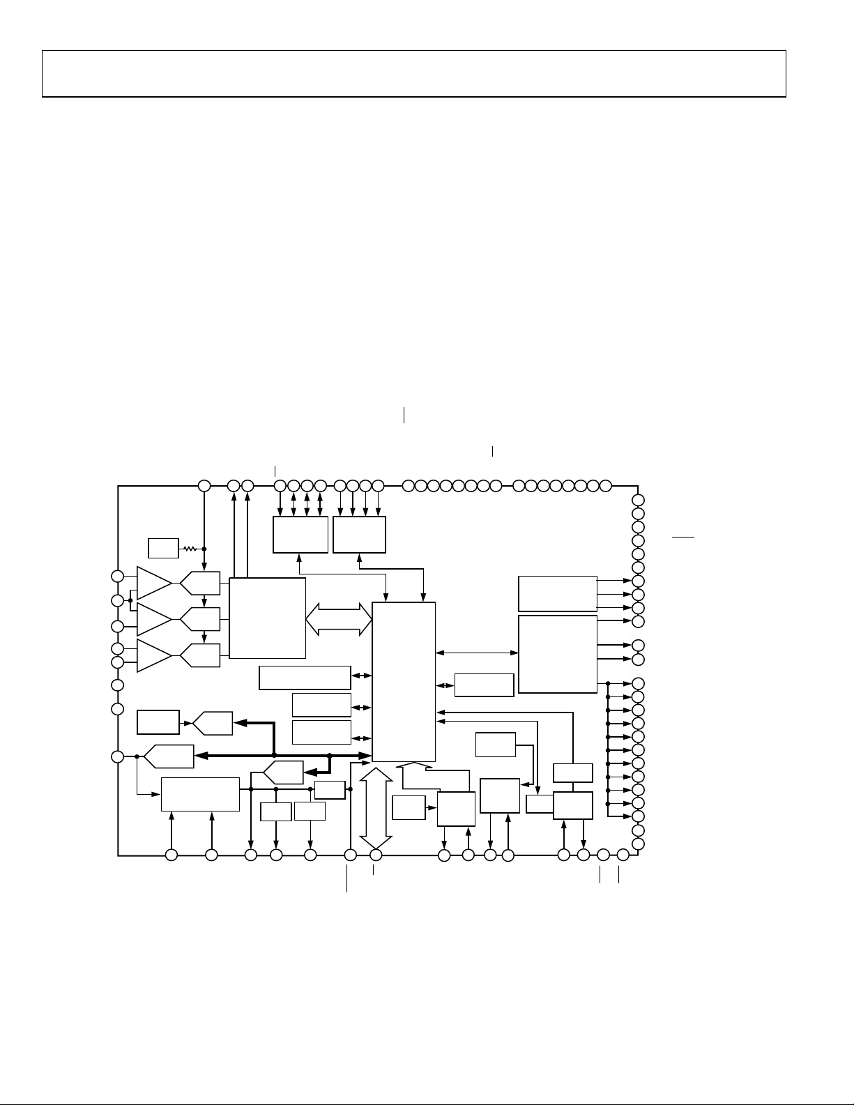
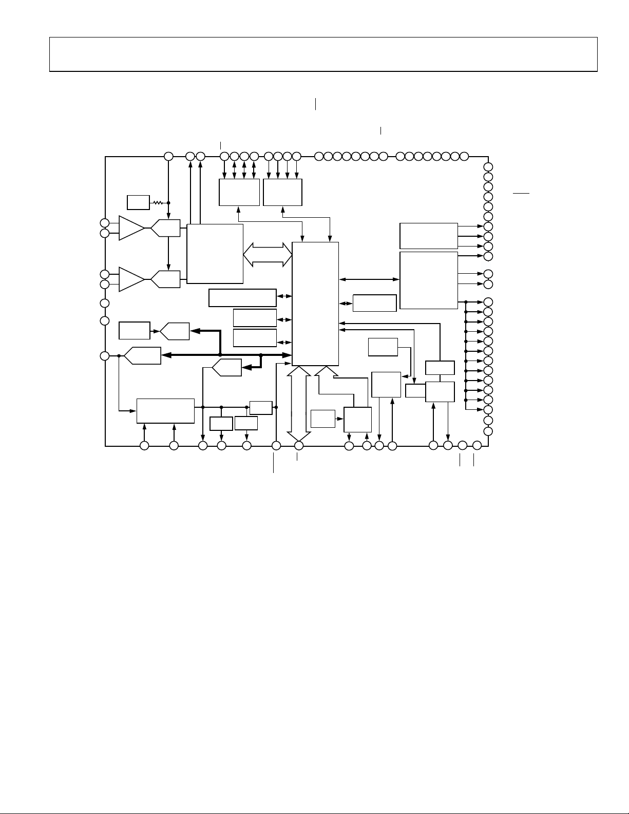
The ADE5166/ADE5169/ADE5566/ADE55691 integrate the
Analog Devices, Inc., energy (ADE) metering IC analog front
end and fixed function DSP solution with an enhanced 8052 MCU
core, a full RTC, an LCD driver, and all the peripherals to make
an electronic energy meter with an LCD display in a single part.
The ADE measurement core includes active, reactive, and apparent
energy calculations, as well as voltage and current rms measurements. This information is accessible for energy billing by using the
built-in energy scalars. Many power line supervisory features such
as SAG, peak, and zero crossing are included in the energy
measurement DSP to simplify energy meter design.
1
Patents pending.
FUNCTIONAL BLOCK DIAGRAMS
The microprocessor functionality includes a single-cycle 8052 core,
a full RTC with a power supply backup pin, an SPI or I
2
C interface,
and two independent UART interfaces. The ready-to-use information from the ADE core reduces the requirement for program
memory size, making it easy to integrate complicated design into
62 kB of flash memory.
The ADE5166/ADE5169 include a 104-segment LCD driver and
the ADE5566/ADE5569 include a 108-segment LCD driver, each
with the capability to store up to four LCD screens in memory. This
driver generates voltages capable of driving LCDs up to 5 V.
TA
4/MOSI/SDA
P0.
TIMER
37
D
x
R
/MISO/ZX
P0.5
UART2
TIMER
UART2
SERIAL
44
2
/SCLK/T0
7/SS/T1/RxD
P0.
P0.6
PORT
2
D
x
T
P1.0/RxD
CHARGE PUMP
104-SEGMENT
LCD DRIVER
RTC
38
2
D
x
R
P24
/TxD
1.2/FP25/ ZX
P1.1
P
P1.3/T2EX/F
3V/5V LCD
2/FP23
P1.4/T
PLL
OSC
4647 48 45
1
L
A
T
X
/FP20
1.5/FP22
P1.6/FP21P1.7
P
12
P2.0/FP18
13
P2.1/FP17
14
P2.2/FP16
44
P2.3 (SDEN/P2.3/TxD2)
LCDVP1
19
LCDVP2
16
LCDVA
18
17
LCDVB
LCDVC
15
4
COM0
.
.
...
.
COM3
1
FP0
35
.
.
...
.
FP15
20
FP16
14
13
FP17
12
FP18
FP19
11
10
FP20
FP21
9
8
FP22
FP23
7
6
FP24
5
FP25
1
FP27
2
FP28
2
1
0
L
T
T
A
N
N
I
I
T
X
07411-201
I
I
DGND
GND
V
BAT
T1/P0.0)
A
K
L
C
S
S
S
SPI/I2C
SERIAL
USER RAM
256 BYTES
USER XRAM
LDO
59
O
S
I
M
2kB
A
T
N
I
V
T
A
D
S
/
I
S
O
M
POR
1
T2T
T0T
3 × 16-BIT
COUNTER
TIMERS
56
T
E
S
E
R
1-PIN
51
X
E
2
SINGLE
CYCLE
EMULATOR
EA
(BCTRL/IN
1/FP19
P0.0
P0.
8052
MCU
DOWNLOADER
DEBUGGER
UART
TIMER
2/CF1
.3/CF2
P0.
P0
ADE5166/ADE5169
WATCHDOG
UART
SERIAL
PORT
36
D
x
T
T
U
O
/
N
I
F
E
R
57
1.20V
REF
+
52
PA
PB
V
V
PGA1
–
53
I
N
+
PGA1
–
55
+
49
P
PGA2
–
50
N
63
54
TEMP
SENSOR
BATTERY
58
ADC
ADC
ADC
TEMP
ADC
ADC
POWER SUPPLY
CONTROL AND
MONIT ORING
64
60
N
I
C
D
V
2
1
F
F
C
C
43 42 39 38 7 6 45 11 43 42 41 40 39 38 37 36 5 6 7 8 9 1038 39 40 41
INTERFACE
ENERGY
MEASUREMENT
DSP
PROGRAM MEMORY
62kB FLASH
VSW
ADC
LDO
61
62
T
D
D
V
D
U
T
N
O
I
W
V
S
V
Figure 1. ADE5166/ADE5169 Functional Block Diagram
Rev. C | Page 4 of 156
ADE5166/ADE5169/ADE5566/ADE5569
A
)
A
K
L
C
S
S
S
SPI/I2C
SERIAL
USER RAM
256 BYTES
USER XRAM
LDO
T
A
D
S
/
I
O
S
S
I
O
1
T2T
T0T
M
M
3 × 16-BIT
COUNTER
TIMERS
2kB
POR
59
56
A
T
T
E
N
I
S
V
E
R
DGND
GND
V
BAT
T
U
O
/
N
I
F
E
R
57
1.20V
REF
+
52
I
P
PGA1
–
53
I
N
+
49
V
P
PGA2
–
50
V
N
63
54
TEMP
SENSOR
58
BATTERY
ADC
POWER SUPPLY
CONTROL AND
MONITORING
64
N
I
C
D
V
ADC
ADC
TEMP
ADC
2
1
F
F
C
C
43 42 39 38 7 6 45 11 43 42 41 40 39 38 37 36 5 6 7 8 9 1038 39 40 41
INTERFACE
ENERGY
MEASUREMENT
DSP
PROGRAM MEMORY
62kB FLASH
VSW
ADC
LDO
616062
T
D
D
V
D
U
T
N
O
I
W
V
S
V
X
E
2
1-PIN
51
EA
SINGLE
CYCLE
8052
MCU
EMULATOR
0
.
0
P
/
1
T
N
I
/
L
R
9
T
1
1
C
F
P
B
F
C
(
/
/
1
2
0
.
.
.
0
0
0
P
P
P
DOWNLOADER
DEBUGGER
UART
TIMER
A
2
T
D
A
x
0
D
X
R
T
Z
S
/
/
/
/
I
1
K
O
T
S
L
2
F
C
/
3
.
0
P
/
S
I
O
S
C
S
S
M
M
/
/
/
/
7
6
5
4
.
.
.
.
0
0
0
0
P
P
P
P
ADE5566/ADE5569
WATCHDOG
TIMER
UART2
TIMER
UART2
SERIAL
PORT
UART
SERIAL
PORT
44
37
36
2
D
D
x
D
x
x
T
R
T
D
x
R
/
0
.
1
P
CHARGE PUMP
108-SEGME NT
LCD DRIVER
RTC
38
2
D
x
R
4
2
P
X
F
Z
/
/
X
5
2
D
E
x
P
2
T
F
T
/
/
/
1
2
3
.
.
.
1
1
1
P
P
P
3V/5V LCD
3
2
P
2
F
2
/
2
P
T
F
/
/
4
5
.
.
1
1
P
P
PLL
OSC
4647 48 45
1
L
A
T
X
1
0
2
2
P
P
F
F
/
/
6
7
.
.
1
1
P
P
12
P2.0/FP18
13
P2.1/FP17
14
P2.2/FP16
44
P2.3 (SDEN/P2.3/TxD2)
19
LCDVP1
LCDVP2
16
LCDVA
18
17
LCDVB
LCDVC
15
4
COM0
.
.
...
.
COM3
1
FP0
35
.
.
...
.
FP15
20
FP16
14
13
FP17
12
FP18
FP19
11
10
FP20
FP21
9
8
FP22
FP23
7
6
FP24
5
FP25
55
FP26
1
FP27
2
FP28
2
1
0
L
T
T
A
N
N
I
I
T
X
07411-001
Figure 2. ADE5566/ADE5569 Functional Block Diagram
Rev. C | Page 5 of 156

ADE5166/ADE5169/ADE5566/ADE5569
SPECIFICATIONS
VDD = 3.3 V ± 5%, AGND = DGND = 0 V, on-chip reference XTALx = 32.768 kHz, T
ENERGY METERING
Table 2.
Parameter Min Typ Max Unit Test Conditions/Comments
MEASUREMENT ACCURACY1
Phase Error Between Channels
PF = 0.8 Capacitive ±0.05 Degrees Phase lead: 37°
PF = 0.5 Inductive ±0.05 Degrees Phase lag: 60°
Active Energy Measurement Error2 0.1 % of reading Over a dynamic range of 1000 to 1 at 25°C
AC Power Supply Rejection2 V
Output Frequency Variation 0.01 % IPx = VP = ±100 mV rms
DC Power Supply Rejection2 V
Output Frequency Variation 0.01 %
Active Energy Measurement Bandwidth1 8 kHz
Reactive Energy Measurement Error2 0.5 % of reading Over a dynamic range of 1000 to 1 at 25°C
V
Measurement Error2 0.5 % of reading Over a dynamic range of 100 to 1 at 25°C
rms
V
Measurement Bandwidth1 3.9 kHz
rms
I
Measurement Error2 0.5 % of reading Over a dynamic range of 500 to 1 at 25°C
rms
I
Measurement Bandwidth1 3.9 kHz
rms
ANALOG INPUTS
Maximum Signal Levels ±500 mV peak VP − VN differential input
ADE5166/ADE5169 ±500 mV peak IPA − IN and IPB − IN differential inputs
ADE5566/ADE5569 ±500 mV peak IP − IN
Input Impedance (DC) 770 kΩ
ADC Offset Error2 ±10 mV PGA1 = PGA2 = 1
±1 mV PGA1 = 16
Gain Error2
Current Channel ±3 % IPA = IPB = 0.5 V dc or IP = 0.5 V dc
Voltage Channel ±3 % VP − VN = 0.5 V dc
Gain Error Match ±0.2 %
CF1 AND CF2 PULSE OUTPUT
Maximum Output Frequency 21.6 kHz
Duty Cycle 50 % If the CF1 or CF2 frequency > 5.55 Hz
Active High Pulse Width 90 ms If the CF1 or CF2 frequency < 5.55 Hz
FAU LT D ETEC T ION3
Fault Detection Threshold
Inactive Input ≠ Active Input 6.25 % of active IPA or IPB active
Input Swap Threshold
Inactive Input > Active Input 6.25 % of active IPA or IPB active
Accuracy Fault Mode Operation
IPA Active, IPB = AGND 0.1 % of reading Over a dynamic range of 500 to 1
IPB Active, IPA = AGND 0.1 % of reading Over a dynamic range of 500 to 1
Fault Detection Delay 3 Seconds
Swap Delay 3 Seconds
1
These specifications are not production tested but are guaranteed by design and/or characterization data on production release.
2
See the Terminology section for definition.
3
Available only in the ADE5166/ADE5169.
MIN
to T
= −40°C to +85°C, unless otherwise noted.
MAX
= 3.3 V + 100 mV rms/120 Hz
DD
= 3.3 V ± 117 mV dc
DD
− VN = 500 mV peak; IPA − IN = 500 mV for
V
P
the ADE5166/ADE5169; I
the ADE5566/ADE5569
− IN = 500 mV for
P
Rev. C | Page 6 of 156

ADE5166/ADE5169/ADE5566/ADE5569
ANALOG PERIPHERALS
Table 3.
Parameter Min Typ Max Unit Test Conditions/Comments
INTERNAL ADCs (BATTERY, TEMPERATURE, V
Power Supply Operating Range 2.4 3.7 V Measured on V
No Missing Codes1 8 Bits
Conversion Delay2 38 μs
ADC Gain
V
Measurement 15.3 mV/LSB
DCIN
V
Measurement 14.6 mV/LSB
BAT
Temperature Measurement 0.83 °C/LSB
ADC Offset
V
Measurement at 3 V 200 LSB
DCIN
V
Measurement at 3.7 V 246 LSB
BAT
Temperature Measurement at 25°C 123 LSB
V
Analog Input
DCIN
Maximum Signal Levels 0 3.3 V
Input Impedance (DC) 1 MΩ
Low V
Detection Threshold 1.09 1.2 1.27 V
DCIN
POWER-ON RESET (POR)
VDD POR
Detection Threshold 2.5 2.95 V
POR Active Timeout Period 33 ms
V
POR
SWOUT
Detection Threshold 1.8 2.2 V
POR Active Timeout Period 20 ms
V
POR
INTD
Detection Threshold 2.0 2.25 V
POR Active Timeout Period 16 ms
V
POR
INTA
Detection Threshold 2.0 2.25 V
POR Active Timeout Period 120 ms
BATTERY SWITCHOVER
Voltage Operating Range (V
VDD to V
Switching
BAT
) 2.4 3.7 V
SWOUT
Switching Threshold (VDD) 2.5 2.95 V
Switching Delay 10 ns When VDD to V
30 ms When VDD to V
V
to VDD Switching
BAT
Switching Threshold (VDD) 2.5 2.95 V
Switching Delay 30 ms Based on VDD > 2.75 V
V
to V
SWOUT
Leakage Current 10 nA V
BAT
LCD, CHARGE PUMP ACTIVE
Charge Pump Capacitance Between
LCDVP1 and LCDVP2
LCDVA, LCDVB, LCDVC Decoupling Capacitance 470 nF
LCDVA 0 1.9 V
LCDVB 0 3.8 V 1/3 bias mode
LCDVC 0 5.8 V 1/3 bias mode
V1 Segment Line Voltage LCDVA − 0.1 LCDVA V Current on segment line = −2 μA
V2 Segment Line Voltage LCDVB − 0.1
V3 Segment Line Voltage LCDVC − 0.1
DC Voltage Across Segment and COMx Pin 50 mV
)
DCIN
100 nF
Rev. C | Page 7 of 156
LCDVB V Current on segment line = −2 μA
LCDVC V Current on segment line = −2 μA
SWOUT
switch is activated by VDD
BAT
switch is activated by V
BAT
= 0 V, V
BAT
= 3.43 V, TA = 25°C
SWOUT
LCDVC − LCDVB, LCDVC − LCDVA, or
LCDVB − LCDVA
DCIN

ADE5166/ADE5169/ADE5566/ADE5569
Parameter Min Typ Max Unit Test Conditions/Comments
LCD, RESISTOR LADDER ACTIVE
Leakage Current ±20 nA 1/2 and 1/3 bias modes, no load
V1 Segment Line Voltage LCDVA − 0.1 LCDVA V Current on segment line = −2 μA
V2 Segment Line Voltage LCDVB − 0.1 LCDVB V Current on segment line = −2 μA
V3 Segment Line Voltage LCDVC − 0.1 LCDVC V Current on segment line = −2 μA
ON-CHIP REFERENCE Nominal 1.2035 V
Reference Error −2.2 +2.2 mV TA = 25°C, f
Power Supply Rejection 80 dB
Temperature Coefficient1 10 50 ppm/°C f
1
These specifications are not production tested but are guaranteed by design and/or characterization data on production release.
2
Delay between ADC conversion request and interrupt set.
= 1.024 MHz
CORE
DIGITAL INTERFACE
Table 4.
Parameter Min Typ Max Unit Test Conditions/Comments
LOGIC INPUTS1
All Inputs Except XTAL1, XTAL2, BCTRL,
, INT1, RESET
INT0
Input High Voltage, V
Input Low Voltage, V
2.0 V
INH
0.8 V
INL
BCTRL, INT0, INT1, RESET
Input High Voltage, V
Input Low Voltage, V
1.3 V
INH
0.8 V
INL
Input Currents
RESET
Port 0, Port 1, Port 2 ±100 nA
−3.75 −8.5 μA
Input Capacitance 10 pF All digital inputs
FLASH MEMORY
Endurance2 20,000 Cycles At 25°C
Data Retention3 20 Years TJ = 85°C
CRYSTAL OSCILLATOR4
Crystal Equivalent Series Resistance 30 50 kΩ
Crystal Frequency 32 32.768 33.5 kHz
XTAL1 Input Capacitance 12 pF
XTAL2 Output Capacitance 12 pF
MCU CLOCK RATE (f
) 4.096 MHz Crystal = 32.768 kHz and CD bits = 0b000
CORE
32 kHz Crystal = 32.768 kHz and CD bits = 0b111
LOGIC OUTPUTS
Output High Voltage, VOH 2.4 V VDD = 3.3 V ± 5%
I
80 μA
SOURCE
Output Low Voltage, V
I
2 mA
SINK
5
0.4 V VDD = 3.3 V ± 5%
OL
START-UP TIME6
PSM0 Power-On Time 880 ms VDD at 2.75 V to PSM0 code execution
From Power Saving Mode 1 (PSM1)
PSM1 to PSM0 130 ms VDD at 2.75 V to PSM0 code execution
From Power Saving Mode 2 (PSM2)
PSM2 to PSM1 48 ms Wake-up event to PSM1 code execution
PSM2 to PSM0 186 ms VDD at 2.75 V to PSM0 code execution
100 nA
RESET = V
Internal pull-up disabled, input = 0 V or
V
SWOUT
Internal pull-up enabled, input = 0 V,
= 3.3 V
V
SWOUT
= 1.024 MHz
CORE
= 3.3 V
SWOUT
Rev. C | Page 8 of 156

ADE5166/ADE5169/ADE5566/ADE5569
Parameter Min Typ Max Unit Test Conditions/Comments
POWER SUPPLY INPUTS
VDD 3.13 3.3 3.46 V
V
2.4 3.3 3.7 V
BAT
INTERNAL POWER SUPPLY SWITCH (V
V
to V
BAT
VDD to V
V
to/from VDD Switching Open Time 40 ns
BAT
On Resistance 12 Ω V
SWOUT
On Resistance 9 Ω VDD = 3.13 V
SWOUT
BCTRL State Change and Switch Delay 18 μs
V
Output Current Drive 6 mA
SWOUT
POWER SUPPLY OUTPUTS
V
2.3 2.70 V
INTA
V
2.3 2.70 V
INTD
V
Power Supply Rejection 60 dB
INTA
V
Power Supply Rejection 50 dB
INTD
POWER SUPPLY CURRENTS
Current in Normal Mode (PSM0) 4.4 5.3 mA f
2.2 mA f
1.6 mA f
3 3.9 mA
Current in Battery Mode (PSM1) 3.3 5.05 mA f
1 mA f
Current in Sleep Mode (PSM2) 38 μA
1.7 μA RTC only, TA = 25°C, V
1
Specifications guaranteed by design.
2
Endurance is qualified as per JEDEC Standard 22 Method A117 and measured at −40°C, +25°C, +85°C, and +125°C.
3
Retention lifetime equivalent at junction temperature (TJ) = 85°C as per JEDEC Standard 22 Method A117. Retention lifetime derates with junction temperature.
4
Recommended crystal specifications.
5
Test carried out with all the I/Os set to a low output level.
6
Delay between power supply valid and execution of first instruction by 8052 core.
)
SWOUT
= 2.4 V
BAT
= 4.096 MHz, LCD and meter active
CORE
= 1.024 MHz, LCD and meter active
CORE
= 32.768 kHz, LCD and meter active
CORE
= 4.096 MHz; metering ADC and DSP,
f
CORE
powered down
= 4.096 MHz, LCD active, V
CORE
= 1.024 MHz, LCD active
CORE
= 3.7 V
BAT
LCD active with charge pump at 3.3 V + RTC,
= 3.3 V
V
BAT
= 3.3 V
BAT
Rev. C | Page 9 of 156
ADE5166/ADE5169/ADE5566/ADE5569
V
–
V
TIMING SPECIFICATIONS
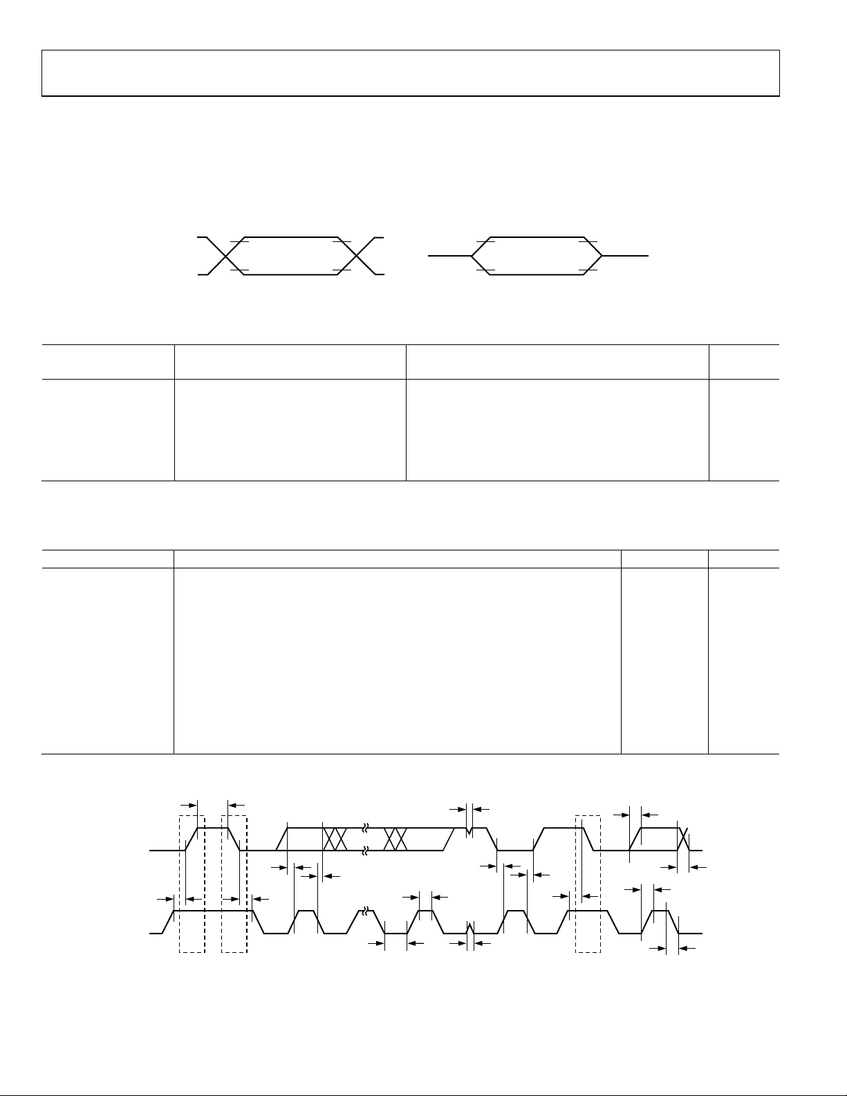
AC inputs during testing were driven at V
and at 0.45 V for Logic 0. Timing measurements were made at V
minimum for Logic 1 and at V
maximum for Logic 0, as shown in
IL
Figure 3.
0.5
SWOUT
0.45V
Table 5. Clock Input (External Clock Driven XTAL1) Parameters
32.768 kHz External Crystal
Parameter Description Min Typ Max Unit
tCK XTAL1 period 30.52 μs
t
XTAL1 width low 6.26 μs
CKL
t
XTAL1 width high 6.26 μs
CKH
t
XTAL1 rise time 9 ns
CKR
t
XTAL1 fall time 9 ns
CKF
1/t
Core clock frequency1 1.024 MHz
CORE
1
The ADE5166/ADE5169/ADE5566/ADE5569 internal PLL locks onto a multiple (512×) of the 32.768 kHz external crystal frequency to provide a stable 4.096 MHz internal
clock for the system. The core can operate at this frequency or at a binary submultiple defined by the CD bits of the POWCON SFR, Address 0xC5[2:0] (see Tabl e 26).
− 0.5 V for Logic 1
SWOUT
0.2V
0.2V
+ 0.9V
SWOUT
TEST POINTS
– 0.1V
SWOUT
Figure 3. Timing Waveform Characteristics
IH
For timing purposes, a port pin is no longer floating when
a 100 mV change from load voltage occurs. A port pin begins
to float when a 100 mV change from the loaded V
occurs, as shown in Figure 3.
C
= 80 pF for all outputs, unless otherwise noted. VDD = 2.7 V
LOAD
to 3.6 V; all specifications T
V
– 0.1V
LOAD
V
LOAD
V
+ 0.1V
LOAD
TIMING
REFERENCE
POINTS
MIN
to T
V
LOAD
V
LOAD
, unless otherwise noted.
MAX
– 0.1V
V
LOAD
– 0.1V
07411-002
OH/VOL
level
Table 6. I2C-Compatible Interface Timing Parameters (400 kHz)
Parameter Description Typ Unit
t
Bus-free time between stop condition and start condition 1.3 μs
BUF
tL SCLK low pulse width 1.36 μs
tH SCLK high pulse width 1.14 μs
t
Start condition hold time 251.35 μs
SHD
t
Data setup time 740 ns
DSU
t
Data hold time 400 ns
DHD
t
Setup time for repeated start 12.5 ns
RSU
t
Stop condition setup time 400 ns
PSU
tR Rise time of both SCLK and SDATA 200 ns
tF Fall time of both SCLK and SDATA 300 ns
1
t
Pulse width of spike suppressed 50 ns
SUP
1
Input filtering on both the SCLK and SDATA suppresses noise spikes of <50 ns.
t
SDATA (I/O)
t
SCLK (I)
PSU
PS
STOP
CONDITI ON
BUF
START
CONDITI ON
MSB
t
DSU
t
SHD
1
t
DHD
Figure 4. I
2TO 7
2
C-Compatible Interface Timing
t
SUP
LSB ACK MSB
t
DSU
t
H
89 1
t
t
SUP
L
t
DHD
t
RSU
S(R)
REPEATED
START
t
R
t
F
t
t
F
R
07411-003
Rev. C | Page 10 of 156
ADE5166/ADE5169/ADE5566/ADE5569
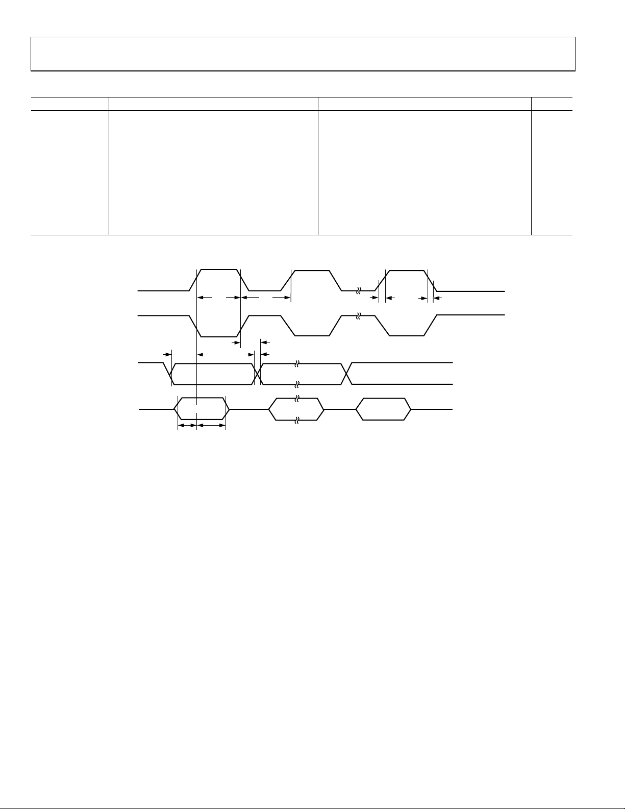
Table 7. SPI Master Mode Timing Parameters (SPICPHA = 1)
Parameter Description Min Typ Max Unit
tSL SCLK low pulse width 2
tSH SCLK high pulse width 2
t
Data output valid after SCLK edge 3 × t
DAV
t
Data input setup time before SCLK edge 0 ns
DSU
t
Data input hold time after SCLK edge t
DHD
tDF Data output fall time 19 ns
tDR Data output rise time 19 ns
tSR SCLK rise time 19 ns
tSF SCLK fall time 19 ns
1
t
depends on the clock divider or the CD bits of the POWCON SFR, Address 0xC5[2:0] (see Table 26); t
CORE
SCLK
(SPICPOL = 0)
SCLK
(SPICPOL = 1)
MOSI
t
SH
t
DAV
t
SL
MSB
t
DF
SPIR
SPIR
CORE
t
DR
BITS[6:1]
1
× t
ns
CORE
1
× t
ns
CORE
1
ns
= 2CD/4.096 MHz.
CORE
t
SR
t
SF
LSB
1
ns
CORE
MISO
MSB IN
t
t
DSU
DHD
BITS[ 6:1]
LSB IN
07411-004
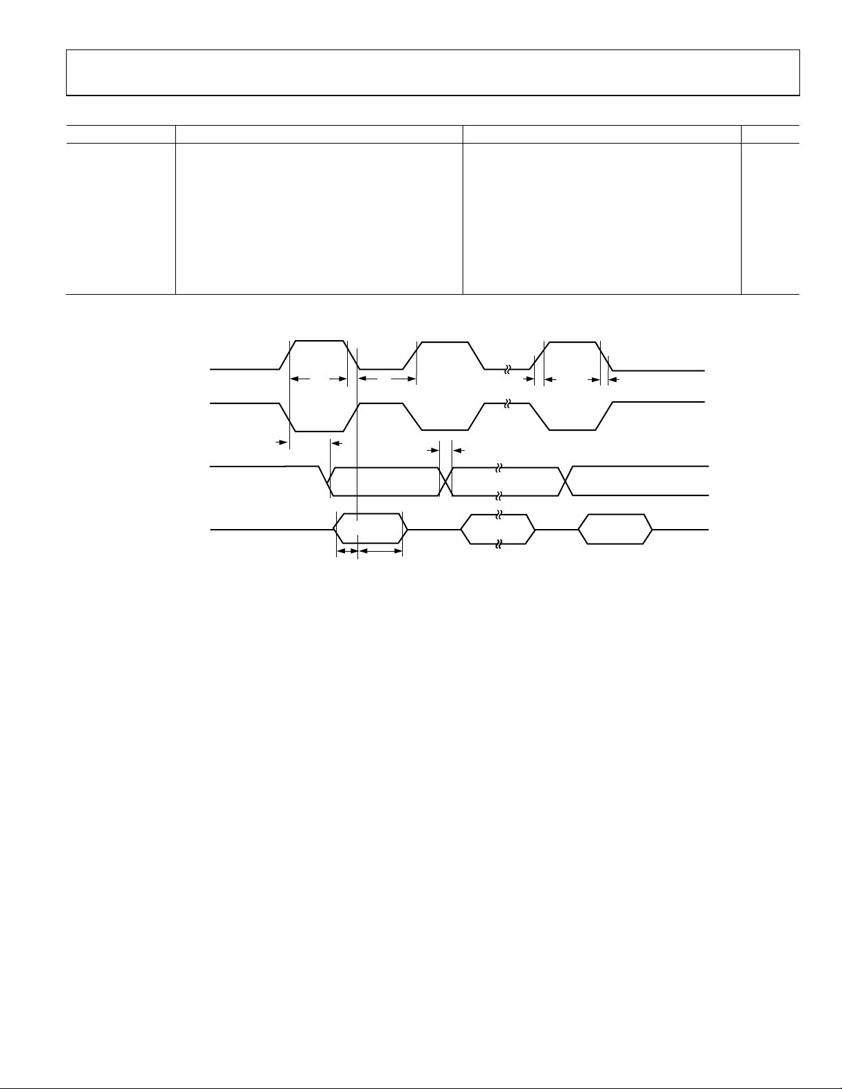
Figure 5. SPI Master Mode Timing (SPICPHA = 1)
Rev. C | Page 11 of 156
ADE5166/ADE5169/ADE5566/ADE5569
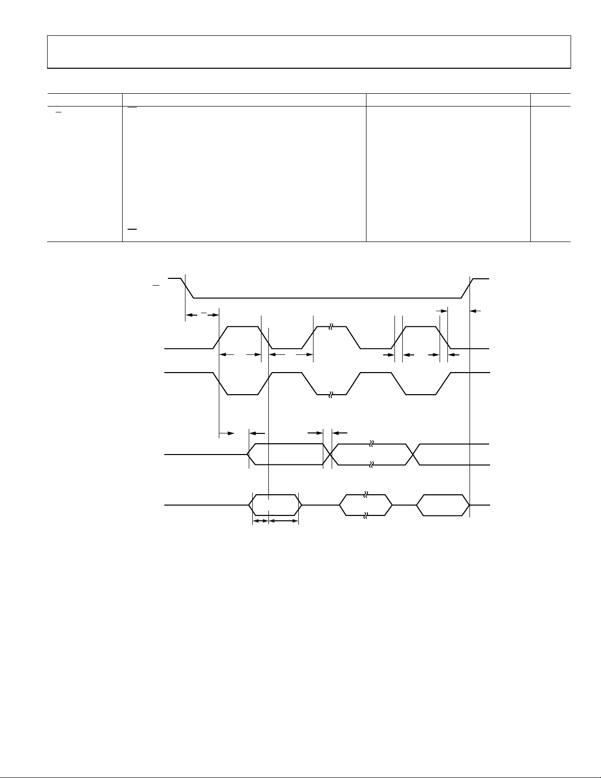
Table 8. SPI Master Mode Timing Parameters (SPICPHA = 0)
Parameter Description Min Typ Max Unit
tSL SCLK low pulse width 2
tSH SCLK high pulse width 2
t
Data output valid after SCLK edge 3 × t
DAV
t
Data output setup before SCLK edge 75 ns
DOSU
t
Data input setup time before SCLK edge 0 ns
DSU
t
Data input hold time after SCLK edge t
DHD
tDF Data output fall time 19 ns
tDR Data output rise time 19 ns
tSR SCLK rise time 19 ns
tSF SCLK fall time 19 ns
1
t
depends on the clock divider or the CD bits of the POWCON SFR, Address 0xC5[2:0] (see Table 26); t
CORE
SCLK
(SPICPOL = 0)
SCLK
(SPICPOL = 1)
MOSI
t
DOSU
MSB
t
SH
t
SL
t
DAV
t
DF
t
DR
BITS[6:1]
SPIR
SPIR
CORE
1
× t
(SPIR + 1) × t
CORE
1
× t
(SPIR + 1) × t
CORE
1
ns
= 2CD/4.096 MHz.
CORE
t
SR
LSB
t
SF
1
ns
CORE
1
ns
CORE
1
ns
CORE
MISO
t
DSU
MSB IN
t
BITS[6:1]
DHD
LSB IN
07411-005
Figure 6. SPI Master Mode Timing (SPICPHA = 0)
Rev. C | Page 12 of 156
ADE5166/ADE5169/ADE5566/ADE5569
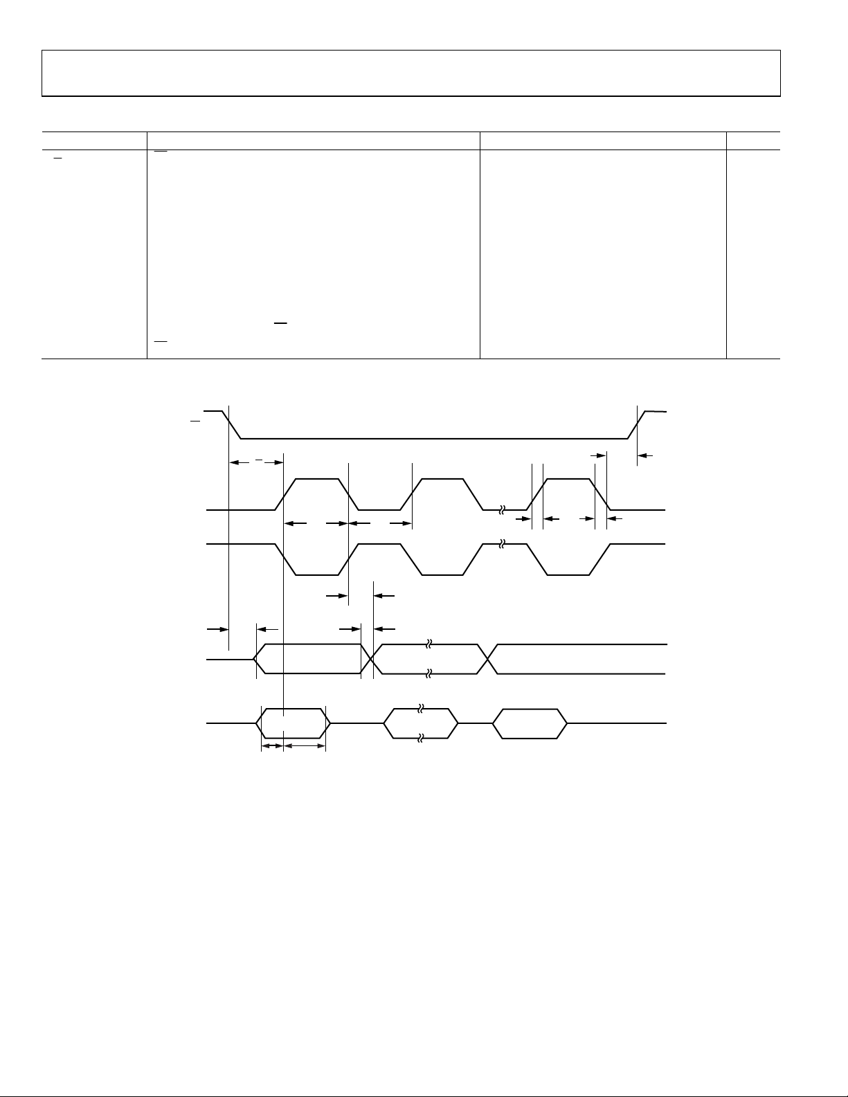
Table 9. SPI Slave Mode Timing Parameters (SPICPHA = 1)
Parameter Description Min Typ Max Unit
tSS
to SCLK edge
SS
tSL SCLK low pulse width 6 × t
tSH SCLK high pulse width 6 × t
t
Data output valid after SCLK edge 25 ns
DAV
t
Data input setup time before SCLK edge 0 ns
DSU
t
Data input hold time after SCLK edge 2 × t
DHD
tDF Data output fall time 19 ns
tDR Data output rise time 19 ns
tSR SCLK rise time 19 ns
tSF SCLK fall time 19 ns
t
SFS
1
t
depends on the clock divider or the CD bits of the POWCON SFR, Address 0xC5[2:0] (see Table 26); t
CORE
high after SCLK edge
SS
SS
t
SS
145 ns
1
ns
CORE
1
ns
CORE
1
+ 0.5 μs
CORE
0 ns
= 2CD/4.096 MHz.
CORE
t
SFS
SCLK
(SPICPOL = 0)
SCLK
(SPICPOL = 1)
MISO
MOSI
t
t
SH
DAV
t
DSU
MSB IN
MSB
t
DHD
t
SL
t
SR
t
DF
t
DR
BITS[6:1]
BITS[6:1]
t
SF
LSB
LSB IN
07411-006
Figure 7. SPI Slave Mode Timing (SPICPHA = 1)
Rev. C | Page 13 of 156
ADE5166/ADE5169/ADE5566/ADE5569
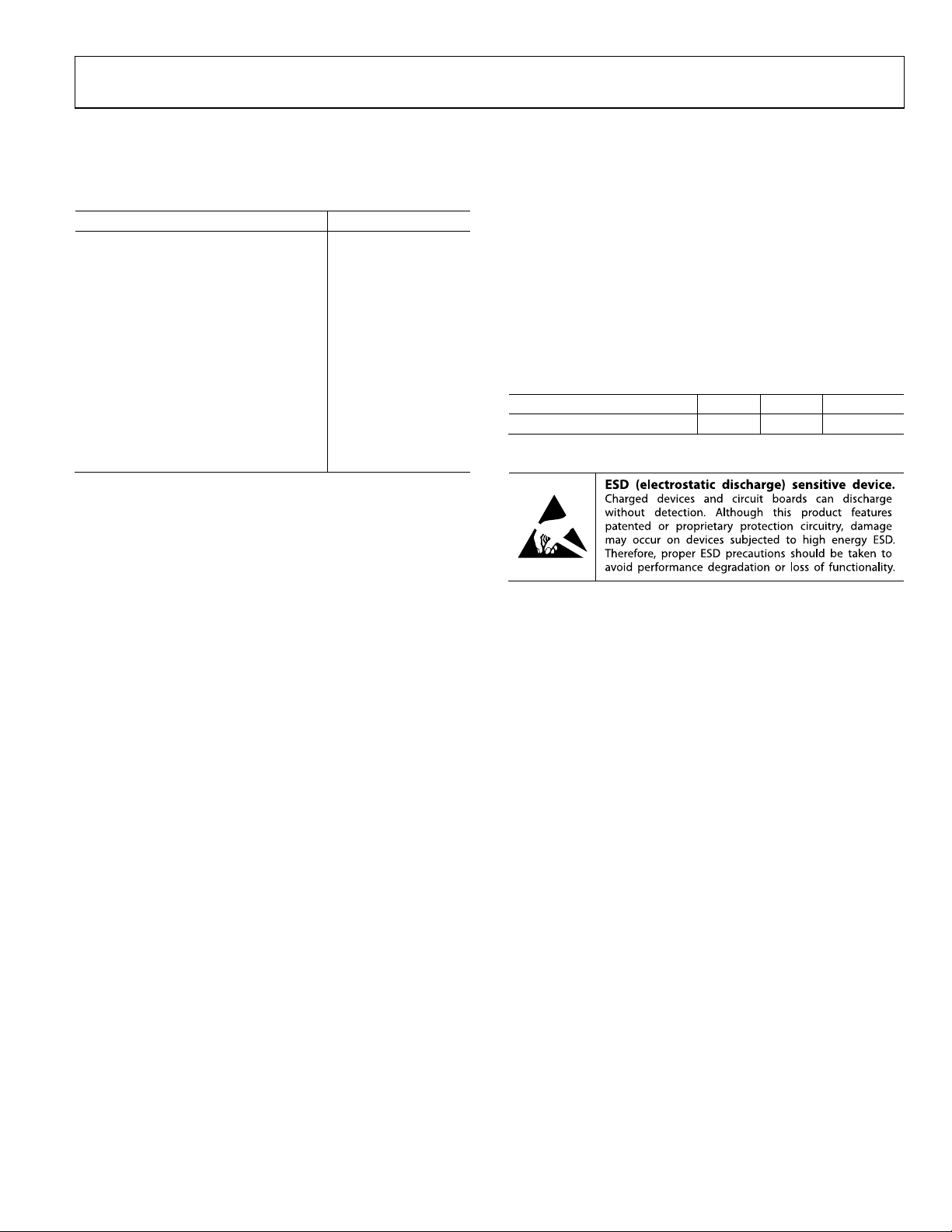
Table 10. SPI Slave Mode Timing Parameters (SPICPHA = 0)
Parameter Description Min Typ Max Unit
tSS
to SCLK edge
SS
tSL SCLK low pulse width 6 × t
tSH SCLK high pulse width 6 × t
t
Data output valid after SCLK edge 25 ns
DAV
t
Data input setup time before SCLK edge 0 ns
DSU
t
Data input hold time after SCLK edge 2 × t
DHD
tDF Data output fall time 19 ns
tDR Data output rise time 19 ns
tSR SCLK rise time 19 ns
tSF SCLK fall time 19 ns
t
DOSS
t
SFS
1
t
depends on the clock divider or the CD bits of the POWCON SFR, Address 0xC5[2:0] (see Table 26); t
CORE
Data output valid after SS
high after SCLK edge
SS
edge
SS
t
SS
145 ns
1
ns
CORE
1
ns
CORE
1
+ 0.5 μs
CORE
0 ns
0 ns
= 2CD/4.096 MHz.
CORE
t
SFS
SCLK
(SPICPOL = 0)
SCLK
(SPICPOL = 1)
MISO
MOSI
t
DOSS
t
DSU
MSB IN
MSB
t
DHD
t
SH
t
DF
t
SL
t
DAV
t
DR
BITS[6:1]
BITS[6:1]
t
LSB IN
LSB
t
SF
07411-007
SR
Figure 8. SPI Slave Mode Timing (SPICPHA = 0)
Rev. C | Page 14 of 156
ADE5166/ADE5169/ADE5566/ADE5569
ABSOLUTE MAXIMUM RATINGS
TA = 25°C, unless otherwise noted.
Table 11.
Parameter Rating
VDD to DGND −0.3 V to +3.7 V
V
to DGND −0.3 V to +3.7 V
BAT
V
to DGND −0.3 V to V
DCIN
Input LCD Voltage to AGND, LCDVA,
LCDVB, LCDVC
1
Analog Input Voltage to AGND, VP, VN,
, IPB, and IN
I
P/IPA
−0.3 V to V
−2 V to +2 V
Digital Input Voltage to DGND −0.3 V to V
Digital Output Voltage to DGND −0.3 V to V
SWOUT
SWOUT
SWOUT
SWOUT
+ 0.3 V
+ 0.3 V
+ 0.3 V
+ 0.3 V
Operating Temperature Range (Industrial) −40°C to +85°C
Storage Temperature Range −65°C to +150°C
64-Lead LQFP, Power Dissipation
Lead Temperature (Soldering, 30 sec) 300°C
1
When used with external resistor divider.
Stresses above those listed under Absolute Maximum Ratings
may cause permanent damage to the device. This is a stress
rating only; functional operation of the device at these or any
other conditions above those indicated in the operational
section of this specification is not implied. Exposure to absolute
maximum rating conditions for extended periods may affect
device reliability.
THERMAL RESISTANCE
θJA is specified for the worst-case condition, that is, a device
soldered in a circuit board for surface-mount packages.
Table 12. Thermal Resistance
Package Type θJA θ
Unit
JC
64-Lead LQFP 60 20.5 °C/W
ESD CAUTION
Rev. C | Page 15 of 156
ADE5166/ADE5169/ADE5566/ADE5569
T
PIN CONFIGURATIONS AND FUNCTION DESCRIPTIONS
INTA
BAT
V
V
59
58
57
TOP VIEW
(Not to Scale)
24
IN/OU
PB
REF
I
AGND53I
RESET
56
55
54
25
26
FP927FP828FP729FP630FP531FP432FP3
FP11
FP10
N
51EA50
P
V
V
49
48
INT0
47
XTAL1
46
XTAL2
45
BCTRL/INT1/P0.0
44
SDEN/P2.3/TxD2
43
P0.2/CF1
42
P0.3/CF2
41
P0.4/MOSI/SDATA
40
P0.5/MISO/ZX
39
P0.6/SCLK/T0
38
P0.7/SS/T1/RxD2
37
P1.0/RxD
36
P1.1/TxD
35
FP0
34
FP1
33
FP2
07411-010
N
PA
I
52
COM3/F P27
COM2/F P28
COM1
COM0
P1.2/FP25/ZX
P1.3/T2EX/FP24
P1.4/T2/ FP23
P1.5/FP22
P1.6/FP21
P1.7/FP20
P0.1/FP19
P2.0/FP18
P2.1/FP17
P2.2/FP16
LCDVC
LCDVP2
DCIN
INTD
SWOUT
V
DGND62V
64
63
1
PIN 1
2
3
4
5
6
7
8
9
10
11
12
13
14
15
16
17
18
LCDVA
LCDVB
DD
V
V
61
60
ADE5166/ADE5169
19
20
FP1521FP1422FP1323FP12
LCDVP1
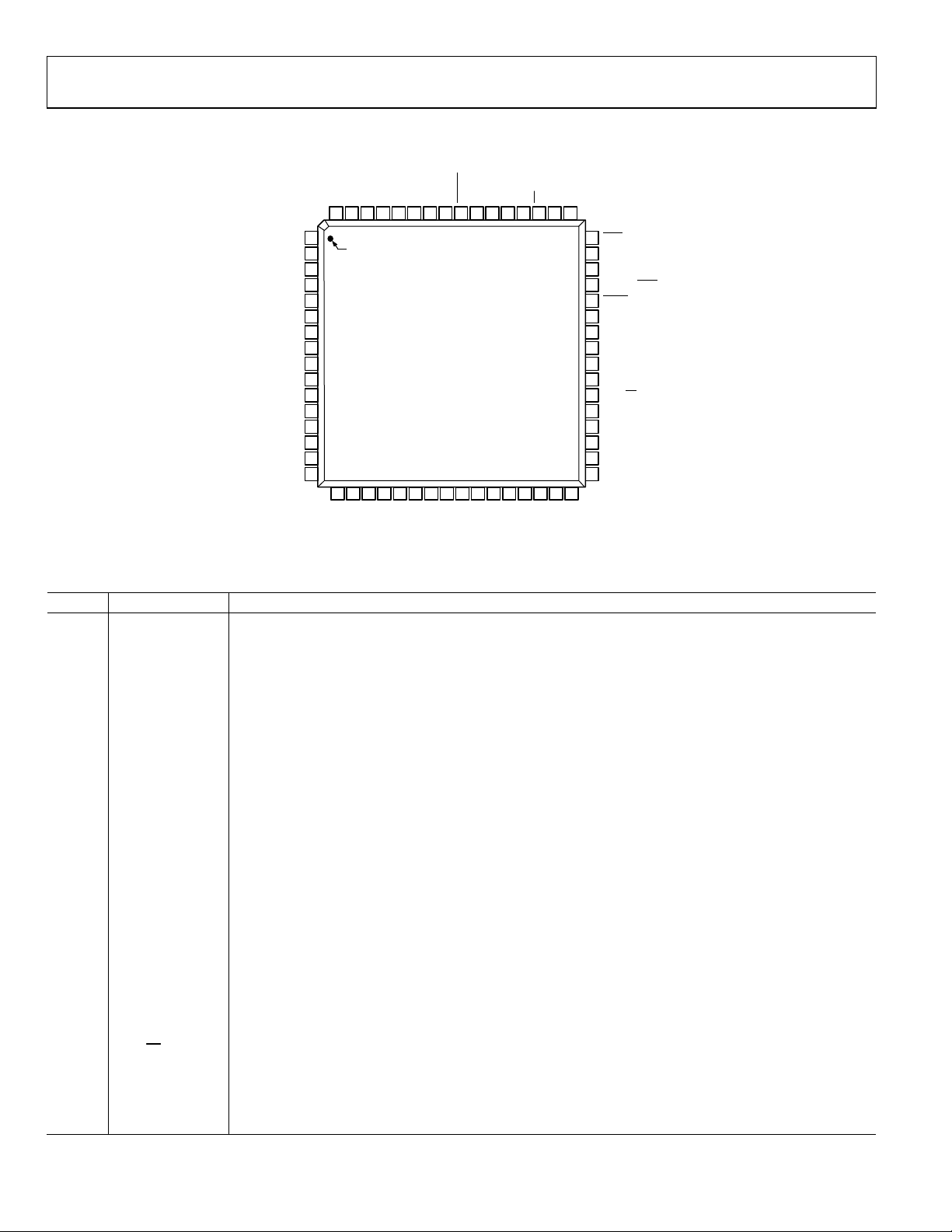
Figure 9. ADE5166/ADE5169 Pin Configuration
Table 13. Pin Function Descriptions
Pin No. Mnemonic Description
1 COM3/FP27 Common Output 3/LCD Segment Output 27. COM3 is used for the LCD backplane.
2 COM2/FP28 Common Output 2/LCD Segment Output 28. COM2 is used for the LCD backplane.
3 COM1 Common Output 1. COM1 is used for the LCD backplane.
4 COM0 Common Output 0. COM0 is used for the LCD backplane.
5 P1.2/FP25/ZX General-Purpose Digital I/O Port 1.2/LCD Segment Output 25/ZX Output.
6 P1.3/T2EX/FP24 General-Purpose Digital I/O Port 1.3/Timer 2 Control Input/LCD Segment Output 24.
7 P1.4/T2/FP23 General-Purpose Digital I/O Port 1.4/Timer 2 Input/LCD Segment Output 23.
8 P1.5/FP22 General-Purpose Digital I/O Port 1.5/LCD Segment Output 22.
9 P1.6/FP21 General-Purpose Digital I/O Port 1.6/LCD Segment Output 21.
10 P1.7/FP20 General-Purpose Digital I/O Port 1.7/LCD Segment Output 20.
11 P0.1/FP19 General-Purpose Digital I/O Port 0.1/LCD Segment Output 19.
12 P2.0/FP18 General-Purpose Digital I/O Port 2.0/LCD Segment Output 18.
13 P2.1/FP17 General-Purpose Digital I/O Port 2.1/LCD Segment Output 17.
14 P2.2/FP16 General-Purpose Digital I/O Port 2.2/LCD Segment Output 16.
15 LCDVC Output Port for LCD Levels. This pin should be decoupled with a 470 nF capacitor.
16 LCDVP2
Analog Output. A 100 nF capacitor should be connected between this pin and LCDVP1 for the internal LCD
charge pump device.
17, 18 LCDVB, LCDVA Output Ports for LCD Levels. These pins should be decoupled with a 470 nF capacitor.
19 LCDVP1
Analog Output. A 100 nF capacitor should be connected between this pin and LCDVP2 for the internal LCD
charge pump device.
20 to 35 FP15 to FP0 LCD Segment Output 15 to LCD Segment Output 0.
36 P1.1/TxD General-Purpose Digital I/O Port 1.1/Transmitter Data Output (Asynchronous).
37 P1.0/RxD General-Purpose Digital I/O Port 1.0/Receive Data Input (Asynchronous).
38
/T1/RxD2 General-Purpose Digital I/O Port 0.7/Slave Select When SPI Is in Slave Mode/Timer 1 Input/Receive Data
P0.7/SS
Input 2 (Asynchronous).
39 P0.6/SCLK/T0 General-Purpose Digital I/O Port 0.6/Clock Output for I2C or SPI Port/Timer 0 Input.
40 P0.5/MISO/ZX General-Purpose Digital I/O Port 0.5/Data Input for SPI Port/ZX Output.
41 P0.4/MOSI/SDATA General-Purpose Digital I/O Port 0.4/Data Output for SPI Port/I2C-Compatible Data Line.
Rev. C | Page 16 of 156
ADE5166/ADE5169/ADE5566/ADE5569
Pin No. Mnemonic Description
42 P0.3/CF2
43 P0.2/CF1
44
45
/P2.3/TxD2 Serial Download Mode Enable/General-Purpose Digital Output Port 2.3/Transmitter Data Output 2
SDEN
BCTRL/INT1
/P0.0 Digital Input for Battery Control/External Interrupt Input 1/General-Purpose Digital I/O Port 0.0. This logic
46 XTAL2
47 XTAL1
48
INT0
49, 50 VP, VN
51
Input for Emulation. When held high, this input enables the device to fetch code from internal program
EA
52, 53 IPA, IN
54 AGND Ground Reference for Analog Circuitry.
55 IPB
56
57 REF
58 V
59 V
RESET
IN/OUT
BAT
INTA
60 VDD
61 V
62 V
SWOUT
INTD
63 DGND Ground Reference for Digital Circuitry.
64 V
DCIN
General-Purpose Digital I/O Port 0.3/Calibration Frequency Logic Output 2. The CF2 logic output gives
instantaneous active, reactive, or apparent power or I
information.
rms
General-Purpose Digital I/O Port 0.2/Calibration Frequency Logic Output 1. The CF1 logic output gives
instantaneous active, reactive, or apparent power or I
information.
rms
(Asynchronous). This pin is used to enable serial download mode through a resistor when pulled low on
power-up or reset. On reset, this pin momentarily becomes an input, and the status of the pin is sampled.
If there is no pull-down resistor in place, the pin momentarily goes high, and then user code is executed.
If the pin is pulled down on reset, the embedded serial download/debug kernel executes, and this pin remains
low during the internal program execution. After reset, this pin can be used as a digital output port pin (P2.3)
or as Transmitter Data Output 2 (asynchronous).
or V
input connects V
DD
BAT
to V
open, the connection between V
internally when set to logic high or logic low, respectively. When left
SWOUT
or V
BAT
and V
DD
is selected internally.
SWOUT
A crystal can be connected across this pin and XTAL1 (see the XTAL1 pin description) to provide a clock
source. The XTAL2 pin can drive one CMOS load when an external clock is supplied at XTAL1 or by the gate
oscillator circuit. An internal 6 pF capacitor is connected to this pin.
An external clock can be provided at this logic input. Alternatively, a tuning fork crystal can be connected
across XTAL1 and XTAL2 to provide a clock source. The clock frequency for specified operation is 32.768 kHz.
An internal 6 pF capacitor is connected to this pin.
External Interrupt Input 0.
Analog Inputs for Voltage Channel. These inputs are fully differential voltage inputs with a maximum
differential level of ±500 mV for specified operation. This channel also has an internal PGA.
memory locations. The ADE5166/ADE5169 do not support external code memory. This pin should not be left
floating.
Analog Inputs for Current Channel. These inputs are fully differential voltage inputs with a maximum
differential level of ±500 mV for specified operation. This channel also has an internal PGA.
Analog Input for Second Current Channel. This input is fully differential with a maximum differential level of
±500 mV, referred to I
for specified operation. This channel also has an internal PGA.
N
Reset Input, Active Low.
Access to On-Chip Voltage Reference. The on-chip reference has a nominal value of 1.2 V ± 0.1% and a typical
temperature coefficient of 50 ppm/°C maximum. This pin should be decoupled with a 1 μF capacitor in
parallel with a ceramic 100 nF capacitor.
Power Supply Input from the Battery with a 2.4 V to 3.7 V Range. This pin is connected internally to V
when
DD
the battery is selected as the power supply.
Access to On-Chip 2.5 V Analog LDO. No external active circuitry should be connected to this pin. This pin
should be decoupled with a 10 μF capacitor in parallel with a ceramic 100 nF capacitor.
3.3 V Power Supply Input from the Regulator. This pin is connected internally to V
when the regulator is
SWOUT
selected as the power supply. This pin should be decoupled with a 10 μF capacitor in parallel with a ceramic
100 nF capacitor.
3.3 V Power Supply Output. This pin provides the supply voltage for the LDOs and the internal circuitry. This
pin should be decoupled with a 10 μF capacitor in parallel with a ceramic 100 nF capacitor.
Access to On-Chip 2.5 V Digital LDO. No external active circuitry should be connected to this pin. This pin
should be decoupled with a 10 μF capacitor in parallel with a ceramic 100 nF capacitor.
Analog Input for DC Voltage Monitoring. The maximum input voltage on this pin is V
with respect to
SWOUT
AGND. This pin is used to monitor the preregulated dc voltage.
Rev. C | Page 17 of 156
ADE5166/ADE5169/ADE5566/ADE5569
T
INTA
BAT
V
V
59
58
57
TOP VIEW
(Not to Scale)
24
IN/OU
FP26
REF
AGND53I
RESET
56 55
54
25
26
FP927FP828FP729FP630FP531FP432FP3
FP11
FP10
N
P
I
52 51EA50
N
P
V
V
49
48
INT0
47
XTAL1
46
XTAL2
45
BCTRL/INT1/P0.0
44
SDEN/P2.3/TxD2
43
P0.2/CF1
42
P0.3/CF2
41
P0.4/MOSI/SDATA
40
P0.5/MISO/ZX
39
P0.6/SCLK/T0
38
P0.7/SS/T1/RxD2
37
P1.0/RxD
36
P1.1/TxD
35
FP0
34
FP1
33
FP2
07411-028
COM3/F P27
COM2/F P28
COM1
COM0
P1.2/FP25/ZX
P1.3/T2EX/FP24
P1.4/T2/ FP23
P1.5/FP22
P1.6/FP21
P1.7/FP20
P0.1/FP19
P2.0/FP18
P2.1/FP17
P2.2/FP16
LCDVC
LCDVP2
DCIN
INTD
SWOUT
V
DGND62V
64
63
1
PIN 1
2
3
4
5
6
7
8
9
10
11
12
13
14
15
16
17
18
LCDVA
LCDVB
DD
V
V
61
60
ADE5566/ADE5569
19
20
FP1521FP1422FP1323FP12
LCDVP1
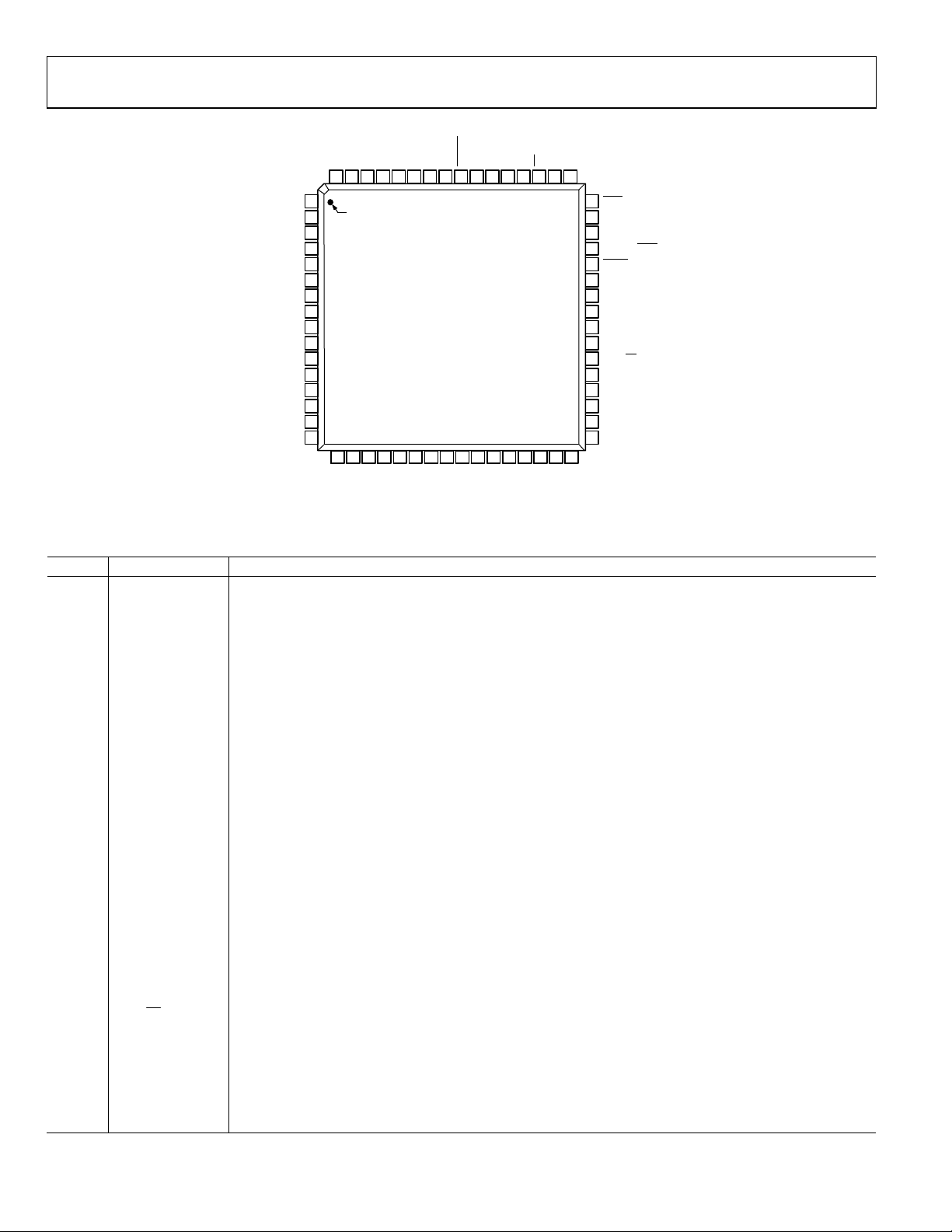
Figure 10. ADE5566/ADE5569 Pin Configuration
Table 14. Pin Function Descriptions
Pin No. Mnemonic Description
1 COM3/FP27 Common Output 3/LCD Segment Output 27. COM3 is used for the LCD backplane.
2 COM2/FP28 Common Output 2/LCD Segment Output 28. COM2 is used for the LCD backplane.
3 COM1 Common Output 1. COM1 is used for the LCD backplane.
4 COM0 Common Output 0. COM0 is used for the LCD backplane.
5 P1.2/FP25/ZX General-Purpose Digital I/O Port 1.2/LCD Segment Output 25/ZX Output.
6 P1.3/T2EX/FP24 General-Purpose Digital I/O Port 1.3/Timer 2 Control Input/LCD Segment Output 24.
7 P1.4/T2/FP23 General-Purpose Digital I/O Port 1.4/Timer 2 Input/LCD Segment Output 23.
8 P1.5/FP22 General-Purpose Digital I/O Port 1.5/LCD Segment Output 22.
9 P1.6/FP21 General-Purpose Digital I/O Port 1.6/LCD Segment Output 21.
10 P1.7/FP20 General-Purpose Digital I/O Port 1.7/LCD Segment Output 20.
11 P0.1/FP19 General-Purpose Digital I/O Port 0.1/LCD Segment Output 19.
12 P2.0/FP18 General-Purpose Digital I/O Port 2.0/LCD Segment Output 18.
13 P2.1/FP17 General-Purpose Digital I/O Port 2.1/LCD Segment Output 17.
14 P2.2/FP16 General-Purpose Digital I/O Port 2.2/LCD Segment Output 16.
15 LCDVC Output Port for LCD Levels. This pin should be decoupled with a 470 nF capacitor.
16 LCDVP2
Analog Output. A 100 nF capacitor should be connected between this pin and LCDVP1 for the internal LCD
charge pump device.
17, 18 LCDVB, LCDVA Output Ports for LCD Levels. These pins should be decoupled with a 470 nF capacitor.
19 LCDVP1
Analog Output. A 100 nF capacitor should be connected between this pin and LCDVP2 for the internal LCD
charge pump device.
20 to 35 FP15 to FP0 LCD Segment Output 15 to LCD Segment Output 0.
36 P1.1/TxD General-Purpose Digital I/O Port 1.1/Transmitter Data Output (Asynchronous).
37 P1.0/RxD General-Purpose Digital I/O Port 1.0/Receive Data Input (Asynchronous).
38
/T1/RxD2 General-Purpose Digital I/O Port 0.7/Slave Select When SPI Is in Slave Mode/Timer 1 Input/Receive Data
P0.7/SS
Input 2 (Asynchronous).
39 P0.6/SCLK/T0 General-Purpose Digital I/O Port 0.6/Clock Output for I2C or SPI Port/Timer 0 Input.
40 P0.5/MISO/ZX General-Purpose Digital I/O Port 0.5/Data Input for SPI Port/ZX Output.
41 P0.4/MOSI/SDATA General-Purpose Digital I/O Port 0.4/Data Output for SPI Port/I2C-Compatible Data Line.
42 P0.3/CF2
General-Purpose Digital I/O Port 0.3/Calibration Frequency Logic Output 2. The CF2 logic output gives
instantaneous active, reactive, or apparent power or I
information.
rms
Rev. C | Page 18 of 156
ADE5166/ADE5169/ADE5566/ADE5569
Pin No. Mnemonic Description
43 P0.2/CF1
44
45
/P2.3/TxD2 Serial Download Mode Enable/General-Purpose Digital Output Port 2.3/Transmitter Data Output 2
SDEN
BCTRL/INT1
/P0.0 Digital Input for Battery Control/External Interrupt Input 1/General-Purpose Digital I/O Port 0.0. This logic
46 XTAL2
47 XTAL1
48
INT0
49, 50 VP, VN
51
Input for Emulation. When held high, this input enables the device to fetch code from internal program
EA
52, 53 IP, IN
54 AGND Ground Reference for Analog Circuitry.
55 FP26 LCD Segment Output 26.
56
57 REF
58 V
59 V
RESET
IN/OUT
BAT
INTA
60 VDD
61 V
62 V
SWOUT
INTD
63 DGND Ground Reference for Digital Circuitry.
64 V
DCIN
General-Purpose Digital I/O Port 0.2/Calibration Frequency Logic Output 1. The CF1 logic output gives
instantaneous active, reactive, or apparent power or I
information.
rms
(Asynchronous). This pin is used to enable serial download mode through a resistor when pulled low on
power-up or reset. On reset, this pin momentarily becomes an input, and the status of the pin is sampled.
If there is no pull-down resistor in place, the pin momentarily goes high, and then user code is executed.
If the pin is pulled down on reset, the embedded serial download/debug kernel executes, and this pin
remains low during the internal program execution. After reset, this pin can be used as a digital output port
pin (P2.3) or as Transmitter Data Output 2 (asynchronous).
input connects V
open, the connection between V
DD
or V
BAT
to V
internally when set to logic high or logic low, respectively. When left
SWOUT
or V
BAT
and V
DD
is selected internally.
SWOUT
A crystal can be connected across this pin and XTAL1 (see the XTAL1 pin description) to provide a clock
source. The XTAL2 pin can drive one CMOS load when an external clock is supplied at XTAL1 or by the gate
oscillator circuit. An internal 6 pF capacitor is connected to this pin.
An external clock can be provided at this logic input. Alternatively, a tuning fork crystal can be connected
across XTAL1 and XTAL2 to provide a clock source. The clock frequency for specified operation is 32.768 kHz.
An internal 6 pF capacitor is connected to this pin.
External Interrupt Input 0.
Analog Inputs for Voltage Channel. These inputs are fully differential voltage inputs with a maximum
differential level of ±500 mV for specified operation. This channel also has an internal PGA.
memory locations. The ADE5566/ADE5569 do not support external code memory. This pin should not be left
floating.
Analog Inputs for Current Channel. These inputs are fully differential voltage inputs with a maximum
differential level of ±500 mV for specified operation. This channel also has an internal PGA.
Reset Input, Active Low.
Access to On-Chip Voltage Reference. The on-chip reference has a nominal value of 1.2 V ± 0.1% and a typical
temperature coefficient of 50 ppm/°C maximum. This pin should be decoupled with a 1 μF capacitor in
parallel with a ceramic 100 nF capacitor.
Power Supply Input from the Battery with a 2.4 V to 3.7 V Range. This pin is connected internally to V
when
DD
the battery is selected as the power supply.
Access to On-Chip 2.5 V Analog LDO. No external active circuitry should be connected to this pin. This pin
should be decoupled with a 10 μF capacitor in parallel with a ceramic 100 nF capacitor.
3.3 V Power Supply Input from the Regulator. This pin is connected internally to V
when the regulator is
SWOUT
selected as the power supply. This pin should be decoupled with a 10 μF capacitor in parallel with a ceramic
100 nF capacitor.
3.3 V Power Supply Output. This pin provides the supply voltage for the LDOs and the internal circuitry. This
pin should be decoupled with a 10 μF capacitor in parallel with a ceramic 100 nF capacitor.
Access to On-Chip 2.5 V Digital LDO. No external active circuitry should be connected to this pin. This pin
should be decoupled with a 10 μF capacitor in parallel with a ceramic 100 nF capacitor.
Analog Input for DC Voltage Monitoring. The maximum input voltage on this pin is V
with respect to
SWOUT
AGND. This pin is used to monitor the preregulated dc voltage.
Rev. C | Page 19 of 156
ADE5166/ADE5169/ADE5566/ADE5569
TYPICAL PERFORMANCE CHARACTERISTICS
2.0
GAIN = 1
1.5
INTEGRATOR OFF
INTERNAL REFERENCE
1.0
MID CLASS C
2.0
GAIN = 1
INTEGRATOR OFF
1.5
INTERNAL REFERENCE
1.0
0.5
+25°C; PF = 1
0
–0.5
ERROR (% of Reading)
–1.0
–1.5
–2.0
0.1 1 10 100
+85°C; PF = 1
–40°C; PF = 1
MID CLASS C
CURRENT CHANNEL (% of Full Scale)
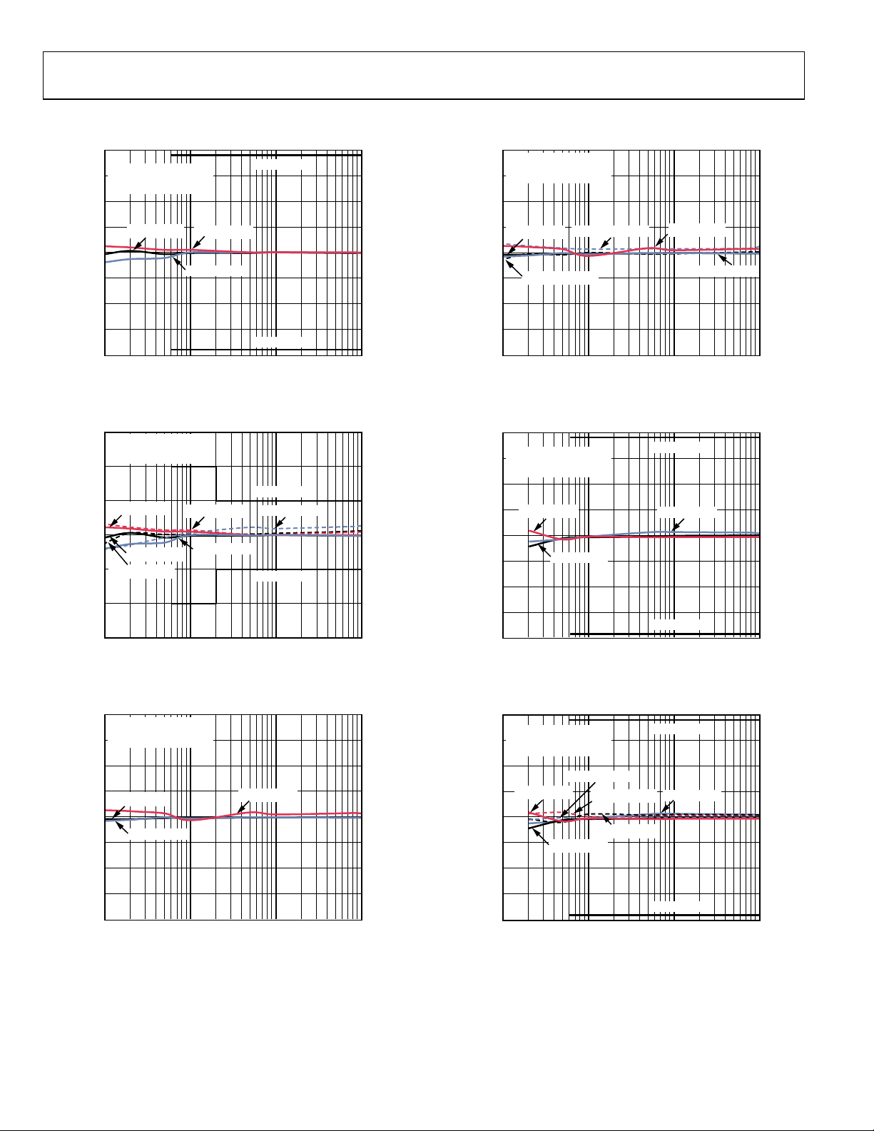
Figure 11. Active Energy Error as a Percentage of Reading (Gain = 1)
over Temperature with Internal Reference, Integrator Off
1.5
GAIN = 1
INTEGRATOR OFF
INTERNAL REFERENCE
1.0
0.5
+85°C; PF = 1
0
+25°C; PF = 1
–0.5
+25°C; PF = 0.5
ERROR (% of Read ing)
–1.0
–1.5
0.1 1 10 100
+85°C; PF = 0.5
–40°C; PF = 1
CURRENT CHANNEL (% of Full Scale)
MID CLASS C
–40°C; PF = 0. 5
MID CLASS C
Figure 12. Active Energy Error as a Percentage of Reading (Gain = 1)
over Power Factor with Internal Reference, Integrator Off
2.0
GAIN = 1
INTEGRATOR OFF
1.5
INTERNAL REFERENCE
1.0
–0.5
ERROR (% of Reading)
–1.0
0.5
0
+25°C; PF = 0
–40°C; PF = 0
+85°C; PF = 0
0.5
+25°C; PF = 0
0
+25°C; PF = 0.866
–0.5
ERROR (% of Reading)
–1.0
–1.5
–2.0
0.1 1 10 100
07411-126
–40°C; PF = 0 .866
CURRENT CHANNEL (% of Full Scale)
+85°C; PF = 0
–40°C; PF = 0
07411-129
Figure 14. Reactive Energy Error as a Percentage of Reading (Gain = 1)
over Power Factor with Internal Reference, Integrator Off
2.0
GAIN = 1
1.5
INTEGRATOR OFF
INTERNAL REFERENCE
1.0
0.5
+85°C; PF = 1
0
–0.5
ERROR (% of Reading)
–1.0
–1.5
–2.0
0.1 1 10 100
07411-127
+25°C; PF = 1
CURRENT CHANNEL (% of Full Scale)
MID CLASS C
–40°C; PF = 1
MID CLASS C
07411-130
Figure 15. Current RMS Error as a Percentage of Reading (Gain = 1)
over Temperature with Internal Reference, Integrator Off
2.0
GAIN = 1
1.5
INTEGRATOR OFF
INTERNAL REFERENCE
1.0
0.5
+85°C; PF = 1
0
–0.5
ERROR (% of Read ing)
–1.0
–40°C; PF = 0. 5
+85°C; PF = 0.5
+25°C; PF = 0.5
+25°C; PF = 1
MID CLASS C
–40°C; PF = 1
–1.5
–2.0
0.1 1 10 100
CURRENT CHANNEL (% of Full Scale)
Figure 13. Reactive Energy Error as a Percentage of Reading (Gain = 1)
over Temperature with Internal Reference, Integrator Off
07411-128
Rev. C | Page 20 of 156
–1.5
–2.0
0.1 1 10 100
CURRENT CHANNEL (% of Full Scale)
MID CLASS C
Figure 16. Current RMS Error as a Percentage of Reading (Gain = 1)
over Power Factor with Internal Reference, Integrator Off
07411-131
ADE5166/ADE5169/ADE5566/ADE5569
0.5
GAIN = 1
INTEGRATOR OFF
0.4
INTERNAL REFERENCE
0.3
0.2
I
; 3.13V
0.1
0
–0.1
–0.2
ERROR (% of Read ing)
–0.3
–0.4
–0.5
RMS
0.1 1 10 100
I
; 3.3V
RMS
I
; 3.43V
RMS
CURRENT CHANNEL (% of Full Scale)
V
; 3.3V
RMS
V
; 3.43V
RMS
V
; 3.13V
RMS
07411-132
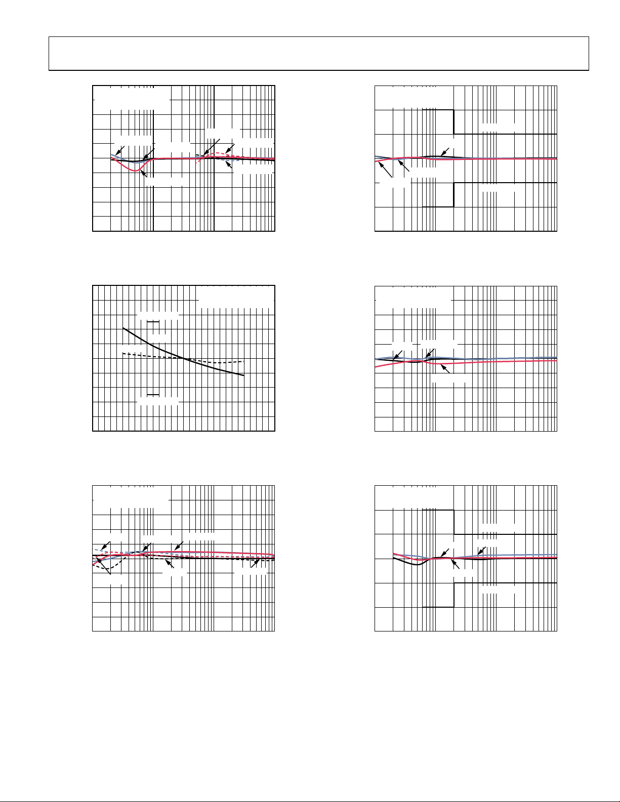
Figure 17. Voltage and Current RMS Error as a Percentage of Reading
(Gain = 1) over Power Supply with Internal Reference
1.0
0.8
0.6
0.4
0.2
0
–0.2
–0.4
ERROR (% of Read ing)
–0.6
–0.8
–1.0
40 45 50 55 60 65 70
MID CLASS B
PF = 1
PF = 0.5
MID CLASS B
LINE FREQ UENCY (Hz)
GAIN = 1
INTEGRATOR OFF
INTERNAL REFERENCE
07411-133
Figure 18. Active Energy Error as a Percentage of Reading (Gain = 1)
over Frequency with Internal Reference, Integrator Off
0.5
GAIN = 1
INTEGRATOR OFF
0.4
INTERNAL REFE RENCE
0.3
0.2
W; 3.13V
0.1
0
–0.1
W; 3.43V
–0.2
ERROR (% of Reading)
–0.3
–0.4
–0.5
0.1 1 10 100
VAR; 3.13V
CURRENT CHANNEL (% of Full Scale)
W; 3.3V
VAR; 3.43V
VAR; 3.3V
07411-134
Figu re 19. Active and Reactive Energy Error as a Percentage of Reading (Gain = 1)
over Power Supply with Internal Reference, Integrator Off
1.5
GAIN = 8
INTEGRATOR OFF
INTERNAL REF ERENCE
1.0
0.5
0
PF = –0.5
–0.5
ERROR (% of Read ing)
–1.0
–1.5
0.1 1 10 100
PF = +1
PF = +0.5
CURRENT CHANNEL (% of Full Scale)
MID CLASS C
MID CLASS C
Figure 20. Active Energy Error as a Percentage of Reading (Gain = 8)
over Power Factor with Internal Reference, Integrator Off
1.0
GAIN = 8
INTEGRATOR OFF
0.8
INTERNAL REF ERENCE
0.6
0.4
0.2
0
–0.2
–0.4
ERROR (% of Read ing)
–0.6
–0.8
–1.0
0.1 1 10 100
PF = +0.866
PF = 0
PF = –0.866
CURRENT CHANNEL (% of Full Scale)
Figure 21. Reactive Energy Error as a Percentage of Reading (Gain = 8)
over Power Factor with Internal Reference, Integrator Off
1.5
GAIN = 8
INTEGRATOR OFF
INTERNAL REF ERENCE
1.0
0.5
PF = +1
0
–0.5
ERROR (% of Reading)
–1.0
–1.5
0.1 1 10 100
CURRENT CHANNEL (% of Full Scale)
PF = –0.5
MID CLASS C
PF = +0.5
MID CLASS C
Figure 22. Current RMS Error as a Percentage of Reading (Gain = 8)
over Power Factor with Internal Reference, Integrator Off
07411-135
07411-136
07411-137
Rev. C | Page 21 of 156
ADE5166/ADE5169/ADE5566/ADE5569
2.0
GAIN = 16
INTEGRATOR OFF
1.5
INTERNAL REF ERENCE
1.0
0.5
+25°C;PF = 1
0
–0.5
ERROR (% of Reading)
–1.0
–1.5
–2.0
0.1 1 10 100
–40°C;PF = 1
CURRENT CHANNEL (% of Full Scale)
MID CLASS C
+85°C;PF = 1
MID CLASS C
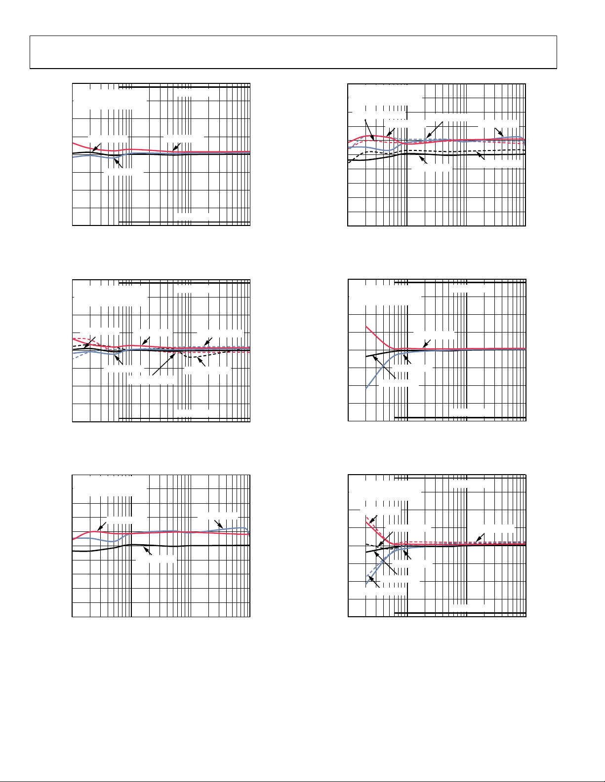
Figure 23. Active Energy Error as a Percentage of Reading (Gain = 16)
over Temperature with Internal Reference, Integrator Off
2.0
GAIN = 16
INTEGRATOR OFF
1.5
INTERNAL REFERENCE
1.0
+25°C;PF = 1
0.5
0
+85°C;PF = 1
MID CLASS C
–40°C;PF = 0.5
07411-138
1.0
GAIN = 16
INTEGRATOR OFF
0.8
INTERNAL REFERENCE
0.6
+85°C; PF = 0.866
0.4
0.2
0
–0.2
–0.4
ERROR (% of Reading)
–0.6
–0.8
–1.0
0.1 1 10 100
+85°C; PF = 0
CURRENT CHANNEL (% of Full Scale)
–40°C; PF = 0.866
+25°C; PF = 0
–40°C; PF = 0
+25°C; PF = 0.866
Figure 26. Reactive Energy Error as a Percentage of Reading (Gain = 16)
over Power Factor with Internal Reference, Integrator Off
2.0
GAIN = 16
INTEGRATOR OFF
1.5
INTERNAL REFERENCE
1.0
0.5
0
+85°C;PF = 1
MID CLASS C
07411-141
–0.5
ERROR (% of Read ing)
–1.0
–1.5
–2.0
0.1 1 10 100
–40°C;PF = 1
+85°C;PF = 0.5
CURRENT CHANNEL (% of Full Scale)
+25°C;PF = 0.5
MID CLASS C
Figure 24. Active Energy Error as a Percentage of Reading (Gain = 16)
over Power Factor with Internal Reference, Integrator Off
1.0
GAIN = 16
INTEGRATOR OFF
0.8
INTERNAL REFERENCE
0.6
0.4
0.2
0
–0.2
–0.4
ERROR (% of Read ing)
–0.6
–0.8
–1.0
0.1 1 10 100
+85°C; PF = 0
+25°C; PF = 0
CURRENT CHANNEL (% of Full Scale)
–40°C; PF = 0
Figure 25. Reactive Energy Error as a Percentage of Reading (Gain = 16)
over Temperature with Internal Reference, Integrator Off
–0.5
ERROR (% of Reading)
–1.0
–1.5
–2.0
0.1 1 10 100
07411-139
–40°C;PF = 1
+25°C;PF = 1
MID CLASS C
CURRENT CHANNEL (% of Fu ll Scale)
07411-142
Figure 27. Current RMS Error as a Percentage of Reading (Gain = 16)
over Temperature with Internal Reference, Integrator Off
2.0
GAIN = 16
INTEGRATOR OFF
1.5
INTERNAL REFERENCE
1.0
+85°C;PF = 1
0.5
0
–0.5
ERROR (% of Read ing)
–1.0
–1.5
–2.0
0.1 1 10 100
07411-140
+25°C;PF = 0.5
–40°C;PF = 1
+25°C;PF = 1
–40°C;PF = 0.5
CURRENT CHANNEL (% of Fu ll Scale)
MID CLASS C
+85°C;PF = 0.5
MID CLASS C
07411-143
Figure 28. Current RMS Error as a Percentage of Reading (Gain = 16)
over Power Factor with Internal Reference, Integrator Off
Rev. C | Page 22 of 156
ADE5166/ADE5169/ADE5566/ADE5569
2.0
GAIN = 16
INTEGRATOR ON
1.5
INTERNAL REFERENCE
1.0
–40°C;PF = 1
0.5
0
–0.5
ERROR (% of Read ing)
–1.0
+85°C;PF = 1
–40°C;PF = 0.5
+25°C; PF = 1
+25°C; PF = 0.5
MID CLASS C
+85°C;PF = 0.5
2.0
GAIN = 16
INTEGRATOR ON
1.5
INTERNAL REFERENCE
1.0
0.5
0
–0.5
ERROR (% of Reading)
–1.0
+25°C; PF = 0.5
+25°C; PF = 1
+85°C;PF = 1
–40°C; PF = 0 .5
–40°C; PF = 1
MID CLASS C
+85°C;PF = 0.5
–1.5
–2.0
0.1 1 10 100
CURRENT CHANNEL (% of Fu ll Scale)
MID CLASS C
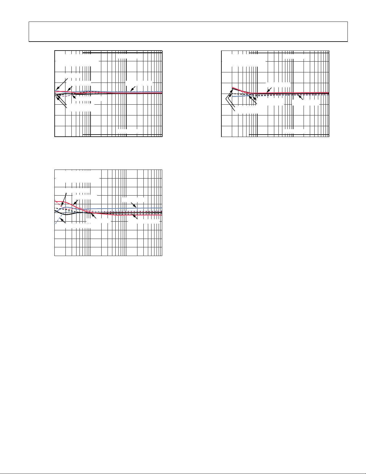
Figure 29. Active Energy Error as a Percentage of Reading (Gain = 16)
over Power Factor with Internal Reference, Integrator On
1.0
GAIN = 16
INTEGRATOR ON
0.8
INTERNAL REFERENCE
0.6
+85°C; PF = 0.866
0.4
0.2
0
–0.2
–0.4
ERROR (% of Read ing)
–0.6
–0.8
–1.0
0.1 1 10 100
+85°C; PF = 0
+25°C; PF = 0
–40°C; PF = 0.866
CURRENT CHANNEL (% of Full Scale)
–40°C; PF = 0
+25°C; PF = 0.866
Figu re 30. Reactive Energy Error as a Percentage of Reading (Gain = 16)
over Power Factor with Internal Reference, Integrator On
–1.5
–2.0
0.1 1 10 100
07411-144
CURRENT CHANNEL (% of Fu ll Scale)
MID CLASS C
07411-146
Figure 31. Current RMS Error as a Percentage of Reading (Gain = 16)
over Power Factor with Internal Reference, Integrator On
07411-145
Rev. C | Page 23 of 156

ADE5166/ADE5169/ADE5566/ADE5569
TERMINOLOGY
Measurement Error
The error associated with the energy measurement made by the
ADE5166/ADE5169/ADE5566/ADE5569 is defined by the following formula:
Measurement Error =
⎛
⎜
⎜
⎝
Phase Error Between Channels
The digital integrator and the high-pass filter (HPF) in the current
channel have a nonideal phase response. To offset this phase
response and equalize the phase response between channels,
two phase correction networks are placed in the current channel:
one for the digital integrator and the other for the HPF. The phase
correction networks correct the phase response of the corresponding component and ensure a phase match between the
current channel and the voltage channel to within ±0.1° over a
range of 45 Hz to 65 Hz with the digital integrator off. With the
digital integrator on, the phase is corrected to within ±0.4° over
a range of 45 Hz to 65 Hz.
Power Supply Rejection (PSR)
PSR quantifies the ADE5166/ADE5169/ADE5566/ADE5569
measurement error as a percentage of reading when the power
supplies are varied. For the ac PSR measurement, a reading at
nominal supplies (3.3 V) is taken. A second reading is obtained
−
EnergyTrue
⎞
EnergyTrueRegisterEnergy
⎟
%100×
⎟
⎠
with the same input signal levels when an ac signal (100 mV rms/
120 Hz) is introduced onto the supplies. Any error introduced
by this ac signal is expressed as a percentage of the reading (see
the Measurement Error definition).
For the dc PSR measurement, a reading at nominal supplies
(3.3 V) is taken. A second reading is obtained with the same
input signal levels when the supplies are varied ±5%. Any error
introduced is expressed as a percentage of the reading.
ADC Offset Error
ADC offset error is the dc offset associated with the analog
inputs to the ADCs. It means that, with the analog inputs
connected to AGND, the ADCs still see a dc analog input
signal. The magnitude of the offset depends on the gain and
input range selection. However, when HPF1 is switched on,
the offset is removed from the current channel, and the power
calculation is not affected by this offset. The offsets can be
removed by performing an offset calibration (see the Analog
Inputs section).
Gain Error
Gain error is the difference between the measured ADC output
code (minus the offset) and the ideal output code (see the Current
Channel ADC section and the Voltage Channel ADC section).
It is measured for each of the gain settings on the current channel
(1, 2, 4, 8, and 16). The difference is expressed as a percentage
of the ideal code.
Rev. C | Page 24 of 156

ADE5166/ADE5169/ADE5566/ADE5569
SPECIAL FUNCTION REGISTER (SFR) MAPPING
Table 15. SFR Mapping
Mnemonic Address Description
INTPR 0xFF
Interrupt pins configuration SFR
(see Tab le 17).
SCRATCH4 0xFE Scratch Pad 4 (see Table 25 ).
SCRATCH3 0xFD Scratch Pad 3 (see Table 24).
SCRATCH2 0xFC Scratch Pad 2 (see Table 23).
SCRATCH1 0xFB Scratch Pad 1 (see Table 22 ).
BATVTH 0xFA
Battery detection threshold
(see Tab le 53).
STRBPER 0xF9
Peripheral ADC strobe period
(see Tab le 50).
IPSMF 0xF8
Power management interrupt flag
(see Tab le 18).
TEMPCAL 0xF7
RTC temperature compensation
(see Table 133).
RTCCOMP 0xF6
RTC nominal compensation
(see Table 132).
BATPR 0xF5
Battery switchover configuration
(see Tab le 19).
PERIPH 0xF4
Peripheral configuration
(see Tab le 20).
DIFFPROG 0xF3
Temperature and supply delta
(see Tab le 51).
B 0xF0 Auxiliary math (see Tabl e 57).
VDCINADC 0xEF V
SBAUD2 0xEE
ADC value (see Table 54).
DCIN
Enhanced Serial Baud Rate Control 2
(see Table 148).
LCDSEGE2 0xED LCD Segment Enable 2 (see Table 101).
IPSME 0xEC
Power management interrupt enable
(see Tab le 21).
SBUF2 0xEB Serial Port 2 buffer (see Table 14 7 ).
SPISTAT 0xEA SPI interrupt status (see Table 155).
SPI2CSTAT 0xEA I2C interrupt status (see Table 1 5 9).
SPIMOD2 0xE9 SPI Configuration SFR 2 (see Table 154).
I2CADR 0xE9 I2C slave address (see Table 158).
SPIMOD1 0xE8 SPI Configuration SFR 1 (see Table 153).
I2CMOD 0xE8 I2C mode (see Table 157).
WAV2H 0xE7 Selection 2 sample MSB (see Ta ble 31).
WAV2 M 0xE 6
Selection 2 sample middle byte
(see Tab le 31).
WAV2L 0xE5 Selection 2 sample LSB (see Table 31).
WAV1H 0xE4 Selection 1 sample MSB (see Ta ble 31).
WAV1 M 0xE 3
Selection 1 sample middle byte
(see Tab le 31).
WAV1L 0xE2 Selection 1 sample LSB (see Table 31).
SCON2 0xE1
Serial Communications Control 2
(see Table 146).
ACC 0xE0 Accumulator (see Table 57).
BATADC 0xDF Battery ADC value (see Table 5 5).
MIRQSTH 0xDE Interrupt Status 3 (see Tab le 43).
MIRQSTM 0xDD Interrupt Status 2 (see Table 42).
MIRQSTL 0xDC Interrupt Status 1 (see Table 41).
MIRQENH 0xDB Interrupt Enable 3 (see Tab le 46).
MIRQENM 0xDA Interrupt Enable 2 (see Table 45).
Rev. C | Page 25 of 156
Mnemonic Address Description
MIRQENL 0xD9 Interrupt Enable 1 (see Tab le 44).
ADCGO 0xD8 Start ADC measurement (see Table 52 ).
TEMPADC 0xD7 Temperature ADC value (see Table 56 ).
IRMSH 0xD6 I
IRMSM 0xD5
measurement MSB (see Table 31 ).
rms
measurement middle byte
I
rms
(see Tab le 31).
IRMSL 0xD4 I
VRMSH 0xD3 V
VRMSM 0xD2
measurement LSB (see Table 31 ).
rms
measurement MSB (see Table 31 ).
rms
measurement middle byte
V
rms
(see Tab le 31).
VRMSL 0xD1 V
measurement LSB (see Table 31 ).
rms
PSW 0xD0 Program status word (see Tab le 58).
TH2 0xCD Timer 2 high byte (see Table 120).
TL2 0xCC Timer 2 low byte (see Table 121).
RCAP2H 0xCB
Timer 2 reload/capture high byte
(see Table 122).
RCAP2L 0xCA
Timer 2 reload/capture low byte
(see Table 123).
T2CON 0xC8 Timer/Counter 2 control (see Table 115).
EADRH 0xC7 Flash high byte address (see Table 110).
EADRL 0xC6 Flash low byte address (see Table 109).
POWCON 0xC5 Power control (see Ta ble 26).
KYREG 0xC1 Key (see Tabl e 126).
WDCON 0xC0 Watchdog timer (see Tabl e 88).
STCON 0xBF Stack boundary (see Table 65).
EDATA 0xBC Flash data (see Table 108).
PROTKY 0xBB Flash protection key (see Tab le 107).
FLSHKY 0xBA Flash key (see Table 106).
ECON 0xB9 Flash control (see Table 105).
IP 0xB8 Interrupt priority (see Table 82 ).
SPH 0xB7 Stack pointer high (see Ta ble 64 ).
PINMAP2 0xB4
Port 2 weak pull-up enable
(see Table 164).
PINMAP1 0xB3
Port 1 weak pull-up enable
(see Table 163).
PINMAP0 0xB2
Port 0 weak pull-up enable
(see Table 162).
LCDCONY 0xB1 LCD Configuration Y (see Table 94 ).
CFG 0xAF Configuration (see Table 66).
LCDDAT 0xAE LCD data (see Table 100).
LCDPTR 0xAC LCD pointer (see Ta ble 99).
IEIP2 0xA9
Interrupt Enable and Priority 2
(see Tab le 83).
IE 0xA8 Interrupt enable (see Tab le 81).
DPCON 0xA7 Data pointer control (see Table 7 9).
RTCDAT 0xA4 RTC pointer data (see Table 131).
RTCPTR 0xA3 RTC pointer address (see Table 1 3 0).
TIMECON2 0xA2 RTC Configuration 2 (see Table 129).
TIMECON 0xA1 RTC configuration (see Table 128).
P2 0xA0 Port 2 (see Table 167).
EPCFG 0x9F
Extended port configuration
(see Table 161).

ADE5166/ADE5169/ADE5566/ADE5569
Mnemonic Address Description
SBAUDT 0x9E
SBAUDF 0x9D
LCDCONX 0x9C LCD Configuration X (see Table 9 2).
SPI2CRx 0x9B SPI/I2C receive buffer (see Table 152).
SPI2CTx 0x9A SPI/I2C transmit buffer (see Table 151).
SBUF 0x99 Serial port buffer (see Table 141).
SCON 0x98
LCDSEGE 0x97 LCD segment enable (see Table 98 ).
LCDCLK 0x96 LCD clock (see Table 95).
LCDCON 0x95 LCD configuration (see Tab le 91).
MDATH 0x94
MDATM 0x93
MDATL 0x92
Enhanced serial baud rate control
(see Table 142).
UART timer fractional divider
(see Table 143).
Serial communications control
(see Table 140).
Energy measurement pointer data MSB
(see Tab le 31).
Energy measurement pointer data
middle byte (see Table 31).
Energy measurement pointer data LSB
(see Tab le 31).
Mnemonic Address Description
MADDPT 0x91
P1 0x90 Port 1 (see Table 166).
TH1 0x8D Timer 1 high byte (see Table 118).
TH0 0x8C Timer 0 high byte (see Table 116).
TL1 0x8B Timer 1 low byte (see Table 119).
TL0 0x8A Timer 0 low byte (see Table 117).
TMOD 0x89
TCON 0x88
PCON 0x87 Program control (see Table 5 9).
DPH 0x83 Data pointer high (see Table 61 ).
DPL 0x82 Data pointer low (see Table 6 0).
SP 0x81 Stack pointer (see Tabl e 63).
P0 0x80 Port 0 (see Table 165).
Energy measurement pointer address
(see Tab le 30).
Timer/Counter 0 and Timer/Counter 1
mode (see Table 113).
Timer/Counter 0 and Timer/Counter 1
control (see Table 114).
Rev. C | Page 26 of 156
ADE5166/ADE5169/ADE5566/ADE5569
POWER MANAGEMENT
The ADE5166/ADE5169/ADE5566/ADE5569 have elaborate
power management circuitry that manages the regular power
supply to battery switchover and power supply failures.
Table 16. Power Management SFRs
SFR Address R/W Mnemonic Description
0xEC R/W IPSME Power management interrupt enable (see Tab le 21).
0xF5 R/W BATPR Battery switchover configuration (see Tabl e 19).
0xF8 R/W IPSMF Power management interrupt flag (see Table 18).
0xFF R/W INTPR Interrupt pins configuration (see Table 17).
0xF4 R/W PERIPH Peripheral configuration (see Table 20).
0xC5 R/W POWCON Power control (see Table 26).
0xFB R/W SCRATCH1 Scratch Pad 1 (see Table 2 2).
0xFC R/W SCRATCH2 Scratch Pad 2 (see Table 2 3).
0xFD R/W SCRATCH3 Scratch Pad 3 (see Table 24 ).
0xFE R/W SCRATCH4 Scratch Pad 4 (see Table 25 ).
POWER MANAGEMENT REGISTER DETAILS
Table 17. Interrupt Pins Configuration SFR (INTPR, Address 0xFF)
Bit Mnemonic Default Description
7 Reserved N/A Reserved.
[6:5] FSEL 00 Sets RTC calibration output frequency and calibration window.
FSEL Result (Calibration Window, Frequency)
00 30.5 sec, 1 Hz
01 30.5 sec, 512 Hz
10 0.244 sec, 500 Hz
11 0.244 sec, 16 kHz
4 Reserved N/A Reserved.
[3:1] INT1PRG 000
0 INT0PRG 0
1
X = don’t care
Controls the function of INT1
INT1PRG Result
X001 GPIO enabled
X011 BCTRL enabled
01X1
11X1
Controls the function of INT0
INT0PRG Result
0
1
INT1
INT1
INT0
INT0
Writing to the Interrupt Pins Configuration SFR (INTPR, Address 0xFF)
To protect the RTC from runaway code, a key must be written to the key SFR (KYREG, Address 0xC1) to obtain write access to the
INTPR SFR. The KYREG SFR (see Table 126) should be set to 0xEA to unlock the INTPR SFR and reset to 0 after a timekeeping register is
written to. The RTC registers can be written using the following 8052 assembly code:
MOV KYREG, #0EAh
MOV INTPR, #080h
.
input disabled
input enabled
.
input disabled
input enabled
The power management functionalities can be accessed directly
through the 8052 power management SFRs (see Table 1 6).
Rev. C | Page 27 of 156

ADE5166/ADE5169/ADE5566/ADE5569
Table 18. Power Management Interrupt Flag SFR (IPSMF, Address 0xF8)
Bit Bit Address Mnemonic Default Description
7 0xFF FPSR 0
Power supply restored interrupt flag. Set when the V
This occurs when the source of V
changes from V
SWOUT
6 0xFE FPSM 0 PSM interrupt flag. Set when an enabled PSM interrupt condition occurs.
5 0xFD FSAG 0 Voltage SAG interrupt flag. Set when an ADE energy measurement SAG condition occurs.
4 0xFC Reserved 0 This bit must be kept at 0 for proper operation.
3 0xFB FVADC 0
ADC monitor interrupt flag. Set when V
V
DCIN
DCIN
measurement is ready.
2 0xFA FBAT 0
monitor interrupt flag. Set when V
V
BAT
falls below BATVTH or when V
BAT
ready.
1 0xF9 FBSO 0 Battery switchover interrupt flag. Set when V
0 0xF8 FVDCIN 0 V
monitor interrupt flag. Set when V
DCIN
SWOUT
falls below 1.2 V.
DCIN
Table 19. Battery Switchover Configuration SFR (BATPR, Address 0xF5)
Bit Mnemonic Default Description
[7:2] Reserved 0 These bits must be kept at 0 for proper operation.
[1:0] BATPRG 0 Control bits for battery switchover.
BATPRG Result
00 Battery switchover enabled on low VDD
01 Battery switchover enabled on low VDD and low V
1X1 Battery switchover disabled
1
X = don’t care.
power supply has been restored.
DD
to VDD.
BAT
changes by VDCIN_DIFF or when the V
measurement is
BAT
switches from VDD to V
DCIN
BAT
.
DCIN
Table 20. Peripheral Configuration SFR (PERIPH, Address 0xF4)
Bit Mnemonic Default Description
7 RX2FLAG 0 If set, indicates that an RxD2 edge event has triggered wake-up from PSM2.
6 VSWSOURCE 1 Indicates the power supply that is internally connected to V
0 = V
1 = V
is connected to V
SWOUT
is connected VDD.
SWOUT
BAT
.
SWOUT
.
5 VDD_OK 1 If set, indicates that the VDD power supply is ready for operation.
4 PLL_FLT 0
If set, indicates that a PLL fault occurred where the PLL lost lock. Set the PLLACK bit (Bit 7) in the start
ADC measurement SFR (ADCGO, Address 0xD8) to acknowledge the fault and clear the PLL_FLT bit
(see Tab le 52).
3 REF_BAT_EN 0
Set this bit to enable the internal voltage reference in PSM2 mode. This bit should be set if LCD is on
in the PSM1 and PSM2 modes.
2 Reserved 0 This bit must be kept at 0 for proper operation.
[1:0] RXPROG 0
Controls the function of the P0.7/SS
/T1/RxD2 pin.
RXPROG Result
00 GPIO
01 RxD2 with wake-up disabled
11 RxD2 with wake-up enabled
Table 21. Power Management Interrupt Enable SFR (IPSME, Address 0xEC)
Bit Mnemonic Default Description
7 EPSR 0 Enables a PSM interrupt when the power supply restored interrupt flag (FPSR) is set.
6 Reserved 0 Reserved.
5 ESAG 0 Enables a PSM interrupt when the voltage SAG interrupt flag (FSAG) is set.
4 Reserved 0 This bit must be kept at 0 for proper operation.
3 EVADC 0 Enables a PSM interrupt when the V
2 EBAT 0 Enables a PSM interrupt when the V
ADC monitor interrupt flag (FVADC) is set.
DCIN
monitor interrupt flag (FBAT) is set.
BAT
1 EBSO 0 Enables a PSM interrupt when the battery switchover interrupt flag (FBSO) is set.
0 EVDCIN 0 Enables a PSM interrupt when the V
monitor interrupt flag (FVDCIN) is set.
DCIN
Rev. C | Page 28 of 156

ADE5166/ADE5169/ADE5566/ADE5569
Table 22. Scratch Pad 1 SFR (SCRATCH1, Address 0xFB)
Bit Mnemonic Default Description
[7:0] SCRATCH1 0 Value can be written/read in this register. This value is maintained in all the power saving modes.
Table 23. Scratch Pad 2 SFR (SCRATCH2, Address 0xFC)
Bit Mnemonic Default Description
[7:0] SCRATCH2 0 Value can be written/read in this register. This value is maintained in all the power saving modes.
Table 24. Scratch Pad 3 SFR (SCRATCH3, Address 0xFD)
Bit Mnemonic Default Description
[7:0] SCRATCH3 0 Value can be written/read in this register. This value is maintained in all the power saving modes.
Table 25. Scratch Pad 4 SFR (SCRATCH4, Address 0xFE)
Bit Mnemonic Default Description
[7:0] SCRATCH4 0 Value can be written/read in this register. This value is maintained in all the power saving modes.
Clearing the Scratch Pad Registers (SCRATCH1, Address 0xFB to SCRATCH4, Address 0xFE)
Note that these scratch pad registers are cleared only when the part loses VDD and V
Table 26. Power Control SFR (POWCON, Address 0xC5)
Bit Mnemonic Default Description
7 Reserved 1 Reserved.
6 METER_OFF 0
Set this bit to turn off the modulators and energy metering DSP circuitry to reduce power if metering
functions are not needed in PSM0 mode.
5 Reserved 0 This bit should be kept at 0 for proper operation.
4 COREOFF 0 Set this bit to shut down the core and enter PSM2 mode if in the PSM1 operating mode.
3 Reserved 0 Reserved.
[2:0] CD 010 Controls the core clock frequency, f
CD Result (f
CORE
CORE
. f
CORE
in MHz)
000 4.096
001 2.048
010 1.024
011 0.512
100 0.256
101 0.128
110 0.064
111 0.032
.
BAT
= 4.096 MHz/2CD.
Writing to the Power Control SFR (POWCON, Address 0xC5)
Writing data to the power control SFR (POWCON, Address 0xC5) involves writing 0xA7 into the key SFR (KYREG, Address 0xC1),
which is described in Table 126, followed by a write to the POWCON SFR. For example,
MOV KYREG,#0A7h ;Write KYREG to 0xA7 to get write access to the POWCON SFR
MOV POWCON,#10h ;Shut down the core
Rev. C | Page 29 of 156
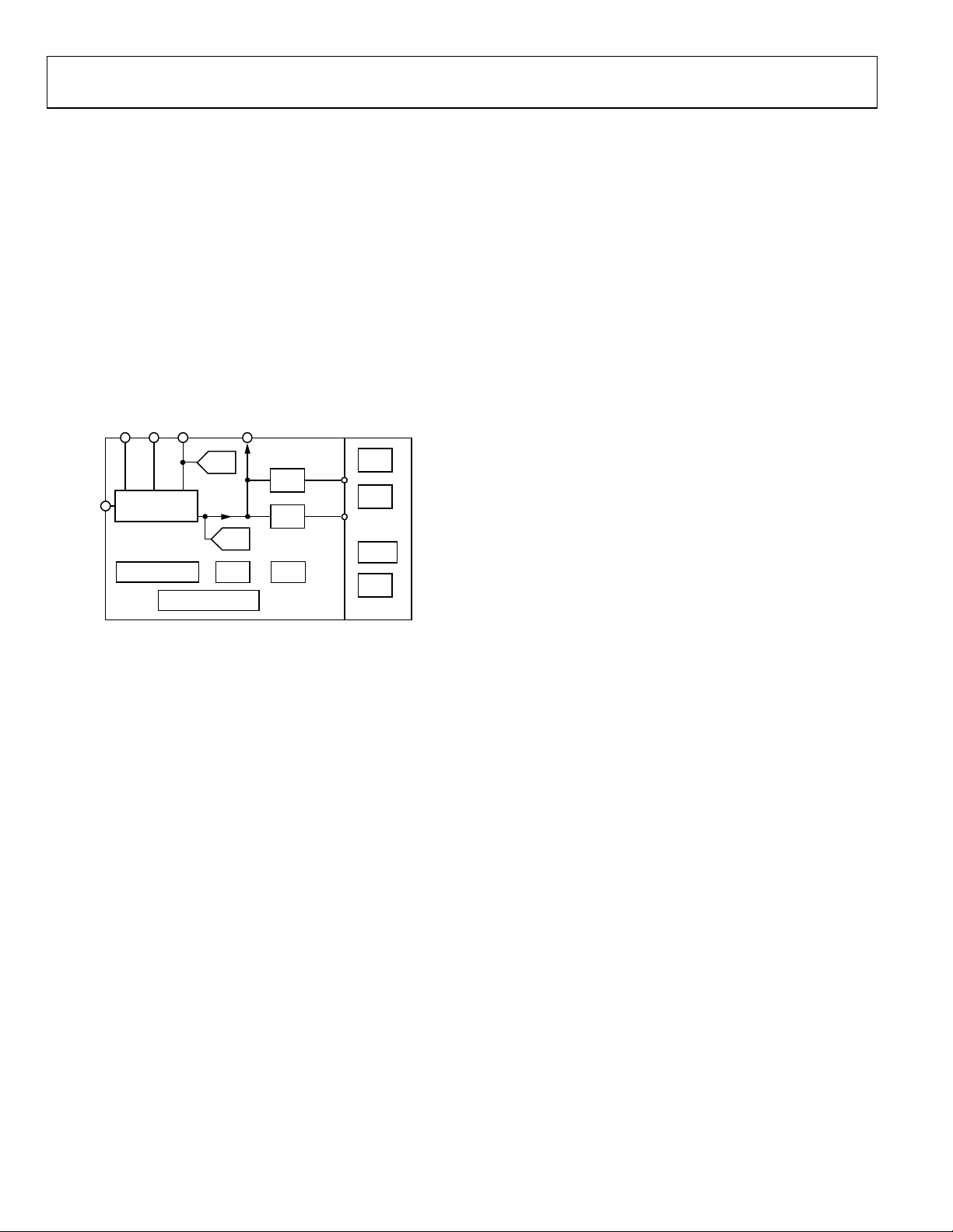
ADE5166/ADE5169/ADE5566/ADE5569
V
V
POWER SUPPLY ARCHITECTURE
The ADE5166/ADE5169/ADE5566/ADE5569 have two power
supply inputs, V
supply at V
DD
and V
DD
for full operation. A battery backup, or secondary
. They require only a single 3.3 V power
BAT
power supply, with a maximum of 3.7 V can be connected to the
input. Internally, the ADE5166/ADE5169/ADE5566/
V
BAT
ADE5569 connect V
DD
or V
BAT
to V
, which is used to derive
SWOUT
power for the ADE5166/ADE5169/ADE5566/ADE5569 circuitry.
The V
supply (V
output pin reflects the voltage at the internal power
SWOUT
) and has a maximum output current of 6 mA. This
SWOUT
pin can also be used to power a limited number of peripheral components. The 2.5 V analog supply (V
the core logic (V
V
. Figure 32 shows the ADE5166/ADE5169/ADE5566/
SWOUT
) are derived by on-chip linear regulators from
INTD
) and the 2.5 V supply for
INTA
ADE5569 power supply architecture.
BCTRL
DCINVDDVBAT
POWER SUPPLY
MANAGEMENT
SCRATCH PAD LCD RTC
TEMPERATURE ADC
Figure 32. Power Supply Architecture
V
ADC
SW
ADC
SWOUT
LDO
LDO
V
INTD
V
3.3V
INTA
MCU
ADE
SPI/I2C
UART
2.5V
7411-011
The ADE5166/ADE5169/ADE5566/ADE5569 provide automatic
battery switchover between V
level detected at V
DD
or V
and V
DD
. In addition, the BCTRL input can be
DCIN
based on the voltage
BAT
used to trigger a battery switchover. The conditions for switching
V
from VDD to V
SWOUT
Battery Switchover section. V
and back to VDD are described in the
BAT
is an input pin that can be con-
DCIN
nected to a dc signal of 0 V to 3.3 V. This input is intended for
power supply supervisory purposes and does not provide power
to the ADE5166/ADE5169/ADE5566/ADE5569 circuitry (see
the Battery Switchover section).
BATTERY SWITCHOVER
The ADE5166/ADE5169/ADE5566/ADE5569 monitor VDD,
, and V
V
BAT
can be configured based on the status of the V
pin. Battery switchover is enabled by default. Setting Bit 1 in the
battery switchover configuration SFR (BATPR, Address 0xF5)
disables battery switchover so that V
V
(see Tabl e 19 ). The source of V
SWOUT
in the peripheral configuration SFR (PERIPH, Address 0xF4),
which is described in Ta bl e 2 0 . Bit 6 is set when V
nected to V
The battery switchover functionality provided by the ADE5166/
ADE5169/ADE5566/ADE5569 allows a seamless transition from
to V
V
DD
. Automatic battery switchover from VDD to V
DCIN
, V
DD
is always connected to
DD
is indicated by Bit 6
SWOUT
and cleared when V
DD
. An automatic battery switchover option ensures a
BAT
is connected to V
SWOUT
, or BCTRL
DCIN
is con-
SWOUT
BAT
BAT
.
stable power supply to the ADE5166/ADE5169/ADE5566/
ADE5569, as long as the external battery voltage is above 2.75 V.
It allows continuous code execution even while the internal power
supply is switching from V
metering ADCs are not available when V
DD
to V
and back. Note that the energy
BAT
is used for V
BAT
SWOUT
.
Power supply management (PSM) interrupts can be enabled to
indicate when battery switchover occurs and when the V
power
DD
supply is restored (see the Power Supply Management (PSM)
Interrupt section).
Switching from VDD to V
BAT
The following three events switch the internal power supply
(V
SWOUT
• V
from V
) from VDD to V
< 1.2 V. When V
DCIN
to V
DD
:
BAT
falls below 1.2 V, V
DCIN
. This event is enabled when the BATPRG
BAT
SWOUT
switches
bits (Bits[1:0]) in the battery switchover configuration SFR
(BATPR, Address 0xF5) are set to 0b01.
• V
< 2.75 V. When VDD falls below 2.75 V, V
DD
from V
DD
to V
. This event is enabled when the BATPRG
BAT
SWOUT
switches
bits in the BATPR SFR are cleared.
• Falling edge on BCTRL. When the battery control pin,
BCTRL, goes low, V
external switchover signal can trigger a switchover to V
switches from VDD to V
SWOUT
BAT
. This
BAT
at any time. Setting the INT1PRG bits (Bits[3:1]) to 0bX01 in
the interrupt pins configuration SFR (INTPR, Address 0xFF)
enables the BCTRL pin (see Tabl e 17 ).
Switching from V
To s wit c h V
SWOUT
to VDD
BAT
from V
to VDD, all of the following events
BAT
must be true:
• V
> 2.75 V. V
DD
switches back to VDD after VDD remains
SWOUT
above 2.75 V.
• V
> 1.2 V and VDD > 2.75 V. If the low V
DCIN
is enabled, V
above 1.2 V and V
switches to VDD after V
SWOUT
remains above 2.75 V.
DD
DCIN
DCIN
condition
remains
• Rising edge on BCTRL. If the battery control pin is enabled,
V
switches back to VDD after BCTRL is high, and the
SWOUT
first or second bullet point is satisfied.
POWER SUPPLY MANAGEMENT (PSM) INTERRUPT
The power supply management (PSM) interrupt alerts the 8052
core of power supply events. The PSM interrupt is disabled by
default. Setting Bit 1 (EPSM) in the Interrupt Enable and Priority 2
SFR (IEIP2, Address 0xA9) enables the PSM interrupt (see
Tabl e 83 ).
The power management interrupt enable SFR (IPSME,
Address 0xEC) controls the events that result in a PSM interrupt
(see Tabl e 21 ).
Figure 33 illustrates how the PSM interrupt vector is shared among
the PSM interrupt sources. The PSM interrupt flags are latched
and must be cleared by writing to the power management interrupt
flag SFR (IPSMF, Address 0xF8), as described in Ta b le 18 .
Rev. C | Page 30 of 156
 Loading...