

Complete, 12-Bit, 45 MHz
K
FEATURES
Pin-compatible upgrade for the AD9945
45 MHz correlated double sampler (CDS) with variable gain
6 dB to 42 dB, 10-bit variable gain amplifier (VGA)
Low noise optical black clamp circuit
Preblanking function
12-bit, 45 MHz ADC
No missing codes guaranteed
3-wire serial digital interface
3 V single-supply operation
Space-saving, 32-lead, 5 mm × 5 mm LFCSP
APPLICATIONS
Digital still cameras
Digital video camcorders
PC cameras
Portable CCD imaging devices
CCTV cameras
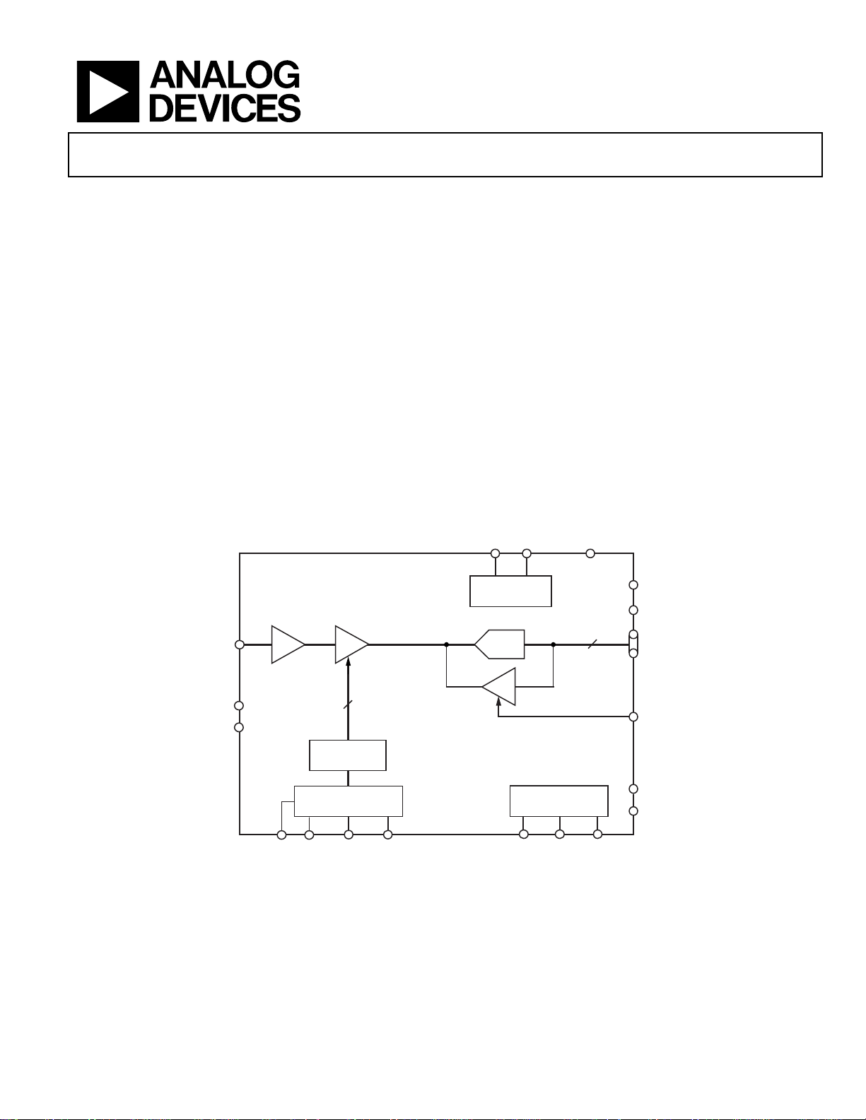
FUNCTIONAL BLOCK DIAGRAM
CCD Signal Processor
ADDI7100
GENERAL DESCRIPTION
The ADDI7100 is a complete analog signal processor for chargecoupled device (CCD) applications. It features a 45 MHz,
single-channel architecture designed to sample and condition
the outputs of interlaced and progressive scan area CCD arrays.
The signal chain for the ADDI7100 consists of a correlated double
sampler (CDS), a digitally controlled variable gain amplifier
(VGA), a black level clamp, and a 12-bit ADC.
The internal registers are programmed through a 3-wire serial
digital interface. Programmable features include gain adjustment,
black level adjustment, input clock polarity, and power-down
modes. The ADDI7100 operates from a single 3 V power supply,
typically dissipates 125 mW, and is packaged in a space-saving,
32-lead LFCSP.
REFT
REFB
PBL
CCDIN
AVD D
AVS S
ADDI7100
−3dB, 0dB,
+3dB, +6dB
CDS
VD
6dB TO 42dB
VGA
10
CONTROL
REGISTERS
DIGITAL
INTERFACE
BAND GAP
REFERENCE
12-BIT
ADC
CLP
INTERNAL
SDATASCKSL
Figure 1.
12
TIMING
DATACLKSHDSHP
DRVDD
DRVSS
DOUT
D0 TO D11
CLPOB
DVDD
DVSS
07608-001
Rev. C
Information furnished by Analog Devices is believed to be accurate and reliable. However, no
responsibility is assumed by Analog Devices for its use, nor for any infringements of patents or other
rights of third parties that may result from its use. Specifications subject to change without notice. No
license is granted by implication or otherwise under any patent or patent rights of Analog Devices.
Trademarks and registered trademarks are the property of their respective owners.
One Technology Way, P.O. Box 9106, Norwood, MA 02062-9106, U.S.A.
Tel: 781.329.4700 www.analog.com
Fax: 781.461.3113 ©2008–2010 Analog Devices, Inc. All rights reserved.

ADDI7100
TABLE OF CONTENTS
Features .............................................................................................. 1
Applications ....................................................................................... 1
General Description ......................................................................... 1
Functional Block Diagram .............................................................. 1
Revision History ............................................................................... 2
Specifications ..................................................................................... 3
General Specifications ................................................................. 3
Digital Specifications ................................................................... 3
System Specifications ................................................................... 4
Timing Specifications .................................................................. 5
Absolute Maximum Ratings ............................................................ 7
Thermal Resistance ...................................................................... 7
ESD Caution .................................................................................. 7
Pin Configuration and Function Descriptions ............................. 8
Typical Performance Characteristics ............................................. 9
Equivalent Input Circuits .............................................................. 10
Terminology .................................................................................... 11
Circuit Description and Operation .............................................. 12
DC Restore .................................................................................. 12
Correlated Double Sampler (CDS) .......................................... 12
Optical Black Clamp .................................................................. 12
Analog-to-Digital Converter (ADC) ....................................... 13
Variable Gain Amplifier (VGA) ............................................... 13
Digital Data Outputs .................................................................. 13
Applications Information .............................................................. 14
Initial Power-On Sequence ....................................................... 15
Grounding and Decoupling Recommendations .................... 15
Serial Interface Timing .................................................................. 16
Complete Register Listing ............................................................. 17
Outline Dimensions ....................................................................... 19
Ordering Guide .......................................................................... 19
REVISION HISTORY
6/10—Rev. B to Rev. C
Changes to 0x0D Description and 0xFF Description in
Table 8 .............................................................................................. 18
9/09—Rev. A. to Rev. B
Changes to Features Section............................................................ 1
Changed Power-Down Mode to Full Standby Mode, Table 1 .... 3
Moved Timing Diagrams Section .................................................. 5
Changes to Table 4, Figure 3, and Figure 4 ................................... 5
Changes to Figure 9 Caption ......................................................... 10
Changes to Optical Black Clamp Section .................................... 12
Changes to Initial Power-On Sequence Section ......................... 15
Changes to Figure 16 ...................................................................... 16
Changes to Table 8 .......................................................................... 17
2/09—Rev. 0 to Rev. A
Changes to Serial Interface Timing Section ................................ 16
Changes to Figure 16 and Figure 17 ............................................. 16
10/08—Revision 0: Initial Version
Rev. C | Page 2 of 20
ADDI7100
SPECIFICATIONS
GENERAL SPECIFICATIONS
T
to T
MIN
Table 1.
Parameter Min Typ Max Unit
TEMPERATURE RANGE
Operating −25 +85 °C
Storage −65 +150 °C
POWER SUPPLY VOLTAGE
Analog, Digital, Digital Driver 2.7 3.6 V
POWER CONSUMPTION
Normal Operation 125 mW
Full Standby Mode 1 mW
MAXIMUM CLOCK RATE 45 MHz
DIGITAL SPECIFICATIONS
DRVDD = DVDD = 2.7 V, CL = 20 pF, unless otherwise noted.
Table 2.
Parameter Symbol Min Typ Max Unit
LOGIC INPUTS
High Level Input Voltage VIH 2.1 V
Low Level Input Voltage VIL 0.6 V
High Level Input Current IIH 10 μA
Low Level Input Current IIL 10 μA
Input Capacitance CIN 10 pF
LOGIC OUTPUTS
High Level Output Voltage, IOH = 2 mA VOH 2.2 V
Low Level Output Voltage, IOL = 2 mA VOL 0.5 V
, AVDD = DVDD = DRVDD = 3 V, f
MAX
= 45 MHz, unless otherwise noted.
SAMP
Rev. C | Page 3 of 20
ADDI7100
SYSTEM SPECIFICATIONS
T
to T
MIN
Table 3.
Parameter Test Conditions/Comments Min Typ Max Unit
CDS Input characteristics definition1
Allowable CCD Reset Transient 0.5 1.2 V
CDS Gain Accuracy VGA gain = 6 dB (Code 15, default value)
Maximum Input Range Before Saturation
Maximum CCD Black Pixel Amplitude Positive offset definition1
VARIABLE GAIN AMPLIFIER (VGA)
Gain Control Resolution 1024 Steps
Gain Monotonicity Guaranteed
Gain Range
BLACK LEVEL CLAMP MEASURED AT ADC OUTPUT
Clamp Level Resolution 2048 Steps
Clamp Level Measured at ADC output
ADC
Resolution 12 Bits
Differential Nonlinearity (DNL) −1.0 ±0.5 LSB
No Missing Codes Guaranteed
Full-Scale Input Voltage 2.0 V
VOLTAGE REFERENCE
Reference Top Voltage (REFT) 2.0 V
Reference Bottom Voltage (REFB) 1.0 V
SYSTEM PERFORMANCE Specifications include entire signal chain
Gain Accuracy
Peak Nonlinearity, 1 V Input Signal 6 dB total gain (default CDS, VGA) 0.1 %
Total Output Noise AC grounded input, 6 dB total gain 0.8 LSB rms
Power Supply Rejection (PSR) Measured with step change on supply 45 dB
1
Input signal characteristics are defined as shown in . Figure 2
, AVDD = DVDD = DRVDD = 3 V, f
MAX
= 45 MHz, unless otherwise noted.
SAMP
−3 dB CDS Gain −2.45 −2.95 −3.45 dB
0 dB CDS Gain Default setting 5.40 5.90 6.40 dB
+3 dB CDS Gain 8.65 9.15 9.65 dB
+6 dB CDS Gain 11.10 11.60 12.10 dB
0 dB CDS Gain Default setting 1.0 V p-p
−3 dB CDS Gain 1.4 V p-p
+6 dB CDS Gain 0.5 V p-p
0 dB CDS Gain Default setting −100 +200 mV
+6 dB CDS Gain −50 +100 mV
Minimum Gain (VGA Code 15) See Figure 13 for VGA curve 6.0 dB
Maximum Gain (VGA Code 1023)
See Variable Gain Amplifier (VGA)
42.0 dB
section for VGA gain equation
Minimum Clamp Level (Code 0) 0 LSB
Maximum Clamp Level (Code 1023) 511 LSB
Low Gain (VGA Code 15) 6 dB total gain (default CDS, VGA) 5.4 5.9 6.4 dB
Maximum Gain (VGA Code 1023) 41.4 41.9 42.4 dB
500mV TYP
RESET TRANSIENT
OPTICAL BLACK PI XEL
100mV TYP
INPUT SIG NAL RANGE
Figure 2.
Rev. C | Page 4 of 20
1V TYP
7608-002
ADDI7100
G
2
TIMING SPECIFICATIONS
CL = 20 pF, f
Table 4.
Parameter Symbol Min Typ Max Unit
SAMPLE CLOCKS
DATACLK, SHP, SHD Clock Period t
DATACLK High/Low Pulse Width t
SHP Pulse Width t
SHD Pulse Width t
CLPOB Pulse Width1 2 20 Pixels
SHP Rising Edge to SHD Falling Edge tS3 5.5 ns
SHP Rising Edge to SHD Rising Edge tS1 9 11 t
SHD Rising Edge to SHP Rising Edge tS2 9 11 t
SHD Rising Edge to SHP Falling Edge tS4 5.5 ns
Internal Clock Delay tID 4 ns
DATA OUTPUTS
Output Delay tOD 15 ns
Pipeline Delay 15 Cycles
SERIAL INTERFACE
Maximum SCK Frequency (Must Not Exceed Pixel Rate) f
SL to SCK Setup Time tLS 10 ns
SCK to SL Hold Time tLH 10 ns
SDATA Valid to SCK Rising Edge Setup tDS 10 ns
SCK Rising Edge to SDATA Valid Hold tDH 10 ns
1
Minimum CLPOB pulse width is for functional operation only. Wider typical pulses are recommended to achieve low noise clamp performance.
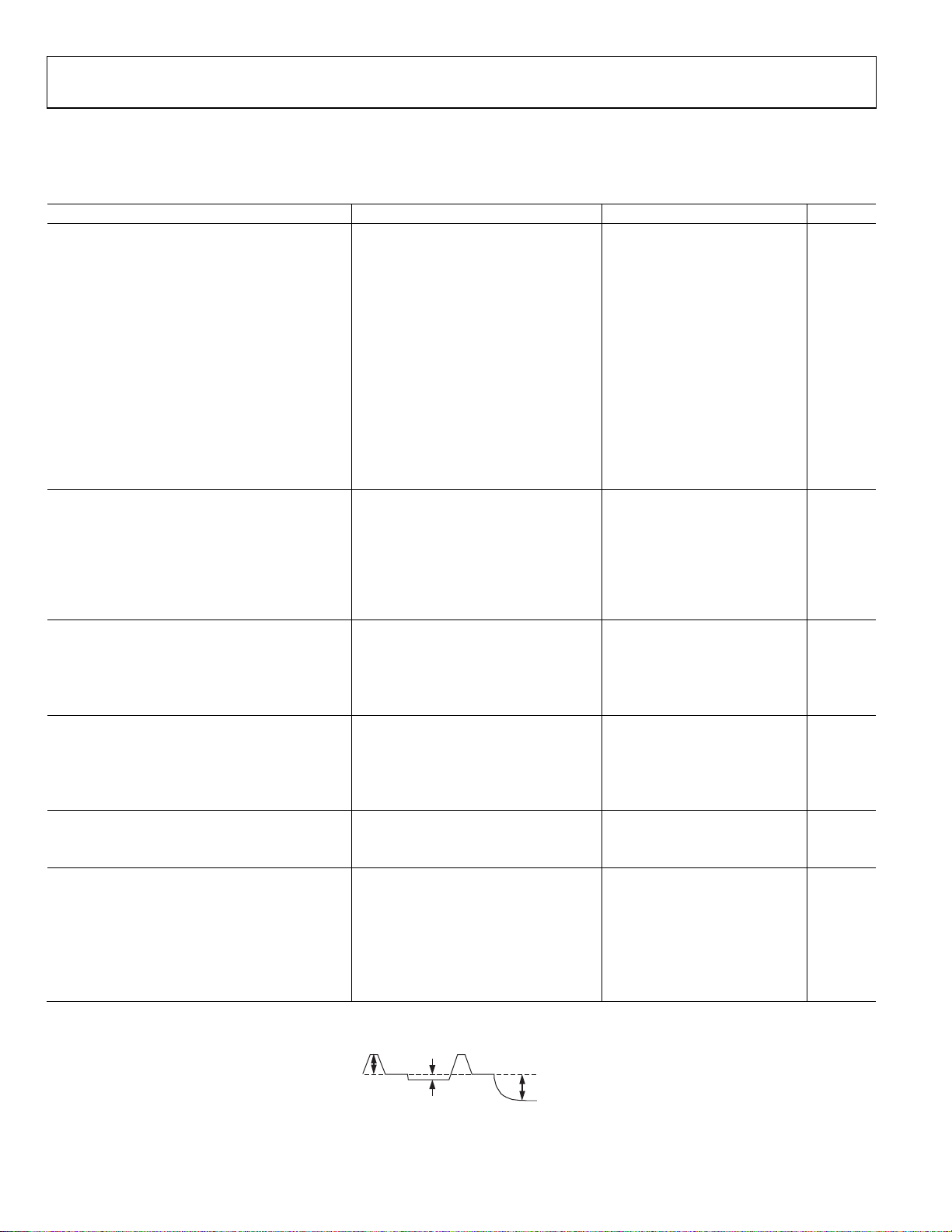
Timing Diagrams
= 45 MHz, unless otherwise noted. See Figure 3, Figure 4, and Figure 16.
SAMP
22 ns
CONV
9 11 ns
ADC
5.5 ns
SHP
5.5 ns
SHD
40 MHz
SCLK
− tS2 ns
CONV
− tS1 ns
CONV
CCD
SIGNAL
(CCDIN)
DATACLK
OUTPUT
DATA
NOTES
1. RECOMMENDED P LACEMENT FO R DATACLK RISI NG (ACTIVE) EDGE IS NEAR THE SHP OR SHD RI SIN
(ACTIVE) EDG E. THE BEST LOCATI ON FOR LOWEST NO ISE WI LL BE SYST EM DEPENDENT.
. CCD SIGNAL I S SAMPLED AT SHP AND SHD RISING EDGES.
SHP
SHD
t
ID
PIXEL N PIXEL
t
ID
t
t
S3
N – 15 N – 14 N – 13 N – 1 N
S4
t
OD
N + 1
t
t
S1
S2
t
CONV
PIXEL
N + 2
Figure 3. CCD Sampling Timing (Default Polarity Settings)
Rev. C | Page 5 of 20
PIXEL
N + 14
PIXEL
N + 15
07608-012
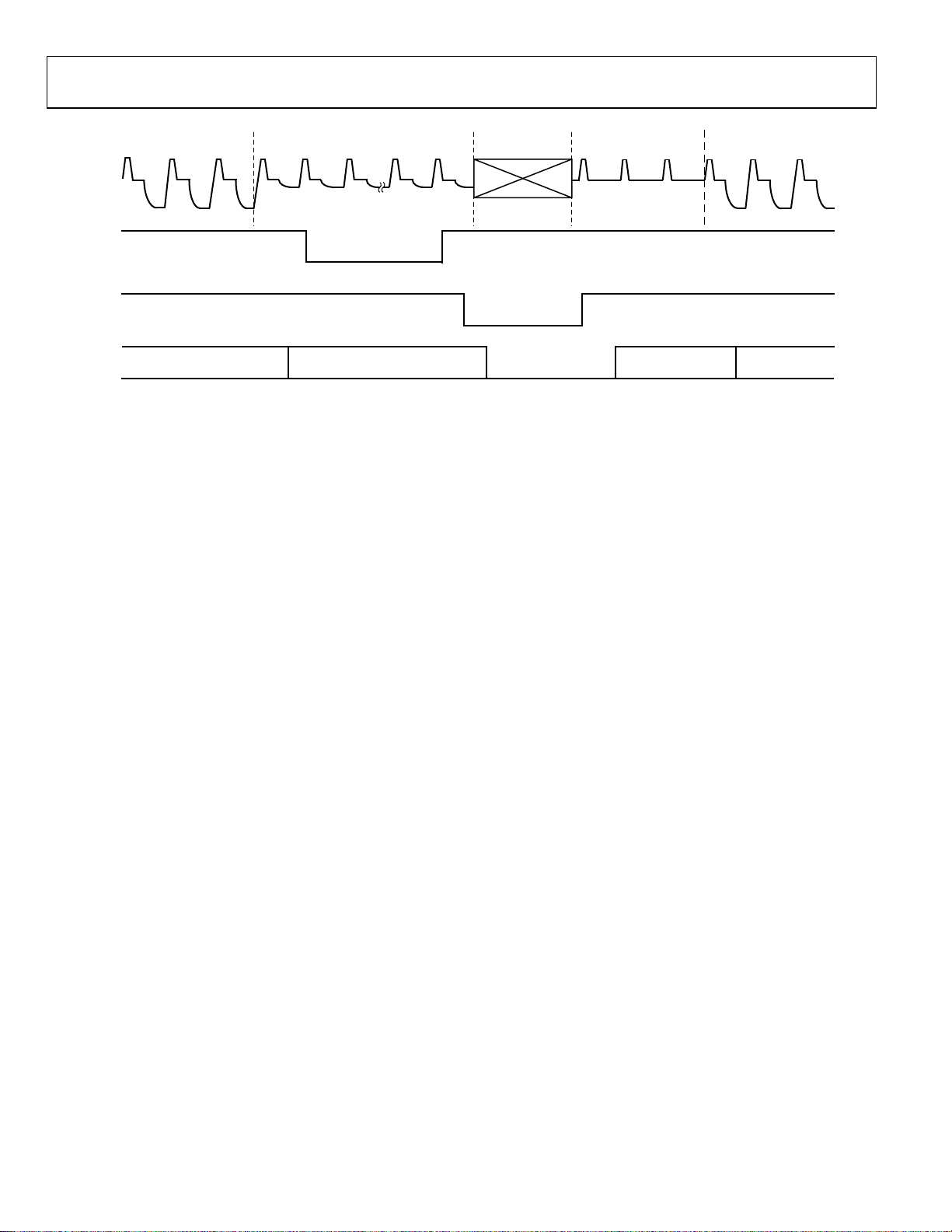
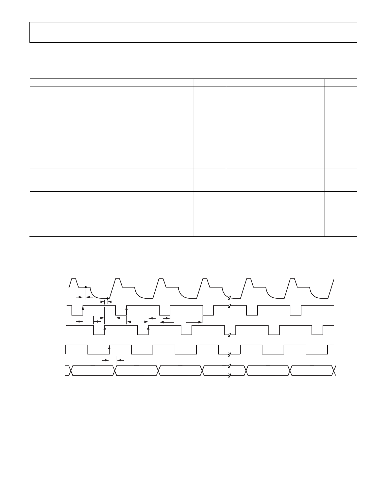
ADDI7100
A
L
2
3
O
EFFECTIVE PIXELS
CCD
SIGNAL
(CCDIN)
CLPOB
PBLK
UTPUT
DATA
NOTES
1. CLPOB AND PBLK SHOUL D BE ALIGNED W ITH THE CCD S IGNAL INPUT (CCDIN) .
CLPOB WI
. PBLK SIGNAL IS OPTI ONAL. KEEP THE PBLK PIN IN THE INACTI VE STATE IF NOT USED.
. DIGITAL OUTPUT DATA WILL BE ALL ZEROS DURING PBLK. OUTPUT DATA LATENCY IS FIFT EEN DATACLK CYCLES.
EFFECTIVE PIXEL DATA
L OVERWRITE PBLK. PBLK WILL NOT AFFECT CLAMP OPERATION IF OVERLAPPING WITH CLPOB.
OPTICAL BLACK PIXELS
ACTIVE
OB PIXEL DATA DUMMY BLACK EF FECTIVE DATA
HORIZONT
BLANKING
ACTIVE
L
Figure 4. Typical Clamp Timing (Default Polarity Settings)
DUMMY PIXELS EFFECTIVE PIXELS
07608-013
Rev. C | Page 6 of 20

ADDI7100
ABSOLUTE MAXIMUM RATINGS
Table 5.
Parameter Rating
AVDD to AVSS −0.3 V to +3.9 V
DVDD to DVSS −0.3 V to +3.9 V
DRVDD to DRVSS −0.3 V to +3.9 V
Digital Outputs to DRVSS −0.3 V to DRVDD + 0.3 V
SHP, SHD, DATACLK to DVSS −0.3 V to DVDD + 0.3 V
CLPOB, PBLK to DVSS −0.3 V to DVDD + 0.3 V
SCK, SL, SDATA to DVSS −0.3 V to DVDD + 0.3 V
REFT, REFB, CCDIN to AVSS −0.3 V to AVDD + 0.3 V
Junction Temperature 150°C
Lead Temperature (10 sec) 300°C
Stresses above those listed under Absolute Maximum Ratings
may cause permanent damage to the device. This is a stress
rating only; functional operation of the device at these or any
other conditions above those indicated in the operational
section of this specification is not implied. Exposure to absolute
maximum rating conditions for extended periods may affect
device reliability.
THERMAL RESISTANCE
θJA is specified for a device with the exposed bottom pad
soldered to the circuit board ground.
Table 6. Thermal Resistance
Package Type θJA Unit
32-Lead LFCSP 27.7 °C/W
ESD CAUTION
Rev. C | Page 7 of 20

ADDI7100
PIN CONFIGURATION AND FUNCTION DESCRIPTIONS
32 D1
31 D0
30 NC
29 NC
28 VD
27 SCK
26 SDATA
25 SL
D2 1
D3 2
D4 3
D5 4
D6 5
D7 6
D8 7
D9 8
NOTES
1. IT IS RECOMMENDED THAT THE EXPOSED
PAD BE SOLDERED TO THE GROUND PLANE
OF THE PCB.
2. NC = NO CONNECT.
PIN 1
INDICATOR
ADDI7100
TOP VIEW
(Not to Scale)
D11 10
D10 9
DRVSS 12
DRVDD 11
DVDD 13
DATACLK 14
DVSS 15
PBLK 16
24 REFB
23 REFT
22 CCDIN
21 AVSS
20 AVDD
19 SHD
18 SHP
17 CLPOB
07608-003
Figure 5. Pin Configuration
Table 7. Pin Function Descriptions
Pin No. Mnemonic Type1 Description
1 to 10 D2 to D11 DO Digital Data Outputs.
11 DRVDD P Digital Output Driver Supply.
12 DRVSS P Digital Output Driver Ground.
13 DVDD P Digital Supply.
14 DATACLK DI Digital Data Output Latch Clock.
15 DVSS P Digital Supply Ground.
16 PBLK DI Preblanking Clock Input.
17 CLPOB DI Black Level Clamp Clock Input.
18 SHP DI CDS Sampling Clock for CCD Reference Level.
19 SHD DI CDS Sampling Clock for CCD Data Level.
20 AVDD P Analog Supply.
21 AVSS P Analog Ground.
22 CCDIN AI Analog Input for CCD Signal.
23 REFT AO ADC Top Reference Voltage Decoupling.
24 REFB AO ADC Bottom Reference Voltage Decoupling.
25 SL DI Serial Digital Interface Load Pulse.
26 SDATA DI Serial Digital Interface Data Input.
27 SCK DI Serial Digital Interface Clock Input.
28 VD DI
Vertical Sync Input. Controls the update time of VD-updated registers. If this pin is not
needed, it should be tied to GND.
29, 30 NC NC Not Internally Connected.
31, 32 D0, D1 DO Digital Data Output.
1
AI = analog input, AO = analog output, DI = digital input, DO = digital output, P = power, and NC = no connect.
Rev. C | Page 8 of 20

ADDI7100
TYPICAL PERFORMANCE CHARACTERISTICS
200
180
160
140
120
100
80
POWER (mW)
60
40
20
0
10 22 36 45
3.6V
SAMPLE RATE ( MHz)
3.0V
2.7V
07608-018
Figure 6. Power vs. Sample Rate
3
2
1
0
–1
INL (LSB)
–2
–3
–4
–5
1
523
1045
1567
2089
2611
3133
262
784
1306
1828
CODE
2350
2872
3394
3655
3916
07608-017
Figure 8. Typical INL Performance
0.5
0.4
0.3
0.2
0.1
0
–0.1
DNL (LSB)
–0.2
–0.3
–0.4
–0.5
–0.6
1 539 1077 1615 2153 2691 3229 3767
270 808 1346 1884 2422 2960 3498
CODE
4036
07608-016
Figure 7. Typical DNL Performance
Rev. C | Page 9 of 20

ADDI7100
A
V
EQUIVALENT INPUT CIRCUITS
DVDD
DD
INPUT
330Ω
DVSS
07608-004
Figure 9. Digital Inputs
SHP, SHD, DATACLK, CLPOB, PBLK, SCK, SL, SDATA, and VD
DRVDD
D[0:11]
DRVSS
DATA
THREE-
STATE
DVDD
DVSS
Figure 10. Data Outputs
60Ω
AVS S
AVS S
07608-006
Figure 11. CCDIN (Pin 22)
07608-005
Rev. C | Page 10 of 20

ADDI7100
TERMINOLOGY
Differential Nonlinearity (DNL)
An ideal ADC exhibits code transitions that are exactly 1 LSB
apart. DNL is the deviation from this ideal value. Therefore,
every code must have a finite width. No missing codes guaranteed
to 12-bit resolution indicates that all 4096 codes, respectively,
must be present over all operating conditions.
Peak Nonlinearity
Peak nonlinearity, a full signal chain specification, refers to the
peak deviation of the output of the ADDI7100 from a true
straight line. The point used as zero scale occurs 0.5 LSB before
the first code transition. Positive full scale is defined as a level
that is 1.5 LSB beyond the last code transition. The deviation is
measured from the middle of each particular output code to the
true straight line. The error is then expressed as a percentage of
the 2 V ADC full-scale signal. The input signal is always gained
appropriately to fill the full-scale range of the ADC.
Tot a l O ut p ut Noi se
The rms output noise is measured using histogram techniques.
The standard deviation of the ADC output codes is calculated
in LSBs and represents the rms noise level of the total signal
chain at the specified gain setting. The output noise can be
converted to an equivalent voltage, using the relationship
1 LSB = (ADC Full Scale/2
where N is the bit resolution of the ADC. For example, 1 LSB of
the ADDI7100 is 0.5 mV.
N
codes)
Power Supply Rejection (PSR)
PSR is measured with a step change applied to the supply pins.
This represents a very high frequency disturbance on the power
supply of the ADDI7100. The PSR specification is calculated
from the change in the data outputs for a given step change in
the supply voltage.
Internal Delay for SHP/SHD
The internal delay (also called aperture delay) is the time delay
that occurs from the time a sampling edge is applied to the
ADDI7100 until the actual sample of the input signal is held.
Both SHP and SHD sample the input signal during the transition from low to high; therefore, the internal delay is measured
from the rising edge of each clock to the instant that the actual
internal sample is taken.
Rev. C | Page 11 of 20

ADDI7100
CIRCUIT DESCRIPTION AND OPERATION
DC RESTORE
0.1µF
CCDIN
SHP
SHD
–3dB, 0dB,
+3dB, +6dB
CDS
SHP
6dB TO 42d B
VGA
VGA GAIN
REGISTER
PBLK
DCBYP
DAC
10
Figure 12. CCD Mode Block Diagram
The ADDI7100 signal processing chain is shown in Figure 12.
Each processing step is essential for achieving a high quality
image from the raw CCD pixel data.
DC RESTORE
To reduce the large dc offset of the CCD output signal, a dc
restore circuit is used with an external 0.1 μF series coupling
capacitor. This circuit restores the dc level of the CCD signal
to approximately 1.5 V, which is compatible with the 3 V supply
of the ADDI7100.
CORRELATED DOUBLE SAMPLER (CDS)
The CDS circuit samples each CCD pixel twice to extract video
information and to reject low frequency noise. The timing
shown in Figure 3 illustrates how the two CDS clocks, SHP and
SHD, are used to sample the reference level and the data level,
respectively, of the CCD signal. The CCD signal is sampled on
the rising edges of SHP and SHD. Placement of these two clock
signals is critical for achieving the best performance from the
CCD. An internal SHP/SHD delay (t
internal propagation delays.
) of 4 ns is caused by
ID
INTERNAL
V
12-BIT
ADC
OPTICAL BL ACK
CLAMP
DIGITAL
FILTERING
REF
2V FULL SCALE
CLAMP LEVEL
11
REGISTER
DATA
OUTPUT
LATCH
CLPOB
CLAMP LEVEL
BLANK TO
ZERO OR
DATACLK
12
DOUT
D0 TO D11
PBLK
CLPOB
07608-010
OPTICAL BLACK CLAMP
The optical black clamp loop removes residual offsets in the
signal chain and tracks low frequency variations in the CCD
black level. During the optical black (shielded) pixel interval
on each line, the ADC output is compared with the fixed black
level reference selected by the user in the clamp level register
(Address 0x04). The resulting error signal is filtered to reduce
noise, and the correction value is applied to the ADC input
through a DAC. Normally, the optical black clamp loop is turned
on once per horizontal line, but this loop can be updated more
slowly to suit a particular application. If external digital clamping
is used during postprocessing, optical black clamping for the
ADDI7100 can be disabled using Address 0x00, Bit 2. When the
optical black clamp loop is disabled, the clamp level register can
still be used to provide programmable offset adjustment.
Note that if the CLPOB is disabled, higher VGA gain settings
reduce the dynamic range because the uncorrected offset in the
signal path is amplified.
Horizontal timing is shown in Figure 4. Align the CLPOB pulse
with the optical black pixels of the CCD. It is recommended that
the CLPOB pulse be used during valid CCD dark pixels. It is
recommended that the CLPOB pulse should be 20 pixels wide
to minimize clamp noise. Shorter pulse widths can be used, but
the ability of the loop to track low frequency variations in the
black level is reduced.
Rev. C | Page 12 of 20

ADDI7100
G
A
ANALOG-TO-DIGITAL CONVERTER (ADC)
The ADDI7100 uses a high performance ADC architecture
optimized for high speed and low power. Differential nonlinearity (DNL) performance is typically better than 0.5 LSB.
The ADC uses a 2 V full-scale input range.
VARIABLE GAIN AMPLIFIER (VGA)
The VGA stage provides a gain range of 6 dB to 42 dB, programmable with 10-bit resolution through the serial digital
interface. The minimum gain of 6 dB is needed to match a 1 V
input signal with the ADC full-scale range of 2 V. A plot of the
VGA gain curve is shown in Figure 13.
VGA Gain (dB) = (VGA Code × 0.0358 dB) + 5.4 dB
where Code is in the range of 0 to 1023.
42
36
30
24
GAIN (dB)
V
18
DIGITAL DATA OUTPUTS
By default, the digital output data is latched by the rising edge of
the DATACLK input. Output data timing is shown in Figure 3.
It is also possible to make the output data latch transparent,
immediately validating the data outputs from the ADC. Setting
the DOUTLATCH register (Address 0x01[5]) to 1 configures
the latch as transparent. The data outputs can also be disabled
by setting the DOUT_OFF register (Address 0x01[4]) to 1.
12
6
0
255
Figure 13. VGA Gain Curve
511 639 767 895 1023
383127
VGA GAIN REGISTER MODE
7608-011
Rev. C | Page 13 of 20

ADDI7100
APPLICATIONS INFORMATION
The ADDI7100 is a complete analog front-end (AFE) product
for digital still camera and camcorder applications. As shown in
Figure 14, the CCD image (pixel) data is buffered and sent to
the ADDI7100 analog input through a series input capacitor.
The ADDI7100 performs the dc restoration, CDS sampling,
gain adjustment, black level correction, and analog-to-digital
conversion. The digital output data of the ADDI7100 is then
processed by the image processing ASIC. The internal registers
of the ADDI7100—used to control gain, offset level, and other
functions—are programmed by the ASIC or by a microprocessor
through a 3-wire serial digital interface. A system timing generator
provides the clock signals for both the CCD and the AFE (see
Figure 14).
OUT
DIGITAL
OUTPUTS
SERIAL
INTERFACE
DIGITAL IMAGE
PROCESSING
ASIC
07608-014
CCD
V-DRIVER
V
OUT
BUFFER
0.1µF
CCD
TIMING
ADDI7100
CCDIN
GENERATOR
REGISTER
TIMING
ADC
DATA
CDS/CLAMP
TIMING
Figure 14. System Applications Diagram
NCNCVD
PIN 1
IDENTIFIER
ADDI7100
TOP VIEW
(Not to Scale)
3
SCK
SDATA
SL
24 REFB
23 REFT
22 CCDIN
21 AVSS
20 AVDD
19 SHD
18 SHP
17 CLPOB
1.0µF
1.0µF
0.1µF
0.1µF
CCDIN
3V
ANALOG
SUPPLY
INTERFACE
(SHOULD BE GRO UNDED IF NOT USED.)
VD OUTPUT FROM ASIC/DSP
D0
D1
D2 1
D3 2
D4 3
D5 4
D6 5
D7 6
D8 7
D9 8
SERIAL
32 31 30 29 28 27 26 25
910
12
DATA
OUTPUTS
3V
DRIVER
SUPPLY
NC = NO CONNECT (NO T INTERNALLY CONNECTED, MAY BE TIED TO GROUND OR L EFT FLOATING).
D10
0.1µF
D11
12 13 14 15 16
11
DVDD
DRVSS
DRVDD
DATACLK
0.1µF
DVSS
PBLK
3V
ANALOG
SUPPLY
5
CLOCK
INPUTS
07608-015
Figure 15. Recommended Circuit Configuration for CCD Mode
Rev. C | Page 14 of 20

ADDI7100
INITIAL POWER-ON SEQUENCE
After power-on, the ADDI7100 automatically resets all internal
registers to default values. Settling of the internal voltage reference takes approximately 1 ms to complete. During this time,
normal clock signals and serial write operations can take place,
but valid output data do not occur until the reference is fully
settled. When loading the desired register settings, the STARTUP
register (Address 0x05[1:0]) must be set to 0x3.
GROUNDING AND DECOUPLING RECOMMENDATIONS
As shown in Figure 15, a single ground plane is recommended
for the ADDI7100. This ground plane should be as continuous
as possible to ensure that all analog decoupling capacitors
provide the lowest possible impedance path between the power
and bypass pins and their respective ground pins. Place all
decoupling capacitors as close as possible to the package pins.
A single clean power supply is recommended for the ADDI7100,
but a separate digital driver supply can be used for DRVDD
(Pin 11). Always decouple DRVDD to DRVSS (Pin 12), which
should be connected to the analog ground plane. The advantages
of using a separate digital driver supply include using a lower
voltage (2.7 V) to match levels with a 2.7 V ASIC, and reducing
digital power dissipation and potential noise coupling. If the
digital outputs must drive a load larger than 20 pF, buffering is
the recommended method to reduce digital code transition
noise. Alternatively, placing series resistors close to the digital
output pins may also help to reduce noise.
Note that the exposed pad on the bottom of the package should
be soldered to the ground plane of the printed circuit board.
Rev. C | Page 15 of 20

ADDI7100
A
SERIAL INTERFACE TIMING
All ADDI7100 internal registers are accessed through a 3-wire
serial interface. Each register consists of an 8-bit address and
a 16-bit data-word. Both the address and the data-word are
written starting with the LSB. To write to each register, a 24-bit
operation is required, as shown in Figure 16. Although many
data-words are fewer than 16 bits wide, all 16 bits must be written
for each register. For example, if the data-word is only eight bits
wide, the upper eight bits are don’t care bits and must be filled
with zeros during the serial write operation. If fewer than 16 data
bits are written, the register is not updated with new data.
8-BIT ADDRESS 16-BIT DAT
Figure 17 shows a more efficient way to write to the registers,
using the ADDI7100 address autoincrement capability. Using
this method, the lowest desired address is written first, followed
by multiple 16-bit data-words. Each data-word is automatically
written to the address of the next highest register. By eliminating
the need to write each address, faster register loading is achieved.
Continuous write operations can start with any register location.
SDATA
NOTES
1. SDATA BITS ARE LATCHED ON SCK RI SING EDG ES. SCK CAN IDLE HIGH OR LO W BETWEEN WRITE OPERATIO NS.
2. ALL 24 BIT S MUST BE W RITTEN: 8 BITS FO R ADDRESS AND 16 BITS F OR DATA.
3. IF THE REGIST ER LENGTH IS LESS THAN 16 BITS, THEN ZERO S MUST BE USE D TO COMPLETE THE 16-BIT
DATA LENGTH.
4. NEW DATA VALUES ARE UPDATED IN THE SPECIF IED REGISTER LOCATION AT DIF FERENT T IMES, DEPENDING ON
THE PARTICULAR REGISTER WRITTEN TO.
A0 A1 A4 A5 A6 A7
SCK
SL
A2
t
DS
123
t
LS
D1 D2 D3 D13 D14 D15
A3
t
DH
D0
244 5 6 7 8 9 10 11 12 22 23
t
LH
07608-019
Figure 16. Serial Write Operation
SDATA
SCK
SL
DATA FOR STARTING
REGISTER ADDRES S
A0 A1 A2 A6 A7 D0 D1 D14 D15
1 24234 78910 23
A3
DATA FOR NEXT
REGISTER ADDRESS
D0 D1 D14 D15
2625 4039
D0
D2D1
424143
NOTES
1. MULTI PLE SEQUENTIAL REG ISTERS CAN BE L OADED CONTINUOUSLY.
2. THE FI RST (LOWEST ADDRESS ) REGIST ER ADDRESS IS W RITTEN, FOLLOWED BY MUL TIPLE 16-BIT DATA-W ORDS.
3. THE ADDRESS AUT OMATICAL LY INCREME NTS WIT H EACH 16-BIT DATA-WORD (ALL 16 BITS MUST BE WRIT TEN).
4. SL IS HELD LOW UNTIL THE LAST DESI RED REGIST ER HAS BEEN LOADED.
07608-020
Figure 17. Continuous Serial Write Operation
Rev. C | Page 16 of 20

ADDI7100
COMPLETE REGISTER LISTING
Note that when an address contains fewer than 16 data bits, all remaining bits must be written as zeros.
Table 8. AFE
Data
Address
0x00 [1:0] 0 SCK STANDBY
0x01 [0] 0 SCK SHPD_POL
0x02 [2:0] 0x1 SCK/VD CDSGAIN CDS gain setting:
0x03 [9:0] 0x0F SCK/VD VGAGAIN VGA gain, 6 dB to 42 dB (0.0358 dB per step)
0x04 [10:0] 0x1EC SCK/VD CLAMPLEVEL Optical black clamp level, 0 LSB to 511 LSB (0.25 LSB per step)
0x05 [1:0] 0 SCK STARTUP Must be set to 0x3 after power-up
0x06 [2:0] 0x6 SCK Test Test use only; must be set to 6
0x07 [0] 0 SCK Test Test use only; must be set to 0
0x08 [11:0] 0xFFF SCK Test Test use only; must be set to 0xFFF
0x09 [11:0] 0xFFF SCK Test Test use only; must be set to 0xFFF
0x0A [0] 0 SCK Test Test use only; must be set to 0
0x0B [0] 0 SCK SW_RST 1: software reset; automatically resets to 0 after software reset
0x0C [0] 0x1 SCK OUTCONTROL Data output control:
Bits
[2] 0x1 CLAMP_EN
[3] 0 FASTCLAMP
[4] 0 FASTUPDATE
[5] 0 PBLK_LVL
[6] 0 DCBYP
[8:7] 0x2 Test Test use only; must be set to 2
[10:9] 0x2 Test Test use only; must be set to 2
[1] 0 DATACLK_POL
[2] 0 CLP_POL
[3] 0 PBLK_POL
[4] 0 DOUT_OFF
[5] 0 DOUTLATCH
[6] 0 GRAY_EN 1: gray encode ADC outputs
[3:2] 0 Test Test use only; must be set to 0
[3] 0 Test Test use only; must be set to 0
[5:4] 0 Test Test use only; must be set to 0
Default
Value
Update
1
Typ e
Name Description
00: normal operation
01: reference standby
10: full standby
11: full standby
1: enable black clamp
0: disable black clamp
0: normal CLPOB settling
1: faster CLPOB settling
1: enable very fast clamping when CDS gain is changed
0: ignore CDS gain updates
0: blank to 0
1: blank to clamp level
0: normal dc restore operation
1: dc restore disabled during PBLK active
0: rising edge sample
1: falling edge sample
0: rising edge triggered
1: falling edge triggered
0: active low
1: active high
0: active low
1: active high
0: data outputs are driven
1: data outputs are disabled (high-Z)
0: retime data outputs with output latch (using DATACLK)
1: do not retime data outputs; output latch is transparent
0x0: −3 dB
0x1: 0 dB
0x2: +3 dB
0x3: +6 dB
0: make all outputs dc inactive
1: enable data outputs
Rev. C | Page 17 of 20

ADDI7100
Data
Address
Bits
0x0D [0] 0 SCK VD_POL
0x0E [6:0] 0 SCK REG_UPDATE Set the appropriate bits high to enable VD update of the selected registers:
0xFF [0] 0 SCK Test Test use only; do not access
1
SCK = register is immediately updated when the 16th data bit (D15) is written. VD = register is updated at the VD falling edge.
Default
Value
Update
Typ e1 Name Description
0: falling edge triggered
1: rising edge triggered
[0]: CDSGAIN (Register 0x02)
[1]: VGAGAIN (Register 0x03)
[2]: CLAMPLEVEL (Register 0x04)
[3]: test use only; must be set to 0
[4]: test use only; must be set to 0
[5]: test use only; must be set to 0
[6]: test use only; must be set to 0
Rev. C | Page 18 of 20

ADDI7100
OUTLINE DIMENSIONS
0.08
0.60 MAX
25
24
EXPOSED
PAD
(BOTTOM VIEW)
17
16
3.50 REF
PIN 1
32
9
FOR PROPER CONNECTION O F
THE EXPOSED PAD, REFER TO
THE PIN CONF IGURATIO N AND
FUNCTION DESCRIPTIO NS
SECTION OF THIS DATA SHEET.
INDICATOR
1
3.25
3.10 SQ
2.95
8
0.25 MIN
011708-A
5.00
PIN 1
INDICATO R
1.00
0.85
0.80
12° MAX
SEATING
PLANE
BSC SQ
TOP
VIEW
0.80 MAX
0.65 TYP
0.30
0.23
0.18
COMPLIANT TO JEDEC STANDARDS MO-220-VHHD-2
4.75
BSC SQ
0.20 REF
0.05 MAX
0.02 NOM
0.60 MAX
0.50
BSC
0.50
0.40
0.30
COPLANARIT Y
Figure 18. 32-Lead Lead Frame Chip Scale Package [LFCSP_VQ]
5 mm × 5 mm Body, Very Thin Quad
(CP-32-2)
Dimensions shown in millimeters
ORDERING GUIDE
Model1 Temperature Range Package Description Package Option
ADDI7100BCPZ −25°C to +85°C 32-Lead Lead Frame Chip Scale Package [LFCSP_VQ] CP-32-2
ADDI7100BCPZRL −25°C to +85°C 32-Lead Lead Frame Chip Scale Package [LFCSP_VQ] CP-32-2
1
Z = RoHS Compliant Part.
Rev. C | Page 19 of 20

ADDI7100
NOTES
©2008–2010 Analog Devices, Inc. All rights reserved. Trademarks and
registered trademarks are the property of their respective owners.
D07608-0-6/10(C)
Rev. C | Page 20 of 20
 Loading...