

A
www.BDTIC.com/ADI
Dual High Speed PECL Comparators
FEATURES
Differential PECL compatible outputs
700 ps propagation delay input to output
75 ps propagation delay dispersion
Input common-mode range: –2.0 V to +3.0 V
Robust input protection
Differential latch control
Internal latch pull-up resistors
Power supply rejection greater than 85 dB
700 ps minimum pulse width
1.5 GHz equivalent input rise time bandwidth
Typical output rise/fall time of 500 ps
ESD protection > 4kV HBM, >200V MM
Programmable hysteresis
APPLICATIONS
Automatic test equipment
High speed instrumentation
Scope and logic analyzer front ends
Window comparators
High speed line receivers
Threshold detection
Peak detection
High speed triggers
Patient diagnostics
Disk drive read channel detection
Hand-held test instruments
Zero-crossing detectors
Line receivers and signal restoration
Clock drivers
GENERAL DESCRIPTION
The ADCMP561/ADCMP562 are high speed comparators
fabricated on Analog Devices’ proprietary XFCB process. The
devices feature a 700 ps propagation delay with less than 75 ps
overdrive dispersion. Dispersion, a measure of the difference in
propagation delay under differing overdrive conditions, is a
particularly important characteristic of comparators. A separate
programmable hysteresis pin is available on the ADCMP562.
ADCMP561/ADCMP562
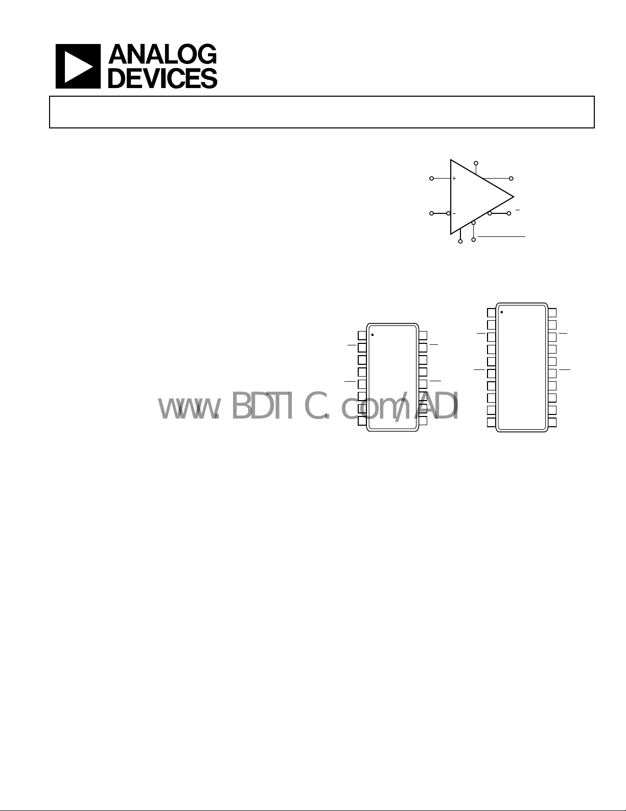
FUNCTIONAL BLOCK DIAGRAM
NONINVERTING
INPUT
INVERTING
INPUT
LATCH ENABLE
INPUT
1
QA
2
QA
3
V
DD
ADCMP561
4
LEA
LEA
V
–INA
+INA
EE
TOP VIEW
5
(Not to Scale)
6
7
8
Figure 2. ADCMP561 16-Lead QSOP Figure 3. ADCMP562 20-Lead QSOP
are fully compatible with PECL 10 K and 10 KH logic families.
The outputs provide sufficient drive current to directly drive
transmission lines terminated in 50 Ω to V
input, which is included, permits tracking, track-and-hold, or
sample-and-hold modes of operation. The latch input pins
contain internal pull-ups that set the latch in tracking mode
when left open.
16
QB
15
QB
14
GND
13
LEB
12
LEB
11
V
CC
10
–INB
+INB
9
HYS*
ADCMP561/
ADCMP562
LATCH ENABLE
INPUT
*ADCMP562 ONLY
Figure 1.
V
DD
QA
QA
V
DD
LEA
LEA
V
EE
–INA
+INA
HYS
04687-0-002
1
2
3
ADCMP562
4
TOP VIEW
5
(Not to Scale)
6
7
8
9
10
DD
Q OUTPUT
Q OUTPUT
04687-0-001
V
20
QB
19
QB
18
GND
17
LEB
16
LEB
15
V
14
–INB
13
+INB
12
HYSB
11
− 2 V. A latch
DD
CC
04687-0-003
A differential input stage permits consistent propagation delay
with a wide variety of signals in the common-mode range from
−2.0 V to +3.0 V. Outputs are complementary digital signals that
Rev. A
Information furnished by Analog Devices is believed to be accurate and reliable.
However, no responsibility is assumed by Analog Devices for its use, nor for any
infringements of patents or other rights of third parties that may result from its use.
Specifications subject to change without notice. No license is granted by implication
or otherwise under any patent or patent rights of Analog Devices. Trademarks and
registered trademarks are the property of their respective owners.
The ADCMP561/ADCMP562 are specified over the industrial
temperature range (−40°C to +85°C).
One Technology Way, P.O. Box 9106, Norwood, MA 02062-9106, U.S.A.
Tel: 781.329.4700 www.analog.com
Fax: 781.326.8703 © 2004 Analog Devices, Inc. All rights reserved.

ADCMP561/ADCMP562
www.BDTIC.com/ADI
TABLE OF CONTENTS
Specifications..................................................................................... 3
Absolute Maximum Ratings............................................................ 5
Thermal Considerations.............................................................. 5
ESD Caution.................................................................................. 5
Pin Configurations and Function Descriptions ........................... 6
Typical Performance Characteristics ............................................. 8
Timing Information ....................................................................... 10
Application Information................................................................ 11
REVISION HISTORY
7/04—Data Sheet Changed from Rev. 0 to Rev. A
Changes to Specification Table ....................................................... 4
Changes to Figure 14........................................................................ 9
Changes to Figure 21...................................................................... 12
Changes to Figure 23...................................................................... 13
4/04—Revision 0: Initial Version
Clock Timing Recovery............................................................. 11
Optimizing High Speed Performance ..................................... 11
Comparator Propagation Delay Dispersion ........................... 11
Comparator Hysteresis .............................................................. 12
Minimum Input Slew Rate Requirement ................................ 12
Typical Application Ci rcuits .......................................................... 13
Outline Dimensions....................................................................... 14
Ordering Guide .......................................................................... 14
Rev. A | Page 2 of 16
ADCMP561/ADCMP562
www.BDTIC.com/ADI
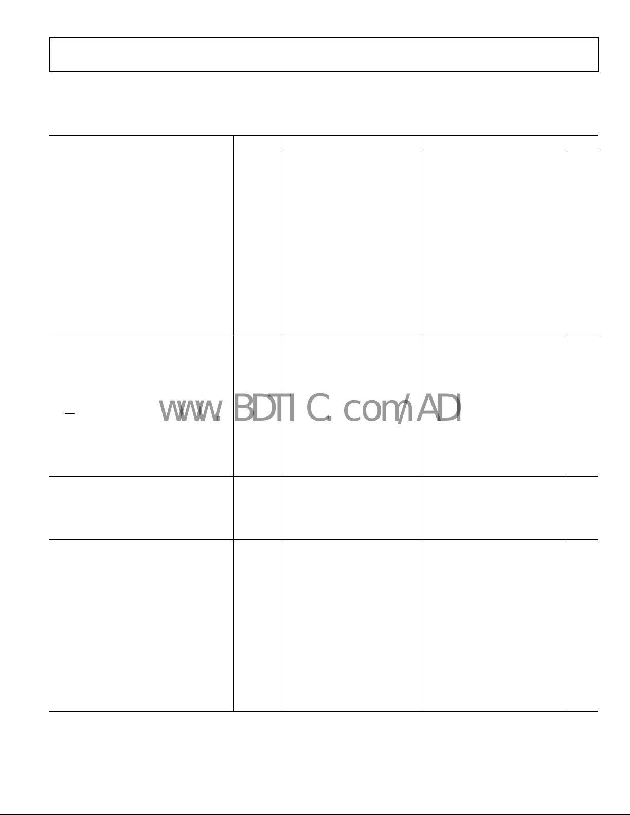
SPECIFICATIONS
VCC = +5.0 V, VEE = −5.2 V, VDD = +3.3 V, TA = −40°C to +85°C. Typical values are at TA = +25°C, unless otherwise noted.
Table 1. Electrical Characteristics
Parameter Symbol Conditions Min Typ Max Unit
DC INPUT CHARACTERISTICS
Input Voltage Range −2.0 3.0 V
Input Differential Voltage −5 +5 V
Input Offset Voltage V
OS
Input Offset Voltage Channel Matching ±2.0 mV
Offset Voltage Tempco ∆VOS/d
Input Bias Current I
IN
Input Bias Current Tempco 0.5 nA/°C
Input Offset Current ±1.0 µA
Input Capacitance C
IN
Input Resistance, Differential Mode 750 kΩ
Input Resistance, Common Mode 1800 kΩ
Active Gain A
V
Common-Mode Rejection Ratio CMRR VCM = −2.0 V to +3.0 V 80 dB
Hysteresis R
LATCH ENABLE CHARACTERISTICS
Latch Enable Voltage Range VDD − 2.0 V
Latch Enable Differential Voltage Range 0.4 2.0 V
Latch Enable Input High Current @ V
Latch Enable Input Low Current @ VDD −2.0 V −300 +300 µA
LE Voltage, Open Latch inputs not connected VDD − 0.2 V
LE Voltage, Open
Latch Setup Time t
Latch Hold Time t
Latch-to-Output Delay t
Latch Minimum Pulse Width t
Latch inputs not connected V
S
H
, t
PLOH
PL
DC OUTPUT CHARACTERISTICS
Output Voltage—High Level V
Output Voltage—Low Level V
Rise Time t
Fall Time t
OH
OL
R
F
AC PERFORMANCE
Propagation Delay t
PD
V
Propagation Delay Tempco ∆tPD /d
Prop Delay Skew—Rising Transition to
Falling Transition
Within Device Propagation Delay Skew—
Channel-to-Channel
Overdrive Dispersion 20 mV ≤ VOD ≤ 100 mV 75 ps
Overdrive Dispersion 100 mV ≤ VOD ≤ 1.5 V 75 ps
Slew Rate Dispersion 0.4 V/ns ≤ SR ≤ 1.33 V/ns 50 ps
Pulse Width Dispersion 700 ps ≤ PW ≤ 10 ns 25 ps
Duty Cycle Dispersion 33 MHz, 1 V/ns, 0.5 V 15 ps
Common-Mode Voltage Dispersion 1 V swing, −1.5 V ≤ VCM ≤ +2.5 V 10 ps
VCM = 0 V −10.0 ±2.0 +10.0 mV
2.0 µV/°C
T
−IN = −2 V, +IN = +3 V −10.0 ±3 +10.0 µA
0.75 pF
63 dB
= ∞ ±1.0 mV
HYS
DD
DD
−300 +300 µA
VDD + 0.1 V
DD
/2 − 0.2 VDD/2 VDD/2 + 0.2 V
DD
V
VOD = 250 mV 250 ps
VOD = 250 mV 250 ps
PLOLVOD
= 250 mV 600 ps
VOD = 250 mV 500 ps
PECL 50 Ω to VDD − 2.0 V VDD − 1.15 VDD − 0.81 V
PECL 50 Ω to VDD − 2.0 V VDD − 1.95 VDD − 1.54 V
10% to 90% 550 ps
10% to 90% 470 ps
VOD = 1 V 700 ps
= 20 mV 830 ps
OD
VOD = 1 V 0.25 ps/°C
T
= 1 V 50 ps
V
OD
V
= 1 V 50 ps
OD
Rev. A | Page 3 of 16
ADCMP561/ADCMP562
www.BDTIC.com/ADI
Parameter Symbol Conditions Min Typ Max Unit
AC PERFORMANCE (continued)
Equivalent Input Rise Time Bandwidth1 BW
EQ
Maximum Toggle Rate >50% output swing 800 MHz
Minimum Pulse Width PW
MIN
RMS Random Jitter
Unit-to-Unit Propagation Delay Skew 100 ps
POWER SUPPLY
Positive Supply Current I
Negative Supply Current I
Logic Supply Current I
VCC
VEE
VDD
Logic Supply Current @ 3.3 V with load 45 60 70 mA
Positive Supply Voltage V
Negative Supply Voltage V
Logic Supply Voltage V
Power Dissipation P
CC
EE
DD
D
Power Dissipation Dual, with load 180 220 250 mW
DC Power Supply Rejection Ratio—V
DC Power Supply Rejection Ratio—V
DC Power Supply Rejection Ratio—V
CC
EE
DD
PSRR
PSRR
PSRR
HYSTERESIS (ADCMP562 Only)
Hysteresis R
R
0 V to 1 V swing, 2 V/ns 1500 MHz
∆tPD < 25 ps 700 ps
= 400 mV, 1.3 V/ns, 312 MHz,
V
OD
1.0 ps
50% duty cycle
@ +5.0 V 2 3.2 5 mA
@ −5.2 V 10 22 28 mA
@ 3.3 V without load 6 9 13 mA
Dual 4.75 5.0 5.25 V
Dual −4.96 −5.2 −5.45 V
Dual 2.5 3.3 5.0 V
Dual, without load 130 160 190 mW
85 dB
VCC
85 dB
VEE
85 dB
VDD
= 19.5 kΩ 20 mV
HYS
= 8.0 kΩ 70 mV
HYS
1
Equivalent input rise time bandwidth assumes a first-order input response and is calculated by the following formula: BWEQ = 0.22/√ (tr
20/80 input transition time applied to the comparator and tr
is the effective transition time as digitized by the comparator input.
COMP
COMP
2
2
– tr
), where trIN is the
IN
Rev. A | Page 4 of 16
ADCMP561/ADCMP562
www.BDTIC.com/ADI
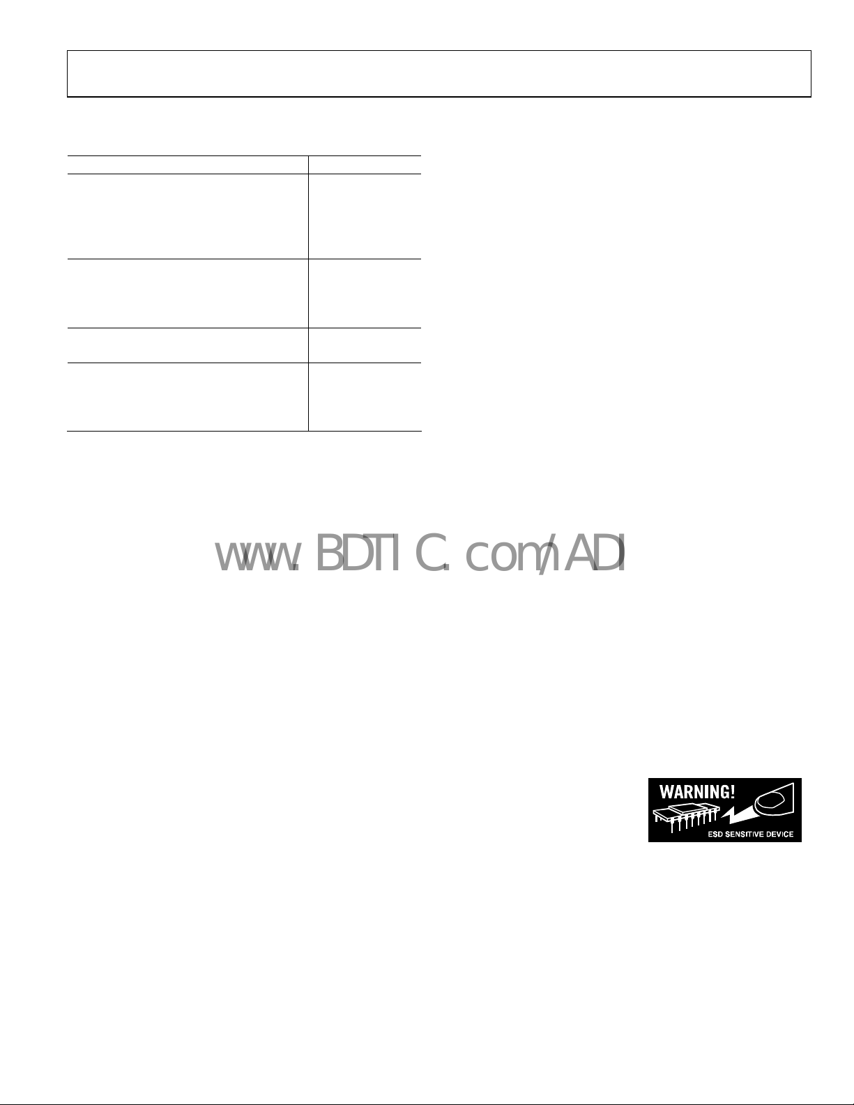
ABSOLUTE MAXIMUM RATINGS
Table 2.
Parameter Rating
Supply Voltages
Positive Supply Voltage (VCC to GND) −0.5 V to +6.0 V
Negative Supply Voltage (VEE to GND) −6.0 V to +0.5 V
Logic Supply Voltage (VDD to GND) −0.5 V to +6.0 V
Ground Voltage Differential −0.5 V to +0.5 V
Input Voltages
Input Common-Mode Voltage −3.0 V to +4.0 V
Differential Input Voltage −7.0 V to +7.0 V
Input Voltage, Latch Controls −0.5 V to +5.5 V
Output
Output Current 30 mA
Temperature
Operating Temperature, Ambient −40°C to +85°C
Operating Temperature, Junction 125°C
Storage Temperature Range −65°C to +150°C
Stresses above those listed under Absolute Maximum Ratings
may cause permanent damage to the device. This is a stress
rating only; functional operation of the device at these or any
other conditions above those indicated in the operational
sections of this specification is not implied. Exposure to
absolute maximum rating conditions for extended periods may
affect device reliability.
THERMAL CONSIDERATIONS
The ADCMP561 QSOP 16-lead package option has a θJA
(junction-to-ambient thermal resistance) of 104°C/W in
still air.
The ADCMP562 QSOP 20-lead package option has a θ
(junction-to-ambient thermal resistance) of 80°C/W in
still air.
JA
ESD CAUTION
ESD (electrostatic discharge) sensitive device. Electrostatic charges as high as 4000 V readily accumulate on
the human body and test equipment and can discharge without detection. Although this product features
proprietary ESD protection circuitry, permanent damage may occur on devices subjected to high energy
electrostatic discharges. Therefore, proper ESD precautions are recommended to avoid performance
degradation or loss of functionality.
Rev. A | Page 5 of 16

ADCMP561/ADCMP562
A
www.BDTIC.com/ADI
PIN CONFIGURATIONS AND FUNCTION DESCRIPTIONS
QA
QA
V
LEA
LEA
V
–INA
+INA
DD
EE
1
2
3
ADCMP561
4
TOP VIEW
5
(Not to Scale)
6
7
8
16
QB
15
QB
14
GND
13
LEB
12
LEB
11
V
CC
10
–INB
+INB
9
04687-0-002
Figure 4. ADCMP561 16-Lead QSOP Pin Configuration Figure 5. ADCMP562 20-Lead QSOP Pin Configuration
Table 3. Pin Function Descriptions
Pin No.
ADCMP561 ADCMP562 Mnemonic Function
1 V
DD
1 2 QA
Logic Supply Terminal.
One of two complementary outputs for Channel A. QA is logic high if the analog voltage at the
noninverting input is greater than the analog voltage at the inverting input (provided the
comparator is in compare mode). See the description of Pin LEA for more information.
2 3
QA
One of two complementary outputs for Channel A. QA is logic low if the analog voltage at the
noninverting input is greater than the analog voltage at the inverting input (provided the
comparator is in compare mode). See the description of Pin LEA for more information.
3 4 V
DD
4 5 LEA
Logic Supply Terminal.
One of two complementary inputs for Channel A Latch Enable. In compare mode (logic high),
the output tracks changes at the input of the comparator. In the latch mode (logic low), the
output reflects the input state just prior to the comparator’s being placed in the latch mode.
LEA must be driven in conjunction with LEA. If left unconnected, the comparator defaults to
compare mode.
5 6
LEA
One of two complementary inputs for Channel A Latch Enable. In compare mode (logic low),
the output tracks changes at the input of the comparator. In latch mode (logic high), the
output reflects the input state just prior to the comparator’s being placed in the latch mode.
LEA must be driven in conjunction with LEA. If left unconnected, the comparator defaults to
compare mode.
6 7 V
EE
7 8 −INA
Negative Supply Terminal.
Inverting Analog Input of the Differential Input Stage for Channel A. The inverting A input must
be driven in conjunction with the noninverting A input.
8 9 +INA
Noninverting Analog Input of the Differential Input Stage for Channel A. The noninverting
A input must be driven in conjunction with the inverting A input.
10 HYSA Programmable Hysteresis Input.
11 HYSB Programmable Hysteresis Input.
9 12 +INB
Noninverting Analog Input of the Differential Input Stage for Channel B. The noninverting
B input must be driven in conjunction with the inverting B input.
10 13 −INB
Inverting Analog Input of the Differential Input Stage for Channel B. The inverting B input must
be driven in conjunction with the noninverting B input.
11 14 V
12 15
CC
LEB
Positive Supply Terminal.
One of two complementary inputs for Channel B Latch Enable. In compare mode (logic low),
the output tracks changes at the input of the comparator. In latch mode (logic high), the
output reflects the input state just prior to placing the comparator in the latch mode. LEB
must be driven in conjunction with LEB
. If left unconnected, the comparator defaults to
compare mode.
13 16 LEB
One of two complementary inputs for Channel B Latch Enable. In compare mode (logic high),
the output tracks changes at the input of the comparator. In latch mode (logic low), the output
reflects the input state just prior to placing the comparator in the latch mode. LEB
driven in conjunction with LEB. If left unconnected, the comparator defaults to compare mode.
–INA
+INA
HYS
V
QA
QA
V
LEA
LEA
V
DD
DD
EE
1
2
3
ADCMP562
4
TOP VIEW
5
(Not to Scale)
6
7
8
9
10
V
20
DD
QB
19
QB
18
GND
17
LEB
16
LEB
15
V
14
CC
–INB
13
+INB
12
HYSB
11
04687-0-003
must be
Rev. A | Page 6 of 16

ADCMP561/ADCMP562
www.BDTIC.com/ADI
Pin No.
ADCMP561 ADCMP562 Mnemonic Function
14 17 GND Analog Ground.
15 18
16 19 QB
20 V
QB
DD
One of two complementary outputs for Channel B. QB is logic low if the analog voltage at the
noninverting input is greater than the analog voltage at the inverting input (provided the
comparator is in compare mode). See the description of PIN LEB for more information.
One of two complementary outputs for Channel B. QB is logic high if the analog voltage at the
noninverting input is greater than the analog v
comparator is in compare mode). See the description of Pin LEB for more information.
Logic Supply Terminal.
oltage at the inverting input (provided the
Rev. A | Page 7 of 16

ADCMP561/ADCMP562
www.BDTIC.com/ADI
TYPICAL PERFORMANCE CHARACTERISTICS
V
= +5.0 V, VEE = –5.2 V, VDD = +3.3 V, TA = 25°C, unless otherwise noted.
CC
3.0
2.5
2.0
1.5
1.0
0.5
0
INPUT BIAS CURRENT (µA)
–0.5
–1.0
–2.5 –1.5 –0.5 0.5 1.5 2.5 3.5
NONINVERTING INPUT VOLTAGE (INVERTING VOLTAGE = 0V)
Figure 6. Input Bias Current vs. Input Voltage
2.00
1.95
1.90
1.85
1.80
1.75
1.70
1.65
OFFSET VOLTAGE (mV)
1.60
1.55
1.50
–40–200 20406080
TEMPERATURE (°C)
Figure 7. Input Offset Voltage vs. Temperature
575
570
565
560
555
550
TIME (ps)
545
540
535
530
525
–40–30–20–100 102030405060708090
TEMPERATURE (°C)
Figure 8. Rise Time v s. Temperature
04687-0-013
04687-0-014
04687-0-015
2.80
2.78
2.76
2.74
2.72
2.70
2.68
(+IN = 3V, –IN = 0V)
2.66
2.64
+IN INPUT BIAS CURRENT (µA)
2.62
2.60
–40–200 20406080
TEMPERATURE (°C)
Figure 9. Input Bias Current vs. Temperature
2.6
2.4
2.2
2.0
1.8
OUTPUT RISE AND FALL (V)
1.6
1.4
0 0.25 0.50 0.75 1.00 1.25 1.50 1.75 2.00
TIME (ns)
Figure 10. Rise and Fall of Outputs vs. Time
500
495
490
485
480
475
TIME (ps)
470
465
460
455
450
–40–30–20–100 102030405060708090
TEMPERATURE (°C)
Figure 11. Fall Time vs. Temperature
04687-0-016
04687-0-017
04687-0-018
Rev. A | Page 8 of 16

ADCMP561/ADCMP562
www.BDTIC.com/ADI
715
708
710
705
700
695
690
PROPAGATION DELAY (ps)
685
680
–40–30–20–100 102030405060708090
TEMPERATURE (°C)
Figure 12. Propagation Delay vs. Temperature
140
120
100
80
60
40
04687-0-019
706
704
702
700
698
PROPAGATION DELAY (ps)
696
694
–2–10123
INPUT COMMON-MODE VOLTAGE (V)
Figure 15. Propagation Delay vs. Common-Mode Voltage
25
20
15
10
5
04687-0-022
PROPAGATION DELAY ERROR (ps)
20
0
0 1.61.41.21.00.80.60.40.2
OVERDRIVE VOLTAGE (V)
Figure 13. Propagation Delay vs. Overdrive Voltage
160
140
120
100
80
60
40
PROGRAMMED HYSTERESIS (mV)
20
0
R
(kΩ)
HYS
Figure 14. Comparator Hysteresis vs. R
04687-0-020
04687-0-021
01020304050
HYS
0
PROPAGATION DELAY ERROR (ps)
–5
0.7 1.7 2.7 3.7 4.7 5.7 6.7 7.7 8.7 9.7
PULSE WIDTH (ns)
Figure 16. Propagation Delay Error vs. Pulse Width
160
140
120
100
80
60
40
PROGRAMMED HYSTERESIS (mV)
20
0
0 50 100 150
Figure 17. Comparator Hysteresis vs. I
I
HYS
(µA)
HYS
04687-0-023
04687-0-024
Rev. A | Page 9 of 16

ADCMP561/ADCMP562
www.BDTIC.com/ADI
TIMING INFORMATION
LATCH ENABLE
LATCH ENABLE
DIFFERENTIAL
INPUT VOLTAGE
50%
t
S
t
H
V
IN
V
OD
t
PL
V
± V
REF
OS
Q OUTPUT
Q OUTPUT
t
t
PDL
PDH
t
F
t
R
t
PLOH
t
PLOL
50%
50%
04687-0-004
Figure 18. System Timing Diagram
Figure 18 shows the compare and latch features of the ADCMP561/ADCMP562. Table 4 describes the terms in the diagram.
Table 4. Timing Descriptions
Symbol Timing Description
t
PDH
Input to Output High Delay
Propagation delay measured from the time the input signal crosses the reference (± the
input offset voltage) to the 50% point of an output low-to-high transition.
t
PDL
Input to Output Low Delay
Propagation delay measured from the time the input signal crosses the reference (± the
input offset voltage) to the 50% point of an output high-to-low transition.
t
PLOH
Latch Enable to Output High Delay
Propagation delay measured from the 50% point of the latch enable signal low-to-high
transition to the 50% point of an output low-to-high transition.
t
PLOL
Latch Enable to Output Low Delay
Propagation delay measured from the 50% point of the latch enable signal low-to-high
transition to the 50% point of an output high-to-low transition.
t
H
Minimum Hold Time
Minimum time after the negative transition of the latch enable signal that the input signal
must remain unchanged to be acquired and held at the outputs.
t
PL
t
S
Minimum Latch Enable Pulse Width Minimum time the latch enable signal must be high to acquire an input signal change.
Minimum Setup Time
Minimum time before the negative transition of the latch enable signal that an input
signal change must be present to be acquired and held at the outputs.
t
R
Output Rise Time
Amount of time required to transition from a low to a high output as measured at the
20% and 80% points.
t
F
Output Fall Time
Amount of time required to transition from a high to a low output as measured at the
20% and 80% points.
V
OD
Voltage Overdrive Difference between the differential input and reference input voltages.
Rev. A | Page 10 of 16

ADCMP561/ADCMP562
www.BDTIC.com/ADI
APPLICATION INFORMATION
The ADCMP561/ADCMP562 comparators are very high speed
devices. Consequently, high speed design techniques must be
employed to achieve the best performance. The most critical
aspect of any ADCMP561/ADCMP562 design is the use of a
low impedance ground plane. A ground plane, as part of a
multilayer board, is recommended for proper high speed
performance. Using a continuous conductive plane over the
surface of the circuit board can create this, allowing breaks in
the plane only for necessary signal paths. The ground plane
provides a low inductance ground, eliminating any potential
differences at different ground points throughout the circuit
board caused by ground bounce. A proper ground plane also
minimizes the effects of stray capacitance on the circuit board.
It is also important to provide bypass capacitors for the power
su
pply in a high speed application. A 1 µF electrolytic bypass
capacitor should be placed within 0.5 inches of each power
supply pin to ground. These capacitors reduce any potential
voltage ripples from the power supply. In addition, a 10 nF
ceramic capacitor should be placed as close as possible from the
power supply pins on the ADCMP561/ADCMP562 to ground.
These capacitors act as a charge reservoir for the device during
high frequency switching.
The LATCH ENABLE input is active low (latched). If the
l
atching function is not used, the LATCH ENABLE input may
be left open or may be attached to V
high). The complementary input,
open or may be tied to V
unconnected or providing the proper voltages disables the
latching function.
Occasionally, one of the two comparator stages within the
AD
CMP561/ADCMP562 is not used. The inputs of the unused
comparator should not be allowed to float. The high internal
gain may cause the output to oscillate (possibly affecting the
comparator that is being used) unless the output is forced into a
fixed state. This is easily accomplished by ensuring that the two
inputs are at least one diode drop apart, while also appropriately
connecting the LATCH ENABLE and
as described previously.
The best performance is achieved with the use of proper PECL
erminations. The open emitter outputs of the ADCMP561/
t
ADCMP562 are designed to be terminated through 50 Ω
resistors to V
ation. If high speed PECL signals must be routed more than a
centimeter, microstrip or stripline techniques may be required
to ensure proper transition times and prevent output ringing.
− 2.0 V, or any other equivalent PECL termin-
DD
− 2.0 V. Leaving the latch inputs
DD
(VDD is a PECL logic
DD
LATCH ENABLE
LATCH ENABLE
, may b e left
inputs
CLOCK TIMING RECOVERY
Comparators are often used in digital systems to recover clock
timing signals. High speed square waves transmitted over a
distance, even tens of centimeters, can become distorted due to
stray capacitance and inductance. Poor layout or improper
termination can also cause reflections on the transmission line,
further distorting the signal waveform. A high speed
comparator can be used to recover the distorted waveform
while maintaining a minimum of delay.
OPTIMIZING HIGH SPEED PERFORMANCE
As with any high speed comparator amplifier, proper design and
layout techniques should be used to ensure optimal performance from the ADCMP561/ADCMP562. The performance
limits of high speed circuitry can be a result of stray capacitance, improper ground impedance, or other layout issues.
Minimizing resistance from source to the input is an important
co
nsideration in maximizing the high speed operation of the
ADCMP561/ADCMP562. Source resistance in combination
with equivalent input capacitance could cause a lagged response
at the input, thus delaying the output. The input capacitance of
the ADCMP561/ADCMP562, in combination with stray
capacitance from an input pin to ground, could result in several
picofarads of equivalent capacitance. A combination of 3 kΩ
source resistance and 5 pF of input capacitance yields a time
constant of 15 ns, which is significantly slower than the 750 ps
capability of the ADCMP561/ADCMP562. Source impedances
should be significantly less than 100 Ω for best performance.
Sockets should be avoided due to stray capacitance and induct
ance. If proper high speed techniques are used, the devices
should be free from oscillation when the comparator input
signal passes through the switching threshold.
COMPARATOR PROPAGATION DELAY DISPERSION
The ADCMP561/ADCMP562 have been specifically designed
to reduce propagation delay dispersion over an input overdrive
range of 100 mV to 1.5 V. Propagation delay overdrive
dispersion is the change in propagation delay that results from a
change in the degree of overdrive (how far the switching point
is exceeded by the input). The overall result is a higher degree of
timing accuracy because the ADCMP561/ADCMP562 are far
less sensitive to input variations than most comparator designs.
Rev. A | Page 11 of 16

ADCMP561/ADCMP562
www.BDTIC.com/ADI
Propagation delay dispersion is a specification that is important
in critical timing applications such as ATE, bench instruments,
and nuclear instrumentation. Overdrive dispersion is defined
as the variation in propagation delay as the input overdrive
conditions are changed (Figure 19). For the ADCMP561 and
ADCMP562, overdrive dispersion is typically 75 ps as the
overdrive is changed from 100 mV to 1.5 V. This specification
applies for both positive and negative overdrive because the
ADCMP561/ADCMP562 have equal delays for positive and
negative going inputs.
1.5V OVERDRIVE
INPUT VOLTAGE
20mV OVERDRIVE
± V
V
REF
OS
hysteresis versus resistance curve is shown in Figure 21.
A current source can also be used with the HYS pin. The
relationship between the current applied to the HYS pin and the
resulting hysteresis is shown in Figure 17.
–V
H
2
0
0V
+V
H
2
INPUT
1
DISPERSION
Q OUTPUT
Figure 19. Propagation Delay Dispersion
04687-0-005
COMPARATOR HYSTERESIS
The addition of hysteresis to a comparator is often useful in a
noisy environment, or where it is not desirable for the
comparator to toggle between states when the input signal is at
the switching threshold. The transfer function for a comparator
with hysteresis is shown in Figure 20. If the input voltage
approaches the threshold from the negative direction, the
comparator switches from a 0 to a 1 when the input crosses
+V
/2. The new switching threshold becomes −VH/2. The
H
comparator remains in a 1 state until the threshold −V
crossed, coming from the positive direction. In this manner,
noise centered on 0 V input does not cause the comparator to
switch states unless it exceeds the region bounded by ±V
Positive feedback from the output to the input is often used to
produce hysteresis in a comparator (Figure 24). The major
problem with this approach is that the amount of hysteresis
varies with the output logic levels, resulting in a hysteresis that
is not symmetrical around zero.
In the ADCMP562, hysteresis is generated through the
programmable hysteresis pin. A resistor from the HYS pin to
GND creates a current into the part that is used to generate
hysteresis. Hysteresis generated in this manner is independent
of output swing and is symmetrical around the trip point. The
/2 is
H
/2.
H
OUTPUT
04687-0-006
Figure 20. Comparator Hysteresis Transfer Function
160
140
120
100
80
60
40
PROGRAMMED HYSTERESIS (mV)
20
0
R
HYS
Figure 21. Comparator Hysteresis vs. R
(kΩ)
HYS
01020304050
04687-0-021
MINIMUM INPUT SLEW RATE REQUIREMENT
As for all high speed comparators, a minimum slew rate must
be met to ensure that the device does not oscillate when the
input crosses the threshold. This oscillation is due in part to the
high input bandwidth of the comparator and the parasitics of
the package. Analog Devices recommends a slew rate of 1 V/µs
or faster to ensure a clean output transition. If slew rates less
than 1 V/µs are used, hysteresis should be added to reduce the
oscillation.
Rev. A | Page 12 of 16

ADCMP561/ADCMP562
A
www.BDTIC.com/ADI
TYPICAL APPLICATION CIRCUITS
V
IN
V
REF
ADCMP561/
ADCMP562
LATCH
ENABLE
INPUTS
ALL RESISTORS 50Ω
– 2V
V
DD
Figure 22. High Speed Sampling Circuits
+V
REF
V
IN
–V
REF
LL RESISTORS 50Ω UNLESS OTHERWISE NOTED
ADCMP561/
ADCMP562
ADCMP561/
ADCMP562
LATCH
ENABLE
INPUTS
VDD–2V
VDD–2V
Figure 23. High Speed Window Comparator
OUTPUTS
OUTPUTS
OUTPUTS
04687-0-008
04687-0-009
V
IN
V
REF
ALL RESISTORS 50Ω, UNLESS OTHERWISE NOTED
ADCMP562
HYS
0Ω TO 80kΩ
VDD– 2.0V
OUTPUTS
Figure 24. Adding Hysteresis Using the HYS Control Pin
50Ω
V
IN
ADCMP561/
ADCMP562
50Ω
100Ω100Ω
(VDD– 2V)× 2
Figure 25. How to Interface a PECL Output to an
Instrument with a 50 Ω to Ground Input
50Ω
50Ω
04687-0-010
04687-0-012
Rev. A | Page 13 of 16

ADCMP561/ADCMP562
C
Y
www.BDTIC.com/ADI
OUTLINE DIMENSIONS
0.065
0.049
0.010
0.004
COPLANARITY
0.004
Figure 26. 16-Lead Shrink Small Outline Package [QSOP]
PIN 1
0.193
BSC
0.012
0.008
9
8
0.154
BSC
0.069
0.053
SEATING
PLANE
0.236
BSC
0.010
0.006
16
1
PIN 1
0.025
BSC
COMPLIANT TO JEDEC STANDARDS MO-137AB
(RQ-16)
Dimensions shown in inches
0.341
BSC
20 11
1
0.154
BSC
10
0.236
BSC
8°
0°
0.050
0.016
0.010
0.004
OPLANARIT
0.004
0.065
0.049
0.025
BSC
COMPLIANT TO JEDEC STANDARDS MO-137AD
0.012
0.008
0.069
0.053
SEATING
PLANE
0.010
0.006
8°
0°
0.050
0.016
Figure 27. 20-Lead Shrink Small Outline Package [QSOP]
(RQ-20)
Dimensions shown in inches
ORDERING GUIDE
Model Temperature Range Package Description Package Option
ADCMP561BRQ −40°C to +85°C 16-Lead QSOP RQ-16
ADCMP562BRQ −40°C to +85°C 20-Lead QSOP RQ-20
Rev. A | Page 14 of 16

ADCMP561/ADCMP562
www.BDTIC.com/ADI
NOTES
Rev. A | Page 15 of 16

ADCMP561/ADCMP562
www.BDTIC.com/ADI
NOTES
© 2004 Analog Devices, Inc. All rights reserved. Trademarks and
registered trademarks are the property of their respective owners.
D04687–0–7/04(A)
Rev. A | Page 16 of 16
 Loading...