

查询ADCMP350YKS-REEL7供应商
Comparators and Reference Circuits
ADCMP350/ADCMP352/ADCMP354/ADCMP356
FEATURES
Comparators with 0.6 V on-chip references
Output stages:
Open-drain active-low (ADCMP350)
Push-pull active-low (ADCMP352)
Open-drain active-high (ADCMP354)
Push-pull active-high (ADCMP356)
High voltage (up to 22 V) tolerance on V
and open-drain
IN
output pins
Low power consumption (10 µA)
10 nA input bias current
15 mV hysteresis
5 µs propagation delay
Specified over −40°C to +125°C temperature range
4-lead SC70 package
APPLICATIONS
Voltage detectors
Microprocessor systems
Computers
Battery monitors
Intelligent instruments
Portable equipment
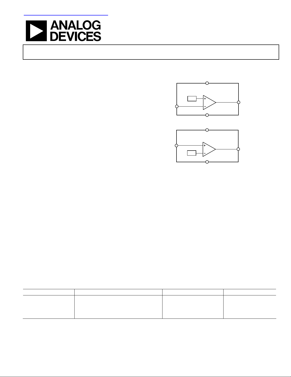
FUNCTIONAL BLOCK DIAGRAMS
ADCMP350/ADCMP352
REF
V
IN
ADCMP354/ADCMP356
V
IN
REF
V
GND
V
GND
CC
CC
Figure 1.
OUT (OD/PP)
OUT (OD/PP)
04745-001
`
GENERAL DESCRIPTION
The ADCMP350/ADCMP352/ADCMP354/ADCMP356 parts
are comparator and reference circuits suitable for use in
general-purpose applications. The high voltage input and
output structures will allow voltages of up to 22 V on the input
of all devices and the output of the open-drain devices. High
performance over the −40°C to +125°C temperature range
makes them suitable for use in automotive and other thermally
harsh applications, while low power consumption and spaceefficient SC70 packaging make them ideal for battery-powered
portable equipment.
Table 1. Selection Table
Part No. Reference Voltage (V) Input Connection Output
ADCMP350 0.6 Inverting Open Drain
ADCMP352 0.6 Inverting Push-Pull
ADCMP354 0.6 Noninverting Open Drain
ADCMP356 0.6 Noninverting Push-Pull
Rev. 0
Information furnished by Analog Devices is believed to be accurate and reliable.
However, no responsibility is assumed by Analog Devices for its use, nor for any
infringements of patents or other rights of third parties that may result from its use.
Specifications subject to change without notice. No license is granted by implication
or otherwise under any patent or patent rights of Analog Devices. Trademarks and
registered trademarks are the property of their respective owners.
One Technology Way, P.O. Box 9106, Norwood, MA 02062-9106, U.S.A.
Tel: 781.329.4700
Fax: 781.326.8703 © 2004 Analog Devices, Inc. All rights reserved.
www.analog.com

ADCMP350/ADCMP352/ADCMP354/ADCMP356
TABLE OF CONTENTS
Specifications..................................................................................... 3
Applications........................................................................................9
Absolute Maximum Ratings............................................................ 4
ESD Caution.................................................................................. 4
Pin Configuration and Function Descriptions............................. 5
Typical Performance Characteristics ............................................. 6
REVISION HISTORY
10/04—Revision 0: Initial Version
Adding Hysteresis..........................................................................9
Volt a ge D e te c tor ............................................................................9
Outline Dimensions ....................................................................... 10
Ordering Guide .......................................................................... 10
Rev. 0 | Page 2 of 12

ADCMP350/ADCMP352/ADCMP354/ADCMP356
SPECIFICATIONS
VCC = Full operating range, TA = –40°C to +125°C, unless otherwise noted.
Table 2.
Parameter Min Typ Max Unit Test Conditions/Comments
SUPPLY
VCC Operating Voltage Range 2.25 5.5 V
VIN Operating Voltage Range 0 22 V
Supply Current 10 15 µA
VIN THRESHOLD RISING 0.579 0.6 0.621 V VCC = 3.3V, TA = −40°C to +85°C
0.579 0.6 0.624 V VCC = 3.3V, TA = −40°C to +125°C
VIN THRESHOLD FALLING 0.564 0.585 0.606 V VCC = 3.3V, TA = −40°C to +85°C
0.564 0.585 0.609 V VCC = 3.3V, TA = −40°C to +125°C
INPUT BIAS CURRENT 10 nA VIN = 0.6 V
170 µA VIN = 22 V
THRESHOLD TEMPERATURE COEFFICIENT 30 ppm/°C
VIN TO OUT DELAY 5 µs VIN = VTH to (VTH − 100 mV)
OUT VOLTAGE LOW 0.4 V VIN < VTH min, I
OUT VOLTAGE HIGH 0.8 × V
OUTPUT RISE TIME 30 ns Cout = 15 pF
OUTPUT FALL TIME 45 ns Cout = 15 pF
OUTPUT LEAKAGE CURRENT 1 µA OUT = 22 V, open drain only
V
CC
> VTH max, I
V
IN
Push-pull only
= 1.2 mA
SINK
SOURCE
= 500 µA,
Rev. 0 | Page 3 of 12

ADCMP350/ADCMP352/ADCMP354/ADCMP356
ABSOLUTE MAXIMUM RATINGS
TA = 25°C, unless otherwise noted.
Table 3.
Parameter Rating
V
CC
V
IN
OUT (Open Drain) −0.3 V to +25 V
OUT (Push-Pull) −0.3 V to (VCC + 0.3 V)
Operating Temperature Range −40°C to +125°C
Storage Temperature Range −65°C to +150°C
θJA Thermal Impedance, SC70 146°C/W
Lead Temperature
Soldering (10 sec) 300°C
Vapor Phase (60 sec) 215°C
Infrared (15 sec) 220°C
−0.3 V to +6 V
−0.3 V to +25 V
Stresses above those listed under Absolute Maximum Ratings
may cause permanent damage to the device. This is a stress
rating only and functional operation of the device at these or
any other conditions above those indicated in the operational
section of this specification is not implied. Exposure to absolute
maximum rating conditions for extended periods may affect
device reliability.
ESD CAUTION
ESD (electrostatic discharge) sensitive device. Electrostatic charges as high as 4000 V readily accumulate on the
human body and test equipment and can discharge without detection. Although this product features
proprietary ESD protection circuitry, permanent damage may occur on devices subjected to high energy
electrostatic discharges. Therefore, proper ESD precautions are recommended to avoid performance
degradation or loss of functionality.
Rev. 0 | Page 4 of 12

ADCMP350/ADCMP352/ADCMP354/ADCMP356
G
PIN CONFIGURATION AND FUNCTION DESCRIPTIONS
V
1
IN
ADCMP350/
ADCMP352/
ADCMP354/
ADCMP356
ND OUT
Figure 2. Pin Configuration
4
V
CC
32
04745-002
Table 4. Pin Function Descriptions
Pin No. Mnemonic Description
1 V
IN
Monitors Analog Input Voltage. Connected to inverting or noninverting input, depending on model number.
2 GND Ground.
3 OUT Digital Output. Open-drain or push-pull options, depending on model number.
4 V
CC
Power Supply.
Rev. 0 | Page 5 of 12

ADCMP350/ADCMP352/ADCMP354/ADCMP356
TYPICAL PERFORMANCE CHARACTERISTICS
11.0
10.5
TA +25°C
10.0
TA+125°C
9.5
9.0
(µA)
CC
I
8.5
8.0
7.5
7.0
2.25 2.55 2.85 3.15 3.45 5.55
TA+85°C
TA–40°C
3.75 4.05 4.35 4.65 4.95 5.25
V
(V)
CC
Figure 3. ICC vs. VCC over Temperature.
05112-003
20
18
16
14
A)
µ
12
10
8
6
SUPPLY CURRENT (
4
2
0
02468 22
10 12 14 16 18 20
V
(V)
IN
Figure 6. Supply Current vs. Input Voltage
05112-006
700
680
660
640
620
V
TRIP RISING
TRIP
600
(mV)
TRIP
V
V
580
560
540
520
500
–40 –25 –10 5 20 35 50 65 80 95 110 125
TRIP FALLING
TRIP
TEMPERATURE (°C)
Figure 4. VIN Trip Threshold vs. Temperature.(VCC = 3.3V)
20
18
16
HYSTERESIS
14
12
10
8
HYSTERESIS (mV)
6
4
2
0
–40 –25 –10 5 20 35 50 65 80 95 110 125
TEMPERATURE (°C)
Figure 5. VIN Trip Hysteresis vs. Temperature
05112-004
05112-005
200
180
160
140
120
100
80
IN LEAKAGE (µA)
60
40
20
0
02468 22
T
TA = +125°C
10 12 14 16 18 20
(V)
V
IN
= +85°C
A
= +25°C
T
A
T
= –40°C
A
Figure 7. Input Leakage vs. Input Voltage
1.0
0.9
0.8
0.7
0.6
0.5
0.4
LEAKAGE (µA)
IN
V
0.3
0.2
0.1
0
0 0.3 0.6 0.9 1.2 1.5 1.8 2.1 2.4 2.7 3.0 3.3
Figure 8. V
Leakage Current vs. VIN Voltag e (VCC = 3.8 V)
IN
(V)
V
IN
TA = 25°C
05112-007
05112-019
Rev. 0 | Page 6 of 12

ADCMP350/ADCMP352/ADCMP354/ADCMP356
200
190
180
170
160
150
140
IN LEAKAGE (µA)
130
120
110
100
2.25 2.55 2.85 3.15 3.45 5.55
TA = +125°C
T
= +85°C
A
TA = +25°C
T
= –40°C
A
3.75 4.05 4.35 4.65 4.95 5.25
V
(V)
CC
Figure 9. Input Leakage vs. Supply Voltage (VIN = 22 V)
700
680
660
640
(mV)
TRIP
V
620
600
580
560
540
520
500
V
RISING
TRIP
V
FALLING
TRIP
2.25 2.55 2.85 3.15 3.45 5.55
3.75 4.05 4.35 4.65 4.95 5.25
V
(V)
CC
Figure 10. VIN Trip T hres hold vs. VCC
05112-009
05112-008
10000
T
= +25°C
A
1000
T
= +85°C
100
TA = +125°C
10
OUTPUT VOLTAGE (mV)
1
0.1
0.01 0.1 10
A
T
= –40°C
A
OUTPUT SINK CURRENT (mA)
1
Figure 12. Output Voltage vs. Output Sink Current (Isink = 500 mA)
120
100
80
60
40
OUTPUT LOW VOLTAGE (mV)
20
0
2.25 2.40 2.70 3.00 3.30 5.50
3.60 3.90 4.20 4.50 4.80 5.20
SUPPLY VOLTAGE (V)
Figure 13. Output Low Voltage vs. Supply Voltage (Isink = 500 mA)
05112-010
05112-011
20
18
16
14
12
10
8
HYSTERESIS (mV)
6
4
2
0
2.25 2.55 2.85 3.15 3.45 5.55
Figure 11. V
HYSTERESIS
3.75 4.05 4.35 4.65 4.95 5.25
V
(V)
CC
Trip Hysteresis vs. VCC
IN
05112-020
Rev. 0 | Page 7 of 12
200
180
160
140
120
100
80
FALL TIME (ns)
60
40
20
0
2.25 2.40 2.70 3.00 3.30 5.50
3.60 3.90 4.20 4.50 4.80 5.20
SUPPLY VOLTAGE (V)
RISE TIME
FALL TIME
Figure 14. Fall Time vs. Supply Voltage
05112-012

ADCMP350/ADCMP352/ADCMP354/ADCMP356
100
90
80
70
60
50
40
30
20
SHORT-CIRCUIT SINK CURRENT (mA)
10
0
2.25 2.40 2.70 3.00 3.30 5.50
Figure 15. Short-Circuit Sink Current vs. Supply Voltage
(V
25
3.60 3.90 4.20 4.50 4.80 5.20
SUPPLY VOLTAGE (V)
= 3.3, PUSH-PULL Only)
cc
05112-013
1
CH1 = VIN
CH2 = VOUT
2
CH1 20mV/DIV CH2 1.00V/DIV TIMEBASE: 10µs/DIV
Figure 17. Propagation Delay Timing, 10 mV Overdrive
05112-015
20
s)
µ
15
10
PROPAGATION DELAY (
5
0
t
PLH
t
PHL
10 80 90 100 110 130
INPUT OVERDRIVE (mV)
120706050403020
05112-014
Figure 16. Propagation Delay vs. Input Overdrive ( Vcc = 3.3, PUSH-PULL Only)
CH1 = VIN
1
CH2 = VOUT
2
CH1 100mV/DIV CH2 1.00V/DIV TIMEBASE: 10µs/DIV
Figure 18. Propagation Delay Timing, 100 mV Overdrive
05112-016
Rev. 0 | Page 8 of 12

ADCMP350/ADCMP352/ADCMP354/ADCMP356
(
APPLICATIONS
ADDING HYSTERESIS
To prevent oscillations at the output caused by noise or slowly
moving signals passing the switching threshold, positive
feedback can be used to add hysteresis to the noninverting parts
(ADCMP354 and ADCMP356).
For the noninverting configuration shown in Figure 19, two
resistors are used to create different switching thresholds,
depending on whether the input signal is increasing or
decreasing in magnitude. When the input voltage is increasing,
the threshold is above V
threshold is below V
The upper input threshold level is given by
V
IN_HI
where V
= 0.6 V.
REF
The lower input threshold level is given by
, and when it’s decreasing, the
REF
.
REF
V
=
IN_LO
()
REF
REF
=
R2
R2
−+
+
R2R1V
R1VR2R1V
CC
)
VOLTAGE DETECTOR
The ADCMP35x parts can be used to monitor voltages, such as
battery monitoring or threshold detectors. Using a resistor
divider at the input to select the appropriate trip voltage, the
comparator can be configured to give a logic output when the
input passes that threshold. Figure 20 shows the typical
configuration of the ADCMP354 for monitoring a supply to
indicate that the voltage is above a certain level.
V
= 5V
CC
ADM331
ADCMP354
V
IN
R1
R1
V
= 0.6V
REF
V
IN
Figure 20. Voltage Detector Application
OUT
R
PULLUP
05112-018
The hysteresis is the difference between these voltage levels and
is given by
R1V
CC
V
=∆
IN
R2
V
= 5V
CC
ADM331
ADCMP354
V
= 0.6V
REF
V
V
IN
IN
R1
R2
Figure 19. Noninverting Comparator Configuration with Hysteresis
OUT
R
PULLUP
R
LOAD
05112-017
Rev. 0 | Page 9 of 12

ADCMP350/ADCMP352/ADCMP354/ADCMP356
OUTLINE DIMENSIONS
2.20
1.35
1.15
PIN 1
0.65 BSC
1.80
4
1
3
2
*
0.50 BSC
2.40
1.80
0.70
0.50
1.10
0.80
SEATING
PLANE
0.18
0.10
0.30
0.10
1.00
0.80
0.10 MAX
0.30
0.15
0.10 COPLANARITY
*
PACKAGE OUTLINE CORRESPONDS IN FULL TO EIAJ SC82
EXCEPT FOR WIDTH OF PIN-2 AS SHOWN
Figure 21. 4-Lead Thin Shrink Small Outline Transistor Package [SC70]
(EIAJ SC82 body)
(KS-4)
Dimensions shown in millimeters
ORDERING GUIDE
Model Temperature Range Package Description Branding Package Option
ADCMP350YKS-REEL7 –40°C to +125°C 4-Lead SC70 M0Z KS-4
ADCMP352YKS-REEL7 –40°C to +125°C 4-Lead SC70 M11 KS-4
ADCMP354YKS-REEL7 –40°C to +125°C 4-Lead SC70 M13 KS-4
ADCMP356YKS-REEL7 –40°C to +125°C 4-Lead SC70 M15 KS-4
Rev. 0 | Page 10 of 12

ADCMP350/ADCMP352/ADCMP354/ADCMP356
NOTES
Rev. 0 | Page 11 of 12

ADCMP350/ADCMP352/ADCMP354/ADCMP356
NOTES
© 2004 Analog Devices, Inc. All rights reserved. Trademarks and
registered trademarks are the property of their respective owners.
D05112-0-10/04(0)
Rev. 0 | Page 12 of 12
 Loading...