Analog Devices ADCMP350 2 4 6 Datasheet

Comparators and Reference Circuits
ADCMP350/ADCMP352/ADCMP354/ADCMP356
FEATURES
Comparators with 0.6 V on-chip references
Output stages:
Open-drain active-low (ADCMP350)
Push-pull active-low (ADCMP352)
Open-drain active-high (ADCMP354)
Push-pull active-high (ADCMP356)
High voltage (up to 22 V) tolerance on V
and open-drain
IN
output pins
Low power consumption (10 µA)
10 nA input bias current
15 mV hysteresis
5 µs propagation delay
Specified over −40°C to +125°C temperature range
4-lead SC70 package
APPLICATIONS
Voltage detectors
Microprocessor systems
Computers
Battery monitors
Intelligent instruments
Portable equipment
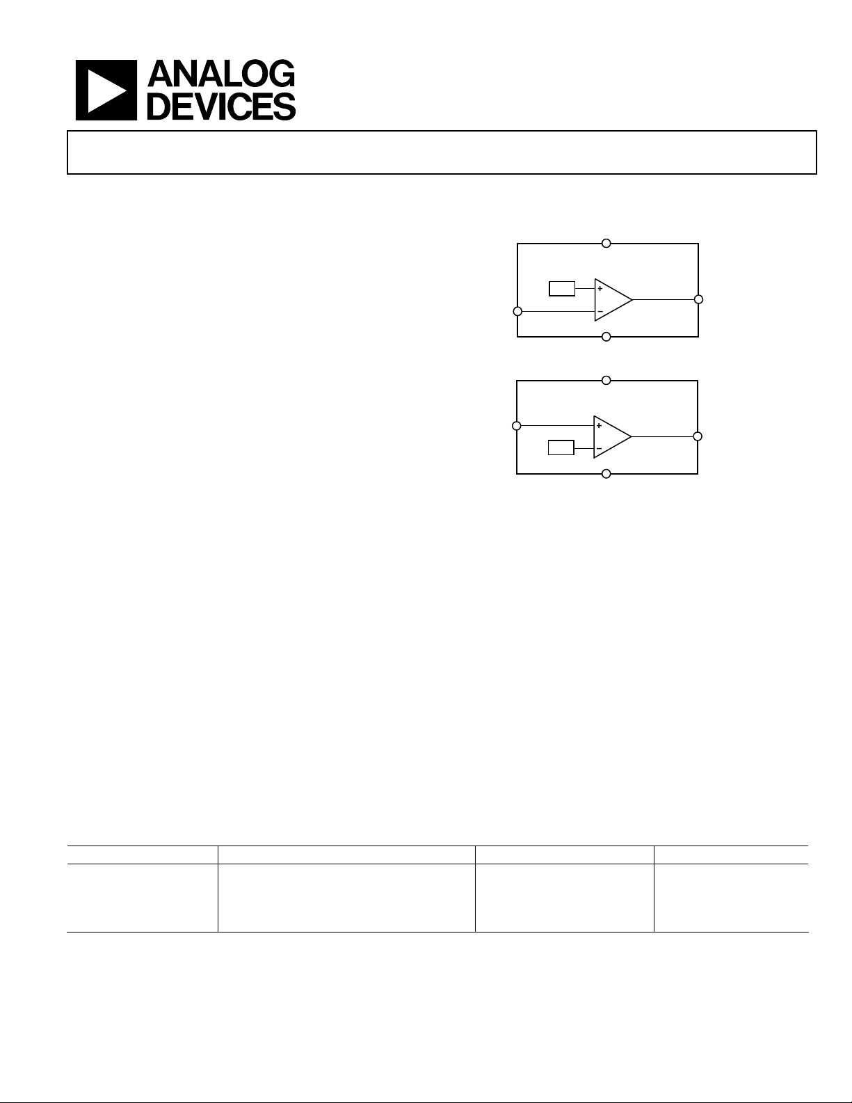
FUNCTIONAL BLOCK DIAGRAMS
ADCMP350/ADCMP352
REF
V
IN
ADCMP354/ADCMP356
V
IN
REF
V
GND
V
GND
CC
CC
Figure 1.
OUT (OD/PP)
OUT (OD/PP)
04745-001
`
GENERAL DESCRIPTION
The ADCMP350/ADCMP352/ADCMP354/ADCMP356 parts
are comparator and reference circuits suitable for use in
general-purpose applications. The high voltage input and
output structures will allow voltages of up to 22 V on the input
of all devices and the output of the open-drain devices. High
performance over the −40°C to +125°C temperature range
makes them suitable for use in automotive and other thermally
harsh applications, while low power consumption and spaceefficient SC70 packaging make them ideal for battery-powered
portable equipment.
Table 1. Selection Table
Part No. Reference Voltage (V) Input Connection Output
ADCMP350 0.6 Inverting Open Drain
ADCMP352 0.6 Inverting Push-Pull
ADCMP354 0.6 Noninverting Open Drain
ADCMP356 0.6 Noninverting Push-Pull
Rev. 0
Information furnished by Analog Devices is believed to be accurate and reliable.
However, no responsibility is assumed by Analog Devices for its use, nor for any
infringements of patents or other rights of third parties that may result from its use.
Specifications subject to change without notice. No license is granted by implication
or otherwise under any patent or patent rights of Analog Devices. Trademarks and
registered trademarks are the property of their respective owners.
One Technology Way, P.O. Box 9106, Norwood, MA 02062-9106, U.S.A.
Tel: 781.329.4700
Fax: 781.326.8703 © 2004 Analog Devices, Inc. All rights reserved.
www.analog.com

ADCMP350/ADCMP352/ADCMP354/ADCMP356
TABLE OF CONTENTS
Specifications..................................................................................... 3
Applications........................................................................................9
Absolute Maximum Ratings............................................................ 4
ESD Caution.................................................................................. 4
Pin Configuration and Function Descriptions............................. 5
Typical Performance Characteristics ............................................. 6
REVISION HISTORY
10/04—Revision 0: Initial Version
Adding Hysteresis..........................................................................9
Volt a ge D e te c tor ............................................................................9
Outline Dimensions ....................................................................... 10
Ordering Guide .......................................................................... 10
Rev. 0 | Page 2 of 12

ADCMP350/ADCMP352/ADCMP354/ADCMP356
SPECIFICATIONS
VCC = Full operating range, TA = –40°C to +125°C, unless otherwise noted.
Table 2.
Parameter Min Typ Max Unit Test Conditions/Comments
SUPPLY
VCC Operating Voltage Range 2.25 5.5 V
VIN Operating Voltage Range 0 22 V
Supply Current 10 15 µA
VIN THRESHOLD RISING 0.579 0.6 0.621 V VCC = 3.3V, TA = −40°C to +85°C
0.579 0.6 0.624 V VCC = 3.3V, TA = −40°C to +125°C
VIN THRESHOLD FALLING 0.564 0.585 0.606 V VCC = 3.3V, TA = −40°C to +85°C
0.564 0.585 0.609 V VCC = 3.3V, TA = −40°C to +125°C
INPUT BIAS CURRENT 10 nA VIN = 0.6 V
170 µA VIN = 22 V
THRESHOLD TEMPERATURE COEFFICIENT 30 ppm/°C
VIN TO OUT DELAY 5 µs VIN = VTH to (VTH − 100 mV)
OUT VOLTAGE LOW 0.4 V VIN < VTH min, I
OUT VOLTAGE HIGH 0.8 × V
OUTPUT RISE TIME 30 ns Cout = 15 pF
OUTPUT FALL TIME 45 ns Cout = 15 pF
OUTPUT LEAKAGE CURRENT 1 µA OUT = 22 V, open drain only
V
CC
> VTH max, I
V
IN
Push-pull only
= 1.2 mA
SINK
SOURCE
= 500 µA,
Rev. 0 | Page 3 of 12

ADCMP350/ADCMP352/ADCMP354/ADCMP356
ABSOLUTE MAXIMUM RATINGS
TA = 25°C, unless otherwise noted.
Table 3.
Parameter Rating
V
CC
V
IN
OUT (Open Drain) −0.3 V to +25 V
OUT (Push-Pull) −0.3 V to (VCC + 0.3 V)
Operating Temperature Range −40°C to +125°C
Storage Temperature Range −65°C to +150°C
θJA Thermal Impedance, SC70 146°C/W
Lead Temperature
Soldering (10 sec) 300°C
Vapor Phase (60 sec) 215°C
Infrared (15 sec) 220°C
−0.3 V to +6 V
−0.3 V to +25 V
Stresses above those listed under Absolute Maximum Ratings
may cause permanent damage to the device. This is a stress
rating only and functional operation of the device at these or
any other conditions above those indicated in the operational
section of this specification is not implied. Exposure to absolute
maximum rating conditions for extended periods may affect
device reliability.
ESD CAUTION
ESD (electrostatic discharge) sensitive device. Electrostatic charges as high as 4000 V readily accumulate on the
human body and test equipment and can discharge without detection. Although this product features
proprietary ESD protection circuitry, permanent damage may occur on devices subjected to high energy
electrostatic discharges. Therefore, proper ESD precautions are recommended to avoid performance
degradation or loss of functionality.
Rev. 0 | Page 4 of 12
 Loading...