Two Selectable Inputs, 10 LVPECL Outputs,
FEATURES FEATURES
2 selectable differential inputs 2 selectable differential inputs
4.8 GHz operating frequency 4.8 GHz operating frequency
75 fs rms broadband random jitter 75 fs rms broadband random jitter
On-chip input terminations On-chip input terminations
3.3 V power supply 3.3 V power supply
APPLICATIONS APPLICATIONS
Low jitter clock distribution Low jitter clock distribution
Clock and data signal restoration Clock and data signal restoration
Level translation Level translation
Wireless communications Wireless communications
Wired communications Wired communications
Medical and industrial imaging Medical and industrial imaging
ATE and high performance instrumentation ATE and high performance instrumentation
GENERAL DESCRIPTION GENERAL DESCRIPTION
The ADCLK950 is an ultrafast clock fanout buffer fabricated
The ADCLK950 is an ultrafast clock fanout buffer fabricated
on the Analog Devices, Inc., proprietary XFCB3 silicon germanium
on the Analog Devices, Inc., proprietary XFCB3 silicon germanium
(SiGe) bipolar process. This device is designed for high speed
(SiGe) bipolar process. This device is designed for high speed
applications requiring low jitter.
applications requiring low jitter.
The device has two selectable differential inputs via the IN_SEL
The device has two selectable differential inputs via the IN_SEL
control pin. Both inputs are equipped with center tapped,
control pin. Both inputs are equipped with center tapped,
differential, 100 Ω on-chip termination resistors. The inputs
differential, 100 Ω on-chip termination resistors. The inputs
accept dc-coupled LVPECL, CML, 3.3 V CMOS (single-ended),
accept dc-coupled LVPECL, CML, 3.3 V CMOS (single-ended),
and ac-coupled 1.8 V CMOS, LVDS, and LVPECL inputs. A
and ac-coupled 1.8 V CMOS, LVDS, and LVPECL inputs. A
V
V
x pin is available for biasing ac-coupled inputs.
x pin is available for biasing ac-coupled inputs.
REF
REF
The ADCLK950 features 10 full-swing emitter coupled logic
The ADCLK950 features 10 full-swing emitter coupled logic
(ECL) output drivers. For LVPECL (positive ECL) operation,
(ECL) output drivers. For LVPECL (positive ECL) operation,
bias V
to the positive supply and VEE to ground. For ECL
to the positive supply and VEE to ground. For ECL
bias V
CC
CC
operation, bias V
operation, bias V
The output stages are designed to directly drive 800 mV each
The output stages are designed to directly drive 800 mV each
side into 50 Ω terminated to V
side into 50 Ω terminated to V
output swing of 1.6 V.
output swing of 1.6 V.
The ADCLK950 is available in a 40-lead LFCSP and specified
The ADCLK950 is available in a 40-lead LFCSP and specified
for operation over the standard industrial temperature range of
for operation over the standard industrial temperature range of
−40°C to +85°C.
−40°C to +85°C.
to ground and VEE to the negative supply.
to ground and VEE to the negative supply.
CC
CC
− 2 V for a total differential
− 2 V for a total differential
CC
CC
SiGe Clock Fanout Buffer
ADCLK950
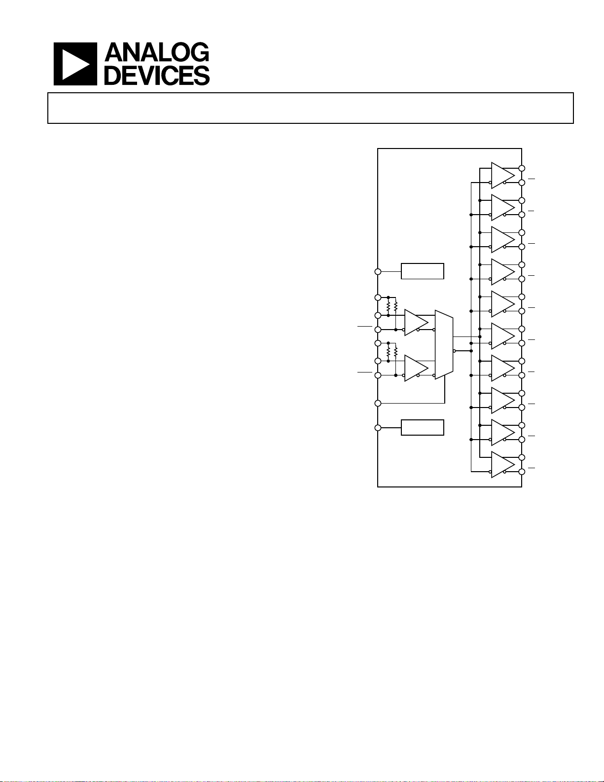
FUNCTIONAL BLOCK DIAGRAM FUNCTIONAL BLOCK DIAGRAM
ADCLK950
V
REF
VT0
CLK0
CLK0
VT1
CLK1
CLK1
IN_SEL
V
REF
0
1
REFERENCE
REFERENCE
Figure 1.
LVPECL
Q0
Q0
Q1
Q1
Q2
Q2
Q3
Q3
Q4
Q4
Q5
Q5
Q6
Q6
Q7
Q7
Q8
Q8
Q9
Q9
08279-001
Rev. A
Information furnished by Analog Devices is believed to be accurate and reliable. However, no
responsibility is assumed by Analog Devices for its use, nor for any infringements of patents or other
rights of third parties that may result from its use. Specifications subject to change without notice. No
license is granted by implication or otherwise under any patent or patent rights of Analog Devices.
Trademarks and registered trademarks are the property of their respective owners.
One Technology Way, P.O. Box 9106, Norwood, MA 02062-9106, U.S.A.
Tel: 781.329.4700 www.analog.com
Fax: 781.461.3113 ©2009–2010 Analog Devices, Inc. All rights reserved.

ADCLK950
TABLE OF CONTENTS
Features .............................................................................................. 1
Applications ....................................................................................... 1
General Description ......................................................................... 1
Functional Block Diagram .............................................................. 1
Revision History ............................................................................... 2
Specifications ..................................................................................... 3
Electrical Characteristics ............................................................. 3
Absolute Maximum Ratings ............................................................ 5
Determining Junction Temperature .......................................... 5
ESD Caution .................................................................................. 5
Thermal Performance .................................................................. 5
REVISION HISTORY
6/10—Rev. 0 to Rev. A
Changed Output Voltage Differential Parameter to Output
Voltage, Single Ended Parameter, Table 1 ..................................... 3
Changes to Output Voltage, Single Ended Parameter, Table 1 ... 3
7/09—Revision 0: Initial Version
Pin Configuration and Function Descriptions ..............................6
Typical Performance Characteristics ..............................................7
Functional Description .....................................................................9
Clock Inputs ...................................................................................9
Clock Outputs ................................................................................9
Clock Input Select (IN_SEL) Settings...................................... 10
PCB Layout Considerations ...................................................... 10
Input Termination Options ....................................................... 11
Outline Dimensions ....................................................................... 12
Ordering Guide .......................................................................... 12
Rev. A | Page 2 of 12

ADCLK950
SPECIFICATIONS
ELECTRICAL CHARACTERISTICS
Typical (Typ column) values are given for VCC − VEE = 3.3 V and TA = 25°C, unless otherwise noted. Minimum (Min column) and maximum
(Max column) values are given over the full V
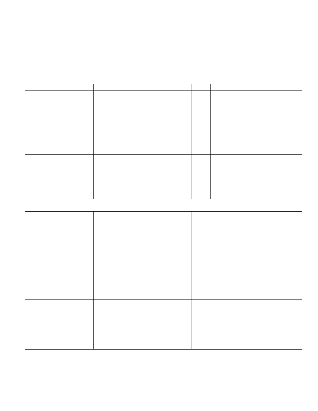
Table 1. Clock Inputs and Outputs
Parameter Symbol Min Typ Max Unit Test Conditions/Comments
DC INPUT CHARACTERISTICS
Input Common Mode Voltage V
VEE + 1.5 VCC − 0.1 V
ICM
Input Differential Range VID 0.4 3.4 V p-p ±1.7 V between input pins
Input Capacitance CIN 0.4 pF
Input Resistance
Single-Ended Mode 50 Ω
Differential Mode 100 Ω
Common Mode 50 kΩ Open VTx
Input Bias Current 20 µA
Hysteresis 10 mV
DC OUTPUT CHARACTERISTICS
Output Voltage High Level VOH V
Output Voltage Low Level VOL V
Output Voltage, Single Ended VO 610 960 mV VOH − VOL, output static
Reference Voltage V
REF
Output Voltage (VCC + 1)/2 V −500 µA to +500 µA
Output Resistance 235 Ω
− VEE = 3.3 V ± 10% and TA = −40°C to +85°C variation, unless otherwise noted.
CC
− 1.26 VCC − 0.76 V 50 Ω to (VCC − 2.0 V)
CC
− 1.99 VCC − 1.54 V 50 Ω to (VCC − 2.0 V)
CC
Table 2. Timing Characteristics
Parameter Symbol Min Typ Max Unit Test Conditions/Comments
AC PERFORMANCE
Maximum Output Frequency 4.5 4.8 GHz
See Figure 4 for differential output voltage vs.
frequency, >0.8 V differential output swing
Output Rise Time tR 40 75 90 ps 20% to 80% measured differentially
Output Fall Time tF 40 75 90 ps
Propagation Delay tPD 175 210 245 ps V
= 2 V, VID = 1.6 V p-p
ICM
Temperature Coefficient 50 fs/°C
Output-to-Output Skew1 9 28 ps
Part-to-Part Skew 45 ps VID = 1.6 V p-p
Additive Time Jitter
Integrated Random Jitter 28 fs rms BW = 12 kHz − 20 MHz, CLK = 1 GHz
Broadband Random Jitter2 75 fs rms VID = 1.6 V p-p, 8 V/ns, V
ICM
= 2 V
Crosstalk-Induced Jitter3 90 fs rms
CLOCK OUTPUT PHASE NOISE
Absolute Phase Noise
Input slew rate > 1 V/ns (see Figure 11, the
phase noise plot, for more details)
fIN = 1 GHz −119 dBc/Hz @100 Hz offset
−134 dBc/Hz @1 kHz offset
−145 dBc/Hz @10 kHz offset
−150 dBc/Hz @100 kHz offset
−150 dBc/Hz >1 MHz offset
1
The output skew is the difference between any two similar delay paths while operating at the same voltage and temperature.
2
Measured at the rising edge of the clock signal; calculated using the SNR of the ADC method.
3
This is the amount of added jitter measured at the output while two related, asynchronous, differential frequencies are applied to the inputs.
Rev. A | Page 3 of 12

ADCLK950
Table 3. Input Select Control Pin
Parameter Symbol Min Typ Max Unit
Logic 1 Voltage VIH V
Logic 0 Voltage VIL V
Logic 1 Current IIH 100 A
Logic 0 Current IIL 0.6 mA
Capacitance 2 pF
Table 4. Power
Parameter Symbol Min Typ Max Unit Test Conditions/Comments
POWER SUPPLY
Supply Voltage Requirement VCC − VEE 2.97 3.63 V 3.3 V + 10%
Power Supply Current Static
Negative Supply Current I
Positive Supply Current I
Power Supply Rejection1 PSR
Output Swing Supply Rejection2 PSR
1
Change in tPD per change in VCC.
2
Change in output swing per change in VCC.
106 130 mA VCC − VEE = 3.3 V ± 10%
VEE
346 390 mA VCC − VEE = 3.3 V ± 10%
VCC
<3 ps/V VCC − VEE = 3.3 V ± 10%
VCC
28 dB VCC − VEE = 3.3 V ± 10%
VCC
− 0.4 VCC V
CC
1 V
EE
Rev. A | Page 4 of 12
 Loading...