Ultrafast SiGe
www.BDTIC.com/ADI
FEATURES
95 ps propagation delay
7.5 GHz toggle rate
60 ps typical output rise/fall
60 fs random jitter (RJ)
On-chip terminations at both input pins
Extended industrial temperature range: −40°C to +125°C
2.5 V to 3.3 V power supply (V
APPLICATIONS
Clock and data signal restoration and level shifting
Automated test equipment (ATE)
High speed instrumentation
High speed line receivers
Threshold detection
Converter clocking
GENERAL DESCRIPTION
The ADCLK905 (one input, one output), ADCLK907 (dual one
input, one output), and ADCLK925 (one input, two outputs) are
ultrafast clock/data buffers fabricated on the Analog Devices, Inc.,
proprietary XFCB3 silicon germanium (SiGe) bipolar process.
The ADCLK905/ADCLK907/ADCLK925 feature full-swing
emi
tter coupled logic (ECL) output drivers. For PECL (positive
ECL) operation, bias V
For NECL (negative ECL) operation, bias V
V
to the negative supply.
EE
The buffers offer 95 ps propagation delay, 7.5 GHz toggle rate,
ps data rate, and 60 fs random jitter (RJ).
10 Gb
The inputs have center tapped, 100 Ω, on-chip termination
r
esistors. A V
REF
The ECL output stages are designed to directly drive 800 mV
ach side into 50 Ω terminated to V
e
differential output swing of 1.6 V.
The ADCLK905/ADCLK907/ADCLK925 are available in
16-lead LFCS
P packages.
to the positive supply and VEE to ground.
CC
pin is available for biasing ac-coupled inputs.
− VEE)
CC
− 2 V for a total
CC
to ground and
CC
ECL Clock/Data Buffers
ADCLK905/ADCLK907/ADCLK925
TYPICAL APPLICATION CIRCUITS
V
REF
V
T
D
D
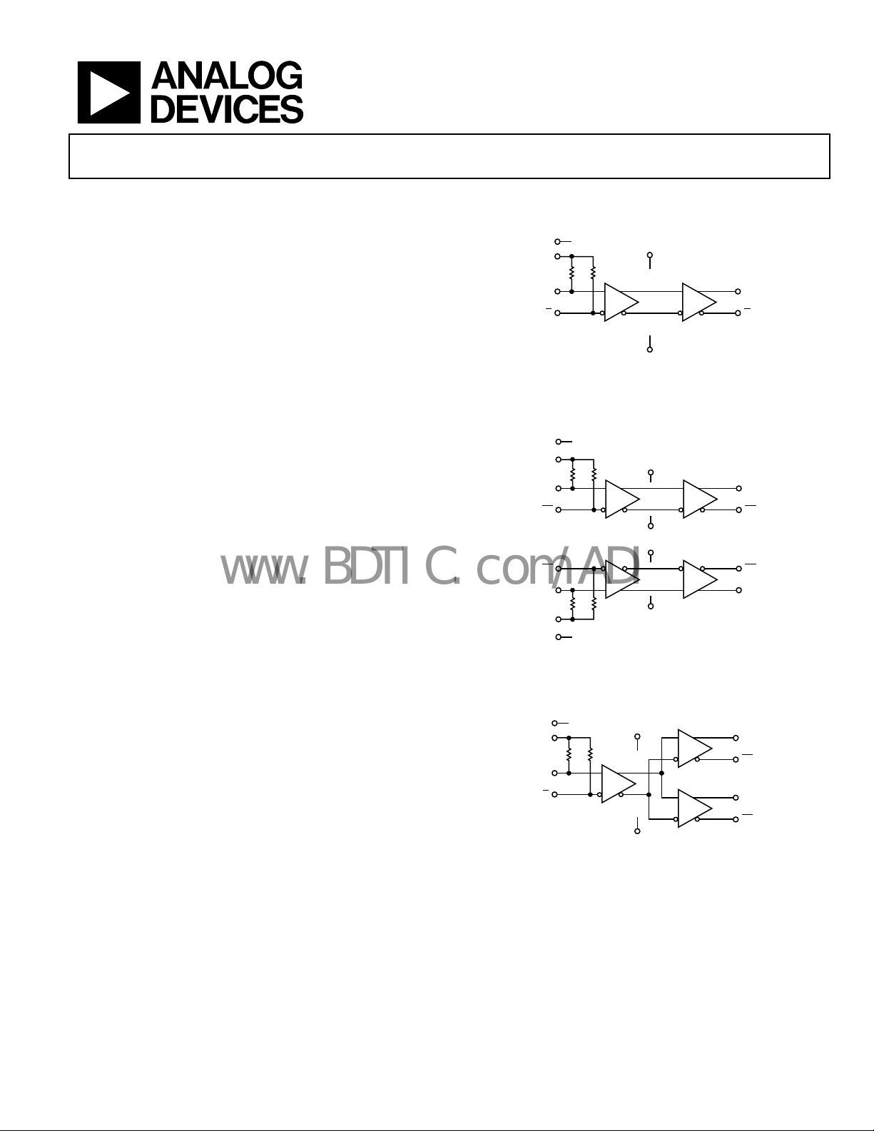
Figure 1. ADCLK905 ECL 1:1 Clock/Data Buffer
V
1
REF
VT1
D1
D1
D2
D2
VT2
V
2
REF
Figure 2. ADCLK907 ECL Dual 1:1 Clock/Data Buffer
V
REF
V
T
D
D
Figure 3. ADCLK925 ECL 1:2 Clock/Data Fanout Buffer
V
CC
Q
Q
V
EE
V
CC
V
EE
V
EE
V
CC
V
CC
V
EE
Q1
Q1
Q2
Q2
Q1
Q1
Q2
Q2
06318-001
06318-002
06318-003
Rev. 0
Information furnished by Analog Devices is believed to be accurate and reliable. However, no
responsibility is assumed by Anal og Devices for its use, nor for any infringements of patents or ot her
rights of third parties that may result from its use. Specifications subject to change without notice. No
license is granted by implication or otherwise under any patent or patent rights of Analog Devices.
Trademarks and registered trademarks are the property of their respective owners.
One Technology Way, P.O. Box 9106, Norwood, MA 02062-9106, U.S.A.
Tel: 781.329.4700 www.analog.com
Fax: 781.461.3113 ©2007 Analog Devices, Inc. All rights reserved.

ADCLK905/ADCLK907/ADCLK925
www.BDTIC.com/ADI
TABLE OF CONTENTS
Features.............................................................................................. 1
Applications....................................................................................... 1
General Description ......................................................................... 1
Typical Application Circuits........................................................... 1
Revision History ............................................................................... 2
Specifications..................................................................................... 3
Electrical Characteristics ............................................................. 3
Absolute Maximum Ratings............................................................ 5
Thermal Resistance ...................................................................... 5
ESD Caution.................................................................................. 5
Pin Configurations and Function Descriptions ........................... 6
REVISION HISTORY
8/07—Revision 0: Initial Version
Typical Performance Characteristics..............................................8
Applications Information.............................................................. 11
Power/Ground Layout and Bypassing..................................... 11
Output Stages............................................................................... 11
Optimizing High Speed Performance..................................... 11
Buffer Random Jitter.................................................................. 11
Typical Application Circuits ......................................................... 12
Evaluation Board Schematic......................................................... 13
Outline Dimensions....................................................................... 14
Ordering Guide .......................................................................... 14
Rev. 0 | Page 2 of 16

ADCLK905/ADCLK907/ADCLK925
www.BDTIC.com/ADI
SPECIFICATIONS
ELECTRICAL CHARACTERISTICS
Typical (Typ) values are given for VCC − VEE = 3.3 V and TA = 25°C, unless otherwise noted. Minimum (Min) and maximum (Max) values are
given over the full V
Table 1.
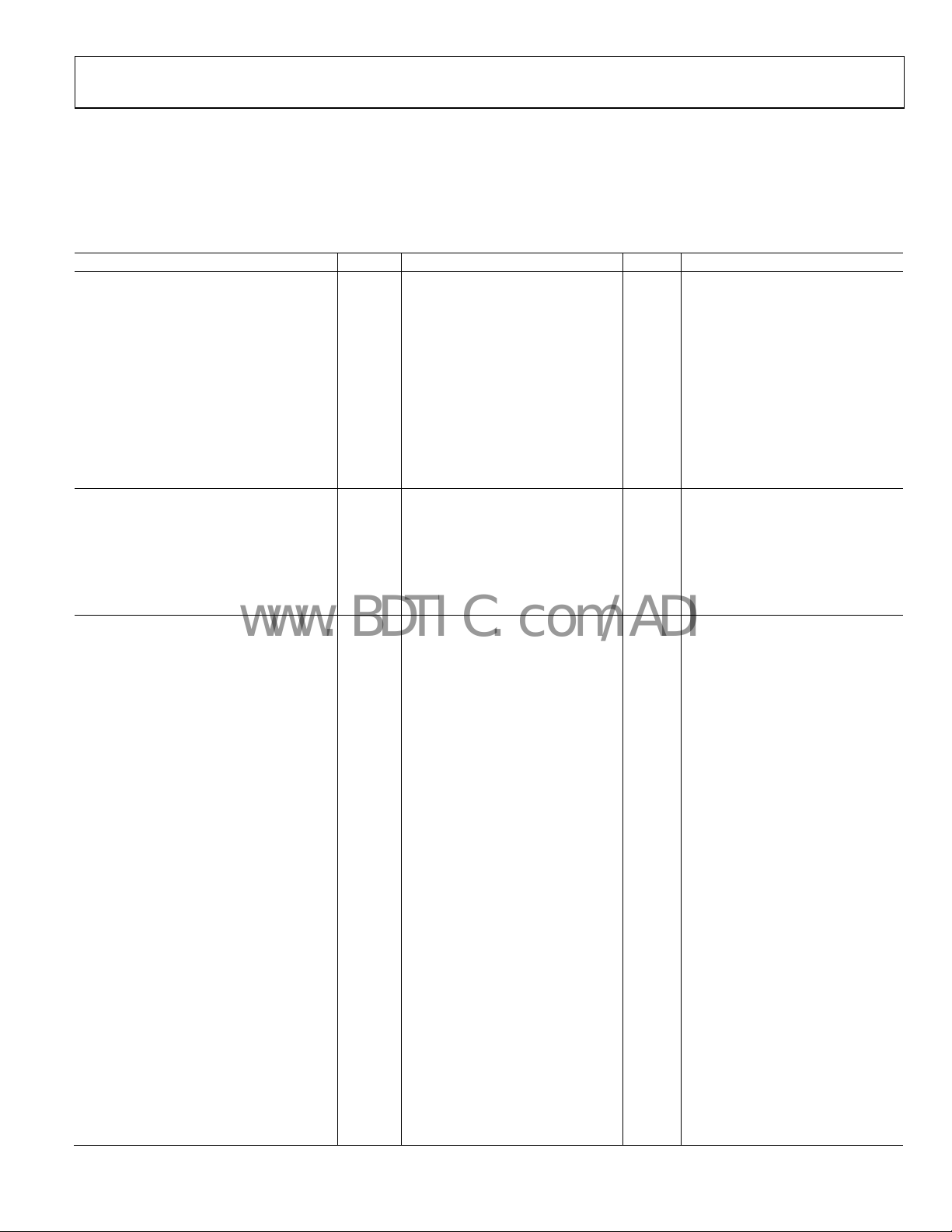
Parameter Symbol Min Typ Max Unit Conditions
DC INPUT CHARACTERISTICS
Input Voltage High Level VIH V
Input Voltage Low Level VIL V
Input Differential Range VID 0.2 3.4 V p-p −40°C to +85°C
V
Input Capacitance CIN 0.4 pF
Input Resistance, Single-Ended Mode 50 Ω
Input Resistance, Differential Mode 100 Ω
Input Resistance, Common Mode 50 kΩ Open VT
Input Bias Current 20 μA
DC OUTPUT CHARACTERISTICS
Output Voltage High Level VOH V
Output Voltage Low Level VOL V
Output Voltage Differential VOD 610 1040 mV 50 Ω to (VCC − 2.0 V)
Reference Voltage V
Output Voltage (VCC + 1)/2 V −500 μA to +500 μA
Output Resistance 250 Ω
AC PERFORMANCE
Propagation Delay tPD 70 95 125 ps VCC = 3.3 V ± 10%,
70 95 125 ps VCC = 2.5 V ± 5%,
Propagation Delay Temperature Coefficient 50 fs/°C
Propagation Delay Skew (Output to Output)
ADCLK907
Propagation Delay Skew (Output to Output)
ADCLK925
Propagation Delay Skew (Device to Device) 35 ps VID = 0.5 V
Toggle Rate 6 7.5 GHz >0.8 V differential output swing,
6.5 GHz >0.8 V differential output swing,
Random Jitter RJ 60 fs rms VID = 1600 mV, 8 V/ns, V
Rise/Fall Time tR/tF 30 85 ps 20%/80%
Additive Phase Noise
622.08 MHz −138 dBc/Hz @10 Hz offset
−144 dBc/Hz @100 Hz offset
−152 dBc/Hz @1 kHz offset
−159 dBc/Hz @10 kHz offset
−161 dBc/Hz @100 kHz offset
−161 dBc/Hz >1 MHz offset
122.88 MHz −135 dBc/Hz @10 Hz offset
−145 dBc/Hz @100 Hz offset
−153 dBc/Hz @1 kHz offset
−160 dBc/Hz @10 kHz offset
−161 dBc/Hz @100 kHz offset
−161 dBc/Hz >1 MHz offset
− VEE = 3.3 V ± 10% and TA = −40°C to +125°C variation, unless otherwise noted.
CC
+ 1.6 VCC V
EE
V
EE
0.2 2.8 V p-p 85°C to 125°C
ID
− 1.26 VCC − 0.76 V 50 Ω to (VCC − 2.0 V)
CC
− 1.99 VCC − 1.54 V 50 Ω to (VCC − 2.0 V)
CC
REF
− 0.7 V
CC
15 ps VID = 0.5 V
10 ps VID = 0.5 V
(±1.7 V between input pins)
(±1.4 V between input pins)
V
= V
, VID = 0.5 V p-p
ICM
REF
V
= V
ICM
V
CC
V
CC
, VID = 0.5 V p-p
REF
= 3.3 V ± 10%
= 2.5 V ± 5%
= 1.85 V
ICM
Rev. 0 | Page 3 of 16

ADCLK905/ADCLK907/ADCLK925
www.BDTIC.com/ADI
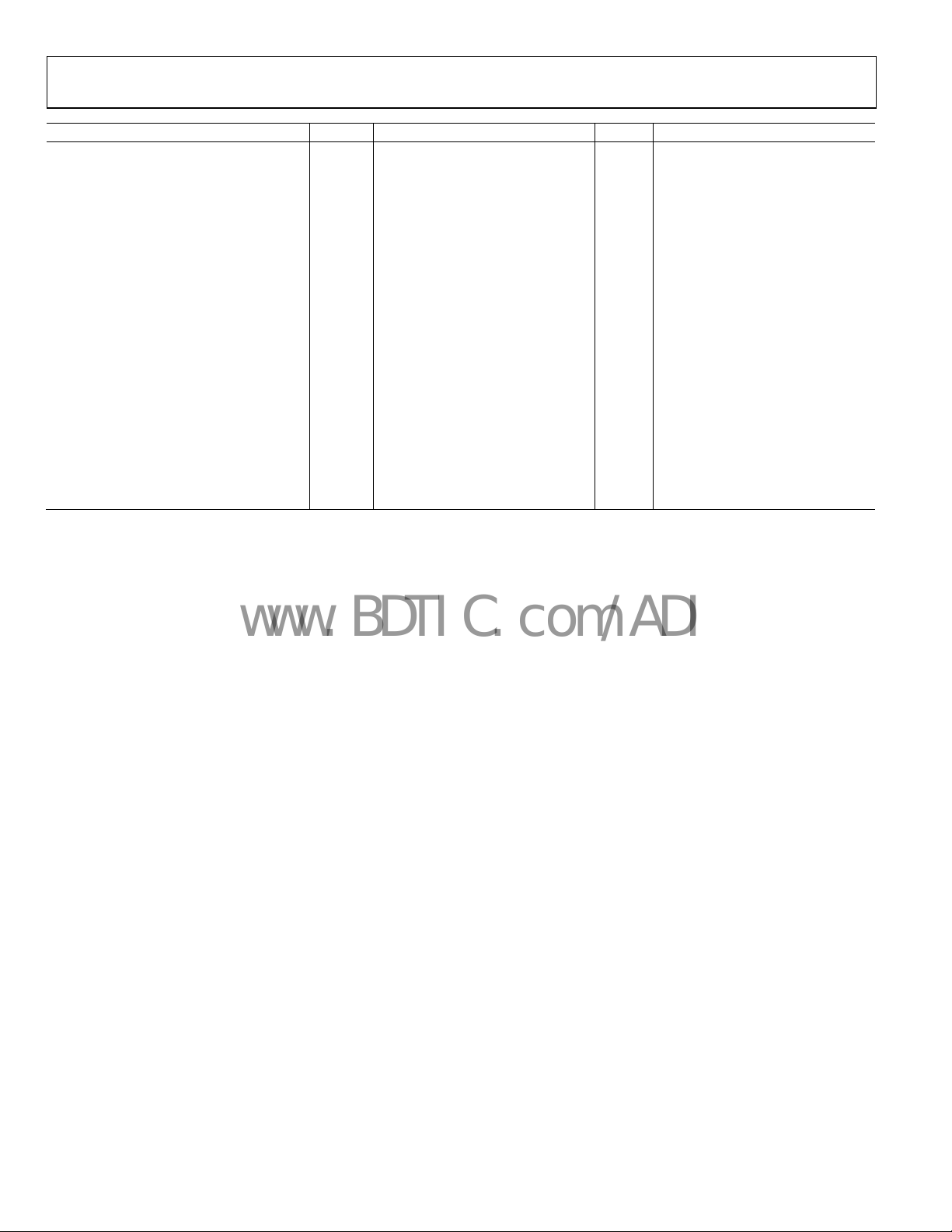
Parameter Symbol Min Typ Max Unit Conditions
POWER SUPPLY
Supply Voltage Requirement VCC − VEE 2.375 3.63 V 2.5 V − 5% to 3.3 V + 10%
Power Supply Current Static
ADCLK905
Negative Supply Current I
25 40 mA
Positive Supply Current I
48 63 mA
ADCLK907
Negative Supply Current I
50 80 mA
Positive Supply Current I
96 126 mA
ADCLK925
Negative Supply Current I
31 51 mA
Positive Supply Current I
77 97 mA
Power Supply Rejection
Output Swing Supply Rejection
1
Change in TPD per change in VCC.
2
Change in output swing per change in VCC.
1
2
24 mA VCC − VEE = 2.5 V
VEE
V
− VEE = 3.3 V ± 10%
CC
47 mA VCC − VEE = 2.5 V
VCC
V
− VEE = 3.3 V ± 10%
CC
48 mA VCC − VEE = 2.5 V
VEE
V
− VEE = 3.3 V ± 10%
CC
94 mA VCC − VEE = 2.5 V
VCC
V
− VEE = 3.3 V ± 10%
CC
29 mA VCC − VEE = 2.5 V
VEE
V
− VEE = 3.3 V ± 10%
CC
76 mA VCC − VEE = 2.5 V
VCC
V
− VEE = 3.3 V ± 10%
CC
PSR
3 ps/V VCC − VEE = 3.0 V ± 20%
VCC
PSR
26 dB VCC − VEE = 3.0 V ± 20%
VCC
Rev. 0 | Page 4 of 16

ADCLK905/ADCLK907/ADCLK925
www.BDTIC.com/ADI
ABSOLUTE MAXIMUM RATINGS
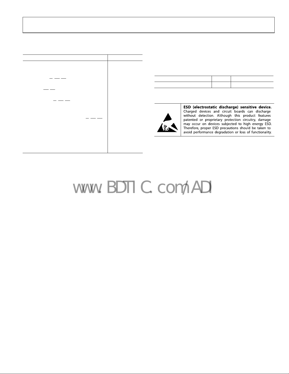
Table 2.
Parameter Rating
Supply Voltage
VCC − VEE 6.0 V
Input Voltage
D (D1, D2), D (D1, D2)
D1, D2, D1, D2 to VT Pin
(CML or PECL Termination)
D (D1, D2) to D (D1, D2)
Maximum Voltage on Output Pins VCC + 0.5 V
Maximum Output Current 35 mA
Input Termination, VT to D (D1, D2), D (D1, D2)
Voltage Reference, V
Temperature
Operating Temperature Range, Ambient −40°C to +125°C
Operating Temperature, Junction 150°C
Storage Temperature Range −65°C to +150°C
Stresses above those listed under Absolute Maximum Ratings
may cause permanent damage to the device. This is a stress
rating only; functional operation of the device at these or any
other conditions above those indicated in the operational
section of this specification is not implied. Exposure to absolute
maximum rating conditions for extended periods may affect
device reliability.
V
REF
V
− 0.5 V to
EE
+ 0.5 V
V
CC
±40 mA
±1.8 V
±2 V
− VEE
CC
THERMAL RESISTANCE
θJA is specified for the worst-case conditions, that is, a device
soldered in a circuit board for surface-mount packages.
Table 3. Thermal Resistance
Package Type θJA Unit
16-lead LFCSP 70 °C/W
ESD CAUTION
Rev. 0 | Page 5 of 16
 Loading...