

Page 1

a ADSP-21990: Utilization of the Analog to Digital Converter (ADC) AN21990-05
a
ADSP-21990: Utilization of the
Analog to Digital Converter (ADC)
AN21990-05
© Analog Devices Inc., April 2002 Page 1 of 7
Page 2

a ADSP-21990: Utilization of the Analog to Digital Converter (ADC) AN21990-05
Table of Contents
SUMMARY...................................................................................................................... 3
1 IMPLEMENTATION OF THE ADC LIBRARY ROUTINE......................................... 3
1.1 Usage of ADC routine ....................................................................................................................................3
1.2 Usage of DSP registers ...................................................................................................................................3
1.3 Configuring the ADC block...........................................................................................................................4
1.3.1 adc.h .............................................................................................................................................................4
1.3.2 adc.dsp .........................................................................................................................................................4
2 SOFTWARE EXAMPLE: UTILIZATION OF THE ADC BLOCK TO GENERATE
THREE-PHASE SINE-WAVE PWM................................................................................ 4
2.1 Main.dsp..........................................................................................................................................................4
2.2 Main.h..............................................................................................................................................................5
3 EXPERIMENTAL RESULTS.................................................................................... 5
© Analog Devices Inc., April 2002 Page 2 of 7
Page 3
a ADSP-21990: Utilization of the Analog to Digital Converter (ADC) AN21990-05
Summary
This application note demonstrates the usage of the pipeline flash Analog to Digital Converter (ADC)
system
1
on the ADSP-21990. Section one will discuss the ADC library routines. In section two, an
example will be used to demonstrate the usage of these routines. The last section shows some
experimental results.
1 Implementation of the ADC library routine
1.1 Usage of ADC routine
In this library, two routines are defined for initialising the ADC block and reading the ADC channel
values. It is developed as an easy-to-use library, which has to be linked to the user’s application. The
library consists of two files. The file “adc.dsp” contains the assembly code of the subroutines. The block
has to be compiled and then linked to an application. The user has to include the header file “adc.h”,
which provides the function-like call to the subroutine. The following table shows the macro that is
defined in this library.
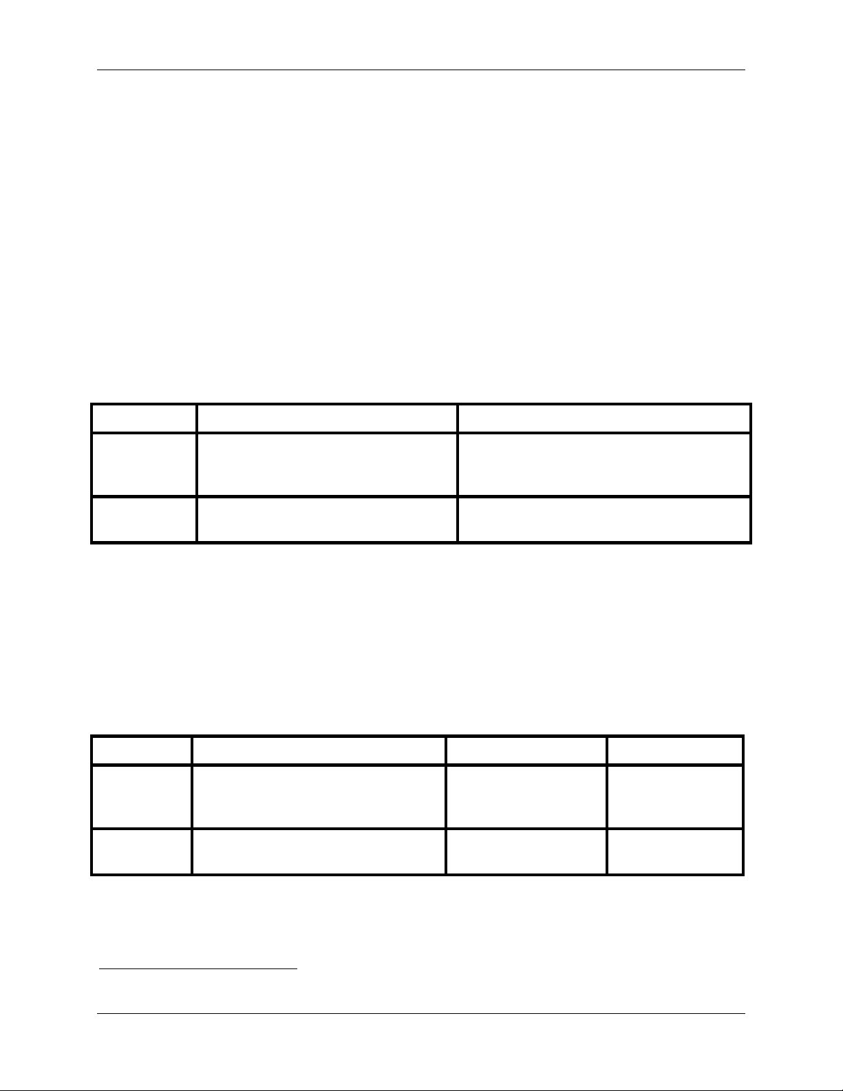
Operation Usage Explanation
Initialisation
Read ADC
ADC_Init(ADC_Number_of_samples,
ADC_EOC_interrupt_label)
ADC_Read(ADC_DATAX,
Offset_0to3 or Offset_4to7)
Initialise the ADC block, including
configuring the ADC end of conversion
interrupt
Reading the ADC channel values, with the
offset values being taken into account
Table 1 Implementation Routine
This routine requires a configuration constant from the main include-file “main.h” that comes with every
application note. Section 2 shows an example of usage of this library. For more information regarding this
routine, see the comments in the “adc.h” and the “adc.dsp” files.
1.2 Usage of DSP registers
The macro listed in the Table 1 is based on the subroutine listed in Table 2. This subroutine will be
discussed in the following section. The following table gives an overview of what DSP registers are used
in this macro:
Subroutine Inputs
ADC_Init_
ADC_Scale_
Table 2 Input and output format, modified registers in the ADC library routines
ADC_Number_of_samples: the
number of samples to be taken for
calculating the offset
None
Outputs Modified registers
mr1 = Offset_0to3
sr1 = Offset_4to7
ar = ADC channel
value after offset
ar, ay0, ay1, mr,
mx0, my0, sr,
ar, ay0
1
Please refer to the ADSP-21990 hardware reference manual for information on the ADC block
© Analog Devices Inc., April 2002 Page 3 of 7
Page 4

a ADSP-21990: Utilization of the Analog to Digital Converter (ADC) AN21990-05
1.3 Configuring the ADC block
1.3.1 adc.h
The library may be accessed by including the header file “adc.h” into the application code. Two macros,
the ADC_Init and the ADC_Read are defined in this file. The ADC_Init loads the value of the number of
samples used for calculating the ADC initial offsets and also sets the interrupt vector for the ADC end of
conversion (EOC) interrupt. (Another macro called the Set_InterruptVector is used; which is defined in
the general-purpose file “macro.h”). It then provides a call to the ADC_Init_ routine, which is defined in
the adc.dsp file. In the ADC_Read macro, the value of the required ADC channel is loaded into the DSP,
and then a call is made to the ADC_Scale_ routine for calculating the actual ADC channel value. For
more information on the “adc.h” file, please refer to the comments in the file.
1.3.2 adc.dsp
In this file, the ADC_Init_ and the ADC_Scale routines are defined. It obtains the system parameters and
the ADC configuration value, which is the ADC_Number_of_samples, defined in “main.h”(refer to
Section 2.2). The user can define this value to specify the number of samples to be taken from each
channel for calculating the offset values for the ADC. Then the ADC_Init_ initialises the ADC block. In
the ADSP-21990, there are 12 user-defined interrupt lines, from USR0 (highest priority) to USR11
(lowest priority). In this routine, the ADC EOC interrupt is assigned to USR2. Then the ADC is set to the
offset calibration mode, with software conversion start. Then the routine enters a loop such that it will
calculate the average values of VIN0 to VIN3 and VIN4 to VIN7, which are the Offset_0to3 and
Offset_4to7 respectively. When the offsets are ready, the routine configures the ADC to simultaneous
sampling mode with PWMSync conversion start.
In the ADC_Scale_ routine, the actual value of the ADC channel is calculated by subtracting the offset
from the value read in the ADC channel. For more information on the “adc.dsp” program, please refer to
the comments in the file.
2 Software Example: Utilization of the ADC block to generate Three-
Phase Sine-Wave PWM
This example is based on another application note2. The user can specify the fundamental frequency of
the waveform in the “main.dsp” program. The only difference is that the amplitude of the waveform is
controlled by the ADC channel value.
2.1 Main.dsp
It contains the initialisation and ADC end of conversion and PWMTRIP interrupt service routines.
Besides the “adc.h”, the “pwm.h” and “main.h”, since sinusoidal calculation is also required, the
“trigono.dsp” file is also included. Some constants and variables (including the amplitude factor, which
will be obtained from the ADC channel) are defined. In this example, the fundamental frequency is 60Hz.
At the start of the program, initialisations such as setting the data memory page registers to accessing the
internal memory, PWM initialisation (see the “pwm.h’ and “pwm.dsp” files for details) and the ADC
initialisation (see the “adc.h’ and “adc.dsp” files for details) are accomplished. Then only the PWMTRIP
and the ADC_EOC interrupts are enabled while the PWMSync interrupt is disabled. (User can enable this
by enabling USR1 interrupt).
2
Please refer to the application note “Generation of Three-Phase Sinewave PWM patterns” for details.
© Analog Devices Inc., April 2002 Page 4 of 7
Page 5

a ADSP-21990: Utilization of the Analog to Digital Converter (ADC) AN21990-05
The implementation of this example is performed in the ADC_EOC interrupt service routine. Since the
ADC sampling is set to be PWMSync triggered, that means the ADC_EOC is executed at the rate same as
the PWM switching rate (20kHz here). This interrupt service routine is used such that the most up-to-date
data obtained from the ADC channel is used
3
.In this routine, firstly, the ADC interrupt status in the ADC
status register is cleared. Then the ADC VIN0 value is read with the offset value (Offset_0to3 in this
case) being taken into account to obtain the actual ADC VIN0 value. This value is the amplitude factor
that is used to adjust the amplitude of the PWM waveform. The phase angle Theta is incremented and
stored for the next interrupt. Sin(Theta) is computed for each phase such that phase A, B and C are 120
o
apart. The duty cycle for each phase is computed, and then written to the duty cycle registers.
In the PWMTRIP interrupt service routine, the users can define what to implement in case of a PWM
fault. In this example, the status bit of the PWMTRIP interrupt in the PWM status register is cleared.
For more details on the “main.dsp”, please refer to the comments in the file.
2.2 Main.h
As discussed before, the configuration of the ADC block requires a constant, which is defined in the
“main.h” file. The use of this file is to define general system parameters and constants, such as the crystal
clock [kHz], core clock [kHz] and the peripheral clock [kHz] (also denoted as H
constants required by the library files will be defined here. In this case, the ADC_Number_of_samples
(30 samples are used from each channel for calculating the offset values) and the constants needed by the
PWM library, such as the PWM switching frequency [Hz], the dead time [nsec] and the PWM sync pulse
time [nsec] will be included in this file. Two files, the “ADSP-21990.h” and the “macro.h” are also
included in the “main.h” file. The “ADSP-21990.h” defines the peripheral registers of the ADSP-21990
while the “macro.h” defines the most commonly used macro.
). Besides, any
clk
4
3 Experimental Results
The results below show the waveforms on the PWM channels while running this example with the ADC
VIN0 input changing. Here, the crystal clock is 25MHz, the peripheral clock (H
switching frequency = 20kHz, PWM dead time = 2µs and PWM sync pulse width = 440ns. The
fundamental frequency of the sine wave is 60Hz. In this example, internal reference voltage is used
(which is 1V) and the input voltage range into the ADC through the EZ board is from –Vref to +Vref,
hence voltage input range from –1V to +1V correspond to –1 to +1 in 1.15 value. In Figure 1, one can see
the PWM waveforms of channel A when the PWM amplitude factor is 100% (achieved by applying +1V
into the ADC VIN0). Figure 2 shows the PWM patterns when the amplitude factor is–50%. From Figure
3, an amplitude factor of 50% is applied and it shows that the three phases are 120
3
If the PWMSync interrupt service routine is used instead, the user has to make sure all the ADC samples
from the previous cycle are saved into memory before the new samples are converted.
4
Note that this number can be any positive integer value and does not have to be a power to two.
) is 12.5MHz. PWM
clk
o
apart.
© Analog Devices Inc., April 2002 Page 5 of 7
Page 6

a ADSP-21990: Utilization of the Analog to Digital Converter (ADC) AN21990-05
Figure 1 Filtered sine PWM outputs Ch1: AH, Ch2:AL CH4: ADC VIN0 input = amplitude factor
(100%)
Figure 2 Filtered PWM outputs, Ch1: AH, Ch2: AL, Ch4: ADC VIN0 input = amplitude factor
(-50%)
© Analog Devices Inc., April 2002 Page 6 of 7
Page 7

a ADSP-21990: Utilization of the Analog to Digital Converter (ADC) AN21990-05
Figure 3 PWM outputs, Ch1: AH, Ch2:BH, CH3:CH, CH4: ADC VIN0 input = amplitude factor
(50%)
© Analog Devices Inc., April 2002 Page 7 of 7
 Loading...