

Audio Codec
Preliminary Technical Data
FEATURES
Stereo Analog to Digital Converter (ADC)
Supports 48/96 kHz Sample Rates
102 dB Dynamic Range
Single-Ended Input
Automatic Level Control
Stereo Digital to Analog Converter (DAC)
Supports 32/44.1/48/96/192 kHz Sample Rates
103 dB Dynamic Range
Differential Output
Asynchronous operation of ADC and DAC
Stereo Sample Rate Converter (SRC)
Input/Output Range - 8 - 96 kHz
140 dB Dynamic Range
Digital Interfaces
Record
Playback
Aux Record
Aux Playback
S/PDIF (IEC60958) Input & Output
Digital Interface Receiver (DIR)
Digital Interface Transmitter (DIT)
PLL based Audio MCLK Generators
Generates Required DVDR System MCLKs
Device Control via SPI compatible serial port
64-Lead LQFP Package
APPLICATIONS
DVD-Recordable
All Formats
CD-R/W
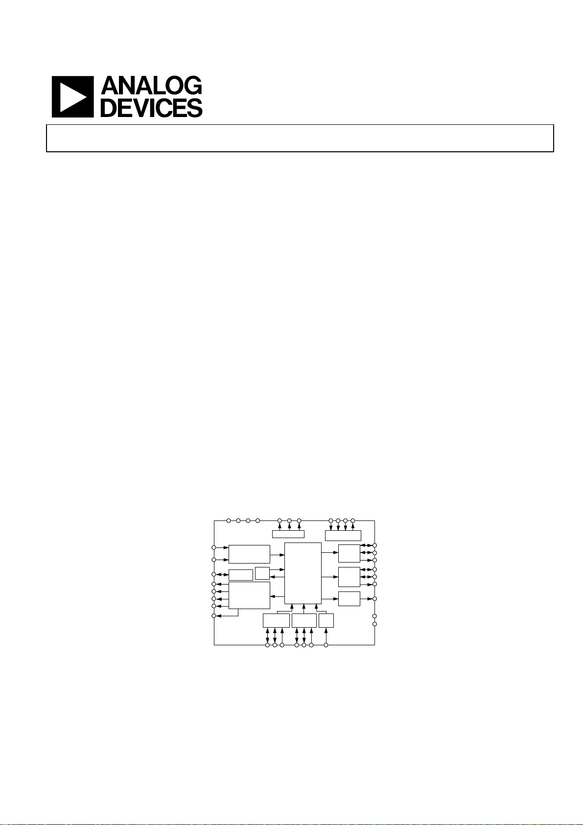
PRODUCT OVERVIEW
The ADAV802 is a stereo audio codec intended for applications,
such as DVD or CD recorders, requiring high performance,
flexible and cost effective playback and record functionality.
The ADAV802 features Analog Devices proprietary, high
performance converter cores to provide record (ADC), playback
(DAC) and format conversion (SRC) in a single chip. The
ADAV802 record channel features variable input gain to allow
for adjustment of recorded input levels and Automatic Level
Control, followed by a high performance stereo ADC whose
digital output is sent to the record interface. The record channel
also features Level Detectors which can be used in feedback
loops to adjust input levels for optimum recording. The
playback channel features a high performance stereo DAC with
independent digital volume control.
The Sample Rate Converter (SRC) provides high performance
sample-rate conversion to allow inputs and outputs requiring
different sample rates to be matched. The SRC input can be
selected from Playback, Auxiliary, DIR or ADC (record). The
SRC output can be applied to the Playback DAC, both main and
Auxiliary record channels and a DIT. (continued on Page 12)
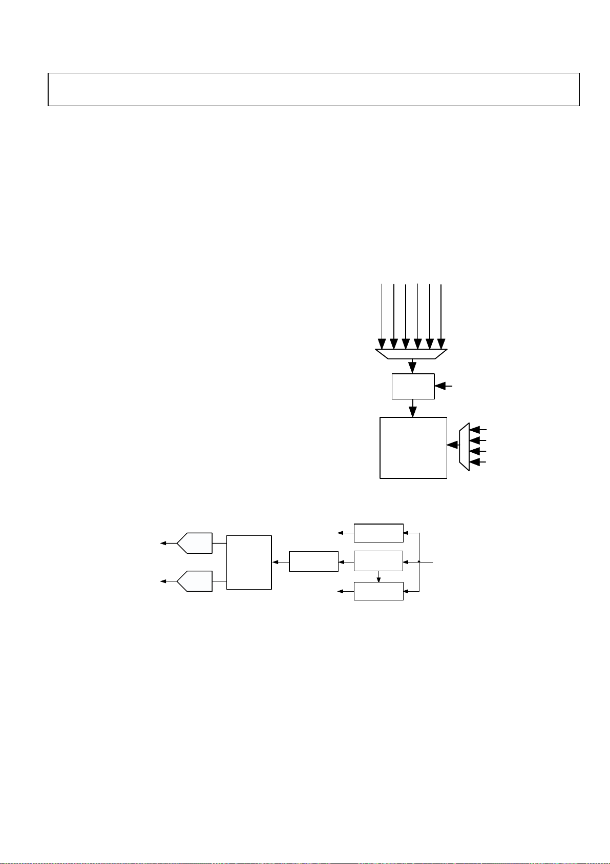
FUNCTIONAL BLOCK DIAGRAM
1
2
3
K
K
I
O
T
K
K
L
L
U
N
C
I
X
C
O
X
M
M
K
L
L
L
C
C
C
S
S
S
Y
Y
Y
S
S
S
H
C
T
K
T
U
L
A
N
C
O
L
I
C
C
C
C
For Recordable DVD
ADAV802
VINL
VINR
VREF
VOUTLN
VOUTLP
VOUTRN
VOUTRP
FILTD
Rev. Pr G
Information furnished by Analog Devices is believed to be accurate and reliable.
However, no responsibility is assumed by Analog Devices for its use, nor for any
infringements of patents or other rights of third parties that may result from its use.
Specifications subject to change without notice. No license is granted by implication
or otherwise under any patent or patent rights of Analog Devices. Trademarks and
registered trademar ks are the property of their respective orners.
Analog to Digital
Converter
Reference SRC
Digital to Analog
Converter
ADAV802
Playback
Data Input
K
L
C
R
L
I
PLL
SwitchingMatrix
K
A
T
L
A
C
D
B
I
S
I
Figure 1.
Control
Registers
Record
Data
Digital
Input/Output
(Datapath)
Aux Data
Input
K
K
L
L
C
C
B
R
L
X
X
U
U
A
I
A
I
A
T
A
D
S
X
U
A
I
Output
Aux Data
Output
DIT
DIR
N
I
R
I
D
One Technology Way, P.O. Box 9106, Norwood, MA 02062-9106, U.S.A.
Tel: 781.329.4700
Fax: 781.326.8703 © 2004 Analog Devices, Inc. All rights reserved.
OLRCLK
OBCLK
OSDATA
OAUXLRCLK
OAUXBCLK
OAUXSDAT A
DITOUT
ZEROL/INT
ZEROR
802-0001
www.analog.com

ADAV802 Preliminary Technical Data
TABLE OF CONTENTS
Specifications..................................................................................... 3
Hardware Model......................................................................... 17
Timing Specifications....................................................................... 7
Absolute Maximum Ratings............................................................ 8
ESD Caution.................................................................................. 8
Pin Configuration and Function Descriptions............................. 9
Functional Description.................................................................. 12
ADC Section ............................................................................... 12
DAC Section.................................................................................... 15
SRC Functional Overview ............................................................. 16
Theory of Operation ..................................................................16
Conceptual High Interpolation Model.................................... 16
REVISION HISTORY
The Sample Rate Converter Architecture............................... 17
PLL Section ................................................................................. 18
SPDIF Transmitter AND Receiver........................................... 20
Serial Data Ports......................................................................... 25
Clocking Scheme........................................................................ 25
Data Path..................................................................................... 25
Interface Control........................................................................ 26
Outline Dimensions....................................................................... 53
Ordering Guide .......................................................................... 53
Rev. Pr G | Page 2 of 53

Preliminary Technical Data ADAV802
SPECIFICATIONS
Table 1. Test Conditions Unless Otherwise Noted
Supply Voltage
Analog +3.3 V
Digital +3.3 V
Ambient Temperature 25°C
Master Clock (XIN) 12.288 MHz
Measurement Bandwidth 20 Hz to 20 kHz
Word Width (All Converters) 24-bits
Load Capacitance on Digital Outputs 100 pF
ADC Input Frequency 997Hz at −1 dBFS
DAC Output Frequency 997Hz at −1 dBFS
Digital Input: Slave Mode, I2S Justified Format
Digital Output: Master Mode, I2S Justified Forma
Table 2. P GA S e ction
Min Typ Max Unit Conditions
Input Impedance 4
kΩ
Minimum Gain 0 dB
Maximum Gain 24 dB
Gain Step 0.5 dB
Gain Step Error TBD dB
Table 3. Reference Section
Min Typ Max Unit Conditions
Absolute Voltage, V
V
Temperature Coefficient
REF
1.5 V
REF
TBD
ppm/
°C
Table 4. A D C S e ction
1
Min Typ Max Unit Conditions
Number of Channels 2
Resolution 24 Bits
Dynamic Range −60 dB Input
Unweighted 98 100 dB
A-Weighted 99 102 dB
Total Harmonic Distorton + Noise −85 dB Input = −1.0 dBFS
Analog Input
Input Range (± Full Scale) 1.0 V
V
1.5 V
REF
RMS
DC Accuracy
Gain Error −1 dB
Interchannel Gain Mismatch 0.01 dB
Gain Drift 100 ppm/°C
Offset TBD mV
Crosstalk (EIAJ Method) 100 dB
Volume Control Step Size (256 Steps) 0.39 % per step
Maximum Volume Attenuation -48 dB
Group Delay TBD µS
1
The figures quoted are target specifications and subject to change before release
Rev. Pr G | Page 3 of 53

ADAV802 Preliminary Technical Data
Table 5. ADC Low-Pass Digital Decmation Filter Characteristics1
Sample Rate Pass Band Stop Band Stop Band Pass Band
(kHz) Frequency (kHz) Frequency (kHz) Attenuation (dB) Ripple (dB)
48 0.45314 × fS 0.54648 × fS 120 ±0.01
96 TBD × fS TBD × fS TBD ±TBD
1
Guaranteed by Design
Table 6. ADC High-Pass Digital Filter Characteristics (f
Min Typ Max Units
Cutoff Frequency 0.9 Hz
Table 7 . SR C S ec tio n
Min Typ Max Unit Conditions
Resolution 24 Bits
Sample Rate 8 96 kHz XIN = 27MHz
Maximum Sample Rate Ratios
Minimum SRC MCLK 138 × f
Upsampling 1:8
Downsampling 7.75:1
Dynamic Range 20 Hz to fS/2, 1 kHz, –60 dBFS Input
Unweighted 120 dB Worst Case - 96 kHz:8 kHz
A-Weighted 125 dB Worst Case - 96 kHz:8 kHz
Total Harmonic Distortion + Noise −110 dB 20 Hz to fS/2, 1 kHz, 0 dBFS Input
Table 8 . DAC Se cti o n
1
Min Typ Max Unit Conditions
Number of Channels 2
Resolution 24 Bits
Dynamic Range (20 Hz to 20 kHz, −60 dB Input)
Unweighted 100 dB
A-Weighted TBD 103 dB
A-Weighted TBD dB fS = 96 KHz
Total Harmonic Distorton + Noise −96 dB Digital Input = −1.0 dBFS
Total Harmonic Distorton + Noise TBD dB Digital Input = −1.0 dBFS, fS = 96 KHz
Analog Outputs
Output Range (± Full Scale) 1.0 Vrms
Output Resistance TBD
Common Mode Output Voltage 1.5 V
DC Accuracy
Gain Error −1 dB
Interchannel Gain Mismatch 0.01 dB
Gain Drift 25 ppm/°C
Crosstalk (EIAJ Method) 125 dB
Phase Deviation TBD Degrees
Mute Attenuation −63 dB
Volume Control Step Size (128 Steps) 0.5 dB
Group Delay TBD µs
1
The figures quoted are target specifications and subject to change before release
= 48 kHz)
S
S-MAX
Ω
f
S-MAX
output sample rate
is the greater of the input or
Rev. Pr G | Page 4 of 53

Preliminary Technical Data ADAV802
Table 9. DAC Low-Pass Digital Interpolation Filter Characteristics
Sample Rate Pass Band Stop Band Stop Band Pass Band
(kHz) Frequency (kHz) Frequency (kHz) Attenuation (dB) Ripple (dB)
44.1 0.4535 × fS 0.5464 × fS 70 ±0.002
48 0.4541 × fS 0.5464 × fS 70 ±0.002
96 0.4161 × fS 0.5927 × fS 70 ±0.005
Table 10. PLL Section
Min Typ Max Unit Conditions
Master Clock Input Frequency 27/54 MHz
Generated System Clocks
MCLKO 27/54 MHz
SYSCLK1 256 768 × fS
SYSCLK2 256 768 × fS
SYSCLK3 256 512 × fS 256/512 × 32/44.1/48 kHz1
Jitter
SYSCLK1 TBD ps rms
SYSCLK2 TBD ps rms
SYSCLK3 TBD ps rms
1
Sample Frequency can be doubled
Table 11. DIR Section
Min Typ Max Unit Condition
Input Sample Frequency 27.2 220 kHz
DIR-MCLK Frequency TBD MHz
DIR-MCLK Jitter TBD ps
Differential Input Voltage TBD mV
Table 12. DIT Section
Min Typ Max Unit Condition
Output Sample Frequency 27.2 220 kHz
Table 13. Digital I/O
Min Typ Max Unit Condition
Input Voltage HI (VIH) 2.0 DVDD V
Input Voltage LO (VIL) 0.8 V
Input Leakage (IIH@ VIH = 3.3 V) 10 µA
Input Leakage (IIL@ VIL = 0 V) 10 µA
Output Voltage HI (VOH @ IOH = 1 mA) 2.4 V
Output Voltage LO (VOL @ IOL = -1 mA) 0.4 V
Input Capacitance 15 pF
256/384/512/768 ×
32/44.1/48 kHz
256/384/512/768 ×
32/44.1/48 kHz
1
1
Rev. Pr G | Page 5 of 53

ADAV802 Preliminary Technical Data
Table 1 4. Po w e r
Min Typ Max Unit Condition
Supplies
Voltage, AVDD 3.0 3.3 3.6 V
Voltage, DVDD 3.0 3.3 3.6 V
Voltage, ODVDD 3.0 3.3 3.6 V
Analog Current 45 mA All Supplies at 3.6V
Digital Current, DVDD 56 mA All Supplies at 3.6V
Digital Interface Current, ODVDD 12 mA All Supplies at 3.6V
Analog Current—Power Down TBD µA
Digital Current - Power Down TBD µA
Digital Interface Current - Power Down TBD µA
Power Supply Rejection
1 kHz 300 mV
20 kHz 300 mV
Signal at Analog Supply Pins TBD dB
P-P
Signal at Analog Supply
P-P
TBD dB
Pins
Stopband (>0.55 × FS)—any 300 mV
Signal TBD dB
P-P
RESET
Low, No MCLK
RESET
Low, No MCLK
RESET
Low, No MCLK
Rev. Pr G | Page 6 of 53

Preliminary Technical Data ADAV802
TIMING SPECIFICATIONS
Table 15.
Parameter Min Max Unit Comments
MASTER CLOCK AND RESET
f
MCLKI Frequency 24.576 MHz
MCLK
f
XIN Frequency 54 MHz
XIN
t
RESET
RESET
Low
I2C PORT
f
SCL Clock Frequency 400 kHz
SCL
t
SCL High 0.6 µS
SCLH
t
SCL Low 1.3 µS
SCLL
Start Condition -
t
Setup Time 0.6 µS
SCS
t
Hold Time 0.6 µS
SCH
tDS Data Setup Time 100 ns
t
SCL Rise Time 300 ns
SCR
t
SCL Fall Time 300 ns
SCF
t
SDA Rise Time 300 ns
SDR
t
SDA Fall Time 300 ns
SDF
Stop Condition
t
Setup Time 0.6 µS
SCS
SERIAL PORTS1
Slave Mode
t
xBCLK High 40 ns
SBH
t
xBCLK Low 40 ns
SBL
f
xBCLK Frequency 64 × fS
SBF
t
xLRCLK Setup 10 ns To xBCLK Rising Edge
SLS
t
xLRCLK Hold 10 ns From xBCLK Rising Edge
SLH
t
xSDATA Setup 10 ns To xBCLK Rising Edge
SDS
t
xSDATA Hold 10 ns From xBCLK Rising Edge
SDH
t
xSDATA Delay 10 ns From xBCLK Falling Edge
SDD
Master Mode
t
xLRCLK Delay 5 ns From xBCLK Falling Edge
MLD
t
xSDATA Delay 10 ns From xBCLK Falling Edge
MDD
t
xSDATA Setup 10 ns From xBCLK Rising Edge
MDS
t
xSDATA Hold 10 ns From xBCLK Rising Edge
MDH
1
The prefix x refers to I-, O-, IAUX- or OAUX- for the full pin name
Table 16. Temperature Range
Min Typ Max Units
Specifications Guaranteed 25 °C
Functionality Guaranteed −40 85 °C
Storage −65 150 °C
Specifications subject to change without notice.
20 ns
Relevant for Repeated Start
Condition
After this period the 1st clock is
generated
Rev. Pr G | Page 7 of 53

ADAV802 Preliminary Technical Data
ABSOLUTE MAXIMUM RATINGS
Table 1 7.
Parameter Rating
DVDD to DGND and ODVDD
to DGND
AVDD to AGND 0 V to 4.6 V
Digital Inputs DGND − 0.3 V to DVDD + 0.3 V
Analog Inputs AGND − 0.3 V to AVDD + 0.3 V
AGND to DGND −0.3 V to +0.3 V
Reference Voltage
Soldering (10 s) +300°C
0 V to 4.6 V
Indefinite short circuit to
ground
ESD CAUTION
ESD (electrostatic discharge) sensitive device. Electrostatic charges as high as 4000 V readily accumulate on the
human body and test equipment and can discharge without detection. Although this product features
proprietary ESD protection circuitry, permanent damage may occur on devices subjected to high energy
electrostatic discharges. Therefore, proper ESD precautions are recommended to avoid performance
degradation or loss of functionality.
Stresses above those listed under Absolute Maximum Ratings
may cause permanent damage to the device. This is a stress
rating only; functional operation of the device at these or any
other conditions above those indicated in the operational
section of this specification is not implied. Exposure to absolute
maximum rating conditions for extended periods may affect
device reliability.
Rev. Pr G | Page 8 of 53
Preliminary Technical Data ADAV802
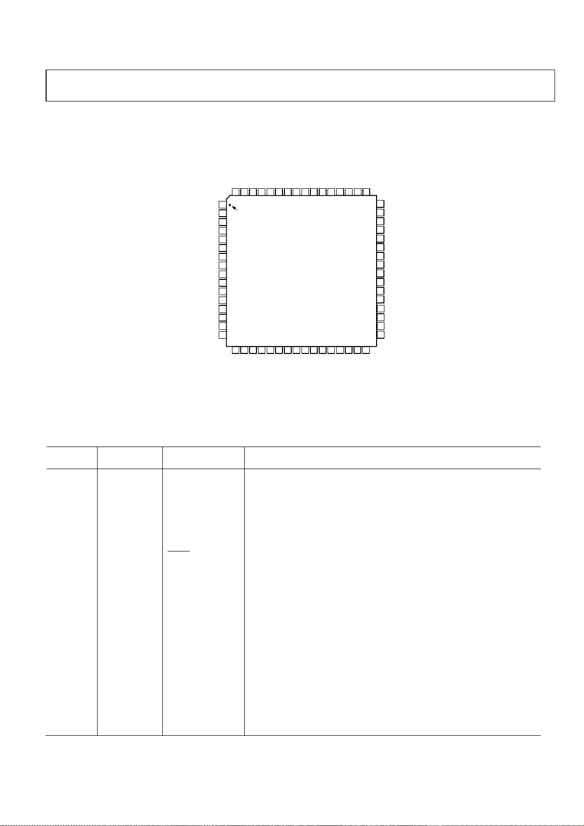
PIN CONFIGURATION AND FUNCTION DESCRIPTIONS
N
P
N
P
L
R
R
L
D
T
T
T
T
D
N
U
U
U
U
D
G
V
O
O
O
O
V
V
V
V
A
A
48
ADVDD
47
ADGND
46
PLL_LF2
45
PLL_LF1
44
PLL_GND
43
PLL_VDD
42
DGND
41
SYSCLK1
40
SYSCLK2
39
SYSCLK3
38
XIN
37
XOUT
36
MCLKO
35
MCLKI
34
DVDD
33
DGND
29
30
32
31
28
A
K
K
K
K
L
L
C
C
R
B
L
X
X
U
U
A
A
O
O
A
T
L
L
T
A
C
C
A
D
R
B
D
L
S
X
S
X
X
X
U
U
U
U
A
I
A
A
A
I
I
O
5
4
0
0
2
0
8
VINR
VINL
AGND
AVDD
DIR_LF
DIR_GND
DIR_VDD
RESET
CLATCH/AD0
CIN/SDA
CCLK/SCL
COUT/AD1
ZEROL/INT
ZEROR
DVDD
DGND
P
N
L
P
A
C
64 63 62 61 60 59 58
1
PIN 1
2
IDENTIFIER
3
4
5
6
7
8
9
10
11
12
13
14
15
16
17 18 19 20 21 22 23 24
K
L
C
R
L
I
N
P
D
L
N
P
A
G
C
A
A
K
T
L
A
C
D
B
I
S
I
R
P
A
C
K
L
C
R
L
O
D
R
P
A
C
K
L
C
B
O
D
D
D
V
A
(Not to Scale)
A
T
A
D
S
O
D
F
N
T
N
E
L
G
G
R
I
A
V
A
F
57 56 55 54 53 52 51 50 49
ADAV802
TOP VIEW
25 26
T
D
N
D
I
U
D
N
R
I
V
O
G
D
T
D
D
I
O
O
D
27
Figure 2. 64-Lead Plastic Quad Flatpack [LQFP] (ST-520)
Table 18. ADAV802 Pin Function Descriptions
Pin
Number Input/Output Mnemonic Description
1 INPUT VINR Analog Audio Input - Right Channel
2 INPUT VINL Analog Audio Input - Left Channel
3 AGND Analog Ground
4 AVDD Analog Voltage Supply
5 DIR_LF DIR Phase Locked Loop (PLL) Loop Filter Pin
6 DIR_GND Supply Ground for DIR Analog Section. This pin should be connected to AGND
7 DIR_VDD Supply for DIR Analog Section. This pin should be connected to AVDD
8 INPUT
RESET
Reset input (Active Low)
9 INPUT CLATCH Chip Select (Control Latch) Pin of SPI compatible control interface
10 INPUT CIN Data Input of SPI compatible control interface
11 INPUT CCLK Clock Input of SPI compatible control interface
12 OUTPUT COUT Data Output of SPI compatible control interface
13 OUTPUT ZEROL/INT
Left Channel (Output) Zero Flag or Interrupt (Output) Flag. The function of this
pin is determined by the INTRPT bin in DAC Control Register 4
14 OUTPUT ZEROR Right Channel (Output) Zero Flag
15 DVDD Digital Voltage Supply
16 DGND Digital Ground
17 INPUT/OUTPUT ILRCLK Sampling Clock (LRCLK) of Playback Digital Input Port
18 INPUT/OUTPUT IBCLK Serial Clock (BCLK) of Playback Digital Input Port
19 INPUT ISDATA Data Input of Playback Digital Input Port
20 INPUT/OUTPUT OLRCLK Sampling Clock (LRCLK) of Record Digital Output Port
21 INPUT/OUTPUT OBCLK Serial Clock (BCLK) of Record Digital Output Port
22 OUTPUT OSDATA Data Output of Record Digital Output Port
Rev. Pr G | Page 9 of 53

ADAV802 Preliminary Technical Data
Pin
Number Input/Output Mnemonic Description
23 INPUT DIRIN Input to Digital Input Receiver (S/PDIF)
24 ODVDD Interface Digital Voltage Supply
25 ODGND Interface Digital Ground
26 OUTPUT DITOUT S/PDIF Output from DIT
27 INPUT/OUTPUT OAUXLRCLK Sampling Clock (LRCLK) of Auxiliary Digital Output Port
28 INPUT/OUTPUT OAUXBCLK Serial Clock (BCLK) of Auxiliary Digital Output Port
29 OUTPUT OAUXSDATA Data Output of Auxiliary Digital Output Port
30 INPUT/OUTPUT IAUXLRCLK Sampling Clock (LRCLK) of Auxiliary Digital Input Port
31 INPUT/OUTPUT IAUXBCLK Serial (BCLK) of Auxiliary Digital Input Port
32 INPUT IAUXSDATA Data Input of Auxiliary Digital Input Port
33 DGND Digital Ground
34 DVDD Digital Supply Voltage
35 INPUT MCLKI External MCLK Input
36 OUTPUT MCLKO Oscillator Output
37 INPUT XOUT Crystal Input
38 INPUT XIN Crystal or External MCLK Input
39 OUTPUT SYSCLK3 System Clock 3 (from PLL 2)
40 OUTPUT SYSCLK2 System Clock 2 (from PLL 2)
41 OUTPUT SYSCLK1 System Clock 1 (from PLL 1)
42 DGND Digital Ground
43 PLL_VDD Supply for PLL Analog Section. This pin should be connected to AVDD
44 PLL_GND Ground for PLL Analog Section. This pin should be connected to AGND
45 PLL_LF1 Loop Filter for PLL1
46 PLL_LF2 Loop Filter for PLL2
47 ADGND Analog Ground (Mixed Signal)
48 ADVDD Analog Voltage Supply (Mixed Signal). This pin should be connected to AVDD
49 OUTPUT VOUTRP Right Channel Differential Analog Output (Positive)
50 OUTPUT VOUTRN Right Channel Differential Analog Output (Negative)
51 OUTPUT VOUTLP Left Channel Differential Analog Output (Positive)
52 OUTPUT VOUTLN Left Channel Differential Analog Output (Negative)
53 AVDD Analog Voltage Supply
54 AGND Analog Ground
55 FILTD Output DAC Reference Decoupling
56 AGND Analog Ground
57 VREF Voltage Reference Voltage
58 AGND Analog Ground
59 AVDD Analog Voltage Supply
60 CAPRN ADC Modulator Input Filter Capacitor (Right Channel - Negative)
61 CAPRP ADC Modulator Input Filter Capacitor (Right Channel - Positive)
62 AGND Analog Ground
63 CAPLP ADC Modulator Input Filter Capacitor (Left Channel - Positive)
64 CAPLN ADC Modulator Input Filter Capacitor (Left Channel - Negative)
Rev. Pr G | Page 10 of 53

Preliminary Technical Data ADAV802
(continued from Page 1)
Operation of the ADAV802 is controlled via an SPI compatible
serial interface which allows individual Control Register
settings to be programmed. The ADAV802 operates from a
single analog +3.3 V power supply - and a digital power supply
of +3.3 V with optional digital interface range of 3.0 V to +3.6 V.
It is housed in a 64-lead LQFP package and is characterized for
operation over the commercial temperature range −40°C to
85°C.
Rev. Pr G | Page 11 of 53
ADAV802 Preliminary Technical Data
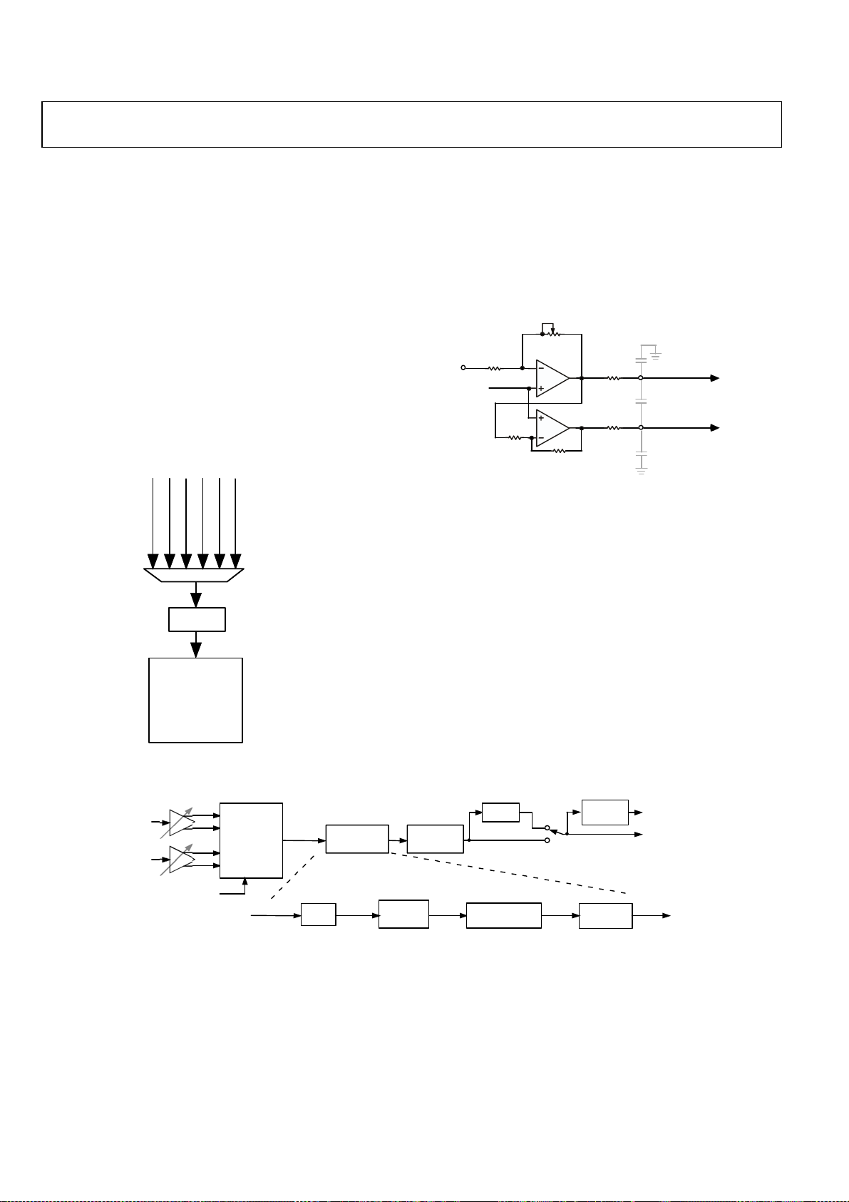
FUNCTIONAL DESCRIPTION
ADC SECTION
The ADAV802's ADC section is implemented using a 2nd order
multi-bit (5-bits) Sigma-Delta modulator. The modulator is
sampled at either half the ADC MCLK rate (Modulator Clock =
128 × f
) or a quarter of the ADC MCLK rate (Modulator Clock
S
= 64 × f
followed by a cascade of 3 half-band FIR filters. The Sinc
decimates by a factor of 16 at 48 kHz and by 8 at 96 kHz. Each
of the half-band filters decimates by a factor of 2. Figure 3 below
shows the detail of the ADC section. The ADC can be clocked
by a number of different clock sources to control the sample
rate. MCLK selection for the ADC is set by Internal Clocking
Control Register 1 (address = 0x76). The ADC provides an
output word of up to 24 bits in resolution in 2s complement
format. The output word can be routed to the output ports, to
the sample rate converter or to the SPDIF digital transmitter.
). The digital decimator consists of a Sinc^5 filter
S
DIR PLL(512 × f
DIR PLL(256 × f
S
)
PLL2 INTERNAL
S
)
ADC MCLK
DIVIDER
PLL1 INTERNAL
MCLKI
XIN
REG:0x6F
BITS 1-0
REG: 0x76
BITS4-2
Programmable Gain Amplifier (PGA)
The input of the record channel features a PGA which converts
the single-ended signal to a differential signal which is applied
to the analog sigma-delta modulator of the ADC. The PGA can
be programmed to amplify a signal by up to 24dB in 0.5dB
increments. Figure 4 details the structure of the PGA circuit.
4-64kΩ
External
Capacitor
8kΩ
(1nFNPO)
125Ω
125Ω
External
Capacitor
(1nF NPO)
CAPxN
External
Capacitor
(1nF NPO)
CAPxP
To
Modulator
5
0
0
0
1
0
8
4kΩ
VREF
8kΩ
Figure 4. PGA Block Diagram
Analog Sigma Delta Modulator
The ADC features a 2nd order, multi-bit, Sigma-Delta modulator.
The input features two integrators in cascade followed by a flash
converter. This multi-bit output is directed to a scrambler,
followed by a DAC for loop feedback. The Flash ADC output is
also converted from "thermometer" coding to "binary" coding
for input as a 5-bit word to the decimator. Figure 5 shows the
ADC block diagram.
ADC
MCLK
ADC
4
0
0
0
-
1
0
8
Figure 3. Clock Path Control on the ADC
MULTI-BI T
SIGMA-DELTA
MODULATOR
ADC MODCLK
ADC M CLK/2
(TYP 6.144MHz)
CONTROL
HALFBAND
FILTER
VOLUM E
SINC^5
DECIMATOR
384kHz
768kHz
Figure 5. ADC Block Diagram
The ADC also features independent digital volume control for
the left and right channels. The volume control consists of 256
linear steps with each step reducing the digital output codes by
0.39%. Each channel also has a peak detector which records the
peak level of the input signal. The peak detector register is
cleared by reading it.
PEAK
DETECT
HALFBAND
FILTER
801-0003
48kHz
96kHz
192kHz
384kHz
HPF
SINC
COMPENSATION
96kHz
192kHz
Rev. Pr G | Page 12 of 53

Preliminary Technical Data ADAV802
Selecting A Sample Rate
The sample rate of the ADC is always 256 × f
. To facilitate
S
different MCLKs the ADC block has a programmable divider
which allows the MCLK to be divided by 1, 2 or 3 before being
applied to the ADC. This allows for MCLKs of 256 × f
, 512 × f
S
or 768 × fS to be applied to the ADC. To synchronize the data
output port with the ADC the same divider setting should be
applied to the Internal Clock (ICLK1 or ICLK2) which is
controlling the output port. The Internal Clock dividers are
shown in Figure 34. By default the ∑∆ modulator runs at ADC
MCLK/2. The modulator is designed to run with a maximum
clock rate of 6.144MHz,. For cases where higher sample rates
would run the modulator at speeds higher than this the user can
select divide the ADC MCLK by 4 before it is applied to the
modulator. To compensate for this the modulator uses an
alternate filter configuration. The divide setting is selected by
the AMC bit in ADC Control Register 1.
Automatic Level Control (ALC)
The ADC record channel features a programmable automatic
level control block. This block monitors the level of the ADC
output signal and will automatically reduce the gain if the signal
at the input pins causes the ADC output to exceed a preset limit.
This function can be useful to maximize the signal dynamic
range when the input level is not well-defined. The PGA can be
used to amplify the unknown signal and the ALC will reduce
the gain until the ADC output is within the preset limits. This
results in maximum front-end gain. Since the ALC block
monitors the output of the ADC the volume control function
should not be used. The ADC volume control scales the results
from the ADC and any distortion caused by the input signal
exceeding the input range of the ADC will still be present at the
output of the ADC but scaled by a value determined by the
volume control register. The ALC block consists of two
functions, Attack Mode and Recovery Mode. The Recovery
Mode consists of three settings, namely, No Recovery, Normal
Recovery and Limited Recovery. Each of these modes in
discussed in detail below. Figure 6 shows an overall flow
diagram of the ALC block.
Attack Mode
When the absolute value of the ADC output exceeds the level
set by the Attack Threshold bits in the ALC Control Register 2,
Attack Mode is initiated. The PGA gain for both channels is
reduced by one step (0.5dB). The ALC will then wait for a time
determined by the Attack Timer bits before sampling the ADC
output value again. If the ADC output is still above the
threshold the PGA gain is reduced by a further step. This
procedure continues until the ADC output is below the limit set
by the Attack Threshold bits. The initial gains of the PGAs are
defined by ADC Left PGA Gain Register and ADC Right PGA
Gain Register and may be different values. The ALC simply
adds or subtracts a common gain offset to these values. The
S
ALC will preserve any gain difference in dB as defined by those
registers. At no time will the PGA gains exceed their initial
values. Therefore, the initial gain setting also serves as a
maximum value.
The Limit Detection Mode bit in ALC Control Register 1
determines how the ALC should respond to an ADC output
which exceeds the set limits. If this bit is a one then both
channels must exceed the threshold before the gain is reduced.
This mode can be used to prevent unnecessary gain reduction
due to spurious noise on a single channel. If the Limit Detection
Mode bit is a zero the gain will be reduced when either channel
exceeds the threshold.
No Recovery Mode
By default there is no gain recovery. Once the gain has been
reduced it will not be recovered until the ALC has been reset, by
toggling the ALCEN bit in ALC Control Register 1 or by writing
any value to ALC Control Register 3. The latter option is more
efficient as it requires only one write operation to reset the ALC
function. No Recovery Mode prevents volume modulation of
the signal, caused by adjusting the gain, which can create
undesirable artifacts in the signal. Since the gain can be reduced
but not recovered, care should be taken that spurious signals do
not interfere with the input signal as these may trigger a gain
reduction unnecessarily.
Normal Recovery
This mode allows for the PGA gain to be recovered providing
that the input signal meets certain criteria. Firstly, the ALC must
not be in Atta ck Mode, i.e., the PGA gain ha s been reduced
sufficiently such that the input signal is below the level set by
the Attack Threshold bits. Secondly, the output result from the
ADC must be below the level set by the Recovery Threshold bits
in ALC Control Register. If both of these criteria are met the
gain is recovered by one step (0.5dB). The gain is incrementally
restored to its original value assuming the ADC output level is
below the Recovery Threshold at intervals determined by the
Recovery Time bits. Should the ADC output level exceed the
Recovery Threshold while the PGA gain is being restored the
PGA gain value will be held and will not continue restoration
until the ADC output level is again below the Recovery
Threshold. Once the PGA gain is restored to its original value it
will not be changed again unless the ADC output value exceeds
the Attack Threshold and the ALC then enters Attack Mode.
Care should be exercised when using this mode to choose
values for the Attack and Recovery thresholds to prevent
excessive volume modulation caused by continuous gain
adjustments.
Limited Recovery
Limited Recovery Mode offers a compromise between No
Rev. Pr G | Page 13 of 53
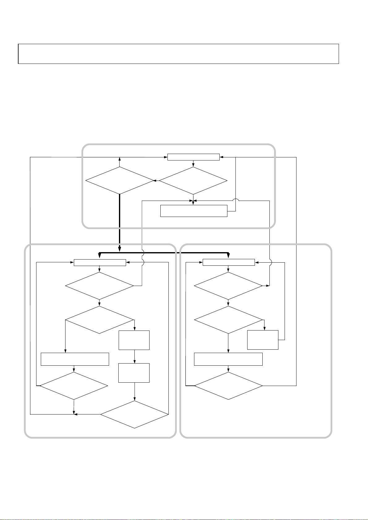
ADAV802 Preliminary Technical Data
Recovery and Normal Recovery Modes. If the output level of
the ADC exceeds the Attack Threshold then Attack Mode is
initiated. When Attack Mode has reduced the PGA gain to
suitable levels the ALC will attempt to recovery the gain to its
original level. If the ADC output level exceeds the level set by
the Recovery Threshold bits a counter is incremented
(GAINCNTR). This counter is incremented, at intervals equal
ATTACK MODE
NO
to the Recovery Time selection, if the ADC has any excursion
above the Recovery Threshold. If the counter reaches its
maximum value, determined by the GAINCNTR bits in ALC
Control Register 1, the PGA gain is deemed suitable and no
further gain recovery is attempted. If, at any time, the ADC
output level exceeds the Attack Threshold, Attack Mode is
reinitiated and the counter is reset
WAIT FOR SAMPLE
LIMITED RECOVERY
WAIT FOR SAMPLE
IS SAMPLE
ABOVE ATTACK
THRESHOLD?
YES
IS SAMPLE
BELOW RECOVERY
THRESHOLD?
IS A RECOVERY
MODE ENABLED?
NO
YES
NO
WAIT
RECOVERY
TIME
NO
IS SAMPLE
GREATER THAN ATTACK
THRESHOLD?
YES
DECREASE GAIN BY 0 .5dB
AND WAIT ATTACK TIME
NORMAL RECOVERY
WAIT FOR SAMPLE
IS SAMPLE
ABOVE ATTACK
THRESHOLD?
NO
IS SAMPLE
BELOW RECOVERY
THRESHOLD?
YES
NO
WAIT
RECOVERY
TIME
INCREASE GAIN BY 0.5dB
WAIT RECOVERY TIME
HAS GAIN BEEN
FULLY RESTORED?
NO
YES
INCREMENT
GAINCNTR
IS GA INCNTR
AT MAXIMUM?
NOYES
INCREASE GAIN BY 0.5dB
WAIT RECOVERY TIME
HAS GAIN BEEN
FULLY RESTORED?
NO
YES
7
2
1
0
1
0
8
Figure 6. ALC Flow Diagram
Rev. Pr G | Page 14 of 53
Preliminary Technical Data ADAV802
DAC SECTION
The ADAV802 has two DAC channels arranged as a stereo pair
with differential analog outputs. Each channel has its own
independently programmable attenuator, adjustable in 128 steps
of 0.375dB per step. The DAC can receive data from the
playback or auxiliary input ports, the SRC, the ADC or the DIR.
Each analog output pin sits at a dc level of VREF, and swings 1.0
Vrms for a 0dB digital input signal. A single op-amp third-order
external low-pass filter is recommended to remove highfrequency noise present on the output pins. Note that the use of
op amps with low slew rate or low bandwidth may cause high
frequency noise and tones to fold down into the audio band;
care should be exercised in selecting these components. The
FILTD and FILTR pins should be bypassed by external
capacitors to AGND. The FILTD pin is used to reduce the noise
of the internal DAC bias circuitry, thereby reducing the DAC
output noise. The voltage at the VREF pin, FILTR can be used to
bias external op amps used to filter the output signals. For
applications where the FILTR is required to drive external op
amps which may draw more than 50µA or may have dynamic
load changes extra buffering should be used to preserve the
quality of the ADAV802 reference. The digital input data source
for the DAC can be selected from a number of available sources.
by programming the appropriate bits in the Datapath Control
register. Figure 7 shows how the digital data source and MCLK
source for the DAC are selected. Each DAC has an independent
volume register giving 256 steps of control with each step giving
approximately 0.375dB of attenuation. Each DAC also has a
peak level register which records the peak value of the digital
audio data. Reading the register clears the peak .
DAC
ANALOG
OUTPUT
DAC
MULTI-BI T
SIGMA-DELTA
MODULATO R
TO ZERO FLAG PINS
Figure 8. DAC Block Diagram
TO CONTROL
INTERPOLATOR
Selecting a Sample Rate
Correct operation of the DAC is dependant upon the data rate
provided to the DAC, the master clock applied to the DAC and
the selected interpolation rate. By default the DAC assumes that
the MCLK rate is 256 times the sample rate which requires an 8
times oversampling rate. This combination is suitable for
sample rates up to 48kHz. For the case of a 96kHz data rate
which has a 24.576MHz MCLK (256 × f
) associated with it the
S
DAC MCLK divider should be set to divide the MCLK by 2.
This will prevent the DAC engine being run too fast. To
compensate for the reduced MCLK rate the interpolator should
be selected to operate in 4 × (DAC MCLK = 128 × f
combinations can be selected for different sample rates.
DIR PLL(256 × f
DIR PLL(512 × f
PLL1 INTERNAL
PLL2 INTERNAL
MCLKI
XIN
REG: 0x76
BITS 7-5
REG:0x65
BITS 3-2
DAC
INPUT
FROM DAC
DATAPATH
MULTIPLEXER
REG: 0x63
BITS 5-3
AUXILIARY IN
PLAYBACK
DIR
ADC
REGISTERS
S
S
)
)
MCLK
DIVIDER
DAC
MCLK
DAC
801-0007
Figure 7. Clock and data Path Control on the DAC
PEAK
DETECTOR
VOLUME/MUTE
CONTROL
ZERO DETECT
801-0006
). Similar
S
Rev. Pr G | Page 15 of 53
ADAV802 Preliminary Technical Data
f
S_OUT
9
0
0
0
-
1
0
8
S_IN
= 192
OUT
× 220.
SRC FUNCTIONAL OVERVIEW
THEORY OF OPERATION
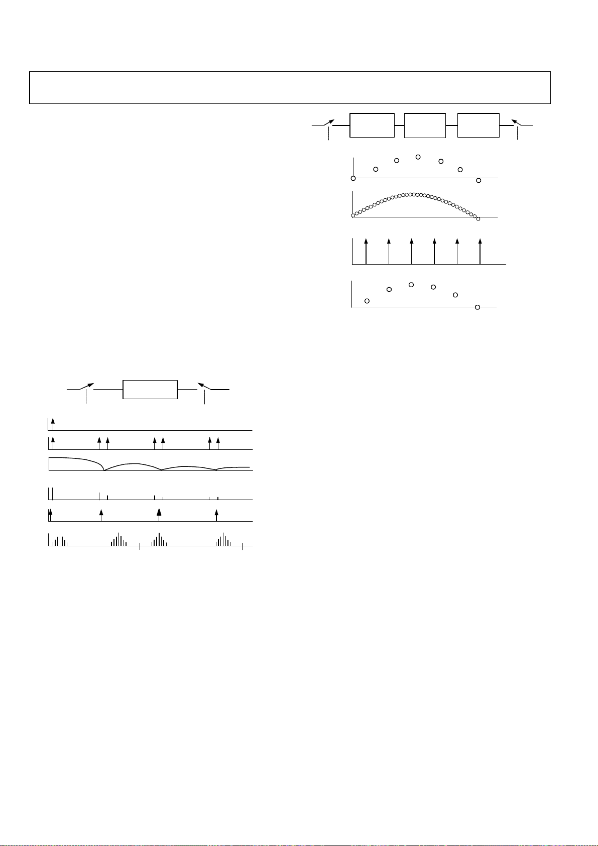
Asynchronous sample rate conversion is converting data from
at the same or different sample rate. The simplest approach to
an asynchronous sample rate conversion is the use of a zeroorder hold between the two samplers shown in Figure 9 In an
asynchronous system, T2 is never equal to T1 nor is the ratio
between T2 and T1 rational. As a result, samples at fS_OUT will
be repeated or dropped producing an error in the re-sampling
process. The frequency domain shows the wide side lobes that
result from this error when the sampling of fS_OUT is
convolved with the attenuated images from the sin(x)/x nature
of the zero-order hold. The images at fS_IN, dc signal images, of
the zero-order holdare infinitely attenuated. Since the ratio of
T2 to T1 is an irrational number, the error resulting from the resampling at fS_OUT can never be eliminated. However, the
error can be significantly reduced through interpolation of the
input data at fS_IN. The sample rate converter in the ADAV802
is conceptually interpolated by a factor of 2
IN
f
=1/T1
S_IN
SPECTRUM OF ZERO-ORDER HOLD OUTPUT
ZERO-ORDER
HOLD
ORIGINAL SIGNAL
SAMPLED AT f
SIN(X)/X OF ZER0-ORDER HOLD
S_IN
f
S_OUT
20
.
OUT
=1/T2
IN
INTERPOLATE
BY N
f
S_IN
TIME DOMAIN OF f
TIME DOMAIN OUTPUT OF THE LOW-PASS FILTER
TIME DOMAIN OF f
TIME DOMAIN OF THE ZERO-ORDER HOLD OUTPUT
LOW-P ASS
S_IN
S_OUT
FILTER
SAMPLES
RESAMPLING
ZERO-ORDER
HOLD
Figure 10. SRC Time Domain
In the frequency domain shown in Figure 11, the interpolation
expands the frequency axis of the zero-order hold. The images
from the interpolation can be sufficiently attenuated by a good
low-pass filter. The images from the zero-order hold are now
pushed by a factor of 2
of the zero-order hold, which is f
20
closer to the infinite attenuation point
× 220 The images at the
S_IN
zero-order hold are the determining factor for the fidelity of the
output at f
. The worst-case images can be computed from
S_OUT
the zero-order hold frequency response, maximum image = sin
(× F/f
image that would be 2
The following worst-case images would appear for f
S_INTERP
)/(× F/f
). F is the frequency of the worst-case
S_INTERP
20
× f
± f
S_IN
/2 , and f
S_IN
S_INTERP
is f
S_IN
kHz:
SPECTRUMOF f
f
S_OUT
FREQUENCY RESPONSE OF fS_OUT CONVOL VED WITH ZERO-ORDER
HOLD SPECTRUM
S_OUT
SAMPLING
2 × f
S_OUT
801-0008
Figure 9. Zero Order Hold Being Used by fS OUT to Resample Data from fS_IN
CONCEPTUAL HIGH INTERPOLATION MODEL
Interpolation of the input data by a factor of 220 involves placing
20
(2
−1) samples between each f
both the time domain and the frequency domain of
interpolation by a factor of 2
20
2
would involve the steps of zero-stuffing (220 −1) number of
samples between each f
S_IN
interpolated signal with a digital low-pass filter to suppress the
images. In the time domain, it can be seen that f
closest f
the nearest f
× 220 sample from the zero-order hold as opposed to
S_IN
sample in the case of no interpolation. This
S_IN
significantly reduces the re-sampling error.
sample. Figure 10 shows
S_IN
20
. Conceptually, interpolation by
sample and convolving this
selects the
S_OUT
Rev. Pr G | Page 16 of 53
Image at f
Image at f
− 96 kHz = –125.1 dB
S_INTERP
+ 96 kHz = –125.1 dB
S_INTERP

Preliminary Technical Data ADAV802
T
IN OUT
INTERPOLATE
BY N
f
S_IN
FREQUENCY DOMAIN OF SAMPLES AT f
FREQUENCY DOMAIN OF THE INTERPOLATION
SIN(X)/X OF ZER0-ORDER HOLD
FREQUENCY DOMAIN OF f
FREQUENCY DOMAIN AFTER
RESAMPLING
LOW-P ASS
FILTER
S_OUT
RESAMPLING
S_IN
220× f
ZERO-ORDER
HOLD
f
S_IN
220× f
S_IN
220× f
S_IN
S_IN
f
S_OUT
0
1
0
0
-
1
0
8
Figure 11. Frequency Domain of the Interpolation and Resampling
HARDWARE MODEL
The output rate of the low-pass filter of Figure 10 would be the
interpolation rate, 2
rate of 201.3 GHz is clearly impractical, not to mention the
number of taps required to calculate each interpolated sample.
However, since interpolation by 2
samples between each f
low-pass FIR filter are by zero. A further reduction can be
realized by the fact that since only one interpolated sample is
taken at the output at the f
to be performed per f
64-tap FIR filter for each f
the images caused by the interpolation. The difficulty with the
above approach is that the correct interpolated sample needs to
be selected upon the arrival of f
convolutions per f
must be measured with an accuracy of 1/201.3 GHz = 4.96 ps.
Measuring the f
frequency is clearly impossible; instead, several coarse
measurements of the f
over time.
Another difficulty with the above approach is the number of
coefficients required. Since there are 2
with a 64-tap FIR filter, there needs to be 2
coefficients for each tap, which requires a total of 2
coefficients. To reduce the amount of coefficients in ROM, the
SRC stores small subset of coefficients and performs a high
order interpolation between the stored coefficients. So far the
above approach works for the case of f
the case when the output sample rate, f
input sample rate, f
20
× 192000 kHz = 201.3 GHz. Sampling at a
20
involves zero-stuffing 220−1
sample, most of the multiplies in the
S_IN
rate, only one convolution needs
S_OUT
period instead of 220 convolutions. A
S_OUT
sample is sufficient to suppress
S_OUT
. Since there are 220 possible
S_OUT
period, the arrival of the f
S_OUT
period with a clock of 201.3 GHz
S_OUT
clock period are made and averaged
S_OUT
20
possible convolutions
S_OUT
S_OUT
, the ROM starting address, input data,
S_IN
S_OUT
20
polyphase
26
> f
. However, in
S_IN
, is less than the
clock
and the length of the convolution must be scaled. As the input
sample rate rises over the output sample rate, the anti-aliasing
filter’s cutoff frequency has to be lowered because the Nyquist
frequency of the output samples is less than the Nyquist
frequency of the input samples. To move the cutoff frequency of
the antialiasing filter, the coefficients are dynamically altered
and the length of the convolution is increased by a factor of
(f
S_IN/fS_OUT
).
This technique is supported by the Fourier transform property
that if f(t) is F(ω), then f(k × t) is F(ω/k). Thus, the range of
decimation is simply limited by the size of the RAM.
THE SAMPLE RATE CONVERTER ARCHITECTURE
The architecture of the sample rate converter is shown in Figure
12. The sample rate converter’s FIFO block adjusts the left and
right input samples and stores them for the FIR filter’s
convolution cycle. The f
to the FIFO block and the ramp input to the digital servo loop.
The ROM stores the coefficients for the FIR filter convolution
and performs a high order interpolation between the stored
coefficients. The sample rate ratio block measures the sample
rate for dynamically altering the ROM coefficients and scaling
of the FIR filter length as well as the input data. The digital
servo loop automatically tracks the f
and provides the RAM and ROM start addresses for the start of
the FIR filter convolution.
RIGHT DATA IN
LEFTDATAIN FIFO
f
S_IN
COUNTER
f
S_IN
f
S_OUT
Figure 12. Architecture of the Sample Rate Converter
The FIFO receives the left and right input data and adjusts the
amplitude of the data for both the soft muting of the sample
rate converter and the scaling of the input data by the sample
rate ratio before storing the samples in the RAM. The input data
is scaled by the sample rate ratio because as the FIR filter length
of the convolution increases, so does the amplitude of the
convolution output. To keep the output of the FIR filter from
saturating, the input data is scaled down by multiplying it by
(f
S_OUT/fS_IN
) when f
data for muting and unmuting of the SRC.
The RAM in the FIFO is 512 words deep for both left and right
channels. An offset to the write address provided by the f
counter is added to prevent the RAM read pointer from ever
overlapping the write address. The minimum offset on the SRC
counter provides the write address
S_IN
and f
S_IN
ROM A
ROM B
ROM C
ROM D
DIGITAL
SERVO LOOP
SAMPLE RATERAT IO
SAMPLE RATE
RATIO
< f
S_OUT
. The FIFO also scales the input
S_IN
EXTERNAL
RATIO
FIR FILTER
sample rates
S_OUT
ORDER
INTERP
L/R DATA OU
HIGH
801-0011
S_IN
Rev. Pr G | Page 17 of 53

ADAV802 Preliminary Technical Data
is 16 samples. However, the Group Delay and Mute In register
can be used to increase this offset. The number of input samples
added to the write pointer of the FIFO on the SRC is 16 + Bits
6-0 of the Group Delay register. This feature is useful in varispeed applications in order to prevent the read pointer to the
FIFO running ahead of the write pointer. When set, bit 7 of the
Group Delay and Mute In register will soft mute the sample
rate. Increasing the offset of the write address pointer is useful
for applications when small changes in the sample rate ratio
between f
S_IN
and f
are expected. The maximum decimation
S_OUT
rate can be calculated from the RAM word depth and the group
delay as (512−16)/64 taps = 7.75 for short group delay and (512-
64)/64 taps = 7 for long group delay.
The digital servo loop is essentially a ramp filter that provides
the initial pointer to the address in RAM and ROM for the start
of the FIR convolution. The RAM pointer is the integer output
of the ramp filter while the ROM is the fractional part. The
digital servo loop must be able to provide excellent rejection of
jitter on the f
of the f
S_OUT
S_IN
and f
clocks as well as measure the arrival
S_OUT
clock within 4.97 ps. The digital servo loop will also
divide the fractional part of the ramp output by the ratio of
f
S_IN/fS_OUT
for the case when f
S_IN
> f
, to dynamically alter
S_OUT
the ROM coefficients.
The digital servo loop is implemented with a multi-rate filter. To
settle the digital servo loop filter more quickly upon startup or a
change in the sample rate, a “fast mode” was added to the filter.
When the digital servo loop starts up or the sample rate is
changed, the digital servo loop kicks into “fast mode” to adjust
and settle on the new sample rate. Upon sensing the digital
servo loop settling down to some reasonable value, the digital
servo loop will kick into “normal” or “slow mode.”
During “fast mode” the MUTE_OUT bit in the Sample Rate
Error register is asserted to let the user know clicks or pops may
be present in the digital audio data. The output of the SRC can
be muted, by asserting bit 7 of the Group Delay & Mute register
until the SRC has changed to “slow mode”. The MUTE_OUT bit
can be set to generate an interrupt when the SRC changes to
“slow mode” indicating that the data will be sample rate
converted accurately. The frequency response of the digital
servo loop for "fast mode" and "slow mode" are shown in Figure
14. The FIR filter is a 64-tap filter in the case of f
is (f
S_IN/fS_OUT
) × 64 taps for the case when f
S_IN
> f
S_OUT
S_OUT
≥ f
and
S_IN
. The FIR
filter performs its convolution by loading in the starting address
of the RAM address pointer and the ROM address pointer from
the digital servo loop at the start of the f
period. The FIR
S_OUT
filter then steps through the RAM by decrementing its address
by 1 for each tap, and the ROM pointer increments its address
by the (f
f
. Once the ROM address rolls over, the convolution is
S_IN
S_OU
T/f
) × 220 ratio for f
S_IN
S_IN
> f
S_OUT
or 220 for f
S_OUT
≥
completed. The convolution is performed for both the left and
right channels, and the multiply accumulate circuit used for the
convolution is shared between the channels. The f
S_IN/fS_OUT
sample rate ratio circuit is used to dynamically alter the
>f
coefficients in the ROM for the case when f
is calculated by comparing the output of an f
output of an f
If f
> f
S_IN
by more than two f
counter. If f
S_IN
, the sample rate ratio is updated if it is different
S_OUT
periods from the previous f
S_OUT
S_OUT
>f
the ratio is held at one.
S_IN,
S_IN
S_OUT
. The ratio
S_OUT
counter to the
to f
S_OUT
S_IN
comparison. This is done to provide some hysteresis to prevent
the filter length from oscillating and causing distortion.
PLLINT2
PLLINT1
REG: 0x76
BIT 1
2
1
0
0
1
0
8
DIR PLL (512 × f
S
)
MCLK
SRC
OUTPUT
DIR PLL (256 × f
S
)
SRC
SRC
ICLK2
XIN
ICLK1
REG:0x00
BITS 1-0
SRC
INPUT
MCLKI
REG:0x76
BIT 0
REG: 0x62
BITS 7-6
AUXILIARY IN
PLAYBACK
DIR
ADC
Figure 13. Clock and Data Path Control on the SRC
10
0
-10
-20
-30
-40
-50
-60
-70
-80
B
-90
d
E
-100
D
U
-110
T
I
N
-120
G
A
M
-130
-140
-150
-160
-170
-180
-190
-200
-210
-220
0.01
SLOWMODE
0.1 1 10 100 1e3 1e4 1e5
FREQUENCY - Hz
FAST MO DE
3
1
0
0
1
0
8
Figure 14. Frequency Response of the Digital Servo Loop. fS_IN is the X-Axis,
fS_OUT = 192 KHz, Master Clock is 30 MHz
PLL SECTION
The ADAV802 features a dual PLL configuration to generate
independent system clocks for asynchronous operation. Figure
17 shows the block diagram of the PLL section. The PLL
generates the internal and system clocks from a 27MHz clock.
This clock is generated either by a crystal connected between
XIN and XOUT, as shown in Figure 15 or from an external
Rev. Pr G | Page 18 of 53

Preliminary Technical Data ADAV802
A
clock source connected directly to XIN. A 54MHz clock can
also be used if the internal clock divider is used. Both PLLs
(PLL1 and PLL2) can be programmed independently and cater
for a range of sampling rates (32/44.1/48 kHz) with selectable
system clock oversampling rates of 256 and 384. Higher
oversampling rates can also be selected by enabling the
doubling of the sampling rate to give 512 or 768 × f
ratios. Note
S
that this option also allows oversampling ratios of 256 or 384 at
double sample rates of 64/88.2/96 kHz. The PLL outputs can be
routed internally to act as clock sources for the other
component blocks such as the ADC, DAC etc. The outputs of
the PLLs are also available on the three SYSCLK pins. Figure 18
shows how the PLLs can be configured to provide the sampling
clocks.
L
XT
C
N
I
X
Figure 15. Crystal Connection
C
T
U
O
7
X
1
0
0
1
0
8
Table 19. PLL Frequency Selection Options
PLL Sample Rate MCLK Selection
(fS) Normal fS Double fS
1 32/44.1/48 kHz 256/384×fS 512/768×fS
64/88.2/96 kHz 256/384×fS
2A 32/44.1/48 kHz 256/384×fS 512/768×fS
64/88.2/96 kHz 256/384×fS
2B Same as fS selected 512×fS
for PLL 2A 512×fS
The PLLs require a some external components to operate
correctly. These components, shown in Figure 16 form a loop
filter which integrates the current pulses from a charge pump
and produces a voltage which is used to tune the VCO. Good
quality capacitors, such as PPS film, are recommended .Figure
17 shows a block diagram of the PLL section including master
clock selection. Figure 18 shows how the clock frequencies at
the clock output pins, SYSCLK1-3 and the internal PLL clock
values, PLL1 and PLL2 are selected. The clock nodes, PLL1 and
PLL2, can be used as master clocks for the other blocks in the
ADAV802 such as the DAC or ADC. The PLL has separate
supply and ground pins and these should be as clean as possible
to prevent electrical noise being converted into clock jitter by
coupling onto the loop filter pins.
XIN
XOUT
MCLKO
MCLKI
801-0015
REG: 0x74
BIT 5
AVDD
1.8nF
33nF
732Ω
Figure 16. PLL L
PLL_L F1
REG: 0x78
/2
REG: 0x74
BIT 4
/2
BIT 6
REG: 0x78
BIT 7
PHASE
DETECTOR
&LOOP
FILTER
PHASE
DETECTOR
&LOOP
FILTER
PLL_LF2
VCO
N DIVIDER
VCO
N DIVIDER
OUTPUT
SCALER N1
OUTPUT
SCALER N2
OUTPUT
SCALER N3
PLL1
PLL2
Figure 17. PLL Section Block Diagram
BLOCK
PLL_LFx
F
SYSCLK1
SYSCLK2
SYSCLK3
PLL
4
1
0
0
1
0
8
Rev. Pr G | Page 19 of 53

ADAV802 Preliminary Technical Data
48 kHz
32 kHz
44.1 kHz
256
384
256
384
48 kHz
32 kHz
44.1 kHz
256
512
PLL1 MCLK
PLL2 MCLK
REG: 0x75
BITS 3-2
REG: 0x75
BIT 1
REG: 0x75
BIT 5
REG: 0x75
BITS 7-6
REG: 0x74
BIT 0
REG: 0x75
BIT0
REG:0x75
BIT 4
Figure 18. PLL Clocking Scheme
SPDIF TRANSMITTER AND RECEIVER
The ADAV802 contains an integrated SPDIF transmitter and
receiver. The transmitter consists of a single output pin,
DITOUT, on which the biphase encoded data appears. The
SPDIF transmitter source can be selected from the different
blocks making up the ADAV802. Additionally the clock source
for the SPDIF transmitter can be selected from the various clock
sources available in the ADAV802. The receiver uses two pins,
DIRIN and DIR_LF. DIRIN accepts the SPDIF input data
stream. The DIRIN pin can be configured to accept a digital
input level as defined by Table 13 or an input signal with a peak
to peak level of 200mV minimum as defined by the IEC60958-3
specification. DIR_LF is a loop filter pin required by the
internal PLL which is used to recover the clock from the SPDIF
data stream. The components shown in Figure 22 form a loop
filter which integrates the current pulses from a charge pump
and produces a voltage which is used to tune the VCO of the
clock recovery PLL. The recovered audio data and audio clock
can be routed to the different blocks of the ADAV801 as
required. Figure 19 shows a conceptual diagram of the DIRIN
block.
PLL1
×2
FS1
REG:0x77
BIT 0
/2
SYSCLK1
PLLINT1
PLL2
×2
FS3
FS2
/2
/2
REG: 0x77
BITS 2-1
PLLINT2
801-0016
SYSCLK2
SYSCLK3
ADC
DIR
PLAYBACK
AUXILIARY IN
SRC
REG:0x63
BITS 2-0
Figure 20. Digital Output Transmitter Block Diagram
Figure 21. Digital Input Receiver Block Diagram
DIRIN
DIR
DIT
INPUT
801-0022
DIT
DITOUT
1
2
0
0
1
0
8
Audio
Data
Recovered
Clock
SPDIF
REG: 0x74
BIT 4
1
C
DIRIN
DC
LEVEL
1
External Capacitor is only required for variable level SPDIF inputs
COMPARAT OR
Figure 19. DIRIN Block
SPDIF
RECEIVER
801-0128
Rev. Pr G | Page 20 of 53

Preliminary Technical Data ADAV802
AVDD
82nF
+
750Ω
2.2µF
BLOCK
DIR_LF
DIR
3
2
0
0
-
1
0
8
Figure 22. DIR loop Filte r Compone nts
Serial Digital Audio Transmission Standards
The ADAV802 can receive and transmit SPDIF, AES/EBU and
IEC-958 serial streams. SPDIF is a consumer audio standard
and AES/EBU is a professional audio standard. IEC-958 has
both consumer and professional definitions. This data sheet is
not intended to fully define or to provide a tutorial for these
standards, please contact the international standards setting
bodies for the full specifications.
All of these digital audio serial communication schemes encode
audio data and audio control information using the biphasemark method. This encoding method minimizes the dc content
of the transmitted signal. As can be seen from Figure 23 ones in
the original data end up with midcell transitions in the biphasemark encoded data, while zeros in the original data do not. Note
that the biphase-mark encoded data always has a transition
between bit boundaries.
(2 TIMES BIT RATE)
CLOCK
DATA
BIPHASE-MARK
DATA
0 11100
Figure 23. Biphase-Mark Encoding
Digital audio communication schemes use “preambles” to
distinguish between channels (called “subframes”) and between
longer term control information blocks (called “frames”).
Preambles are particular biphase-mark patterns, which contains
encodeing violations that allow the receiver to uniquely
recognize them. These patterns, and their relationship to frames
and subframes, are shown in Figure 24 and Figure 25.
BIPHASE PATTERNS
11100010 OR 00011101
X
11100100 OR 00011011
Y
Z
11101000 OR 00010111
Figure 24. Biphase-Mark Encoded Preambles
LEFT
RIGHT
LEFT AND C.S. BLOCKSTART
CHANNEL
PREAMBLES
LEFT CHXRIGHTCHYZLEFTCHRIGHTCHYLEFTCHXRIGHTCHY
SUB-
FRAME
SUB-
FRAME
FRAME 0 FRAME 1FRAME 191
6
2
0
0
1
0
8
Figure 25. Preambles, Frames and Subframes
The biphase-mark encoding violations are shown in Figure 26.
Note that all three preambles include encoding violations.
Ordinarily, the biphase-mark encoding method results in a
polarity transition between bit boundaries.
1100010
1
PREAMBLE X
11100100
PREAMBLE Y
11101000
8
2
0
PREAMBLE Z
0
1
0
8
Figure 26. Preambles
The serial digital audio communication scheme are organized
using a frame and subframe construction. There are two
subframes per frame (ordinarily the left and right channel).
Each subframe includes the appropriate four bit preamble, up to
24 bits of audio data, a “validity” (V) bit, a “user” (U) bit, a
“channel status” (C) bit and an even “parity” (P) bit. The channel
4
2
0
0
1
0
8
status bits and the user bits accumulate over many frames to
convey control information. The channel status bits accumulate
over a 192 frame period (called a channel status block). The
user bits accumulate over 1176 frames when the interconnect is
implementing the so-called “subcode” scheme (EIAJ CP-2401).
The organization of the channel status block, frames and
subframes are shown in Figure 27 and Figure 28.
Data Bits
Address
N+1
N+2
5
2
0
0
1
0
8
N+3
N+4
(N+5) to
(N+23)
N = 0x20 for Receiver Channel Status Buffer
N = 0x38 forTransmitter Channel Status Buffer
765432 10
Channel
N
Status
Channel Number Source Number
Reserved
Reserved
Emphasis Copy-
Category Code
Clock
Accuracy
Reserved
right
Sampling Frequency
Word Length
Figure 27. Consumer
Non-
Audio
Pro/Con
=0
9
2
0
0
-
1
0
8
Rev. Pr G | Page 21 of 53

ADAV802 Preliminary Technical Data
Data Bits
Address
N+1
N+2
N+3
N+4
N+5
N = 0x20 for Receiver Channel Status Buffer
N = 0x38 forTransmitter Channel Status Buffer
765432 10
Sample
N
Frequency
User Bit Management
Alignment
Level
fs
Scaling
Alphanumeric Channel Destination Data - First CharacterN+10
Alphanumeric Channel Destination Data - Last CharacterN+13
Source Word Length
Sample Frequency (fs)
Alphanumeric ChannelOrigin Data - FirstCharacterN+6
Alphanumeric Channel Origin DataN+7
Alphanumeric Channel Origin DataN+8
Alphanumeric Channel Origin Data - Last CharacterN+9
Alphanumeric Channel Destination DataN+11
Alphanumeric Channel Destination DataN+12
Local Sample Address Code - LSWN+14
Local Sample Address CodeN+15
Local Sample Address CodeN+16
Local Sample Address Code - MSWN+17
Reliability Flags
Cyclic Redundancy Check Character (CRCC_N+23
EmphasisLock
Channel Identification
Reserved
TimeOfDayCode-LSWN+18
Time Of DayCodeN+19
Time Of DayCodeN+20
Time Of Day Code - MSWN+21
Channel Mode
Use of Auxiliary Mode
Sample Bits
Res-
erved
ReservedN+22
Non-
Pro/Con
Audio
Reference Signal
=1
Digital Audio
Figure 28. Professional
The standards allow for the channel status bits in each subframe
to be independent, but ordinarily the channel status bit in the
two subframes of each frame are the same. The channel status
bits are defined differently for the consumer audio standards
and the professional audio standards. The 192 channel status
bits are organized into 24 bytes and have the interpretations
shown in Figure 27 and Figure 28.
The SPDIF transmitter and receiver have a comprehensive
register set. The registers give the user full access to the
functions of the SPDIF block such as detecting non-audio and
validity bits, Q subcodes, preambles etc. The channel status bits
as defined by the IEC60958 and AES3 specification are stored in
register buffers for ease of use. An autobuffering function allows
for channel status and user bits read by the receiver to be copied
directly to the transmitter block removing the need for user
intervention.
0
3
0
0
1
0
8
Receiver Section
The ADAV802 uses a double buffering scheme to handle
reading Channel Status and User bit information. The Channel
Status bits are available as a memory buffer taking up 24
consecutive register locations. The User bits are read using an
indirect memory addressing scheme where the Receiver User
Bit Indirect Address register is programmed with an offset to
the User bit buffer and the Receiver User Bit Data register can
be read to determine the User bits at that location. Reading the
Receiver User Bit Data register automatically updates the
Indirect Address Register to the next location in the buffer.
Typically the Receiver User Bit Indirect Address register is
programmed to zero, the start of the buffer, and the Receiver
User Bit Data register is read repeatedly until all the buffers data
has been read. Figure 29 and Figure 30 shows how receiving the
Channel Status and User bits is implemented.
RECEIVE
BUFFER
FIRST BUFFER
SPDIF IN
0.....7
8.....15
16.....23
FIRST
BUFFER
CHANNEL
DIRIN
SPDIF
STATUS A
(24X8BITS)
CHANNEL
STATUS B
(24X8BITS)
Figure 29. Channel Status Buffer
0.....7
8.....15
16.....23
USER BIT
BUFFER
Figure 30. Receiver User Bit Buffer
SECOND BUF F ER
RECEIVE
CS BUFFER
(0x20-0x37)
RxCSSWITCH
1
3
0
0
1
0
8
ADDRESS = 0x50
RECEIVER USER BIT
INDIRECT ADDRESS
REGISTER
ADDRESS = 0x51
RECEIVER USER BIT
DATA REGISTER
801-0032
The SPDIF receive buffer is updated continuously by the
incoming SPDIF stream and once all of the channel status bits
for the block, 192 for channel A and 192 for channel B, are
received the bits are copied into the receiver channel status
buffer. This buffer stores all 384 bits of channel status
information and the RxCSSWITCH bit in the Channel Status
Switch Buffer register determines whether the channel A or
channel B status bits are required to be read. The receive
channel status bit buffer is 24 bytes long and spans the address
range from 0x20 to 0x37.
Since the Channel Status bits of an SPDIF stream rarely change
a software interrupt/flag bit, RxCSBINT is provided to notify
the host control that either a new block of channel status bits is
available or that the first 5 bytes of channel status information
Rev. Pr G | Page 22 of 53

Preliminary Technical Data ADAV802
have changed from a previous block. The function of the
RxCSBINT is controlled by the RxBCONF3 bit in the Receiver
Buffer Configuration Register.
The size of the User bit buffer can be set using by programming
the RxBCONF0 bit in the Receiver Buffer Configuration
register as shown in Table 20.
Table 20. RxBCONF3 Functionality
RxBCONF0 Receiver User Bit Buffer Size
0 384 bits with Preamble Z as the start of the block
1 768 bits with Preamble Z as the start of the block
The updating of the User bit buffer is controlled by bits
RxBCONF2-1 and bits 7 to 4 of the Channel Status as shown in
Table 21 and Table 22.
Table 21. RxBCONF2-1 Functionality
RxBCONF Receiver User Bit Buffer Configuration
Bit 2 Bit 1
0 0 User bits are ignored
0 1 Update second buffer when first buffer is full
1 0
Format according to byte 1, bits 4-7 if PRO bit is
set. Format according to IEC60958-3 if PRO bit is
clear
Table 22. Automatic User Bit Configuration
Bits Automatic Receiver User Bit Buffer
Configuration
7 6 5 4
0 0 0 0 User Bits are ignored
0 1 0 0
AES-18 format, the User bit buffer is treated in
the same way as when RxBCONF2-1 = 0b01
1 0 0 0
User bit buffer is updated in the same way as
when RxBCONF2-1 = 0b01 and RxBCONF0 =
0b00
1 1 0 0
User defined format, the User bit buffer is
treated in the same way as when RxBCONF2-1 =
0b01
When the User bit buffer has been filled, the RxUBINT
interrupt bit in the Interrupt Status register will be set, provided
that the RxUBINT Mask bit is set, to indicate that the buffer has
new information and can be read.
For the special case when the user data is formatted according
to the IEC60958-3 standard into messages made of of
information units, called IUs, the zeros stuffed between each IU
and each message are removed and only the IUs are stored.
Once the end of the message is sensed, by more that 8 zeros
between IUs, the User bit buffer is updated with the complete
message and the first buffer begins looking for the start of the
next message. Each IU is stored as a byte consisting of 1, Q, R, S,
T, U, V and W bits (see the IEC60958-3 specification for more
information). For the case where 96IUs are received, the Q
subcode of the IUs is stored in the Q subcode buffer consisting
of 10 bytes. The Q subcode is the Q bits taken from each of the
96 IUs. The first 10 bytes, 80 bits, of the Q subcode contain
information sent by CD, MD and DAT systems. The last 16 bits
of the Q subcode are used to perform a CRC check of the Q
subcode. If an error occurs in the CRC check of the Q subcode,
the QCRCERROR bit will be set. This is a sticky bit and will
remain high until the register is read.
Transmitter Operation
The SPDIF transmitter has a similar buffer structure to the
receive section. The transmitter Channel Status buffer occupies
24 bytes of the register map. This buffer is long enough to store
the 192 bits required for one channel of Channel Status
information. Setting the TxCSSWITCH bit determines if the
data loaded to the Transmitter Channel Status buffer is intended
for channel A or channel B. In most cases the channel status bits
for channel A and channel B are the same in which case setting
the Tx_A/B_Same bit will read the data from the Transmitter
Channel Status buffer and transmit it on both channels. Since
the Channel Status information is rarely changed during
transmission the information contained in the buffer is
transmitted repeatedly. The Disable_Tx_Copy bit can be used to
prevent the Channel Status bits from being copied from the
Transmitter CS Buffer into the SPDIF Transmitter buffer until
the user has finished loading the buffers. This feature is typically
used if the channel A and channel B data is different. Setting the
bit will prevent the data being copied and clearing the bit will
allow the data to be copied and then transmitted. Figure 31
shows how the buffers are organized.
DITOUT
CHANNEL
TRANSMIT
CS BUFFER
(0x38-0x4F)
TxCSSWITCH
Figure 31. Transmitter Channel Status Buffer
STATUS A
(24X8BITS)
CHANNEL
STATUS B
(24X8BITS)
SPDIF
TRANSMIT
BUFFER
3
3
0
0
1
0
8
As with the receiver section the transmitted User bits are also
double buffered. This is required since, unlike the Channel
Status bits, the User bits do not necessarily repeat themselves.
The User bits can be buffered in various configuration as Table
23. Transmission of the user bits is determined by the state of
the BCONF3 bit. If the bit is 0 the user bits will begin
transmitting straight away without alignment to the Z preamble.
If this bit is 1 the User bits will not start transmitting until a Z
preamble occurs when the TxBCONF2-1 bits are 01.
Rev. Pr G | Page 23 of 53

ADAV802 Preliminary Technical Data
Table 23. Transmitter User Bit Buffer Configurations
TxBCONF2-1 Transmitter User Bit Buffer Configuration
Bit2 Bit1
0 0 Zeros are transmitted for the User bits
0 1 Host writes User bits to the buffer until it is full
1 0
Write the user bits to the buffer in IUs specified by
IEC60958-3 and transmit them according to the
standard
1 1
The first 10 bytes of the user bit buffer is
configured to store a Q subcode
Table 24. Transmitter User Bit Buffer Size
TxBCONF0 Buffer Size
0 384 bits with Preamble Z as the start of the block
1 768 bits with Preamble Z as the start of the block
The transmit buffers can notify the host or micro-controller
when the first user bit buffer has been updated and when the
second transmit user bit buffer is full using sticky bits and
interrupts. The sticky bit TxUBINT, is set when the transmit
user buffer has been updated and the second transmit user bit
buffer is ready to accept new user bits. The sticky bit, TxFBINT,
is set whenever the second transmit user bit buffer is full and
any new writes to this buffer will be ignored until the first
transmit buffer is updated. These two bits are located in the
Interrupt Status register. When the host reads the Interrupt
Status register these bits will be cleared. Interrupts for the
TxUBINT and TxFBINT sticky bits can be enabled by setting
the TxUBMASK and TxFBMASK bits respectively in the
Interrupt Status Mask register.
SPDIF OUT
ADDRESS = 0x52
TRANSMITTERUSERBIT
INDIRECT ADDRESS
REGISTER
ADDRESS = 0x53
TRANSMITTER USER BIT
DATA REGISTER
Figure 32.Transmitter User Bit Buffer
0.....7
8.....15
16.....23
USER BIT
BUFFER
0.....7
8.....15
16.....23
SECOND
BUFFER
4
3
0
0
1
0
8
Autobuffering
The ADAV802 SPDIF receiver and transmitter sections have an
autobuffering mode allowing the Channel Status and User bits
to be copied automatically from the receiver to the transmitter
without user intervention. The Channel Status and User bits can
be independently selected for autobuffering using the
Auto_CSBits and Auto_UBits bits in Autobuffer register
respectively. When the receiver and transmitter are running at
the same sample rate the transmitted Channel Status and User
bits will be the same as the received Channel Status and User
bits. However in many systems it is likely that the receiver and
transmitter will not be running at the same frequency. When
the transmitter sample rate is higher than receiver sample rate,
the Channel Status and User bit block may be repeated
sometimes. When the transmitter sample rate is lower than the
receiver sample rate, the Channel Status and User bit blocks
may be dropped. Since the first 5 bytes of the Channel Status
are, typically, constant the can be repeated or dropped and no
information is lost. However, if the PRO bit in the channel
status is set and the local sample address code and time of day
code bytes contain information, these bytes may be repeated or
dropped in which case information can be lost. It is up to the
user to determine how to handle this case. In the case of the
user bits being transmitted according to the IEC60958-3 format
the messages contained in the user bits can still be sent without
dropping or repeating messages. Since zero-stuffing is allowed
between IUs and messages, zeros can be added or subtracted to
preserve the messages. For the case when the transmitter sample
rate is greater than the receiver sample rate extra zeros are
stuffed between the messages. When the sample rate of the
transmitter is less than the sample rate of the receiver, the zeros
stuffed between the messages will be subtracted. If there is not
enough zeros between the messages to be subtracted, the zeros
between IUs will be subtracted as well. The Zero_Stuff_IU bit in
the Autobuffer register enables zeros to be added or subtracted
between messages.
Interrupts
The ADAV802 provides interrupt bits to indicate the presence
of certain conditions which may require attention. Reading the
Interrupt Status register will allow the user to determine if any
of the interrupts have be asserted. The bits of the Interrupt
Status register will remain high, if set, until the register is read.
Two bits, SRCError and RxError indicate interrupt conditions
in the sample rate converter and an SPDIF receiver error
respectively. Both of these condition require a read of the
appropriate error register to determine the exact cause of the
interrupt. Each interrupt in the Interrupt Status register has an
associated mask bit in the Interrupt Status Mask register. The
interrupt mask bit must be set for the corresponding interrupt
to be generated. This feature allows the user to determine which
functions should be responded to. The dual function pin
ZEROL/INT can be set to indicate the presence of no audio
data on the left channel or the presence of an interrupt being set
in the Interrupt Status register. The function of this pin is
selected by the INTRPT bit in DAC Control Register 4 as shown
in Table 25.
Rev. Pr G | Page 24 of 53

Preliminary Technical Data ADAV802
Table 25. ZEROL/INT Pin Functionality
INTRPT Pin Functionality
0 The pin functions as a ZEROL flag pin
1 The pin functions as an interrupt pin
SERIAL DATA PORTS
The ADAV802 contains four flexible serial ports (SPORTs) to
allow data transfer to and from the codec. All four SPORTs are
independent and can be configured as master or slave ports. In
Slave Mode the xLRCLK and xBCLK signals are inputs to the
serial ports. In Master Mode, the serial port generates the
xLRCLK and xBCLK signals. The master clock for the SPORT
can be selected from a number of sources, as shown in Figure 34
and care should be taken to ensure that the clock rate is
appropriate for whatever block is connected to the serial port.
For example if the ADC is running from the MCLKI input at
256 × f
then the master clock for the SPORT should also run
S
run from the MCLKI input to ensure that the ADC and serial
port are synchronised.
receive data in I
The SPORTs can be set to transmit or
.
2
S, Left Justified or Right Justified formats with
different word lengths by programming the appropriate bits in
the Playback, Auxiliary Input Port, Record and Auxiliary Output
Port Control Registers. Figure 33 shows a timing diagram of the
serial data port formats.
CLOCKING SCHEME
The ADAV802 provides a flexible choice of on-chip and offchip clocking sources. The on-chip oscillator with dual-PLLs is
intended to offer complete system clocking requirements for
use with available MPEG encoders, decoders or combination
codecs. The oscillator function is designed for generation of a
27 MHz video clock from a 27 MHz crystal connected between
XIN and XOUT pins. Capacitors are also required to be
connected between these pins and DGND as shown in Figure
15. The capacitor values should be specified by the crystal
manufacturer. A square-wave version of the crystal clock is
output on the MCLKO pin. If the system has 27MHz clock
available this can be connected directly to the XIN pin.
DATA PATH
The ADAV802 features a Digital Input/Output
switching/multiplexing matrix which gives flexibility to the
range of possible Input and Output connections. Digital Input
ports include Playback and Auxiliary Input - both 3-wire digital
- and S/PDIF (single wire to the on-chip receiver). Output ports
include the Record and Auxiliary Output ports - both 3-wire
digital - and the S/PDIF port (single wire from the on-chip
transmitter). Internally the DIR and DIT are interfaced via 3wire interfaces. The data path for each input and output port is
selected by programming Datapath Control Registers 1 and 2.
Figure 35 shows the internal data path structure of the
ADAV802.
LRCLK
BCLK
SDATA
LRCLK
BCLK
SDATA
LRCLK
BCLK
SDATA
LEFT CHANNEL RIGHT CHANNEL
MSB
LEFT CHANNEL
MSB MSB
LEFT CHANNEL RIGHT CHANNEL
MSB MSB
Figure 33. Serial Data Modes
LSB
LEFT-JUSTIFIED MODE - 16 BITS TO 24 BITS PER CHANNEL
LSB LSB
I2S MODE - 16 BITS TO 24 BITS PER CHANNEL
LSB LSB
RIGHT-JUSTIFIED MODE - SELECT NUMBER OF BITS PER CHANNEL
Rev. Pr G | Page 25 of 53
MSB
RIGHT CHANNEL
LSB
8
1
0
0
1
0
8

ADAV802 Preliminary Technical Data
DIR PLL (512 × fS)
DIR PLL (256 × fS)
PLLINT1
PLLINT2
MCLKI
XIN
DIR PLL (512 × fS)
DIR PLL (256 × fS)
PLLINT1
PLLINT2
MCLKI
XIN
MCLKI
PLLINT1
PLLINT2
MCLKI
PLLINT1
PLLINT2
REG: 0x76
BITS 4-2
REG: 0x76
BITS 7-5
XIN
XIN
ADC
MCLK
ICLK1
ICLK2
PLL CLOCK
DAC
MCLK
ICLK1
ICLK2
PLL CLOCK
REG: 0x77
BITS 4-3
ICLK1
DIR PLL (512 × fS)
DIR PLL (256 × fS)
ICLK2
REG: 0x76
BITS 1-0
REG:0x00
BIT 1-0
OUTPUT
PORT
REG:0x06
BITS 4-3
INPUT
PORT
REG:0X04
BITS 4-3
MCLK
Figure 34. Sport Clocking Scheme
SRC
OLRCLK
OBCLK
OSDATA
ILRCLK
IBCLK
ISDATA
9
1
0
0
-
1
0
8
OSCILLATORPLL
ADC
REFERENCE
DAC
CONTROL
REG ISTER S
Figure 35. Data Path
INTERFACE CONTROL
The ADAV802 has a dedicated control port to allow the internal
registers of the ADAV802 to be accessed. Each of the internal
registers is 8 bits wide. Where bits are described as reserved
(RES) these bits should be programmed as zero.
SPI Interface
Control of the ADAV802 is via an SPI compatible serial port.
The SPI control port is a 4 wire serial control port with one
cycle of data transfer consisting of 16 bits. Figure 36 shows the
format of an SPI write/read of the ADAV802. The transfer of
data is initiated on the falling edge of CLATCH. The data
presented on the first 7 CCLKs represents the register address
required to be written to or read from. The 8th bit of data is a
SRC
PLAYBACK
DATA
INPUT
RECORD
DATA
OUTPUT
AUX
DATA
OUTPUT
DIT
AUX
DATA
INPUT
DIR
0
2
0
0
1
0
8
Read/Write bit. If this bit is low the following 8 bits of data will
be loaded to register address provided. If this bit is high a read
operation is indicated. The contents of the register address will
be clocked out on the COUT pin on the following 8 CCLKs. For
a read operation the data bits after the Read/Write bits are
ignored.
Rev. Pr G | Page 26 of 53

Preliminary Technical Data ADAV802
CLATCH
CCLK
CIN
COUT
D15 D14
D8D9
D9
D8 D0
Figure 37. SPI Serial Port Timing Diaram
ADDRESS [6:0] DATA [7:0]
14131211109876543210
15
Figure 38. SPI Control Word Format
Block Reads and Writes
The ADAV802 provides the user with the ability to write to or
read from a block of registers in one continuous operation. In
SPI mode, the CLATCH line should be held low for longer than
the 16 CCLK periods to use the block read/write mode. For a
write operation, once the LSB has been clocked into the
ADAV802, on the 16th CCLK the register address as specified
by the first 7 bits of the write operation is incremented and the
next 8 bits will be clocked into the next Register Address. The
read operation is similar. Once the LSB of a read register
operation has been clocked out the Register Address is
incremented and the data from the next register will be clocked
out on the following 8 CCLKs. Figure 39 and Figure 40 show the
timing diagrams for the block write and read operations.
R/W
D0
8
3
0
0
1
0
8
`
7
3
0
0
1
0
8
CLATCH
CIN
REGISTER
8BITS 8BITS 8BITS
REGISTER DATA
REGISTER+1 DATA REGISTER+2 DATAR/W=0
8BITS
1
4
0
0
-
1
0
8
Figure 39. SPI Block Write Operation
CLATCH
CIN
COUT
REGISTER
8BITS
R/W=1
REGISTER DATA
8BITS 8BITS
Figure 40. SPI Block Reade Operatio
Rev. Pr G | Page 27 of 53
DON’T CARE
REGISTER+1 DATA REGISTER+2 DATA
8BITS
2
4
0
0
1
0
8

ADAV802 Preliminary Technical Data
Table 26. SRC & Clock Control Register
CLK2- CLK2- CLK1- CLK1- MCLK- MCLK SRCDIV1 SRCDIV DIV1 DIV0 DIV1 DIV0 SEL1 SEL0
7 6 5 4 3 2 1 0
ADDRESS = 0000000
SRCDIV1-0
CLK2DIV1-0
CLK1DIV1-0
MCLKSEL1-0
Table 27. SPDIF Loopback Control Register
RES RES RES RES RES RES RES TxMUX
7 6 5 4 3 2 1 0
ADDRESS = 0000011
TxMUX
0 = SPDIF Transmitter - Normal Mode
1 = DIRIN - Loopback Mode
Divides the SRC Master Clock
00 = The SRC Master Clock is not divided
01 = The SRC Master Clock is divided by 1.5
10 = The SRC Master Clock is divided by 2
11= The SRC Master Clock is divided by 3
Clock Divider for Internal Clock 2 (ICLK2)
00 = Divide by 1
01 = Divide by 1.5
10 = Divide by 2
11 = Divide by 3
Clock Divider for Internal Clock 1 (ICLK1)
00 = Divide by 1
01 = Divide by 1.5
10 = Divide by 2
11 = Divide by 3
Clock Selection for the SRC Master Clock
00 = Internal Clock 1
01 = Internal Clock 2
10 = PLL Recovered Clock (512 × f
11 = PLL Recovered Clock (256 × f
Selects the source for SPDIF Output (DITOUT)
)
S
)
S
Rev. Pr G | Page 28 of 53

Preliminary Technical Data ADAV802
Table 28. Playback Port Control Register
RES RES RES CLKSRC1 CLKSRC0 SPMODE2 SPMODE1 SPMODE0
ADDRESS = 0000100
CLKSRC1-0
SPMODE1-0
Table 29. Auxiliary Input Port Register
RES RES RES CLKSRC1 CLKSRC0 SPMODE2 SPMODE1 SPMODE0
7 6 5 4 3 2 1 0
ADDRESS = 0000101
CLKSRC1-0
SPMODE1-0
7 6 5 4 3 2 1 0
Selects the Clock Source for generating the ILRCLK and IBCLK
00 = Input Port is a Slave
01 = Recovered PLL Clock
10 = Internal Clock 1
11 = Internal Clock 2
Selects the serial format of the Playback Port
000 = Left Justified
001 = I
100 = 24 Bit Right Justified
101 = 20 Bit Right Justified
110 = 18 Bit Right Justified
111 = 16 Bit Right Justified
00 = Input Port is a Slave
01 = Recovered PLL Clock
2
S
Selects the Clock Source for generating the IAUXLRCLK and IAXUBCLK
10 = Internal Clock 1
11 = Internal Clock 2
Selects the serial format of Auxiliary Input Port
000 = Left Justified
2
001 = I
S
100 = 24 Bit Right Justified
101 = 20 Bit Right Justified
110 = 18 Bit Right Justified
111 = 16 Bit Right Justified
Rev. Pr G | Page 29 of 53

ADAV802 Preliminary Technical Data
Table 3 0. R ec o r d Por t C ontro l Reg i s ter
RES RES CLKSRC1 CLKSRC0 WLEN1 WLEN0 SPMODE1 SPMODE0
ADDRESS = 0000110
RES
CLKSRC1-0
WLEN1-0
SPMODE1-0
Table 3 1. Aux i lia r y O utput Por t Reg i s ter
RES RES CLKSRC1 CLKSRC0 WLEN1 WLEN0 SPMODE1 SPMODE0
ADDRESS = 0000111
RES
CLKSRC1-0
WLEN1-0
SPMODE1-0
7 6 5 4 3 2 1 0
Reserved
Selects the Clock Source for generating the OLRCLK and OBCLK
00 = Record Port is a Slave
01 = Recovered PLL Clock
10 = Internal Clock 1
11 = Internal Clock 2
Selects the Serial Output Word Length
00 = 24 Bits
01 = 20 Bits
10 = 18 Bits
11 = 16 Bits
Selects the serial format of the Record Port
00 = Left Justified
11 = Right Justified
11 = Right Justified
2
01 = I
S
10 = Reserved
7 6 5 4 3 2 1 0
Reserved
Selects the Clock Source for generating the OAUXLRCLK and OAUXBCLK
00 = Auxiliary Record Port is a Slave
01 = Recovered PLL Clock
10 = Internal Clock 1
11 = Internal Clock 2
Selects the Serial Output Word Length
00 = 24 Bit
01 = 20 Bits
10 = 18 Bits
11 = 16 Bits
Selects the serial format of the Auxiliary Record Port
00 = Left Justified
2
01 = I
S
10 = Reserved
Rev. Pr G | Page 30 of 53

Preliminary Technical Data ADAV802
Table 32. Group Delay and Mute Register
MUTE_SRC GRPDLY6-0
7 6,5,4,3,2,1,0
ADDRESS = 0001000
MUTE_SRC
GRPDLY6-0
Table 33. Receiver Configuration 1 Register
NO- CLOCK RXCLK1-0 AUTO_ DEEMPH ERR1-0 LOCK1-0
7 6,5 4 3,2 1,0
ADDRESS = 0001001
NOCLOCK
RXCLK1-0
AUTO_ DEEMPH
Selects the source of the Receiver Clock when the PLL is not locked
0 = The Recovered PLL Clock is used
1 = ICLK1 is used
Determines the oversampling ratio of the Recovered Receiver Clock
00 = RxCLK is a 128 × f
01 = RxCLK is a 256 × f
10 = RxCLK is a 512 × f
11 = Reserved
Automatically de-emphasizes the data from the receiver based on the
Channel Status Information
ERR1-0
0 = Automatic De-emphasis is disabled
1 = Automatic De-emphasis is enabled
Defines what action the receiver should take if the receiver detects a parity or
biphase error
LOCK1-0
00 = No action will be taken
01 = The last valid sample is held
10 = The invalid sample is replaced with zeros
11 = Reserved
Defines what action the receiver should take if the PLL loses lock.
00 = No action will be taken
01 = The last valid sample will be held
10 = Zeros will be sent out after the last valid sample
11 = Soft Mute of the last valid audio sample
Soft Mutes the Output of theSample Rate Converter
0 = No Mute
1 = Soft Mute
Adds delay to the Sample Rate Converter FIR filter by GRPDLY6-0 Input Samples
0000000 = No Delay
0000001 = 1 Sample Delay
0000010 = 2 Sample Delay
1111110 = 126 Sample Delay
1111111 = 127 Sample Delay
recovered clock
S
recovered clock
S
recovered clock
S
Rev. Pr G | Page 31 of 53

ADAV802 Preliminary Technical Data
Table 34. Receiver Configuration 2 Register
ADDRESS = 0001010
RxMUTE
SP_PLL
SP_PLL_SEL1-0
NO
NONAUDIO
NO_VALIDITY
RxMUTE SP-PLL SEL1-0 RES RES AUDIO VALIDITY
7 6 5,4 3 2 1 0
Hard Mutes the Audio Output for the AES3/SPDIF Receiver
0 = AES3/SPDIF Receiver is not muted
1 = AES3/SPDIF Receiver is muted
The AES3/SPDIF Receiver PLL will accept a Left/Right Clock from one of the four serial ports as the PLL
reference clock
0 = Left/Right Clock generated from the AES3/SPDIF preambles is the reference clock to the PLL
1 = Left/Right Clock from one of the serial ports is the reference clock to the PLL
Selects one of the four serial ports as the reference clock to the PLL when SP_PLL is set
00 = Playback Port is selected
01 = Auxiliary Input Port is selected
10 = Record Port is selected
11 = Auxiliary Output Port is selected
When the NONAUDIO bit is set, data from the AES3/SPDIF Receiver will not be allowed into the Sample Rate
Converter (SRC). If the NONAUDIO data is due to DTS, AAC, etc. as defined by the IEC61937 standard, then the
data from the AES3/SPDIF Receiver will not be allowed into the SRC regardless of the state of this bit
0 = AES3/SPDIF Receiver data will be sent to the SRC
1 = Data fro the AES3/SPDIF Receiver will not be allowed into the SRC if the NONAUDIO bit is set
When the VALIDITY bit is set data from the AES3/SPDIF Receiver will not be allowed into the SRC
0 = AES3/SPDIF Receiver data will be sent to the SRC
1 = Data from the AES3/SPDIF Receiver will not be allowed into the SRC if the VALIDITY bit is set
SP_PLL_
Table 35. Receiver Buffer Configuration Register
RES RES RxBCONF5 RxBCONF4 RxBCONF3 RxBCONF2-1 RxBCONF0
ADDRESS = 0001011
RxBCONF5
RxBCONF4
RxBCONF3
RxBCONF2-1
RxBCONF0
7 6 5 4 3 2,1 0
If the user bits are formatted according to the IEC60958-3 standard and the DAT Category is detected, the
User Bit interrupt is only enabled when there is a change in the Start (ID) bit.
0 = The User Bit interrupt is enabled in the normal mode.
1 = If the DAT category is detected, the User bit interrupt is only enabled if there is a change in the Start (ID)
bit
This bit determines whether Channel A and Channel B User Bits are stored in the buffer together or
separated between A and B
0 = The User Bits are stored together
1 = The User Bits are stored separately
Defines the function of RxCSBINT
0 = RxCSBINT will be set when a new block of receiver channel status is read, which is 192 audio frames
1 = RxCSBINT will be set only if the first five bytes of the receiver channel status block changes from the
previous channel status block
Defines the User Bit Buffer
00 = User Bits are ignored
01 = Update the second user bit buffer when the first user bit buffer is full
10 = Format the received user bits according to byte 1, bits 4-7, of the channel status if the PRO bit is set. If
the PRO bit is not set format the user bits according to the IEC60958-3 standard
11 = Reserved
Defines the User Bit buffer size if RxBCONF2-1 = 01
0 = 384 Bits with Preamble-Z as the start of the buffer
1 = 768 Bits with Preamble-Z as the start of the buffer
NO NON- NO_
Rev. Pr G | Page 32 of 53

Preliminary Technical Data ADAV802
Table 36. Transmitter Control Register
RES Tx-VALIDITY Tx-RATIO2-0 TxCLK SEL1-0 Tx-ENABLE
ADDRESS = 0001100
TxVALIDITY
TxRATIO2-0
TxCLKSEL1-0
TxENABLE
Table 37. Transmitter Buffer Configuration Register
IU_Zeros3-0 TxBCONF3 TxBCONF2-1 TxBCONF0
7,6,5,4 3 2,1 0
ADDRESS = 0001101
IU_Zeros3-0
TxBCONF3
TxBCONF2-1
TxBCONF0
1 = 768 Bits with Preamble-Z as the start of the buffer
7 6 5,4,3 2,1 0
This bit is used to set or clear the VALIDITY bit in the AES3/SPDIF Transmit stream
0 = Audio is suitable for D/A conversion
1 = Audio is not suitable for D/A conversion
Determines the AES3/SPDIF Transmit to AES3/SPDIF Receiver ratio
000 = Transmitter to Receiver Ratio is 1:1
001 = Transmitter to Receiver Ratio is 1:2
010 = Transmitter to Receiver Ratio is 1:4
101 = Transmitter to Receiver Ratio is 2:1
110 = Transmitter to Receiver Ratio is 4:1
Selects the clock source for the AES3/SPDIF Transmitter
00 = Internal Clock 1 is the clock source for the Transmitter
01 = Internal Clock 2 is the clock source for the Transmitter
10 = The recovered PLL clock is the clock source for the Transmitter
11 = Reserved
Enables the AES3/SPDIF Transmitter
0 = The AES3/SPDIF Transmitter is disabled
1 = The AES3/SPDIF Transmitter is enabled
Determines the number of zeros to be stuffed between IUs in a message up to a
maximum of 8
0000 = 0
0001 = 1
......
0111 = 7
1000 = 8
The Transmitter User Bits can be stored in separate buffers or stored together
0 = The User Bits are stored together
1 = The User Bits are stored seperately
Configures the Transmitter User Bit Buffer.
00 = Zeros are transmitted for the User Bits
01 = The transmitter User Bit buffer size is configured according to TxBCONF0
10 = Write the User Bits to the transmit buffer in IUs specified by the IEC60958-3
standard
11 = Reserved
Determines the buffer size of the transmitter user bits when TxBCONF2-1 is 01
0 = 384 Bits with Preamble-Z as the start of the buffer
Rev. Pr G | Page 33 of 53

ADAV802 Preliminary Technical Data
Table 38. Channel Status Switch Buffer and Transmitter
Tx_A/B Disable_
RES RES Same Tx_Copy RES RES TxCSSWITCH RxCSSWITCH
ADDRESS = 0001110
Tx_A/B_Same
Disable_Tx_Copy
RES
RES
TxCSSWITCH
RxCSSWITCH
Table 39. Transmitter Message Zeros Most Significant Byte
MSBZeros7-0
ADDRESS = 0001111
MSBZero7-0
Table 40. Transmitter Message Zeros Least Significant Byte
LSBZeros7-0
ADDRESS = 0010000
LSBZero7-0
7 6 5 4 3 2 1 0
Transmitter Channel Status A and B are the same. The transmitter will only read from the Channel
Status A buffer and place the data into the Channel Status B buffer
0 = Channel Status for A and B are separate
1 = Channel Status for A and B are the same
Disables the copying of the Channel Status bits from Transmitter Channel Status Buffer to SPDIF
Transmitter Buffer
0 = Copying Transmitter Channel Status is enabled
1 = Copying Transmitter Channel Status is disabled
Reserved
Reserved
The toggle switch for the Transmit Channel Status Buffer
0 = The 24 byte Transmitter Channel Status A Buffer can be accessed at address locations 0x38
through 0x4F
1 = The 24 byte Transmitter Channel Status B Buffer can be accessed at address locations 0x38
through 0x4F
The toggle switch for the Receive Channel Status Buffer
0 = The 24 byte Receiver Channel Status A Buffer can be accessed at address locations 0x20
through 0x37
1 = The 24 byte Receiver Channel Status B Buffer can be accessed at address locations 0x20
through 0x37
7,6,5,4,3,2,1,0
The most significant byte of the number of zeros to be stuffed between IEC60958-3 messages (packets)
Default = 0x00
7,6,5,4,3,2,1,0
The least significant byte of the number of zeros to be stuffed between IEC60958-3 messages (packets)
Default = 0x09
Rev. Pr G | Page 34 of 53

Preliminary Technical Data ADAV802
Table 41. Autobuffer Register
RES Zero_Stuff_IU Auto_Ubits Auto_CSBits IU_Zeros3-0
ADDRESS = 0010001
Zero_Stuff_IU
Auto_UBits
Auto_CSBits
IU_Zeros3-0
Table 42. Sample Rate Ratio MSB Register (Read Only)
RES SRCRATIO14-SRCRATIO08
ADDRESS = 0010010
SRCRATIO14-08
Table 43. Sample Rate Ratio LSB Register (Read Only
SRCRATIO07-SRCRATIO01
ADDRESS = 0010011
SRCRATIO07-00
Table 44. Preamble-C MSB Register (Read Only)
PRE_C15-PRE_08
ADDRESS = 0010100
PRE_C15-08
Table 45. Preamble-C LSB Register (Read Only)
PRE_C07-PRE_C00
ADDRESS = 0010101
PRE_C07-00
7 6 5 4 3,2,1,0
Enables the addition or subtraction of zeros between IUs during autobuffering of the
user bits in IEC60958-3 format
0 = No Zeros added or subtracted
1 = Zeros can be added or subtracted between IUs
Enables the User Bits to be autobuffered between the AES3/SPDIF receiver and
transmitter
0 = The User Bits are not autobuffered
1 = The User Bits are autobuffered
Enables the Channel Status bits to be autobuffered between the AES3/SPDIF
receiver and transmitter
0 = The Channel Status bits are not autobuffered
1 = The Channel Status bits are autobuffered
Sets the maximum number of zero stuffing to be added between IUs while
autobuffering up to a maximum of 8
0000 = 0
0001 = 1
......
0111 = 7
1000 = 8
7 6,5,4,3,2,1,0
The seven most significant bits of the fifteen bit sample rate ratio
7,6,5,4,3,2,1,0
The eight least significant bits of the fifteen bit sample rate ratio
7,6,5,4,3,2,1,0
The eight most significant bits of the sixteen bit Preamble-C when Nonaudio data is detected according to
the IEC60937 standard, otherwise bits show zeros
7,6,5,4,3,2,1,0
The eight least significant bits of the sixteen bit Preamble-C when Nonaudio data is detected according to the
IEC60937 standard, otherwise bits show zeros
Rev. Pr G | Page 35 of 53

ADAV802 Preliminary Technical Data
Table 46. Preamble-D MSB Register (Read Only)
PRE_D15-PRE_D08
ADDRESS = 0010110
PRE_D15-08
Table 47. Preamble-D LSB Register (Read Only)
PRE_D07-PRE_D00
ADDRESS = 0010111
PRE_D07-00
Table 48. Receiver Error Register (Read Only)
Non- NonAudio CRC- No- BiPhase/
RxValidity Emphasis Audio Preamble Error Stream Parity Lock
ADDRESS = 0011000
RxValidity
Emphasis
NonAudio
NonAudio Preamble
CRCError
NoStream
BiPhase/Parity
Lock
7,6,5,4,3,2,1,0
The eight most significant bits of the sixteen bit Preamble-D when Nonaudio data is detected according to the
IEC60937 standard, otherwise bits show zeros. When subframe Nonaudio is used this becomes the 8 most
significant bits of the 16 bit Preamble-C of Channel B
7,6,5,4,3,2,1,0
The eight least significant bits of the sixteen bit Preamble-D when Nonaudio data is detected according to
the IEC60937 standard, otherwise bits show zeros When subframe Nonaudio is used this becomes the 8 most
significant bits of the 16 bit Preamble-C of Channel B
7 6 5 4 3 2 1 0
This is the VALIDITY bit in the AES3 Received stream
This bit will be set if the audio data is preemphasized. Once it has been read it will remain high and
not generate an interrupt unless it changes state
This bit will be set when Channel Status Bit 1 (Nonaudio) is set. Once it has been read it will not
generate another interrupt unless the data becomes audio or the type of nonaudio data changes
This bit will be set if the audio data is nonaudio due to the detection of a Preamble. The NonAudio
Preamble Type register will indicate what type of preamble was detected. Once read it will remain
in its state and not generate an interrupt unless it has changed state
This bit is the error flag for the channel status CRC error check. This bit will not clear until the
Receiver Error Register is read
This bit will be set if there is no AES3/SPDIF stream present at the AES3/SPDIF receiver. Once read it
will remain high and not generate an interrupt unless its changes state.
This bit will be set if a biphase or parity error occurred in the AES3/SPDIF stream. This bit will not be
cleared until the register is read.
This bit will be set if the PLL has locked or cleared when the PLL loses lock. Once read it will remain
in its state and not generate an interrupt unless it has changed state.
Rev. Pr G | Page 36 of 53

Preliminary Technical Data ADAV802
Table 49. Receiver Error Mask Register
RxValidity Emphasis Nonaudio Preamble Error Nostream Parity Lock
Mask Mask Mask Mask Mask Mask Mask Mask
7 6 5 4 3 2 1 0
ADDRESS = 0011001
RxValidity Mask
0= The RxValidity bit will not generate an interrupt
1 = The RxVvalidity bit will generate and interrupt
Emphasis Mask
0 = The Emphasis bit will not generate an interrupt
1 = The Emphasis bit will generate and interrupt
NonAudio Mask
0 = The NonAudio bit will not generate an interrupt
1 = The NonAudio bit will generate and interrupt
NonAudioPreamble
Mask
0 = The NonAudio Preamble bit will not generate an interrupt
1 = The NonAudio Preamble bit will generate and interrupt
CRCError Mask
0 = The CRC Error bit will not generate an interrupt
1 = The CRC Error bit will generate and interrupt
NoStream Mask
0 = The NoStream bit will not generate an interrupt
1 = The NoStream bit will generate an interrupt
BiPhase/Parity Mask
0 = The BiPhase/Parity bit will not generate an interrupt
1 = The BiPhase/Parity bit will generate an interrupt
Lock Mask
0 = The Lock bit will not generate an interrupt
1 = The Lock bit will generate an interrupt
Masks the RxValidity bit from generating an interrupt
Masks the Emphasis bit from generating an interrupt
Masks the NonAudio bit from generating an interrupt
Masks the NonAudio Preamble bit from generating an interrupt
Masks the CRC Error bit from generating an interrupt
Masks the NoStream bit from generating an interrupt
Masks the BiPhase/Parity bit from generating an interrupt
Masks the Lock bit from generating an interrupt
NonAudio CRC
Table 50. Sample Rate Converter Error Register (Read Only)
RES RES RES RES TOO_SLOW OVRL OVRR MUTE_IND
ADDRESS = 0011010
TOO_SLOW
OVRL
OVRR
MUTE_IND
7 6 5 4 3 2 1 0
This bit is set when the clock to the SRC is too slow, i.e. there are not enough clock cycles to complete the internal
convolution.
This bit will be set when the Left Output Data of the sample rate converter has gone over the full-scale range and has
been clipped. This bit will not be cleared until the register is read.
This bit will be set when the Right Output Data of the sample rate converter has gone over the full-scale range and has
been clipped. This bit will not be cleared until the register is read.
Mute Indicated. This bit is set when the SRC is in Fast Mode and clicks or pops may be heard in the SRC output data. The
output of the SRC can be muted, if required, until the SRC is in Slow Mode. Once read this bit will remain in its state and
not generate an interrupt until it has changed state.
BiPhase/
Rev. Pr G | Page 37 of 53

ADAV802 Preliminary Technical Data
Table 51. Sample Rate Converter Error Mask Register
RES RES RES RES RES OVRL Mask OVRR Mask MUTE_IND MASK
ADDRESS = 0011011
OVRL Mask
OVRR Mask
MUTE_IND MASK
Table 5 2 . In te r r upt S t a tus Re g is t e r
SRC TxCST- TxUB- TxCS- RxCS- RxUB- RxCS- Rx Error INT INT INT DIFF INT BINT ERROR
ADDRESS = 0011100
SRCERROR
TxCSTINT
TxUBINT
TxCSINT
RxCSDIFF
RxUBINT
RxCSBINT
RxERROR
7 6 5 4 3 2 1 0
This bit will be set if one of the sample rate converter interrupts is asserted, and the host should immediately read the
Sample Rate Converter Error register. This bit will remain high until the Interrupt Status register is read
This bit will be set if a write to the transmitter channel status buffer was made while transmitter channel status bits were
being copied from transmitter CS buffer to SPDIF Transmit buffer
This bit will be set if the SPDIF Transmit buffer is empty. This bit will remain high until the Interrupt Status register is read.
This bit will be set if the transmitter channel status bit buffer has transmitted its block of channel status. This bit will remain
high until the Interrupt Status register is read
This bit will be set if the receiver Channel Status A block is different from the receiver Channel Status B clock. This bit will
remain high until read but does not generate an interupt
This bit will be set if the Receiver User bit buffer has a new block or message. This bit will remain high until the Interrupt
Status register is read.
This bit will be set if a new block of channel status is read when RxBCONF3 = 0 or if the channel status has changed when
RxBCONF3 = 1. This bit will remain high until the Interrupt Status register is read.
This bit will be set if one of the AES3/SPDIF receiver interrupts is asserted and the host should immediately read the Receiver
Error register. This bit will remain high until the Interrupt Status register is read.
7 6 5 4 3 2 1 0
Masks the OVRL from generating an interrupt
0 = The OVRL bit will not generate an interrupt
1 = The OVRL bit will generate an interrupt
Masks the OVRR from generating an interrupt
0 = The OVRR bit will not generate an interrupt
1 = The OVRR bit will generate an interrupt Reserved
Masks the MUTE_IND from generating an interrupt
0 = The MUTE_IND bit will not generate an interrupt
1 = The MUTE_IND bit will generate an interrupt
Rev. Pr G | Page 38 of 53

Preliminary Technical Data ADAV802
Table 53. Interrupt Status Mask Register
SRCError TxCSTINT TxUBINT TxCSBINT RxUBINT RxCSBINT RxError
Mask Mask Mask Mask RES Mask Mask Mask
ADDRESS = 0011101 DEFAULT VALUE = 0x00
SRCError Mask
TxCSTINT Mask
TxUBINT Mask
RxUBINT Mask
RxCSBINT Mask
RxError Mask
Table 54. Mute and Deemphasis Register
RES RES TxMUTE RES RES SRC_DEEM1-0 RES
ADDRESS = 0011110 DEFAULT VALUE = 0x00
TxMUTE
SRC_DEEM1-0
7 6 5 4 3 2 1 0
Masks the SRCError bit from generating an interrupt
0 = The SRCError bit will not generate an interrupt
1 = The SRCError bit will generate and interrupt
Masks the TxCSTBINT bit from generating an interrupt
0 = The TxSCTINT bit will not generate an interrupt
1 = The TxCSTINT bit will generate and interrupt
Masks the TxUBINT bit from generating an interrupt
0 = The TxUBINT bit will not generate an interrupt
1 = The TxUBINT bit will generate and interrupt
Masks the RxUBINT bit from generating an interrupt
0 = The RxUBINT bit will not generate an interrupt
1 = The RxUBINT bit will generate and interrupt
Masks the RxCSBINT bit from generating an interrupt
0 = The RxCSBINT bit will not generate an interrupt
1 = The RxCSBINT bit will generate an interrupt
Masks the RxError bit from generating an interrupt
0 = The RxError bit will not generate an interrupt
1 = The RxError bit will generate an interrupt
7 6 5 4 3 2,1 0
Mutes the AES3/SPDIF Transmitter
0 = The Transmitter is not muted
1 = The Transmitter is muted
Selects the Deemphasis Filter for the input data to the Sample Rate Converter
00 = No Deemphasis
01 = 32 kHz Deemphasis
10 = 44.1 kHz Deemphasis
11 = 48 kHz Deemphasis
Rev. Pr G | Page 39 of 53

ADAV802 Preliminary Technical Data
Table 55. NonAudio Preamble Type Register (Read Only)
DTS-CD Non Audio Non Audio Non Audio Non Audio
RES RES RES RES Preamble Frame Subframe_A Subframe_B
ADDRESS = 0011111 DEFAULT VALUE = 0x
DTS-CD Preamble
NonAudio Frame
NonAudio
Subframe_A
NonAudio
Subframe_B
Table 56. Receiver Channel Status Buffer
RCSB7 RCSB6 RCSB5 RCSB4 RCSB3 RCSB2 RCSB1 RCSB0
7 6 5 4 3 2 1 0
ADDRESS = 0100000 to 0110111
This is the 24 byte Receiver Channel Status Buffer. The PRO bit is stored at address location 0x20, bit 0. This buffer is read only if the channel
status is not autobuffered between the receiver and transmitter.
Table 57. Transmitter Channel Status Buffer
TCSB7 TCSB6 TCSB5 TCSB4 TCSB3 TCSB2 TCSB1 TCSB0
ADDRESS = 0111000 to 1001111
This is the 24 byte Transmitter Channel Status Buffer. The PRO bit is stored at address location 0x38, bit 0. This buffer is disabled when
autobuffering between the receiver and transmitter is enabled.
Table 58. Receiver User Bit Buffer Indirect Address Register
RxUBADDR07-RxUBADDR00
7,6,5,4,3,2,1,0
ADDRESS = 1010000
RxUBADDR07-00
Table 59. Receiver User Bit Buffer Data Registe
RxUBDATA07-RxUBDATA00
ADDRESS = 1010001
RxUBDATA07-00
Table 60. Transmitter User Bit Buffer Indirect Address Register
TxUBADDR07-TxUBADDR00
ADDRESS = 1010010
TxUBADDR07-00
7 6 5 4 3 2 1 0
Will be set if the DTS-CD Preamble is detect
This bit will be set if the data received through the AES3/SPDIF Receiver is nonaudio data according to the
IEC61937 standard or nonaudio data according to SMPTE337M
This bit will be set if the data received through Channel A of the AES3/SPDIF Receiver is subframe nonaudio data
according to SMPTE337M
This bit will be set if the data received through Channel B of the AES3/SPDIF Receiver is subframe nonaudio data
according to SMPTE337M
7 6 5 4 3 2 1 0
Indirect Address pointing to the address location in the Receiver User Bit buffer
7,6,5,4,3,2,1,0
A read from this register will read 8 bits of user data from the Receiver User bit buffer pointed to by
RxUBADDR7-0. This buffer can be written to when autobuffering of the user bits is enabled otherwise it is a
read only buffer
7,6,5,4,3,2,1,0
Indirect Address pointing to the address location in the Transmitter User Bit buffer
Rev. Pr G | Page 40 of 53

Preliminary Technical Data ADAV802
Table 61. Transmitter User Bit Buffer Data Register
TxUBDATA07-TxUBDATA00
ADDRESS = 1010011
TxUBDATA07-00
Table 62. Q Subcode CRC Error Status Register (Read Only)
RES RES RES RES RES RES QCRCERROR QSUB
7 6 5 4 3 2 1 0
ADDRESS = 1010100
QCRCERROR
QSUB
This bit will be set if the CRC check of the Q Subcode fails. This bit will remain high but will not generate an interrupt. This
bit will be cleared once the register is read.
This bit will be set if a Q subcode has been read into the Q subcode buffer
Table 63. Q Subcode Buffe
ADDRESS BIT7 BIT6 BIT5 BIT4 BIT3 BIT2 BIT1 BIT0
0x55 Address Address Address Address Control Control Control Control
0x56
0x57 Index Index Index Index Index Index Index Index
0x58 Minute Minute Minute Minute Minute Minute Minute Minute
0x59 Second Second Second Second Second Second Second Second
0x5A Frame Frame Frame Frame Frame Frame Frame Frame
0x5B Zero Zero Zero Zero Zero Zero Zero Zero
0x5C
0x5D
0x5E
Track
Number
Absolute
Minute
Absolute
Second
Absolute
Frame
7,6,5,4,3,2,1,0
A write to this register will write 8 bits of user data to the Transmit User bit buffer pointed to by TxUBADDR7-0.
When User Bit autobuffering is enabled this buffer is disabled.
Track
Number
Absolute
Minute
Absolute
Second
Absolute
Frame
Track
Number
Absolute
Minute
Absolute
Second
Absolute
Frame
Track
Number
Absolute
Minute
Absolute
Second
Absolute
Frame
Trac k
Number
Absolute
Minute
Absolute
Second
Absolute
Frame
Track
Number
Absolute
Minute
Absolute
Second
Absolute
Frame
Track
Number
Absolute
Minute
Absolute
Second
Absolute
Frame
Track
Number
Absolute
Minute
Absolute
Second
Absolute
Frame
Rev. Pr G | Page 41 of 53

ADAV802 Preliminary Technical Data
Table 64. Datapath Control Register 1
SRC1 SRC0 REC2 REC1 REC0 AUXO2 AUXO1 AUXO0
7 6 5 4 3 2 1 0
ADDRESS = 1100010
SRC1-0
REC2-0
AUXO2-0
Table 65. Datapath Control Register 2
RES RES DAC2 DAC1 DAC0 DIT2 DIT1 DIT0
7 6 5 4 3 2 1 0
ADDRESS = 1100011
DAC2-0
DIT2-0
Datapath Source Select for Sample Rate Converter(SRC)
00 = ADC
01 = DIR
10 = Playback
11 = Auxiliary In
Datapath Source Select for Record Output Port
000 = ADC
001 = DIR
010 = Playback
011 = Auxiliary In
100 = SRC
Datapath Source Select for Auxiliary Output Port
000 = ADC
001 = DIR
010 = Playback
011 = Auxiliary In
100 = SRC
Datapath Source Select for DAC
000 = ADC
001 = DIR
010 = Playback
011 = Auxiliary In
100 = SRC
Datapath Source Select for DIT
000 = ADC
001 = DIR
010 = Playback
011 = Auxiliary In
100 = SRC
Rev. Pr G | Page 42 of 53

Preliminary Technical Data ADAV802
Table 66. DAC Control Register 1
DR_ALL DR_DIG CHSEL1 CHSEL0 POL1 POL0 MUTER MUTEL
ADDRESS = 1100100
DR_ALL
DR_ALL
CHSEL1-0
POL1-0
MUTER
MUTEL
Table 67. DAC Control Register 2
RES RES DMCLK1 DMCLK0 DFS DFS0 DEEM1 DEEM0
ADDRESS = 1100101
DMCLK1-0
DFS1-0
DEEM1-0
7 6 5 4 3 2 1 0
Hard Reset and Powerdown
0 = Normal, Output pins go to V
1 = Hard Reset & Low Power, Output pins go to AGND
DAC Digital Reset
0 = Normal
1 = Reset All except registers
DAC Channel Select
00 = Normal Left-Right
01 = Both Right
10 = Both Left
11 = Swapped, Right-Left
DAC Channel Polarity
00 = Both Positive
01 = Left Negative
10 = Right Negative
11 = Both Negative
Mute Right Channel
0 = Normal
1 = Mute
Mute Left Channel
0 = Normal
1 = Mute
7 6 5 4 3 2 1 0
DAC MCLK Divider
00 = MCLK
01 = MCLK/1.5
10 = MCLK/2
11 = MCLK/3
DAC Interpolator Select
00 = 8 × (MCLK = 256 × f
01 = 4 × (MCLK = 128 × f
10 = 2 × (MCLK = 64 × f
11 = Reserved
DAC De-emphasis Select 00 = None
01 = 44.1 kHz
10 = 32 kHz
11 = 48 kHz
Level
REF
)
S
)
S
)
S
Rev. Pr G | Page 43 of 53

ADAV802 Preliminary Technical Data
Table 68. DAC Control Register 3
RES RES RES RES RES ZFVOL ZFDATA ZFPOL
ADDRESS = 1100110
ZFVOL
ZFDATA
ZFPOL
Table 69. DAC Control Register 4
RES INTRPT ZEROSEL1 ZEROSEL0 RES RES RES RES
7 6 5 4 3 2 1 0
ADDRESS = 1100111
INTRPT
ZEROSEL1-0
Table 7 0 . DAC Le f t Vo l u me Reg i s ter
DVOLL7 DVOLL6 DVOLL5 DVOLL4 DVOLL3 DVOLL2 DVOLL1 DVOLL0
7 6 5 4 3 2 1 0
ADDRESS = 1101000
DVOLL7-0
1111111 = 0dBFS
1111110 = -0.375dBFS
0000000 = -95.625dBFS
Table 71. DAC Right Volume Register
DVOLR7 DVOLR6 DVOLR5 DVOLR4 DVOLR3 DVOLR2 DVOLR1 DVOLR0
ADDRESS = 1101001
DVOLL7-0
7 6 5 4 3 2 1 0
DAC Zero Flag on Mute and Zero Volume
0 = Enabled
1 = Disabled
DAC Zero Flag on Zero Data Disable
0 = Enabled
1 = Disabled
DAC Zero Flag Polarity
0 = Active High
1 = Active Low
This bit selects the functionality of the ZEROL/INT pin
0 = The pin functions as a ZEROL flag pin
1 = The pin functions as an interrupt pin
These bits control the functionality of the ZEROR pin when the ZEROL/INT pin is used as an interrupt
00 = The pin functions as a ZEROR flag pin
01 = The pin functions as a ZEROL flag pin
10 = The pin is asserted when either the Left or Right channel is zero
10 = The pin is asserted when both the Left and Right channels are zero
DAC Left Channel Volume Control
7 6 5 4 3 2 1 0
DAC Right Channel Volume Control
1111111 = 0dBFS
1111110 = -0.375dBFS
0000000 = -95.625dBFS
Rev. Pr G | Page 44 of 53

Preliminary Technical Data ADAV802
Table 72. DAC Left Peak Volume Register
RES RES DLP5 DLP4 DLP3 DLP2 DLP1 DLP0
7 6 5 4 3 2 1 0
ADDRESS = 1101010
DLP5-0
DAC Left Channel Peak Volume Detection
000000 = 0dBFS
000001 = -1dBFS
111111 = -63dBFS
Table 73. DAC Right Peak Volume Register
RES RES DRP5 DRP4 DRP3 DRP2 DRP1 DRP0
ADDRESS = 1101011
DRP5-0
7 6 5 4 3 2 1 0
DAC Right Channel Peak Volume Detection
000000 = 0dBFS
000001 = -1dBFS
111111 = -63dBFS
Table 74. ADC Left Channel PGA Gain Register
RES RES AGL5 AGL4 AGL3 AGL2 AGL1 AGL0
ADDRESS = 1101100
AGL5-0
000000 = 0 dB
000001 = +0.5 dB
...........
101111 = +23.5 dB
110000 = +24 dB
...........
111111 = +24 dB
PGA Left Channel Gain Control
7 6 5 4 3 2 1 0
Table 75. ADC Right Channel PGA Gain Register
RES RES AGR5 AGR4 AGR3 AGR2 AGR1 AGR0
ADDRESS = 1101101
AGR5-0
7 6 5 4 3 2 1 0
PGA Right Channel Gain Control
000000 = 0 dB
000001 = +0.5 dB
...........
101111 = +23.5 dB
110000 = +24 dB
...........
111111 = +24 dB
Rev. Pr G | Page 45 of 53

ADAV802 Preliminary Technical Data
Table 76. ADC Control Register 1
AMC HPF PWRDWN AND_PD MUTER MUTEL PLPD PRPD
ADDRESS = 1101110
AMC
HPF
PWRDWN
ANA_PD
MUTER
MUTEL
PLPD
PRPD
Table 77. ADC Control Register 2
RES RES RES BUF_PD RES RES MCD1 MCD0
ADDRESS = 1101111
BUF_PD
MCD1-0
Table 78. ADC Left Volume Register
AVOLL7 AVOLL6 AVOLL5 AVOLL4 AVOLL3 AVOLL2 AVOLL1 AVOLL0
7 6 5 4 3 2 1 0
ADDRESS = 1110000
AVO LL 7-0
7 6 5 4 3 2 1 0
ADC Modulator Clock
0 = ADC MCLK/2 (128 × f
1 = ADC MCLK/4 (64 × f
High Pass Filter Enable
0 = Normal
1 = HPF Enabled
ADC Powerdown
0 = Normal
1 = Powerdown
ADC Analog Section Powedown
0 = Normal
1 = Powedown
Mute ADC Right Channel
0 = Normal
1 = Muted
Mute ADC Left Channel
0 = Normal
1 = Muted
PGA Left Powerdown
0 = Normal
1 = Powerdown
PGA Right Powerdown
0 = Normal
1 = Powerdown
7 6 5 4 3 2 1 0
Reference Buffer Powerdown Control
0 = Normal
1 = Powerdown
ADC Master Clock Divider
00 = Divide by 1
01 = Divide by 2
10 = Divide by 3
11 = Divide by 1
ADC Left Channel Volume Control
1111111 = 1.0 (0dBFS)
1111110 = 0.996 (-0.00348dBFS)
1000000 = 0.5 (-6dBFS)
0111111 = 0.496 (-6.09dBFS)
0000000 = 0.0039 (-48.18dBFS)
)
S
)
S
Rev. Pr G | Page 46 of 53

Preliminary Technical Data ADAV802
Table 79. ADC Right Volume Register
AVOLR7 AVOLR6 AVOLR5 AVOLR4 AVOLR3 AVOLR2 AVOLR1 AVOLR0
ADDRESS = 1110001
AVO LR7 -0
Table 80. ADC Left Peak Volume Register
RES RES ALP5 ALP4 ALP3 ALP2 ALP1 ALP0
7 6 5 4 3 2 1 0
ADDRESS = 1110010
ALP5-0
Table 81. ADC Right Peak Volume Register
RES RES ARP5 ARP4 ARP3 ARP2 ARP1 ARP0
7 6 5 4 3 2 1 0
ADDRESS = 1110011
ARP5-0
Table 82. PLL Control Register 1
RES RES MCLKODIV PLLDIV PLL2PD PLL1PD XTLPD SYSCLK3
ADDRESS = 1110100
MCLKODIV
PLLDIV
PLL2PD
PLL1PD
XTLPD
SYSCLK3
7 6 5 4 3 2 1 0
ADC Right Channel Volume Control
1111111 = 1.0 (0dBFS)
1111110 = 0.996 (-0.00348dBFS)
1000000 = 0.5 (-6dBFS)
0111111 = 0.496 (-6.09dBFS)
0000000 = 0.0039 (-48.18dBFS)
ADC Left Channel Peak Volume Detection
000000 = 0dBFS
000001 = -1dBFS
111111 = -63dBFS
ADC Right Channel Peak Volume Detection
000000 = 0dBFS
000001 = -1dBFS
111111 = -63dBFS
7 6 5 4 3 2 1 0
Divide Input MCLK by 2 to generate MCLKO
0 = Disabled
1 = Enabled
Divide XIN by 2 to generate the PLL master clock
0 = Disabled
1 = Enabled
Powerdown PLL2
0 = Normal
1 = Powerdown
Powerdown PLL1
0 = Normal
1 = Powerdown
Powerdown XTAL Oscillator
0 = Normal
1 = Powerdown
Clock Output for SYSCLK3
0 = 512 × f
1 = 256 × f
S
S
Rev. Pr G | Page 47 of 53

ADAV802 Preliminary Technical Data
Table 83. PLL Control Register 2
FS2-1 FS2-1 SEL2 DOUB2 FS1-1 FS1-0 SEL1 DOUB1
ADDRESS = 1110101
FS2_1-0
SEL2
DOUB2
FS1-0
SEL1
DOUB1
7 6 5 4 3 2 1 0
Sample Rate Select for PLL2
00 = 48 kHz
01 = Reserved
10 = 32 kHz
11 = 44.1 kHz
Oversample Ratio Select for PLL2
0 = 256 × f
1 = 384 × f
S
S
Double Selected Sample Rate on PLL2
0 = Disabled
1 = Enabled
Sample Rate Select for PLL1
00 = 48 kHz
01 = Reserved
10 = 32 kHz
11 = 44.1 kHz
Oversample Ratio Select for PLL1
0 = 256 × f
1 = 384 × f
S
S
Double Selected Sample Rate on PLL1
0 = Disabled
1 = Enabled
Rev. Pr G | Page 48 of 53

Preliminary Technical Data ADAV802
Table 84 .Internal Clocking Control Register 1
DCLK2 DCLK1 DCLK0 ACLK2 ACLK1 ACLK0 ICLK2-1 ICLK2-0
7 6 5 4 3 2 1 0
ADDRESS = 1110110
DCLK2-0
000 = XIN
001 = MCLKI
010 = PLLINT1
011 = PLLINT2
100 = DIR PLL (512 × f
101 = DIR PLL (256 × f
110 = XIN
111 = XIN
ACLK2-0
000 = XIN
001 = MCLKI
010 = PLLINT1
011 = PLLINT2
100 = DIR PLL (512 × f
101 = DIR PLL (256 × f
110 = XIN
111 = XIN
ICLK2
00 = XIN
01 = MCLKI
10 = PLLINT1
11 = PLLINT2
DAC Clock Source Select
)
s
)
s
ADC Clock Source Select
)
s
)
s
Source Selector for Internal Clock ICLK2
Rev. Pr G | Page 49 of 53

ADAV802 Preliminary Technical Data
Table 85. Internal Clocking Control Register 2
RES RES RES ICLK1-1 ICLK1-0 PLL2INT1 PLL2INT0 PLL1INT
7 6 5 4 3 2 1 0
ADDRESS = 1110111
ICLK1-0
PLL2INT1-0
PLL1INT
Table 86. PLL Clock Source Register
PLL1_Source PLL2_Source RES RES RES RES RES RES
7 6 5 4 3 2 1 0
ADDRESS = 1111000
PLL1_Source
PLL2_Source
Table 8 7 . PL L Output E nabl e Re gi s ter
RES RES RES DIRIN_PIN RES SYSCLK1 SYSCLK2 SYSCLK3
7 6 5 4 3 2 1 0
ADDRESS = 1111010
DIRIN_PIN
SYSCLK1
SYSCLK2
SYSCLK3
Source Selector for Internal Clock ICLK1
00 = XIN
01 = MCLKI
10 = PLLINT1
11 = PLLINT2
PLL2 Internal Selector (See Figure 18)
00 = FS2
01 = FS2/2
10 = FS3
11 = FS3/2
PLL1 Internal Selector
0 = FS1
1 = FS1/2
Selects the clock source for PLL1
0 = XIN
1 = MCLKI
Selects the clock source for PLL2
0 = XIN
1 = MCLKI
This bit determines the input levels of the DIRIN pin
0 = The DIRIN will accept input signals down to 200mV according to AES3 requirements
1 = The DIRIN will accept input signals as defined in Table 13
Enables the SYSCLK1 Output
0 = Enabled
1 = Disabled
Enables the SYSCLK2 Output
0 = Enabled
1 = Disabled
Enables the SYSCLK3 Output
0 = Enabled
1 = Disabled
Rev. Pr G | Page 50 of 53

Preliminary Technical Data ADAV802
Table 88. ALC Control Register 1
FSSEL1-0 GAINCNTR1-0 RECMODE1-0 LIMDET ALCEN
ADDRESS = 1111011 Default = 0x00
FSSEL1-0
GAINCNTR1-0
RECMODE1-0
LIMDET
ALCEN
Table 89. ALC Control Register 2
RES RECTH1-0 ATKTH1-0 RECTIME1-0 ATKTIME
7 6,5 4,3 2,1 0
ADDRESS = 1111100 Default = 0x52
RECTH1-0
ATK T H1 -0
RECTIME1-0
ATK TIME
7,6 5,4 3,2 1 0
These bits should equal the sample rate of the ADC
00 = 96 kHz
01 = 48 kHz
10 = 32 kHz
11 = Reserved
These bits determine the limit of the counter used in Limited Recovery Mode
00 = 3
01 = 7
10 = 15
11 = 31
These bits determine which recovery mode is used by the ALC section
00 = No Recovery
01 = Normal Recovery
10 = Limited Recovery
11 = Reserved
Limit Detect Mode
0 = ALC is used when either channel exceeds the set limit
1 = ALC is used only when both channels exceed the set limit
ALC Enable
0 = Disable ALC
1 = Enable ALC
Recovery Threshold
00 = -2 dB
01 = -3 dB
10 = -4 dB
11 = -6 dB
Attack Theshold
00 = 0 dB
01 = -1 dB
10 = -2 dB
11 = -4 dB
Recovery Time Selection
00 = 32 ms
01 = 64 ms
10 = 128 ms
11 = 256 ms
Attack Timer Selection
0 = 1 ms
1 = 4 ms
Rev. Pr G | Page 51 of 53

ADAV802 Preliminary Technical Data
Table 90. ALC Control Register 3
ALC RESET
7,6,5,4,3,2,1,0
ADDRESS = 1111101 Default = 0x00
ALC RESET
A write to this register will restart the ALC operation. The value written to this register is irrelevant. A read
from this register will give the gain reduction factor.
Rev. Pr G | Page 52 of 53

Preliminary Technical Data ADAV802
PR04757-0-3/04(PrG)
OUTLINE DIMENSIONS
Figure 41. 64-Lead Plastic Quad Flatpack [LQFP]
Dimensions shown in inches and (millimeters)
ORDERING GUIDE
Model Temperature Range Control Interface DAC Outputs Package Options
ADAV802AST −40°C to +85°C SPI Differential ST-64
(ST-64)
© 2003 Analog Devices, Inc. All rights reserved. Trademarks and
registered trademarks are the property of their respective owners.
Rev. Pr G | Page 53 of 53
 Loading...