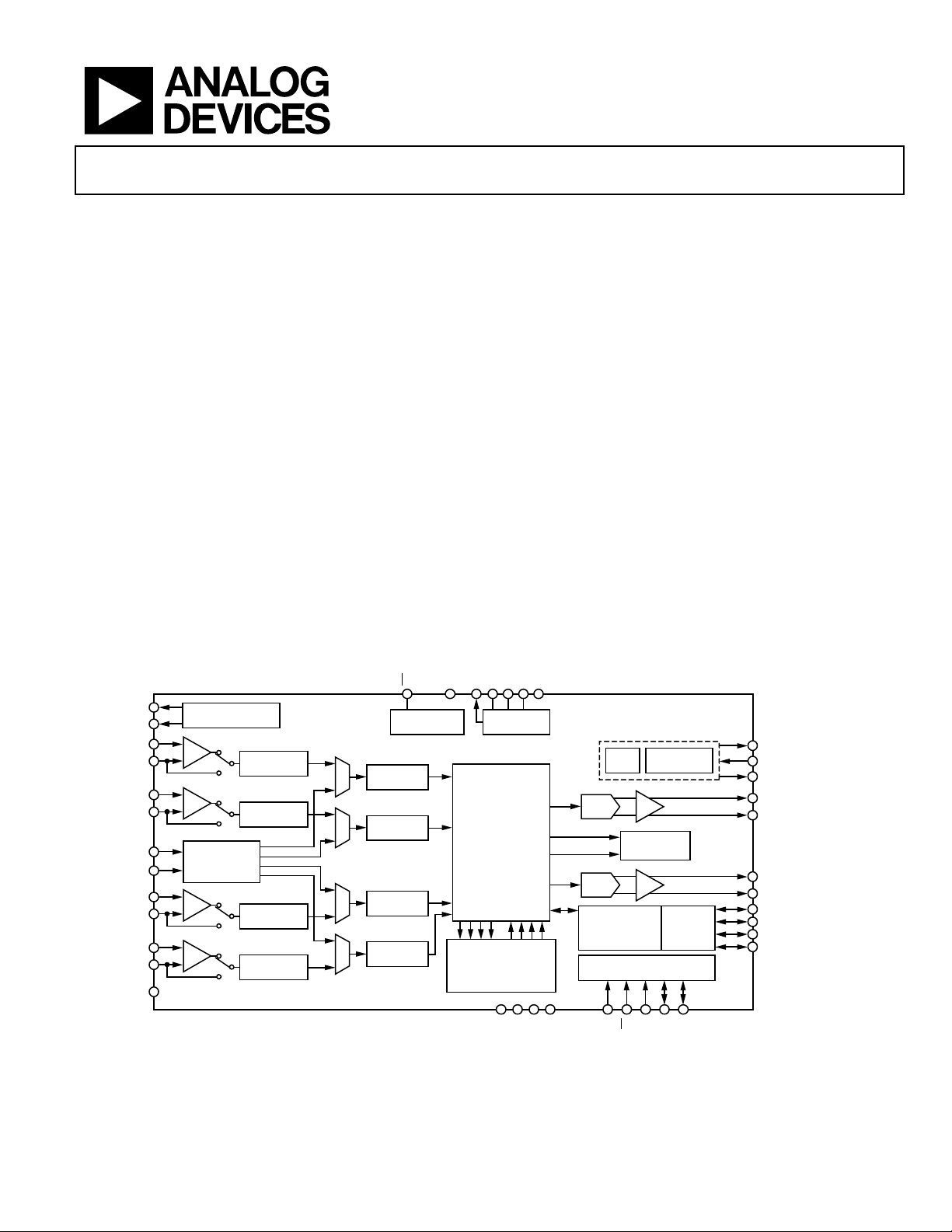
Four ADC, Two DAC Low Power Codec
with Audio Processor
ADAU1772
Rev. 0
third parties that may result from its use. Specifications subject to change without notice. No
Trademarks and registered trademarks are the prop erty of their respective owner s.
Fax: 781.461.3113 ©2012 Analog Devices, Inc. All rights reserved.
MICROPHONE
BIAS GENERATORS
MICBIAS0
MICBIAS1
CM
ADC
MODULATOR
ADC
DECIMATOR
AIN0REF
AIN0
PGA
ADC
MODULATOR
ADC
DECIMATOR
AIN1REF
AIN1
PGA
ADC
MODULATOR
AIN2REF
AIN2
PGA
ADC
MODULATOR
AIN3REF
AIN3
PGA
ADC
DECIMATOR
ADC
DECIMATOR
DMIC0_1/MP4
DMIC2_3/MP5
DIGITAL
MICROPHONE
INPUTS
INPUT/OUTPUT
SIGNAL
ROUTING
DSP CORE:
BIQUAD FILTERS,
LIMITERS,
VOLUME CONTROLS,
MIXING
I2C/SPI CONTROL
INTERFACE AND S E LF-BOOT
BIDIRECTIONAL
ASRCS
SERIAL
INPUT/
OUTPUT
PORT
LDO
REGULATOR
REG_OUT
AVDD
AVDD
AVDD
IOVDD
DVDD
POWER
MANAGEMENT
PD
PLL
CLOCK
OSCILLATOR
SELFBOOT
DGND
AGND
AGND
AGND
ADDR0/SS
ADDR1/MOSI
SCL/SCLK
SDA/MISO
DAC_SDATA/MP0
ADC_SDATA1/CLKOUT/MP6
XTALI/MCLKIN
XTALO
ADC_SDATA0/PDMOUT/MP1
BCLK/MP2
LRCLK/MP3
DAC
DAC
STEREO PDM
MODULATOR
ADAU1772
10804-001
HPOUTLP/LOUTLP
HPOUTLN/LOUTLN
HPOUTRP/LOUTRP
HPOUTRN/LOUTRN
Data Sheet
FEATURES
Programmable audio processing engine
192 kHz processing path
Biquad filters, limiters, volume controls, mixing
Low latency, 24-bit ADCs and DACs
102 dB SNR (signal through PGA and ADC
with A-weighted filter)
107 dB combined SNR (signal through DAC and headphone
with A-weighted filter)
Serial port sample rates from 8 kHz to 192 kHz
38 μs analog-to-analog latency
4 single-ended analog inputs—configurable as microphone
or line inputs
Dual stereo digital microphone inputs
Stereo analog audio output—single-ended or differential,
configurable as either line output or headphone driver
PLL supporting any input clock rate from 8 MHz to 27 MHz
Full-duplex, asynchronous sample rate converters (ASRCs)
Power supplies
Analog and digital I/O of 1.8 V to 3.3 V
Digital signal processing (DSP) core of 1.1 V to 1.8 V
FUNCTIONAL BLOCK DIAGRAM
Low power (15 mW for typical noise cancelling solution)
2
I
C and SPI control interfaces, self-boot from I2C EEPROM
7 MP pins supporting dual stereo digital microphone inputs,
stereo PDM output, mute, DSP bypass, push-button
volume controls, and parameter bank switching
APPLICATIONS
Noise cancelling handsets, headsets, and headphones
Bluetooth ANC handsets, headsets, and headphones
Personal navigation devices
Digital still and video cameras
GENERAL DESCRIPTION
The ADAU1772 is a codec with four inputs and two outputs that
incorporates a digital processing engine to perform filtering,
level control, signal level monitoring, and mixing. The path
from the analog input to the DSP core to the analog output is
optimized for low latency and is ideal for noise cancelling headsets.
With the addition of just a few passive components, a crystal,
and an EEPROM for booting, the ADAU1772 provides a
complete headset solution.
Information furnished by Analog Devices is believed to be accurate and reliable. However, no
responsibility is assumed by Analog Devices for its use, nor for any infringements of patents or other
rights of
license is granted by implication or otherwise under any patent or patent rights of Analog Devices.
Figure 1.
One Technology Way, P.O. Box 9106, Norwood, MA 02062-9106, U.S.A.
Tel: 781.329.4700 www.analog.com

ADAU1772 Data Sheet
TABLE OF CONTENTS
Features .............................................................................................. 1
Applications ....................................................................................... 1
General Description ......................................................................... 1
Functional Block Diagram .............................................................. 1
Revision History ............................................................................... 3
Specifications ..................................................................................... 4
Analog Performance Specifications ........................................... 4
Crystal Amplifier Specifications ................................................. 7
Digital Input/Output Specifications........................................... 8
Power Supply Specifications........................................................ 8
Typical Power Consumption ....................................................... 9
Digital Filters ................................................................................. 9
Digital Timing Specifications ................................................... 10
Absolute Maximum Ratings .......................................................... 14
Thermal Resistance .................................................................... 14
ESD Caution ................................................................................ 14
Pin Configuration and Function Descriptions ........................... 15
Typical Performance Characteristics ........................................... 17
System Block Diagrams ................................................................. 27
Theory of Operation ...................................................................... 28
System Clocking and Power-Up ................................................... 29
Clock Initialization ..................................................................... 29
PLL ............................................................................................... 29
Clock Output ............................................................................... 30
Power Sequencing ...................................................................... 30
Signal Routing ................................................................................. 31
Input Signal Paths ........................................................................... 32
Analog Inputs .............................................................................. 32
Digital Microphone Input ......................................................... 33
Analog-to-Digital Converters ................................................... 33
Output Signal Paths ........................................................................ 34
Analog Outputs........................................................................... 34
Digital-to-Analog Converters ................................................... 34
PDM Output ............................................................................... 34
Asynchronous Sample Rate Converters .................................. 35
Signal Levels ................................................................................ 35
Signal Processing ............................................................................ 36
Instructions ................................................................................. 36
Data Memory .............................................................................. 36
Parameters ................................................................................... 36
Control Port .................................................................................... 39
I2C Port ........................................................................................ 39
SPI Port ........................................................................................ 42
Self-Boot ...................................................................................... 43
Multipurpose Pins .......................................................................... 44
Push-Button Volume Controls ................................................. 44
Limiter Compression Enable .................................................... 44
Parameter Bank Switching ........................................................ 44
Mute ............................................................................................. 44
DSP Bypass Mode ...................................................................... 45
Serial Data Input/Output Ports .................................................... 46
Tristating Unused Channels...................................................... 46
Applications Information .............................................................. 49
Power Supply Bypass Capacitors .............................................. 49
Layout .......................................................................................... 49
Grounding ................................................................................... 49
Exposed Pad PCB Design ......................................................... 49
Register Summary .......................................................................... 50
Register Details ............................................................................... 52
Clock Control Register .............................................................. 52
PLL Denominator MSB Register .............................................. 53
PLL Denominator LSB Register ............................................... 53
PLL Numerator MSB Register .................................................. 53
PLL Numerator LSB Register .................................................... 54
PLL Integer Setting Register ..................................................... 54
PLL Lock Flag Register .............................................................. 55
CLKOUT Setting Selection Register ........................................ 55
Regulator Control Register ....................................................... 56
Core Control Register ................................................................ 57
Filter Engine and Limiter Control Register ............................ 58
DB Value Register 0 Read .......................................................... 59
DB Value Register 1 Read .......................................................... 59
DB Value Register 2 Read .......................................................... 60
Core Channel 0/Core Channel 1 Input Select Register ......... 61
Core Channel 2/Core Channel 3 Input Select Register ......... 62
DAC Input Select Register ........................................................ 63
PDM Modulator Input Select Register .................................... 64
Serial Data Output 0/Serial Data Output 1 Input Select
Register ........................................................................................ 65
Rev. 0 | Page 2 of 116

Data Sheet ADAU1772
Serial Data Output 2/Serial Data Output 3 Input Select
Register ......................................................................................... 66
Serial Data Output 4/Serial Data Output 5 Input Select
Register ......................................................................................... 67
Serial Data Output 6/Serial Data Output 7 Input Select
Register ......................................................................................... 68
ADC_SDATA0/ADC_SDATA1 Channel Select Register ...... 69
Output ASRC0/Output ASRC1 Source Register ..................... 70
Output ASRC2/Output ASRC3 Source Register ..................... 71
Input ASRC Channel Select Register ........................................ 72
ADC0/ADC1 Control 0 Register .............................................. 73
ADC2/ADC3 Control 0 Register .............................................. 74
ADC0/ADC1 Control 1 Register .............................................. 75
ADC2/ADC3 Control 1 Register .............................................. 76
ADC0 Volume Control Register ............................................... 77
ADC1 Volume Control Register ............................................... 77
ADC2 Volume Control Register ............................................... 78
ADC3 Volume Control Register ............................................... 78
PGA Control 0 Register .............................................................. 79
PGA Control 1 Register .............................................................. 79
PGA Control 2 Register .............................................................. 80
PGA Control 3 Register .............................................................. 81
PGA Slew Control Register ........................................................ 82
PGA 10 dB Gain Boost Register ................................................ 83
Input and Output Capacitor Charging Register ..................... 84
DSP Bypass Path Register .......................................................... 85
DSP Bypass Gain for PGA0 Register ........................................ 85
DSP Bypass Gain for PGA1 Register ........................................ 85
MIC_BIAS0_1 Control Register ............................................... 86
DAC Control Register ................................................................ 86
DAC0 Volume Control Register ................................................ 87
DAC1 Volume Control Register ................................................ 87
Headphone Output Mutes Register .......................................... 88
Serial Port Control 0 Register .................................................... 89
Serial Port Control 1 Register .................................................... 90
TDM Output Channel Disable Register .................................. 91
PDM Enable Register ................................................................. 92
PDM Pattern Setting Register ................................................... 93
MP0 Function Setting Register ................................................. 93
MP1 Function Setting Register ................................................. 94
MP2 Function Setting Register ................................................. 95
MP3 Function Setting Register ................................................. 96
MP4 Function Setting Register ................................................. 97
MP5 Function Setting Register ................................................. 98
MP6 Function Setting Register ................................................. 99
Push-Button Volume Settings Register .................................. 100
Push-Button Volume Control Assignment Register ............ 101
Debounce Modes Register ....................................................... 102
Headphone Line Output Select Register ................................ 102
Decimator Power Control Register ........................................ 104
ASRC Interpolator and DAC Modulator Power Control
Register ....................................................................................... 105
Analog Bias Control 0 Register ............................................... 105
Analog Bias Control 1 Register ............................................... 106
Digital Pin Pull-Up Control 0 Register .................................. 107
Digital Pin Pull-Up Control 1 Register .................................. 108
Digital Pin Pull-Down Control 0 Register ............................ 109
Digital Pin Pull-Down Control 1 Register ............................ 110
Digital Pin Drive Strength Control 0 Register ...................... 111
Digital Pin Drive Strength Control 1 Register ...................... 112
Outline Dimensions ...................................................................... 113
Ordering Guide ......................................................................... 113
REVISION HISTORY
7/12—Revision 0: Initial Version
Rev. 0 | Page 3 of 116

ADAU1772 Data Sheet
Parameter
Test Conditions/Comments
Min
Typ
Max
Unit
Single-Ended Line Input
0 dB gain
14.3 kΩ
AVDD = 1.8 V
−90 dB
AVDD = 1.8 V
0.49 V rms
SPECIFICATIONS
Master clock = core clock = 12.288 MHz, serial input sample rate = 48 kHz, measurement bandwidth = 20 Hz to 20 kHz, word width =
24 bits, ambient temperature = 25°C, outputs line loaded with 10 kΩ.
ANALOG PERFORMANCE SPECIFICATIONS
Supply voltages AVDD = IOVDD = 1.8 V, DVDD = 1.1 V, unless otherwise noted. PLL disabled, direct master clock.
Table 1.
ANALOG-TO-DIGITAL CONVERTERS
ADC Resolution All ADCs 24 Bits
Digital Attenuation Step 0.375 dB
Digital Attenuation Range 95 dB
INPUT RESISTANCE Gain settings do not include 10 dB gain from
PGA Inputs −12 dB gain 32.0 kΩ
0 dB gain 20 kΩ
+35.25 dB gain 0.68 kΩ
SINGLE-ENDED LINE INPUT PGA_ENx = 0, PGA_x_BOOST = 0, PGA_POP_DISx = 1
Full-Scale Input Voltage Scales linearly with AVDD AVDD/3.63 V rms
AVDD = 1.8 V 0.49 V rms
AVDD = 1.8 V, 0 dBFS 1.38 V p-p
AVDD = 3.3 V 0.90 V rms
AVDD = 3.3 V, 0 dBFS 2.54 V p-p
Dynamic Range
With A-Weighted Filter (RMS) AVDD = 1.8 V 97 dB
AVDD = 3.3 V 102 dB
With Flat 20 Hz to 20 kHz Filter AVDD = 1.8 V 94 dB
AVDD = 3.3 V 99 dB
Signal-to-Noise Ratio (SNR)
With A-Weighted Filter (RMS) AVDD = 1.8 V 98 dB
AVDD = 3.3 V 103 dB
With Flat 20 Hz to 20 kHz Filter AVDD = 1.8 V 96 dB
AVDD = 3.3 V 100 dB
Interchannel Gain Mismatch 40 mdB
Total Harmonic Distortion + Noise (THD + N) 20 Hz to 20 kHz, −1 dBFS
1
2
PGA_x_BOOST settings; this additional gain does
not affect input impedance; PGA_POP_DISx = 1
20 Hz to 20 kHz, −60 dB input
AVDD = 3.3 V −94 dB
Offset Error ±0.1 mV
Gain Error ±0.2 dB
Interchannel Isolation CM capacitor = 22 μF 100 dB
Power Supply Rejection Ratio CM capacitor = 22 μF
100 mV p-p at 1 kHz 55 dB
SINGLE-ENDED PGA INPUT PGA_ENx = 1, PGA_x_BOOST = 0
Full-Scale Input Voltage Scales linearly with AVDD AVDD/3.63 V rms
AVDD = 1.8 V, 0 dBFS 1.38 V p-p
AVDD = 3.3 V 0.90 V rms
AVDD = 3.3 V, 0 dBFS 2.54 V p-p
Dynamic Range
With A-Weighted Filter (RMS) AVDD = 1.8 V 96 dB
AVDD = 3.3 V 102 dB
With Flat 20 Hz to 20 kHz Filter AVDD = 1.8 V 94 dB
AVDD = 3.3 V 99 dB
1
20 Hz to 20 kHz, −60 dB input
Rev. 0 | Page 4 of 116

Data Sheet ADAU1772
Interchannel Isolation
83 dB
Output Impedance
1 Ω
Parameter Test Conditions/Comments Min Typ Max Unit
Total Harmonic Distortion + Noise 20 Hz to 20 kHz, −1 dBFS
AVDD = 1.8 V −88 dB
AVDD = 3.3 V −90 dB
Signal-to-Noise Ratio
With A-Weighted Filter (RMS) AVDD = 1.8 V 96 dB
AVDD = 3.3 V 102 dB
With Flat 20 Hz to 20 kHz Filter AVDD = 1.8 V 94 dB
AVDD = 3.3 V 99 dB
PGA Gain Variation
With −12 dB Setting Standard deviation 0.05 dB
With +35.25 dB Setting Standard deviation 0.15 dB
PGA Boost PGA_x_BOOST 10 dB
PGA Mute Attenuation PGA_MUTEx −65 dB
Interchannel Gain Mismatch 0.005 dB
Offset Error 0 mV
Gain Error ±0.2 dB
Power Supply Rejection Ratio CM capacitor = 22 μF, 100 mV p-p at 1 kHz 63 dB
MICROPHONE BIAS MIC_ENx = 1
Bias Voltage
0.65 × AVDD AVDD = 1.8 V, MIC_GAINx = 1 1.16 V
AVDD = 3.3 V, MIC_GAINx = 1 2.12 V
0.90 × AVDD AVDD = 1.8 V, MIC_GAINx = 0 1.63 V
AVDD = 3.3 V, MIC_GAINx = 0 2.97 V
Bias Current Source 3 mA
2
MICBIASx Isolation MIC_GAINx = 0 95 dB
MIC_GAINx = 1 99 dB
Noise in the Signal Bandwidth3 AVDD = 1.8 V, 20 Hz to 20 kHz
MIC_GAINx = 0 27 nV/√Hz
MIC_GAINx = 1 16 nV/√Hz
AVDD = 3.3 V, 20 Hz to 20 kHz
MIC_GAINx = 0 35 nV/√Hz
MIC_GAINx = 1 19 nV/√Hz
DIGITAL-TO-ANALOG CONVERTERS
DAC Resolution All DACs 24 Bits
Digital Attenuation Step 0.375 dB
Digital Attenuation Range 95 dB
DAC SINGLE-ENDED OUTPUT Single-ended operation, HPOUTLP and
HPOUTRP pins
Full-Scale Output Voltage Scales linearly with AVDD AVDD/3.4 V rms
AVDD = 1.8 V 0.53 V rms
AVDD = 1.8 V, 0 dBFS 1.5 V p-p
AVDD = 3.3 V 0.97 V rms
AVDD = 3.3 V, 0 dBFS 2.74 V p-p
Mute Attenuation −72 dB
Dynamic Range
1
Line output mode, 20 Hz to 20 kHz, −60 dB input
With A-Weighted Filter (RMS) AVDD = 1.8 V 100 dB
AVDD = 3.3 V 104 dB
With Flat 20 Hz to 20 kHz Filter AVDD = 1.8 V 97 dB
AVDD = 3.3 V 101 dB
Signal-to-Noise Ratio
2
Line output mode, 20 Hz to 20 kHz
With A-Weighted Filter (RMS) AVDD = 1.8 V 100 dB
AVDD = 3.3 V 104 dB
With Flat 20 Hz to 20 kHz Filter AVDD = 1.8 V 98 dB
AVDD = 3.3 V 102 dB
Rev. 0 | Page 5 of 116

ADAU1772 Data Sheet
AVDD = 3.3 V, <0.1% THD + N
28.1 mW
With A-Weighted Filter (RMS)
AVDD = 1.8 V
105 dB
Parameter Test Conditions/Comments Min Typ Max Unit
Interchannel Gain Mismatch Line output mode 20 mdB
Total Harmonic Distortion + Noise Line output mode, 20 Hz to 20 kHz, −1 dBFS dB
AVDD = 1.8 V −93 dB
AVDD = 3.3 V −94 dB
Gain Error Line output mode ±0.1 dB
Dynamic Range
With A-Weighted Filter (RMS) AVDD = 1.8 V 100 dB
AVDD = 3.3 V 104 dB
With Flat 20 Hz to 20 kHz Filter AVDD = 1.8 V 97 dB
AVDD = 3.3 V 101 dB
Signal-to-Noise Ratio
With A-Weighted Filter (RMS) AVDD = 1.8 V 100 dB
AVDD = 3.3 V 104 dB
With Flat 20 Hz to 20 kHz Filter AVDD = 1.8 V 98 dB
AVDD = 3.3 V 102 dB
Interchannel Gain Mismatch Headphone mode 50 mdB
Total Harmonic Distortion + Noise Headphone mode, 20 Hz to 20 kHz, −1 dBFS
32 Ω load AVDD = 1.8 V, PO = 6.7 mW −77 dB
AVDD = 3.3 V, PO = 22.4 mW −80 dB
24 Ω load AVDD = 1.8 V, PO = 8.9 mW −76 dB
AVDD = 3.3 V, PO = 30 mW −79 dB
16 Ω load AVDD = 1.8 V, PO = 13 mW −74 dB
AVDD = 3.3 V, PO = 44 mW −77 dB
Headphone Output Power
32 Ω Load AVDD = 1.8 V, <0.1% THD + N 8.4 mW
1
2
Headphone mode, 20 Hz to 20 kHz, −60 dB input
Headphone mode, 20 Hz to 20 kHz
24 Ω Load AVDD = 1.8 V, <0.1% THD + N 11.2 mW
AVDD = 3.3 V, <0.1% THD + N 37.4 mW
16 Ω Load AVDD = 1.8 V, <0.1% THD + N 16.25 mW
AVDD = 3.3 V, <0.1% THD + N 55.8 mW
Gain Error Headphone mode ±0.1 dB
Offset Error ±0.1 mV
Interchannel Isolation 1 kHz, 0 dBFS input signal 100 dB
Power Supply Rejection Ratio CM capacitor = 22 μF, 100 mV p-p at 1 kHz 70 dB
DAC DIFFERENTIAL OUTPUT Differential operation
Full-Scale Output Voltage Scales linearly with AVDD AVDD/1.8 V rms
AVDD = 1.8 V 1.0 V rms
AVDD = 1.8 V, 0 dBFS 2.58 V p-p
AVDD = 3.3 V 1.83 V rms
AVDD = 3.3 V, 0 dBFS 5.49 V p-p
Mute Attenuation −72 dB
Dynamic Range
1
Line output mode, 20 Hz to 20 kHz, −60 dB input
With A-Weighted Filter (RMS) AVDD = 1.8 V 104 dB
AVDD = 3.3 V 107 dB
With Flat 20 Hz to 20 kHz Filter AVDD = 1.8 V 101 dB
AVDD = 3.3 V 105 dB
Signal-to-Noise Ratio
2
Line output mode, 20 Hz to 20 kHz
AVDD = 3.3 V 108 dB
With Flat 20 Hz to 20 kHz Filter AVDD = 1.8 V 102 dB
AVDD = 3.3 V 105 dB
Interchannel Gain Mismatch Line output mode 20 mdB
Total Harmonic Distortion + Noise Line output mode, 20 Hz to 20 kHz, −1 dBFS dB
AVDD = 1.8 V −96 dB
AVDD = 3.3 V −96 dB
Gain Error Line output mode %
Rev. 0 | Page 6 of 116

Data Sheet ADAU1772
16 Ω Load
−3 dBFS, AVDD = 1.8 V, PO = 33 mW
−75 dB
Parameter
Jitter
270
500
ps
Parameter Test Conditions/Comments Min Typ Max Unit
Dynamic Range
With A-Weighted Filter (RMS) AVDD = 1.8 V 104 dB
AVDD = 3.3 V 107 dB
With Flat 20 Hz to 20 kHz Filter AVDD = 1.8 V 102 dB
AVDD = 3.3 V 104 dB
Signal-to-Noise Ratio
With A-Weighted Filter (RMS) AVDD = 1.8 V 105 dB
AVDD = 3.3 V 108 dB
With Flat 20 Hz to 20 kHz Filter AVDD = 1.8 V 103 dB
AVDD = 3.3 V 106 dB
Interchannel Gain Mismatch Headphone mode 75 mdB
Total Harmonic Distortion + Noise Headphone mode
32 Ω Load −1 dBFS, AVDD = 1.8 V, PO = 27 mW −75 dB
−1 dBFS, AVDD = 3.3 V, PO = 90 mW −83 dB
24 Ω Load −2 dBFS, AVDD = 1.8 V, PO = 28 mW −75 dB
−1 dBFS, AVDD = 3.3 V, PO = 118 mW −77 dB
−1 dBFS, AVDD = 3.3 V, PO = 175 mW −83 dB
Headphone Output Power
32 Ω Load AVDD = 1.8 V, <0.1% THD + N 32.5 mW
AVDD = 3.3 V, <0.1% THD + N 111.8 mW
24 Ω Load AVDD = 1.8 V, <0.1% THD + N 37.6 mW
AVDD = 3.3 V, <0.1% THD + N 148.3 mW
16 Ω Load AVDD = 1.8 V, <0.1% THD + N 41.5 mW
AVDD = 3.3 V, <0.1% THD + N 189.2 mW
Gain Error Headphone mode ±0.25 %
Offset Error ±0.1 mV
Interchannel Isolation 1 kHz, 0 dBFS input signal 100 dB
Power Supply Rejection Ratio CM capacitor = 22 μF
100 mV p-p at 1 kHz 73 dB
CM REFERENCE CM pin
Common-Mode Reference Output AVDD/2 V
Common-Mode Source Impedance 5 kΩ
REGULATOR
Line Regulation 1 mV/V
Load Regulation 6 mV/mA
1
Dynamic range is the ratio of the sum of noise and harmonic power in the band of interest with a −60 dBFS signal present to the full-scale power level in decibels.
2
SNR is the ratio of the sum of all noise power in the band of interest with no signal present to the full-scale power level in decibels.
3
These specifications are with 4.7 µF decoupling and 5.0 kΩ load on pin.
CRYSTAL AMPLIFIER SPECIFICATIONS
Supply voltages AVDD = IOVDD = 1.8 V, DVDD = 1.1 V, unless otherwise noted.
1
2
Headphone mode, 20 Hz to 20 kHz, −60 dB input
Headphone mode, 20 Hz to 20 kHz
Table 2.
Frequency Range 8 27 MHz
Load Capacitance 20 pF
Test Conditions/Comments Min Typ Max Unit
Rev. 0 | Page 7 of 116

ADAU1772 Data Sheet
IIL at VIL = 0.8 V
10
µA
Digital I/O Current with IOVDD = 1.8 V
Crystal oscillator enabled
fS = 8 kHz
0.35 mA
fS = 8 kHz
1.99 mA
DIGITAL INPUT/OUTPUT SPECIFICATIONS
−40°C < TA < +85°C, IOVDD = 3.3 V ± 10% and 1.8 V − 5%/+10%.
Table 3.
Parameter Test Conditions/Comments Min Typ Max Unit
Input Voltage High (VIH) IOVDD = 3.3 V 2.0 V
IOVDD = 1.8 V 1.1 V
Input Voltage Low (VIL) IOVDD = 3.3 V 0.8 V
IOVDD = 1.8 V 0.45 V
Input Leakage IOVDD = 3.3 V, IIH at VIH = 2.0 V 10 µA
IOVDD = 1.8 V, IIH at VIH = 1.1 V 10 µA
IIL at VIL = 0.45 V 10 µA
Output Voltage High (VOH) with Low Drive Strength IOH = 1 mA IOVDD − 0.6 V
Output Voltage High (VOH) with High Drive Strength IOH = 3 mA IOVDD − 0.6 V
Output Voltage Low (VOL) with Low Drive Strength IOL = 1 mA 0.4 V
Output Voltage Low (VOL) with High Drive Strength IOL = 3 mA 0.4 V
Input Capacitance 5 pF
POWER SUPPLY SPECIFICATIONS
Supply voltages AVDD = IOVDD = 1.8 V, DVDD = 1.1 V, unless otherwise noted. PLL disabled, direct master clock.
Table 4.
Parameter Test Conditions/Comments Min Typ Max Unit
SUPPLIES
AVDD Voltage 1.71 1.8 3.63 V
DVDD Voltage 1.045 1.1 1.98 V
IOVDD Voltage 1.71 1.8 3.63 V
Slave Mode fS = 48 kHz 0.35 mA
fS = 192 kHz 0.49 mA
fS = 8 kHz 0.32 mA
Master Mode fS = 48 kHz 0.53 mA
fS = 192 kHz 1.18 mA
Power-Down 0 µA
Digital I/O Current with IOVDD = 3.3 V Crystal oscillator enabled
Slave Mode fS = 48 kHz 2.05 mA
fS = 192 kHz 2.28 mA
Master Mode fS = 48 kHz 2.4 mA
fS = 192 kHz 3.62 mA
fS = 8 kHz 2.05 mA
Power-Down 7 µA
Analog Current (AVDD) See Table 5
Power-Down AVDD = 1.8 V 0.6 µA
AVDD = 3.3 V 13.6 µA
DISSIPATION
Operation fS = 192 kHz (see conditions in Table 5)
All Supplies 15.5 mW
Digital I/O Supply 0.7 mW
Analog Supply Includes regulated DVDD current 14.8 mW
Power-Down, All Supplies 1 µW
Rev. 0 | Page 8 of 116

Data Sheet ADAU1772
Enhanced performance
12.65
−93
−90.5
Power saving
7.78
−84.5
−87.5
Dynamic Range
100 dB
PDM MODULATOR
TYPICAL POWER CONSUMPTION
Typical active noise cancelling (ANC) settings. Master clock = 12.288 MHz, fS = 192 kHz. On-board regulator enabled. Two analog-todigital converters (ADCs) with PGA enabled and two ADCs configured for line input; no input signal. Two digital-to-analog converters
(DACs) configured for differential headphone operation; DAC outputs unloaded. Both MICBIAS0 and MICBIAS1 enabled. ASRCs and
pulse density modulated (PDM) modulator disabled. Core running 26 out of 32 possible instructions. For total power consumption, add
IOVDD at 8 kHz slave current listed in Tabl e 4.
Table 5.
Typical AVDD Power Consumption
Operating Voltage Power Management Setting
AVDD = IOVDD = 3.3 V Normal (default) 11.5 −93 −87.5
Extreme power saving 9.4 −93 −86.5
Power saving 9.8 −93 −86.5
AVDD = IOVDD = 1.8 V Normal (default) 9.37 −86 −91
Extreme power saving 7.40 −84.5 −87
Enhanced performance 10.4 −86 −94.5
(mA)
DIGITAL FILTERS
Table 6.
Parameter Test Conditions/Comments Min Typ Max Unit
ADC INPUT TO DAC OUTPUT PATH
Pass-Band Ripple DC to 20 kHz, fS = 192 kHz ±0.02 dB
Group Delay fS = 192 kHz 38 µs
SAMPLE RATE CONVERTER
Pass Band LRCLK < 63 kHz 0 0.475 × fS kHz
63 kHz < LRCLK <130 kHz 0 0.4286 × fS
LRCLK > 130 kHz 0 0.4286 × fS
Pass-Band Ripple Upsampling, 96 kHz −0.27 0.05 dB
Upsampling, 192 kHz −0.06 0.05 dB
Downsampling, 96 kHz 0 0.07 dB
Downsampling, 192 kHz 0 0.07 dB
Input/Output Frequency Range 8 192 kHz
Typical ADC THD + N
(dB)
Typical HP Output
THD + N (dB)
Total Harmonic Distortion + Noise −90 dB
Startup Time 15 ms
Dynamic Range (A-Weighted) 112 dB
Total Harmonic Distortion + Noise −92 dB
Rev. 0 | Page 9 of 116

ADAU1772 Data Sheet
tLS
10 ns
LRCLK setup; time to BCLK rising (slave mode)
t
30
ns
BCLK falling to ADC_SDATAx driven in TDM tristate mode
t
80 ns
SS pulse width high
t
250
ns
SDA fall time; C
= 400 pF
t
6 × tMP – 70
ns
Delay from SCL falling to SDA changing
MULTIPURPOSE AND POWER-
DIGITAL TIMING SPECIFICATIONS
−40°C < TA < +85°C, IOVDD = 1.71 V to 3.63 V, DVDD = 1.045 V to 1.98 V.
Table 7. Digital Timing
Limit
Parameter T
MASTER CLOCK
tMP 37 125 ns MCLKIN period; 8 MHz to 27 MHz input clock using PLL
t
77 82 ns Internal MCLK period; direct MCLK and PLL output divided by 2
MCLK
SERIAL PORT
tBL 40 ns BCLK low pulse width (master and slave modes)
tBH 40 ns BCLK high pulse width (master and slave modes)
tLH 10 ns LRCLK hold; time from BCLK rising (slave mode)
tSS 5 ns DAC_SDATA setup; time to BCLK rising (master and slave modes)
tSH 5 ns DAC_SDATA hold; time from BCLK rising (master and slave modes)
tTS 10 ns BCLK falling to LRCLK timing skew (master mode)
t
0 34 ns ADC_SDATAx delay; time from BCLK falling (master and slave modes)
SOD
SOTD
t
30 ns BCLK falling to ADC_SDATAx tristated in TDM tristate mode
SOTX
SPI PORT
f
SCLK
t
80 ns SCLK pulse width low
CCPL
t
80 ns SCLK pulse width high
CCPH
t
5 ns SS setup; time to SCLK rising
CLS
t
100 ns SS hold; time from SCLK rising
CLH
CLPH
t
10 ns MOSI setup; time to SCLK rising
CDS
t
10 ns MOSI hold; time from SCLK rising
CDH
t
101 ns MISO delay; time from SCLK falling
COD
I2C PORT
f
SCL
t
0.6 µs SCL high
SCLH
t
1.3 µs SCL low
SCLL
t
0.6 µs
SCS
t
250 ns SCL and SDA rise time, C
SCR
t
0.6 µs SCL fall hold time (from SDA falling), relevant for start condition
SCH
tDS 100 ns SDA setup time (to SCL rising)
t
250 ns SCL fall time; C
SCF
SDF
t
0.6 µs SCL rise setup time (to SDA rising), relevant for stop condition
BFT
I2C EEPROM SELF-BOOT
t
26 × tMP – 70 ns
SCHE
t
38 × tMP – 70 ns
SCSE
t
70 × tMP – 70 ns SCL rise setup time (to SDA rising), relevant for stop condition
BFTE
DSE
t
32 × tMP ns
BHTE
T
MIN
Unit Description
MAX
6.25 MHz SCLK frequency
400 kHz SCL frequency
SCL rise setup time (to SDA falling), relevant for repeated start
condition
SCL fall hold time (from SDA falling), relevant for start condition; t
is the input clock on the MCLKIN pin
SCL rise setup time (to SDA falling), relevant for repeated start
condition
SDA rising in self-boot stop condition to SDA falling edge for
external master start condition
= 400 pF
LOAD
LOAD
= 400 pF
LOAD
MP
DOWN PINS
t
1.5 × 1/f
GIL
t
20 ns
RLPW
µs MPx input latency; time until high or low value is read by core
S
PD low pulse width
Rev. 0 | Page 10 of 116
Data Sheet ADAU1772
DIGITAL MICROPHONE
t
0
30
ns
PDM delay time for valid data
BCLK
LRCLK
DAC_SDATA
LEFT-JUSTIFIED
MODE
LSB
DAC_SDATA
I
2
S MODE
DAC_SDATA
RIGHT-JUSTIFIED
MODE
t
BH
MSB
MSB – 1
MSB
MSB
8-BIT CLOCKS
(24-BIT DAT A)
12-BIT CLOCKS
(20-BIT DAT A)
14-BIT CLOCKS
(18-BIT DAT A)
16-BIT CLOCKS
(16-BIT DAT A)
t
LS
t
SS
t
SH
t
SH
t
SS
t
SS
t
SH
t
SS
t
SH
t
LH
t
BL
10804-002
Limit
Parameter T
tCF 20 ns Digital microphone clock fall time
tCR 20 ns Digital microphone clock rise time
tDS 40 Digital microphone valid data start time
tDE 0 ns Digital microphone valid data end time
PDM OUTPUT
t
20 ns PDM clock fall time
DCF
t
20 ns PDM clock rise time
DCR
DDV
Digital Timing Diagrams
T
MIN
Unit Description
MAX
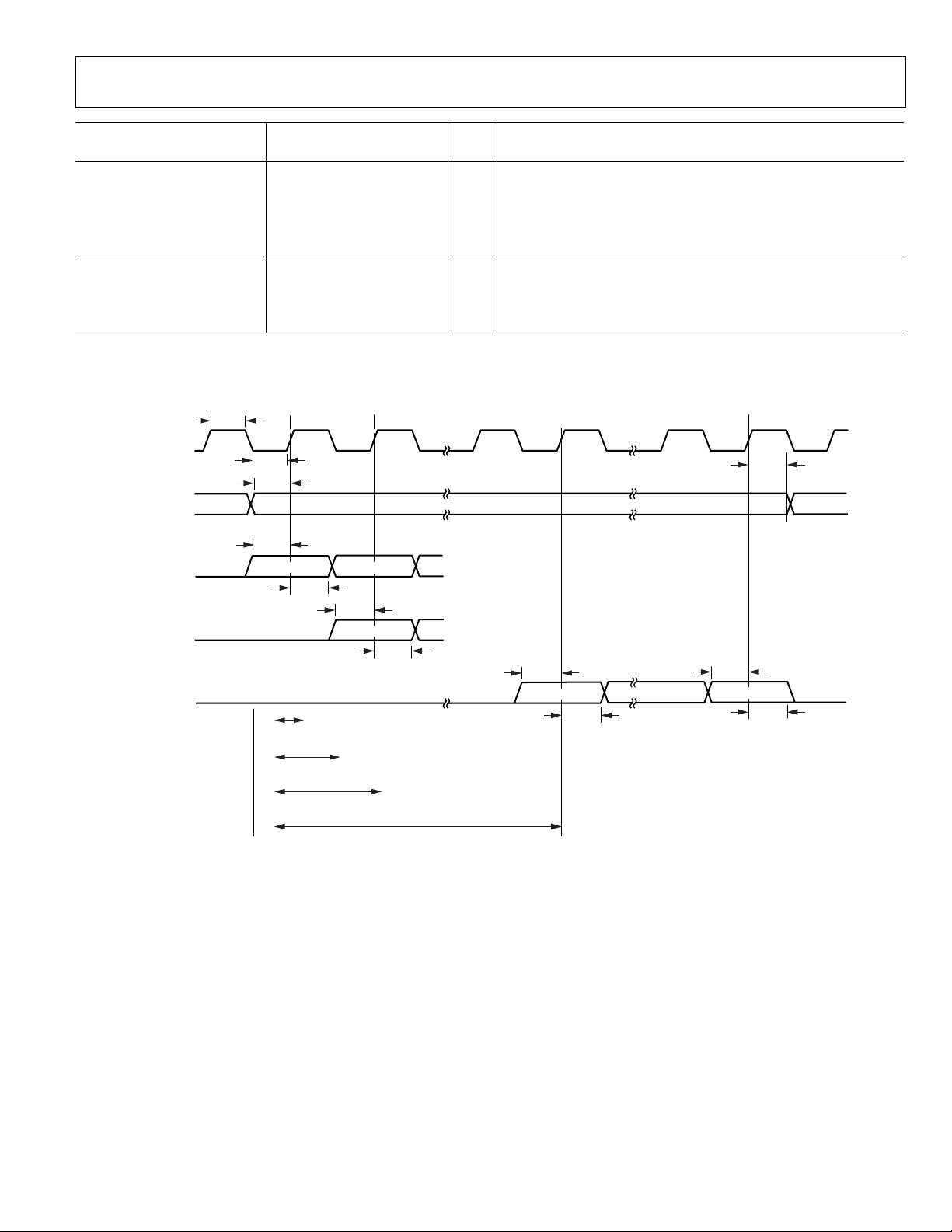
Figure 2. Serial Input Port Timing
Rev. 0 | Page 11 of 116
ADAU1772 Data Sheet
LRCLK
LSB
ADC_SDATAx
I
2
S MODE
ADC_SDATAx
RIGHT-JUSTIFIED
MODE
MSB
ADC_SDATAx
LEFT-JUSTIFIED
MODE
MSB
MSB – 1
ADC_SDATAx
W/TRISTATE MSB
LSB
MSB
8-BIT CLOCKS
(24-BIT DAT A)
12-BIT CLOCKS
(20-BIT DAT A)
14-BIT CLOCKS
(18-BIT DAT A)
16-BIT CLOCKS
(16-BIT DAT A)
t
LS
t
SOD
t
SOD
t
SOTD
t
SOD
t
SOTX
t
LH
t
TS
t
BL
BCLK
t
BH
HIGH-Z HIGH-Z
10804-003
SS
SCLK
MOSI
MISO
t
CLS
t
CDS
t
CDH
t
COD
t
CCPH
t
CCPL
t
CLH
t
CLPH
10804-004
t
SCH
t
SCLH
t
SCR
t
SCLL
t
SCF
t
DS
SDA
SCL
t
SCH
t
BFT
t
SCS
10804-005
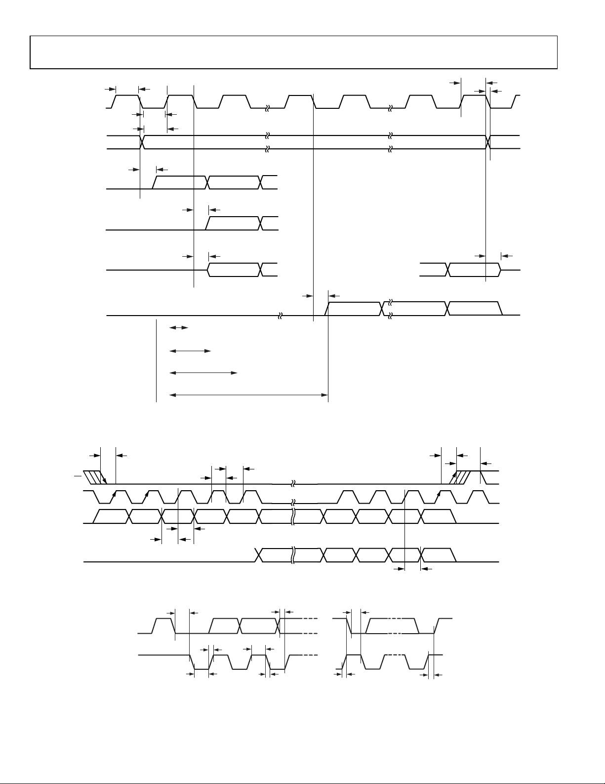
Figure 3. Serial Output Port Timing
Figure 4. SPI Port Timing
Figure 5. I
2
C Port Timing
Rev. 0 | Page 12 of 116
Data Sheet ADAU1772
t
SCHE
t
DSE
t
SCSE
t
BFTE
t
BHTE
SDA
SCL
10804-006
DMIC0_1/DMIC2_3
VALID LEFT SAMPLE VALID LEFT SAMPLEVALID RIGHT SAMPLE
CLKOUT
t
CR
t
CF
t
DS
t
DE
t
DS
t
DE
10804-007
t
DCF
PDMOUT
CLKOUT
RIGHT LEFT RIGHT LEFT
t
DCR
t
DDV
t
DDV
10804-008
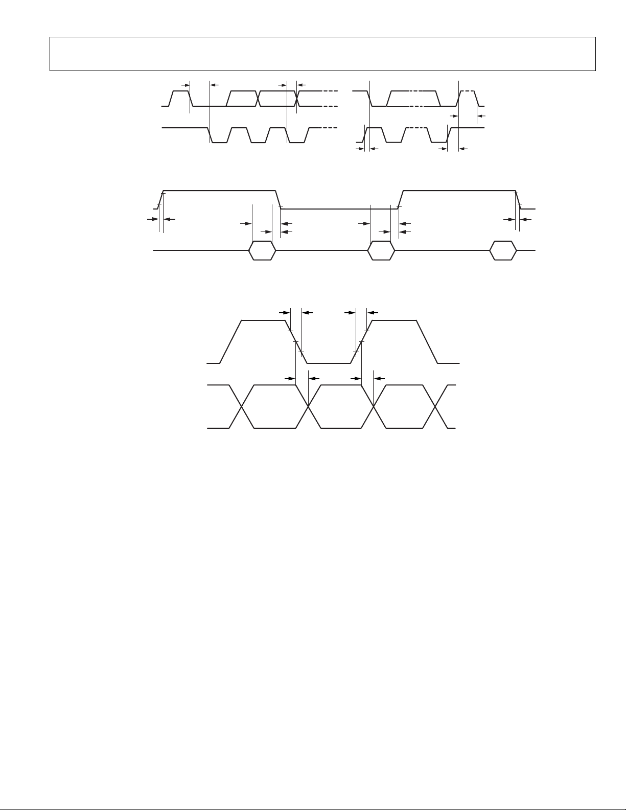
Figure 6. I
2
C Self-Boot Timing
Figure 7. Digital Microphone Timing
Figure 8. PDM Output Timing
Rev. 0 | Page 13 of 116
ADAU1772 Data Sheet
Digital Supply (DVDD)
−0.3 V to +1.98 V
40-Lead LFCSP
29
1.8
°C/W
ABSOLUTE MAXIMUM RATINGS
Table 8.
Parameter Rating
Power Supply (AVDD, IOVDD) −0.3 V to +3.63 V
Input Current (Except Supply Pins) ±20 mA
Analog Input Voltage (Signal Pins) –0.3 V to AVDD + 0.3 V
Digital Input Voltage (Signal Pins) −0.3 to IOVDD + 0.3 V
Operating Temperature Range (Case) −40°C to +85°C
Storage Temperature Range −65°C to +150°C
Stresses above those listed under Absolute Maximum Ratings
may cause permanent damage to the device. This is a stress
rating only; functional operation of the device at these or any
other conditions above those indicated in the operational
section of this specification is not implied. Exposure to absolute
maximum rating conditions for extended periods may affect
device reliability.
THERMAL RESISTANCE
θ
represents the junction-to-ambient thermal resistance; θ
JA
represents the junction-to-case thermal resistance. Thermal
numbers are simulated on a 4-layer JEDEC PCB with the
exposed pad soldered to the PCB. θ
was simulated at the
JC
exposed pad on the bottom of the package.
Table 9. Thermal Resistance
Package Type θ
JA
θ
JC
Unit
ESD CAUTION
JC
Rev. 0 | Page 14 of 116

Data Sheet ADAU1772
1SDA/MISO
2SCL/SCLK
3ADDR1/MOSI
4ADDR0/SS
5SELFBOOT
6MICBIAS0
7MICBIAS1
8AIN0REF
9AIN0
10AVDD
23 AGND
24 AVDD
25 HPOUTRN/LOUTRN
26 HPOUTRP/LOUTRP
27 PD
28 REG_OUT
29 DVDD
30 DGND
22 HPOUTLP/LOUTLP
21 HPOUTLN/LOUTLN
11AGND
12CM
13AIN1REF
15AIN2REF
17AIN3REF
16AIN2
18
AIN3
19AVDD
20AGND
14AIN1
33
DAC_SDATA/MP0
34
ADC_SDATA0/PDMOUT/MP1
35
ADC_SDATA1/CLKOUT/MP6
36
DMIC2_3/MP5
37
DMIC0_1/MP4
38
XTALO
39
XTALI/MCLKIN
40
IOVDD
32
BCLK/MP2
31
LRCLK/MP3
TOP VIEW
(Not to S cale)
ADAU1772
NOTES
1. THE EXP OSED PAD IS CO NNE CTED INTERNALLY TO THE ADAU1772
GROUNDS. FOR INCREASED RE LIABILITY OF THE SOLDE R JOINTS AND
MAXIMUM T HE RM AL CAPABILITY, IT IS RECOMME NDE D THAT THE PAD
BE SOLDERED TO THE GROUND PLANE. SEE THE EXPOSED PAD PCB
DESIGN SECTION FOR MORE INFORMATION.
10804-059
PIN CONFIGURATION AND FUNCTION DESCRIPTIONS
Figure 9. Pin Configuration
Table 10. Pin Function Descriptions
Pin No. Mnemonic Type1 Description
1 SDA/MISO D_IO I2C Data (SDA). This pin is a bidirectional open-collector. The line connected to this pin should have
SPI Data Output (MISO). This SPI data output is used for reading back registers and memory locations.
2 SCL/SCLK D_IN I2C Clock (SCL). This pin is always an open-collector input when the device is in I2C control mode.
SPI Clock (SCLK). This pin can either run continuously or be gated off between SPI transactions.
3 ADDR1/MOSI D_IN I2C Address 1 (ADDR1).
SPI Data Input (MOSI).
4
ADDR0/
SS
D_IN I
5 SELFBOOT D_IN Self-Boot. Pull this pin up to IOVDD at power-up to enable the self-boot mode.
6 MICBIAS0 A_OUT Bias Voltage for Electret Microphone. Decouple with a 1 µF capacitor.
7 MICBIAS1 A_OUT Bias Voltage for Electret Microphone. Decouple with a 1 µF capacitor.
8 AIN0REF A_IN ADC0 Input Reference. This reference pin should be ac-coupled to ground with a 10 µF capacitor.
9 AIN0 A_IN ADC0 Input.
10 AVDD PWR 1.8 V to 3.3 V Analog Supply. This pin should be decoupled to AGND with a 0.1 μF capacitor.
11 AGND PWR Analog Ground. The AGND and DGND pins can be tied directly together in a common ground plane.
12 CM A_OUT AVDD/2 V Common-Mode Reference. A 10 μF to 47 μF decoupling capacitor should be connected
a 2.0 kΩ pull-up resistor.
It is tristated when an SPI read is not active.
2
When the device is in self-boot mode, this pin is an open-collector output (I
C master). The line
connected to this pin should have a 2.0 kΩ pull-up resistor.
2
C Address 0 (ADDR0).
SPI Latch Signal (
SS
). This pin must go low at the beginning of an SPI transaction and high at the
end of a transaction. Each SPI transaction can take a different number of SCLK cycles to complete,
depending on the address and read/write bit that are sent at the beginning of the SPI transaction.
AGND should be decoupled to AVDD with a 0.1 μF capacitor.
between this pin and ground to reduce crosstalk between the ADCs and DACs. The material of the
capacitors is not critical. This pin can be used to bias external analog circuits, as long as they are
not drawing current from CM (for example, the noninverting input of an op amp).
Rev. 0 | Page 15 of 116
ADAU1772 Data Sheet
Pin No. Mnemonic Type1 Description
13 AIN1REF A_IN ADC1 Input Reference. This reference pin should be ac-coupled to ground with a 10 µF capacitor.
14 AIN1 A_IN ADC1 Input.
15 AIN2REF A_IN ADC2 Input Reference. This reference pin should be ac-coupled to ground with a 10 µF capacitor.
16 AIN2 A_IN ADC2 Input.
17 AIN3REF A_IN ADC3 Input Reference. This reference pin should be ac-coupled to ground with a 10 µF capacitor.
18 AIN3 A_IN ADC3 Input.
19 AVDD PWR 1.8 V to 3.3 V Analog Supply. This pin should be decoupled to AGND with a 0.1 μF capacitor.
20 AGND PWR Analog Ground.
21 HPOUTLN/LOUTLN A_OUT Left Headphone Inverted (HPOUTLN).
Line Output Inverted (LOUTLN).
22 HPOUTLP/LOUTLP A_OUT Left Headphone Noninverted (HPOUTLP).
Line Output Noninverted, Single-Ended Line Output (LOUTLP).
23 AGND PWR Headphone Amplifier Ground.
24 AVDD PWR Headphone Amplifier Power, 1.8 V to 3.3 V Analog Supply. This pin should be decoupled to AGND
25 HPOUTRN/LOUTRN A_OUT Right Headphone Inverted (HPOUTRN).
Line Output Inverted (LOUTRN).
26 HPOUTRP/LOUTRP A_OUT Right Headphone Noninverted (HPOUTRP).
Line Output Noninverted, Single-Ended Line Output (LOUTRP).
27 PD
28 REG_OUT A_OUT Regulator Output Voltage. This pin should be connected to DVDD if the internal voltage regulator
29 DVDD PWR Digital Core Supply. The digital supply can be generated from an on-board regulator or supplied
30 DGND PWR Digital Ground. The AGND and DGND pins can be tied directly together in a common ground plane.
31 LRCLK/MP3 D_IO Serial Data Port Frame Clock (LRCLK).
General-Purpose Input (MP3).
32 BCLK/MP2 D_IO Serial Data Port Bit Clock (BCLK).
General-Purpose Input (MP2).
33 DAC_SDATA/MP0 D_IO DAC Serial Input Data (DAC_SDATA).
General-Purpose Input (MP0).
34 ADC_SDATA0/PDMOUT/MP1 D_IO ADC Serial Data Output 0 (ADC_SDATA0).
Stereo PDM Output to Drive a High Efficiency Class-D Amplifier (PDMOUT).
General-Purpose Input (MP1).
35 ADC_SDATA1/CLKOUT/MP6 D_IO Serial Data Output 1 (ADC_SDATA1).
Master Clock Output/Clock for the Digital Microphone Input and PDM Output (CLKOUT).
General-Purpose Input (MP6).
36 DMIC2_3/MP5 D_IN Digital Microphone Stereo Input 2 and Digital Microphone Stereo Input 3 (DMIC2_3).
General-Purpose Input (MP5).
37 DMIC0_1/MP4 D_IN Digital Microphone Stereo Input 0 and Digital Microphone Stereo Input 1 (DMIC0_1).
General-Purpose Input (MP4).
38 XTALO A_OUT Crystal Clock Output. This pin is the output of the crystal amplifier and should not be used to
39 XTALI/MCLKIN D_IN Crystal Clock Input (XTALI).
Master Clock Input (MCLKIN)
40 IOVDD PWR Supply for Digital Input and Output Pins. The digital output pins are supplied from IOVDD, and this
EP Exposed Pad. The exposed pad is connected internally to the ADAU1772 grounds. For increased
1
D_IO = digital input/output, D_IN = digital input, A_OUT = analog output, A_IN = analog input, PWR = power, A_IN = analog input.
D_IN Active Low Power-Down. All digital and analog circuits are powered down. There is an internal
with a 0.1 μF capacitor. The PCB trace to this pin should be wider to supply the higher current necessary
for driving the headphone outputs.
pull-down resistor on this pin; therefore, the ADAU1772 is held in power-down mode if its input
signal is floating while power is applied to the supply pins.
is being used to generate DVDD voltage.
directly from an external supply. In each case, DVDD should be decoupled to DGND with a 0.1 μF
capacitor.
provide a clock to other ICs in the system. If a master clock output is needed, use CLKOUT (Pin 35).
sets the highest input voltage that should be seen on the digital input pins. The current draw of
this pin is variable because it is dependent on the loads of the digital outputs. IOVDD should be
decoupled to DGND with a 0.1 μF capacitor.
reliability of the solder joints and maximum thermal capability, it is recommended that the pad be
soldered to the ground plane. See the Exposed Pad PCB Design section for more information.
Rev. 0 | Page 16 of 116
Data Sheet ADAU1772
0.04
–0.24
–0.22
–0.20
–0.18
–0.16
–0.14
–0.12
–0.10
–0.08
–0.06
–0.04
–0.02
0
0.02
100 1k 10k
RELATIVE LEVEL (dB)
FREQUENCY ( Hz )
10804-009
40
–240
–260
–280
–220
–200
–180
–160
–140
–120
–100
–80
–60
–40
–20
0
20
0 2 4 6 8 10 12 14 16 18 20
PHASE (Degrees)
FREQUENCY ( kHz )
10804-010
0.2
–1.3
–1.2
–1.1
–1.0
–0.9
–0.8
–0.7
–0.6
–0.5
–0.4
–0.3
–0.2
–0.1
0
0.1
100 1k 10k
RELATIVE LEVEL (dB)
FREQUENCY ( Hz )
10804-011
120
110
100
90
80
70
60
50
40
30
20
10
0
GROUP DEL AY ( µ s)
FREQUENCY ( kHz )
10804-012
0 2 4 6 8 10 12 14 16 18 20
6
–30
–28
–26
–24
–22
–20
–18
–16
–14
–12
–10
–8
–6
–4
–2
0
2
4
0 0.2 0.4 0.6 0.8 1.0 1.2 1.4 1.6 1.8 2.0
PHASE (Degrees)
FREQUENCY ( kHz )
10804-013
120
0
10
20
30
40
50
60
70
80
90
100
110
0 4 8 12 16 20 24 28 32 36 40
GROUP DEL AY ( µ s)
FREQUENCY ( kHz )
10804-014
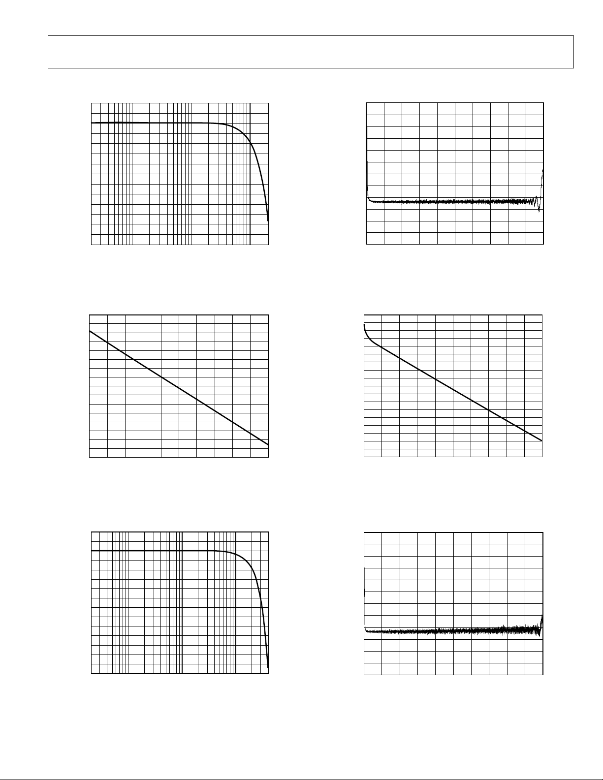
TYPICAL PERFORMANCE CHARACTERISTICS
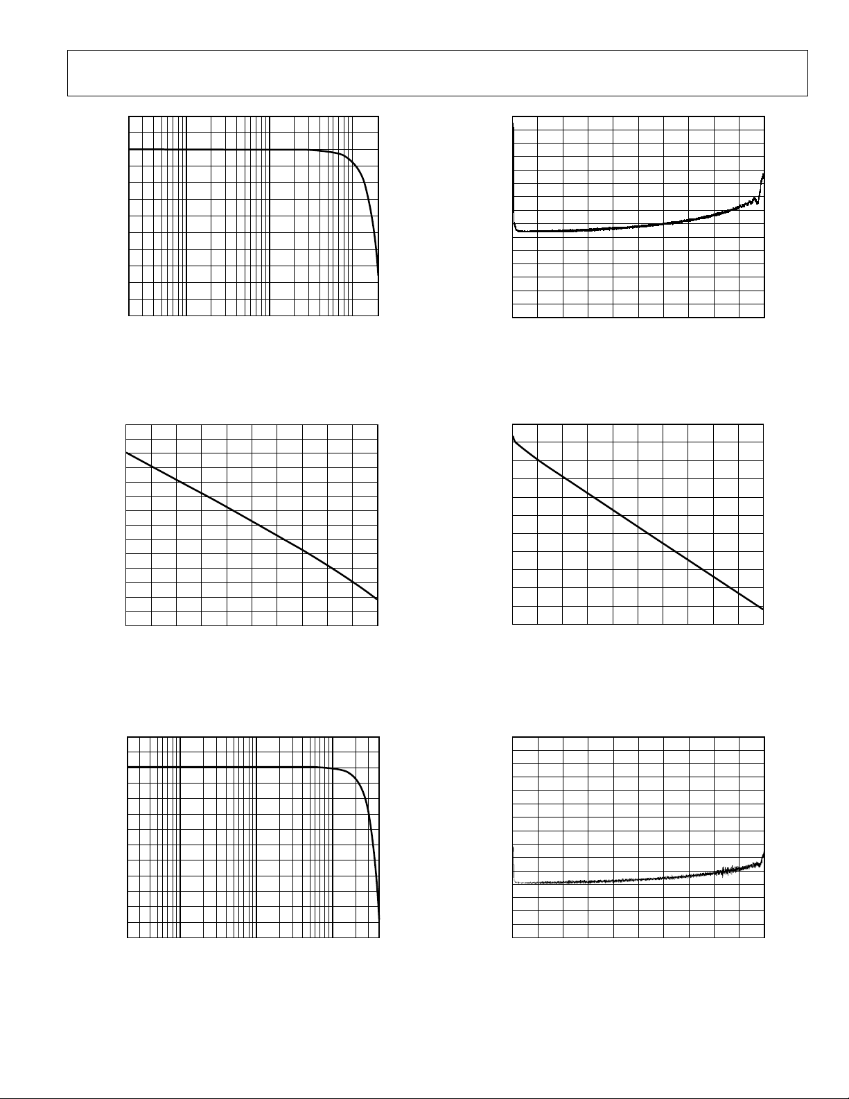
= 48 kHz, Signal Path = AIN0 to DSP (Without Processing) to LOUTLx
f
S
Figure 11. Phase vs. Frequency, 20 kHz Bandwidth,
= 48 kHz, Signal Path = AIN0 to DSP (Without Processing) to LOUTLx
f
S
Figure 10. Relative Level vs. Frequency,
= 48 kHz, Signal Path = AIN0 to DSP (Without Processing) to LOUTLx
f
S
Figure 14. Phase vs. Frequency, 2 kHz Bandwidth,
= 48 kHz, Signal Path = AIN0 to DSP (Without Processing) to LOUTLx
f
S
Figure 13. Group Delay vs. Frequency,
= 96 kHz, Signal Path = AIN0 to DSP (Without Processing) to LOUTLx
f
S
Figure 12. Relative Level vs. Frequency,
= 96 kHz, Signal Path = AIN0 to DSP (Without Processing) to LOUTLx
f
S
Rev. 0 | Page 17 of 116
Figure 15. Group Delay vs. Frequency,
ADAU1772 Data Sheet
50
–600
–550
–500
–450
–400
–350
–300
–250
–200
–150
–100
–50
0
0 4 8 12 16 20 24 28 32 36 40
PHASE (Degrees)
FREQUENCY ( kHz )
10804-015
1
–9
–8
–7
–6
–5
–4
–3
–2
–1
0
10k1k100
RELATIVE LEVEL (dB)
FREQUENCY ( Hz )
10804-016
200
–1300
–1200
–1100
–1000
–900
–800
–700
–600
–500
–400
–300
–200
–100
0
100
0 8070605040302010
PHASE (Degrees)
FREQUENCY ( kHz )
10804-017
6
–30
–28
–26
–24
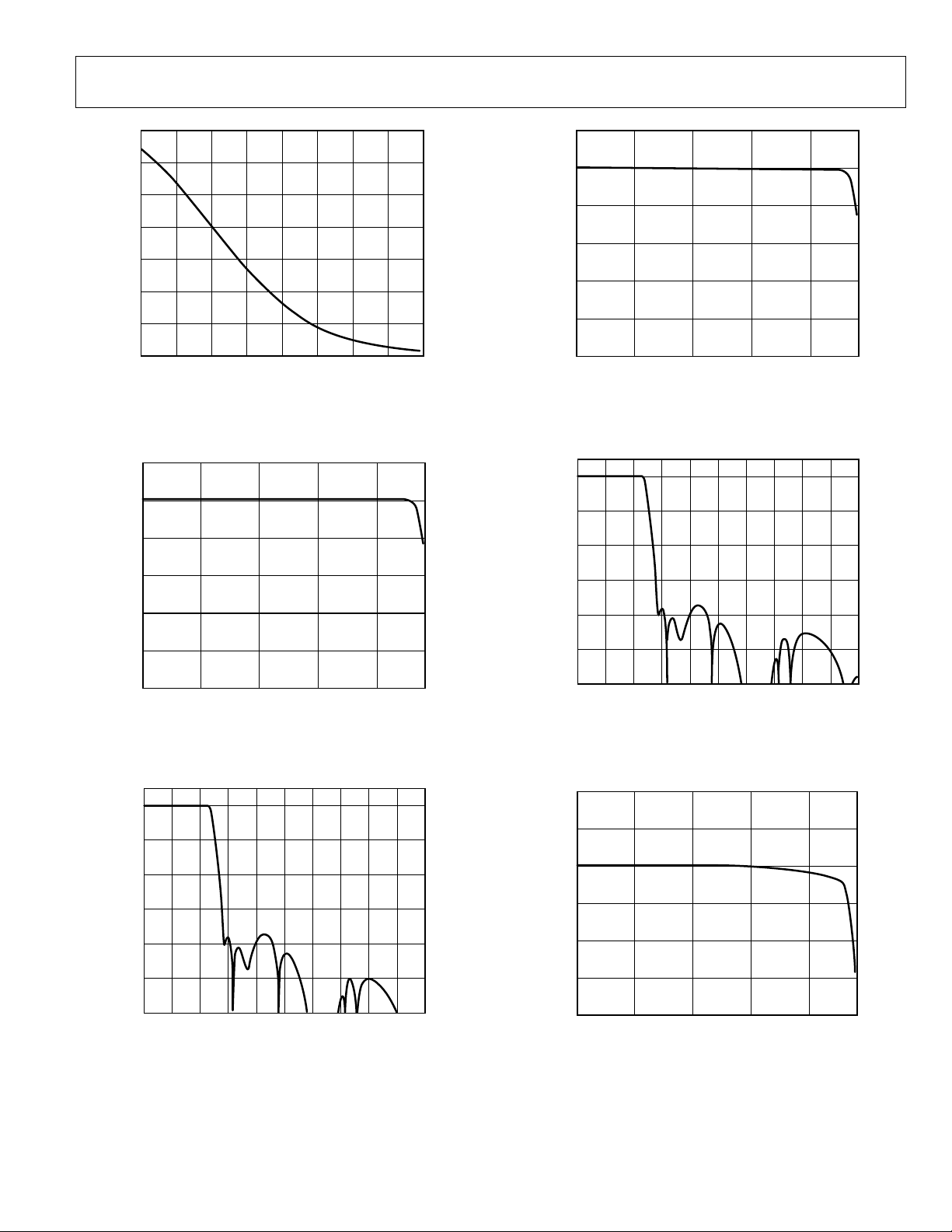
–22
–20
–18
–16
–14
–12
–10
–8
–6
–4
–2
0
2
4
0 0.2 0.4 0.6 0.8 1.0 1.2 1.4 1.6 1.8 2.0
PHASE (Degrees)
FREQUENCY ( kHz )
10804-018
120
0
10
20
30
40
50
60
70
80
90
100
110
0 10 20 30 40 50 60 70 80
GROUP DEL AY ( µ s)
FREQUENCY ( kHz )
10804-019
6
–30
–28
–26
–24
–22
–20
–18
–16
–14
–12
–10
–8
–6
–4
–2
0
2
4
0 0.2 0.4 0.6 0.8 1.0 1.2 1.4 1.6 1.8 2.0
PHASE (Degrees)
FREQUENCY ( kHz )
10804-020
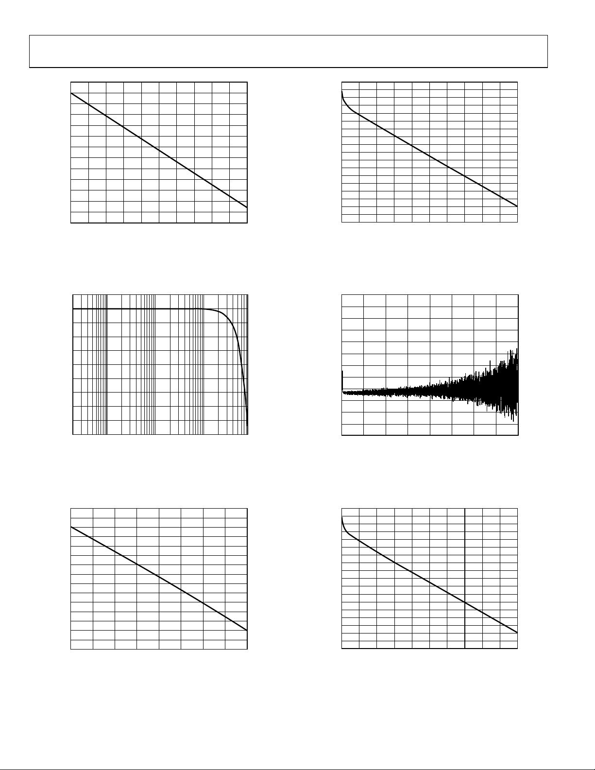
Figure 16. Phase vs. Frequency, 40 kHz Bandwidth,
= 96 kHz, Signal Path = AIN0 to DSP (Without Processing) to LOUTLx
f
S
Figure 17. Relative Level vs. Frequency,
= 192 kHz, Signal Path = AIN0 to DSP (Without Processing) to LOUTLx
f
S
Figure 19. Phase vs. Frequency, 2 kHz Bandwidth,
= 96 kHz, Signal Path = AIN0 to DSP (Without Processing) to LOUTLx
f
S
Figure 20. Group Delay vs. Frequency,
= 192 kHz, Signal Path = AIN0 to DSP (Without Processing) to LOUTLx
f
S
f
S
Figure 18. Phase vs. Frequency, 80 kHz Bandwidth,
= 192 kHz, Signal Path = AIN0 to DSP (Without Processing) to LOUTLx
= 192 kHz, Signal Path = AIN0 to DSP (Without Processing) to LOUTLx
f
S
Rev. 0 | Page 18 of 116
Figure 21. Phase vs. Frequency, 2 kHz Bandwidth,
Data Sheet ADAU1772
0.04
–0.20
–0.18
–0.16
–0.14
–0.12
–0.10
–0.08
–0.06
–0.04
–0.02
0
0.02
100 1k 10k
RELATIVE LEVEL (dB)
FREQUENCY ( Hz )
10804-021
200
–1200
–1100
–1000
–900
–800
–700
–600
–500
–400
–300
–200
–100
0
100
0 2 4 6 8 10 12 14 16 18 20
PHASE (Degrees)
FREQUENCY ( kHz )
10804-022
0.4
–2.2
–2.0
–1.8
–1.6
–1.4
–1.2
–1.0
–0.8
–0.6
–0.4
–0.2
0
0.2
100 1k 10k
RELATIVE LEVEL (dB)
FREQUENCY ( Hz )
10804-023
300
280
260
240
220
200
180
160
140
120
100
80
60
40
20
0
0 2 4 6 8 10 12 14 16 18 20
GROUP DEL AY ( µ s)
FREQUENCY ( kHz )
10804-024
10
–100
–90
–80
–70
–60
–50
–40
–30
–20
–10
0
0 0.2 0.4 0.6 0.8 1.0 1.2 1.4 1.6 1.8 2.0
PHASE (Degrees)
FREQUENCY ( kHz )
10804-025
300
280
260
240
220
200
180
160
140
120
100
80
60
40
20
0
0 4 8 12 16 20 24 28 32 36 40
GROUP DEL AY ( µ s)
FREQUENCY ( kHz )
10804-026
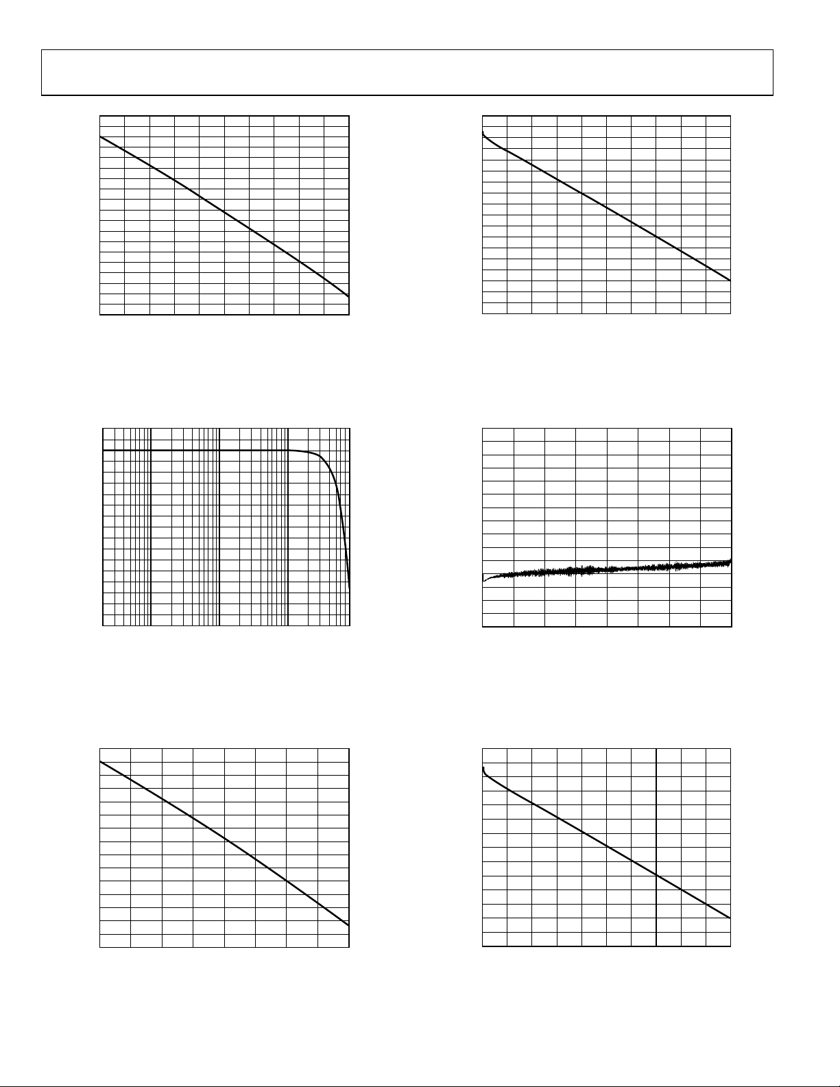
Figure 22. Relative Level vs. Frequency,
= 48 kHz, Signal Path = AIN0 to ASRC to ADC_SDATA0
f
S
Figure 23. Phase vs. Frequency, 20 kHz Bandwidth,
= 48 kHz, Signal Path = AIN0 to ASRC to ADC_SDATA0
f
S
Figure 25. Group Delay vs. Frequency,
= 48 kHz, Signal Path = AIN0 to ASRC to ADC_SDATA0
f
S
Figure 26. Phase vs. Frequency, 2 kHz Bandwidth,
= 48 kHz, Signal Path = AIN0 to ASRC to ADC_SDATA0
f
S
Figure 24. Relative Level vs. Frequency,
= 96 kHz, Signal Path = AIN0 to ASRC to ADC_SDATA0
f
S
Figure 27. Group Delay vs. Frequency,
= 96 kHz, Signal Path = AIN0 to ASRC to ADC_SDATA0
f
S
Rev. 0 | Page 19 of 116

ADAU1772 Data Sheet
200
–1500
–1400
–1300
–1200
–1100
–1000
–900
–800
–700
–600
–500
–400
–300
–200
–100
0
100
0 4 8 12 16 20 24 28 32 36 40
PHASE (Degrees)
FREQUENCY ( kHz )
10804-027
2
–22
–20
–18
–16
–14
–12
–10
–8
–6
–4
–2
0
10k100 1k
RELATIVE LEVEL (dB)
FREQUENCY ( Hz )
10804-028
200
–1800
–1600
–1400
–1200
–1000
–800
–600
–400
–200
0
800 10 20 30 40 50 60 70
PHASE (Degrees)
FREQUENCY ( kHz )
10804-029
10
–70
–65
–60
–55
–50
–45
–40
–35
–30
–25
–20
–15
–10
–5
0
5
0 0.2 0.4 0.6 0.8 1.0 1.2 1.4 1.6 1.8 2.0
PHASE (Degrees)
FREQUENCY ( kHz )
10804-030
300
0
20
40
60
80
100
120
140
160
180
220
260
280
200
240
0 10 20 30 40 50 60 70 80
GROUP DEL AY ( µ s)
FREQUENCY ( kHz )
10804-031
10
–40
–35
–30
–25
–20
–15
–10
–5
0
5
0 0.2 0.4 0.6 0.8 1.0 1.2 1.4 1.6 1.8 2.0
PHASE (Degrees)
FREQUENCY ( kHz )
10804-032
Figure 28. Phase vs. Frequency, 40 kHz Bandwidth,
= 96 kHz, Signal Path = AIN0 to ASRC to ADC_SDATA0
f
S
Figure 29. Relative Level vs. Frequency,
= 192 kHz, Signal Path = AIN0 to ASRC to ADC_SDATA0
f
S
Figure 31. Phase vs. Frequency, 2 kHz Bandwidth,
= 96 kHz, Signal Path = AIN0 to ASRC to ADC_SDATA0
f
S
Figure 32. Group Delay vs. Frequency,
= 192 kHz, Signal Path = AIN0 to ASRC to ADC_SDATA0
f
S
Figure 30. Phase vs. Frequency, 80 kHz Bandwidth,
= 192 kHz, Signal Path = AIN0 to ASRC to ADC_SDATA0
f
S
Figure 33. Phase vs. Frequency, 2 kHz Bandwidth,
= 192 kHz, Signal Path = AIN0 to ASRC to ADC_SDATA0
f
S
Rev. 0 | Page 20 of 116

Data Sheet ADAU1772
0.02
–0.10
–0.09
–0.08
–0.07
–0.06
–0.05
–0.04
–0.03
–0.02
–0.01
0
0.01
100 1k 10k
RELATIVE LEVEL (dB)
FREQUENCY ( Hz )
10804-033
200
–1300
–1200
–1100
–1000
–900
–800
–700
–600
–500
–400
–300
–200
100
0
–100
PHASE (Degrees)
FREQUENCY ( kHz )
0 2 4 6 8 10 12 14 16 18 20
10804-034
0.2
–0.9
–0.8
–0.7
–0.6
–0.5
–0.4
–0.3
–0.2
–0.1
0
0.1
100 1k 10k
RELATIVE LEVEL (dB)
FREQUENCY ( Hz )
10804-035
300
0
20
40
60
80
100
120
140
160
180
200
220
240
260
280
GROUP DEL AY ( µ s)
FREQUENCY ( kHz )
0 2 4 6 8 10 12 14 16 18 20
10804-036
10
–120
–110
–100
–90
–80
–70
–60
–50
–40
–30
–20
0
–10
PHASE (Degrees)
FREQUENCY ( kHz )
0 0.2 0.4 0.6 0.8 1.0 1.2 1.4 1.6 1.8 2.0
10804-037
300
0
20
40
60
80
100
120
140
160
180
200
220
240
260
280
GROUP DEL AY ( µ s)
FREQUENCY ( kHz )
0 4 8 12 16 20 24 28 32 36 40
10804-038
Figure 34. Relative Level vs. Frequency,
= 48 kHz, Signal Path = DAC_SDATA to ASRC to LOUTLx
f
S
Figure 35. Phase vs. Frequency, 20 kHz Bandwidth,
= 48 kHz, Signal Path = DAC_SDATA to ASRC to LOUTLx
f
S
Figure 37. Group Delay vs. Frequency,
= 48 kHz, Signal Path = DAC_SDATA to ASRC to LOUTLx
f
S
Figure 38. Phase vs. Frequency, 2 kHz Bandwidth,
= 48 kHz, Signal Path = DAC_SDATA to ASRC to LOUTLx
f
S
Figure 36. Relative Level vs. Frequency,
= 96 kHz, Signal Path = DAC_SDATA to ASRC to LOUTLx
f
S
Figure 39. Group Delay vs. Frequency,
= 96 kHz, Signal Path = DAC_SDATA to ASRC to LOUTLx
f
S
Rev. 0 | Page 21 of 116
ADAU1772 Data Sheet
200
–1700
–1600
–1500
–1400
–1300
–1200
–1100
–1000
–900
–800
–700
–600
–500
–400
–300
–200
–100
0
100
PHASE (Degrees)
FREQUENCY ( kHz )
0 4 8 12 16 20 24 28 32 36 40
10804-039
1.0
–8.0
–7.5
–7.0
–6.5
–6.0
–5.5
–5.0
–4.5
–4.0
–3.5
–3.0
–2.5
–2.0
–1.5
–1.0
–0.5
0
0.5
RELATIVE LEVEL (dB)
FREQUENCY ( Hz )
100 1k 10k
10804-040
200
–2800
–2600
–2400
–2200
–2000
–1800
–1600
–1400
–1200
–1000
–600
–200
0
–800
–400
0 10 20 30 40 50 60 70 80
PHASE (Degrees)
FREQUENCY ( kHz )
10804-041
10
–80
–75
–70
–65
–60
–55
–50
–45
–40
–35
–30
–25
–20
–15
–10
–5
0
5
PHASE (Degrees)
FREQUENCY ( kHz )
0 0.2 0.4 0.6 0.8 1.0 1.2 1.4 1.6 1.8 2.0
10804-042
300
0
20
40
60
80
100
120
140
160
180
200
220
240
260
280
800 10 20 30 40 50 60 70
GROUP DEL AY ( µ s)
FREQUENCY ( kHz )
10804-043
10
–60
–55
–50
–45
–40
–35
–30
–25
–20
–15
–10
–5
0
5
PHASE (Degrees)
FREQUENCY ( kHz )
0 0.2 0.4 0.6 0.8 1.0 1.2 1.4 1.6 1.8 2.0
10804-044
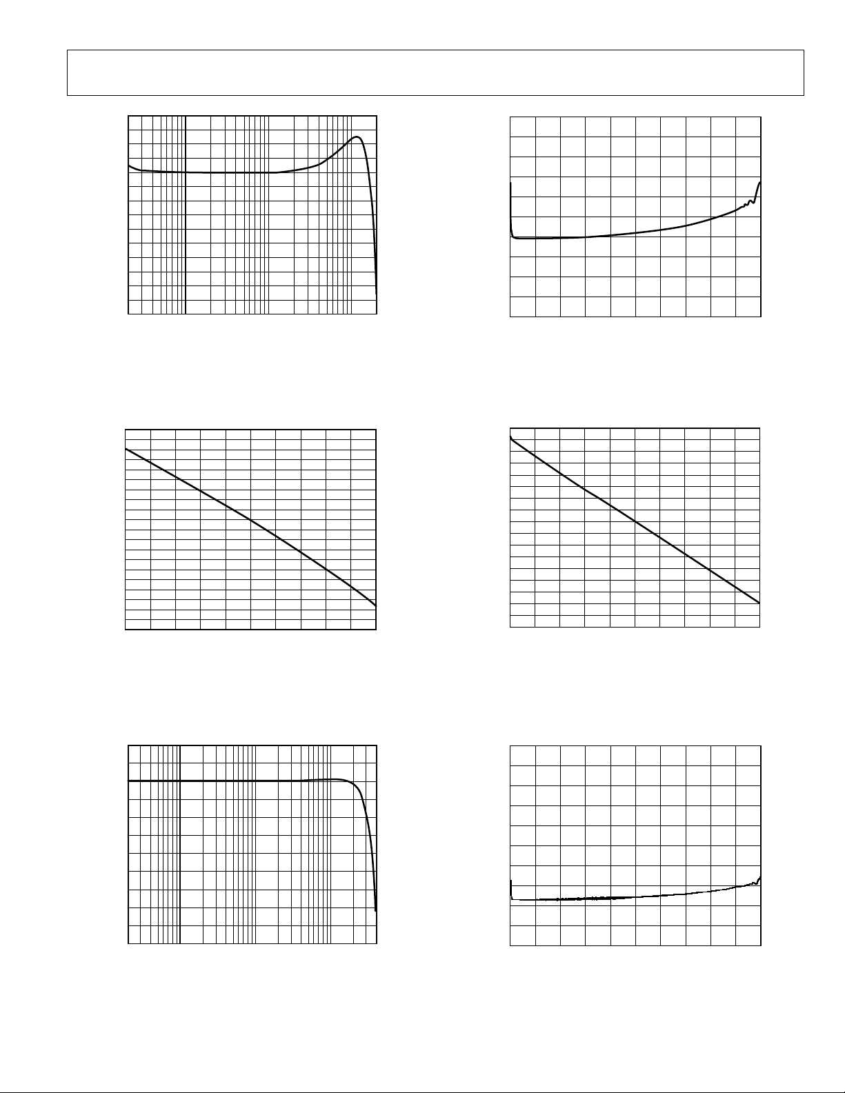
Figure 40. Phase vs. Frequency, 40 kHz Bandwidth,
= 96 kHz, Signal Path = DAC_SDATA to ASRC to LOUTLx
f
S
Figure 41. Relative Level vs. Frequency,
= 192 kHz, Signal Path = DAC_SDATA to ASRC to LOUTLx
f
S
Figure 43. Phase vs. Frequency, 2 kHz Bandwidth,
= 96 kHz, Signal Path = DAC_SDATA to ASRC to LOUTLx
f
S
Figure 44. Group Delay vs. Frequency,
= 192 kHz, Signal Path = DAC_SDATA to ASRC to LOUTLx
f
S
Figure 42. Phase vs. Frequency, 80 kHz Bandwidth,
= 192 kHz, Signal Path = DAC_SDATA to ASRC to LOUTLx
f
S
Figure 45. Phase vs. Frequency, 2 kHz Bandwidth,
= 192 kHz, Signal Path = DAC_SDATA to ASRC to LOUTLx
f
S
Rev. 0 | Page 22 of 116
Data Sheet ADAU1772
0.020
–0.050
–0.045
–0.040
–0.035
–0.030
–0.025
–0.020
–0.015
–0.010
–0.005
0
0.005
0.010
0.015
100 1k 10k
RELATIVE LEVEL (dB)
FREQUENCY ( Hz )
10804-045
200
–1300
–1400
–1500
–1600
–1700
–1800
–1200
–1100
–1000
–900
–800
–700
–600
–500
–400
–300
–200
100
0
–100
PHASE (Degrees)
FREQUENCY ( kHz )
0 2 4 6 8 10 12 14 16 18 20
10804-046
0.4
–1.8
–1.6
–1.4
–1.2
–1.0
–0.8
–0.6
–0.4
–0.2
0
0.2
100 1k 10k
RELATIVE LEVEL (dB)
FREQUENCY ( Hz )
10804-047
500
0
50
100
150
200
250
300
350
400
450
GROUP DEL AY ( µ s)
FREQUENCY ( kHz )
0 2 4 6 8 10 12 14 16 18 20
10804-048
10
–160
–150
–140
–130
–120
–110
–100
–90
–80
–70
–60
–50
–40
–30
–20
–10
0
PHASE (Degrees)
FREQUENCY ( kHz )
0 0.2 0.4 0.6 0.8 1.0 1.2 1.4 1.6 1.8 2.0
10804-049
500
450
400
350
300
250
200
150
100
50
0
GROUP DEL AY ( µ s)
FREQUENCY ( kHz )
0 4 8 12 16 20 24 28 32 36 40
10804-050
= 48 kHz, Signal Path = DAC_SDATA to ASRC to DSP (Without Processing)
f
S
to ASRC to ADC_SDATA0
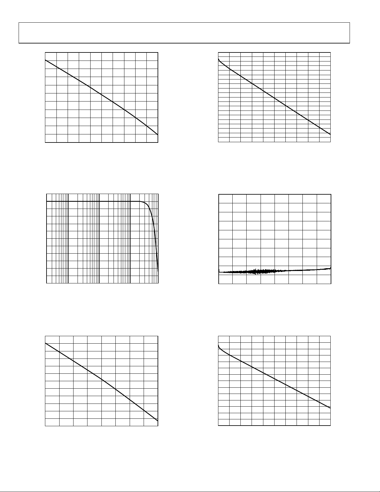
Figure 47. Phase vs. Frequency, 20 kHz Bandwidth,
Figure 46. Relative Level vs. Frequency,
= 48 kHz, Signal Path = DAC_SDATA to ASRC to DSP (Without Processing)
f
S
to ASRC to ADC_SDATA0
= 48 kHz, Signal Path = DAC_SDATA to ASRC to DSP (Without Processing)
f
S
to ASRC to ADC_SDATA0
Figure 50. Phase vs. Frequency, 2 kHz Bandwidth,
Figure 49. Group Delay vs. Frequency,
= 48 kHz, Signal Path = DAC_SDATA to ASRC to DSP (Without Processing)
f
S
to ASRC to ADC_SDATA0
= 96 kHz, Signal Path = DAC_SDATA to ASRC to DSP (Without Processing)
f
S
Figure 48. Relative Level vs. Frequency,
to ASRC to ADC_SDATA0
= 96 kHz, Signal Path = DAC_SDATA to ASRC to DSP (Without Processing)
f
S
to ASRC to ADC_SDATA0
Rev. 0 | Page 23 of 116
Figure 51. Group Delay vs. Frequency,
ADAU1772 Data Sheet
200
–2000
–1800
–1600
–1400
–1200
–1000
–800
–600
–400
–200
0
PHASE (Degrees)
FREQUENCY ( kHz )
0 4 8 12 16 20 24 28 32 36 40
10804-051
2
–22
–20
–18
–16
–14
–12
–10
–8
–6
–4
–2
0
RELATIVE LEVEL (dB)
FREQUENCY ( Hz )
100 1k 10k
10804-052
200
–2200
–2000
–1800
–1600
–1400
–1200
–1000
–800
–600
–400
–200
0
800 10 20 30 40 50 60 70
PHASE (Degrees)
FREQUENCY ( kHz )
10804-053
10
–60
–65
–70
–75
–80
–85
–90
–55
–50
–45
–40
–35
–30
–25
–20
–15
–10
–5
0
5
PHASE (Degrees)
FREQUENCY ( kHz )
0 0.2 0.4 0.6 0.8 1.0 1.2 1.4 1.6 1.8 2.0
10804-054
500
0
50
100
150
200
250
300
350
400
450
800 10 20 30 40 50 60 70
GROUP DEL AY ( µ s)
FREQUENCY ( kHz )
10804-055
10
–60
–55
–50
–45
–40
–35
–30
–25
–20
–15
–10
–5
0
5
PHASE (Degrees)
FREQUENCY ( kHz )
0 0.2 0.4 0.6 0.8 1.0 1.2 1.4 1.6 1.8 2.0
10804-056
= 96 kHz, Signal Path = DAC_SDATA to ASRC to DSP (Without Processing)
f
S
to ASRC to ADC_SDATA0
Figure 53. Relative Level vs. Frequency,
Figure 52. Phase vs. Frequency, 40 kHz Bandwidth,
= 192 kHz, Signal Path = DAC_SDATA to ASRC to DSP (Without Processing)
f
S
to ASRC to ADC_SDATA0
= 96 kHz, Signal Path = DAC_SDATA to ASRC to DSP (Without Processing)
f
S
to ASRC to ADC_SDATA0
Figure 56. Group Delay vs. Frequency,
Figure 55. Phase vs. Frequency, 2 kHz Bandwidth,
= 192 kHz, Signal Path = DAC_SDATA to ASRC to DSP (Without Processing)
f
S
to ASRC to ADC_SDATA0
= 192 kHz, Signal Path = DAC_SDATA to ASRC to DSP (Without Processing)
f
S
Figure 54. Phase vs. Frequency, 80 kHz Bandwidth,
to ASRC to ADC_SDATA0
= 192 kHz, Signal Path = DAC_SDATA to ASRC to DSP (Without Processing)
f
S
to ASRC to ADC_SDATA0
Rev. 0 | Page 24 of 116
Figure 57. Phase vs. Frequency, 2 kHz Bandwidth,
Data Sheet ADAU1772
35
30
25
20
15
10
5
0
INPUT IMPEDANCE (kΩ)
PGA GAIN SETTING (dB)
–12 –6 0 6 12 18 24 30 36
10804-057
2
–10
–8
–6
–4
–2
0
0 2015105
10804-100
MAGNITUDE ( dBFS)
FREQUENCY ( kHz )
–120
–100
–80
–60
–40
–20
0
0 100908070605040302010
10804-101
MAGNITUDE ( dBFS)
FREQUENCY ( kHz )
2
–10
–8
–6
–4
–2
0
0 2015105
10804-102
MAGNITUDE ( dBFS)
FREQUENCY ( kHz )
–120
–100
–80
–60
–40
–20
0
0 100908070605040302010
10804-103
MAGNITUDE ( dBFS)
FREQUENCY ( kHz )
2
–4
–3
–2
–1
0
1
0 2015105
10804-104
MAGNITUDE ( dBFS)
FREQUENCY ( kHz )
Figure 58. Input Impedance vs. PGA Gain
(see the Input Impedance section)
Figure 59. Decimation Pass-Band Response, fS = 96 kHz
Figure 61. Decimation Pass-Band Response, fS = 192 kHz
Figure 62. Total Decimation Response, f
= 192 kHz
S
Figure 60. Total Decimation Response, fS = 96 kHz
Figure 63. Interpolation Pass-Band Response, fS = 96 kHz
Rev. 0 | Page 25 of 116
ADAU1772 Data Sheet
–120
–100
–80
–60
–40
–20
0
0 100908070605040302010
10804-105
MAGNITUDE ( dBFS)
FREQUENCY ( kHz )
2
–4
–3
–2
–1
0
1
MAGNITUDE ( dBFS)
FREQUENCY ( kHz )
0 2015105
10804-106
–120
–100
–80
–60
–40
–20
0
0 10987654321
10804-107
MAGNITUDE ( dBFS)
FREQUENCY ( kHz )
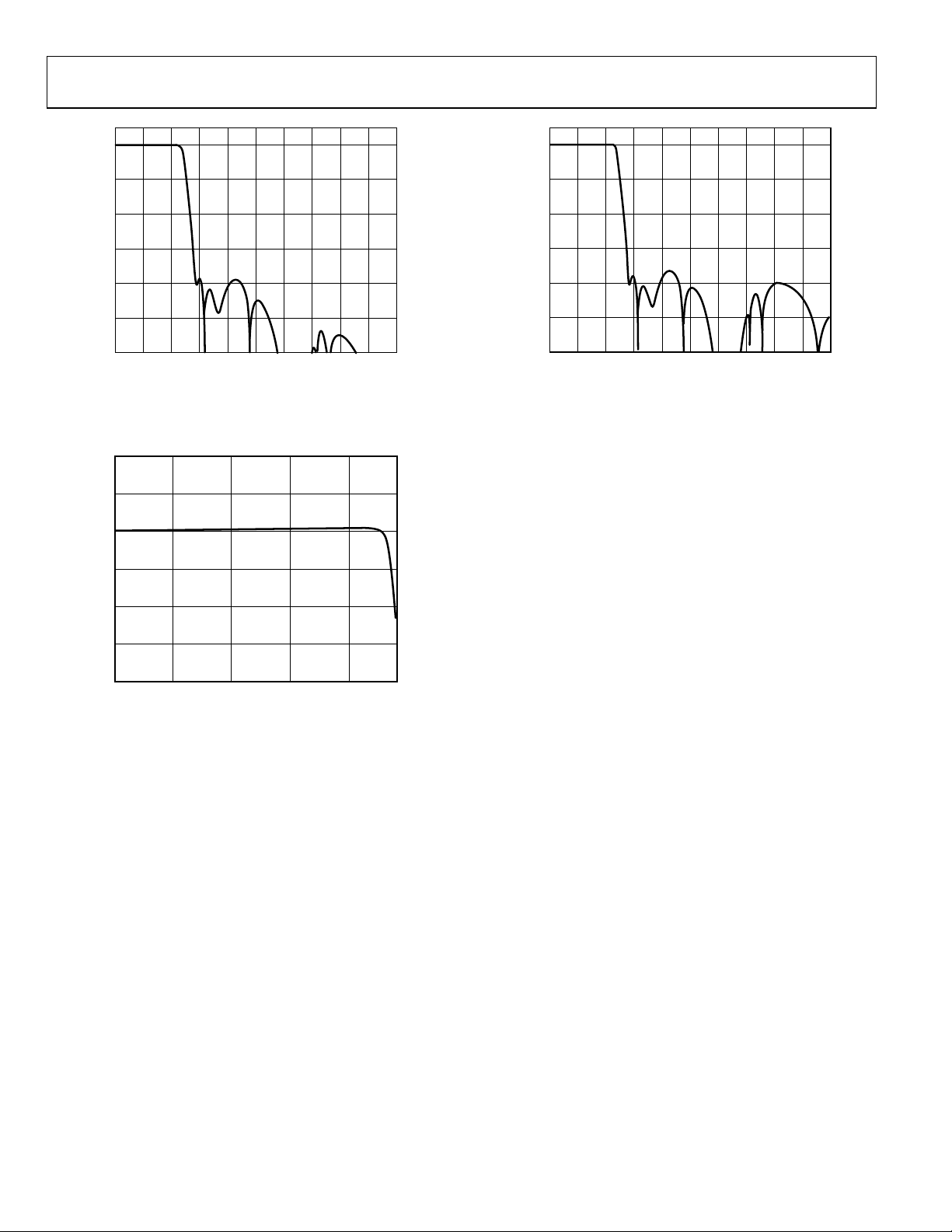
Figure 64. Total Interpolation Response, fS = 96 kHz
Figure 65. Interpolation Pass-Band Response, fS = 192 kHz
Figure 66. Total Interpolation Response, fS = 192 kHz
Rev. 0 | Page 26 of 116
ADAU1772 Data Sheet
EEPROM
CONTROL INTERFACE:
SWITCHE S AND
POTENTIOMETERS
DC VOLTAGE SOURCE:
1.8 V TO 3.3 V
LEFT
MICROPHONE
RIGHT
MICROPHONE
LEFT HE ADP HONE
RIGHT HEADP HONE
1
SDA/MISO
2
SCL/SCLK
3
ADDR1/MOSI
4
ADDR0/SS
5
SELFBOOT
6
MICBIAS0
7
MICBIAS1
8
AIN0REF
9
AIN0
10
AVDD
11
13
AIN1REF
14
AIN1
15
AIN2REF
16
AIN2
12
CM
17
AIN3REF
18
AIN3
19
AVDD
20
23
AGND
AGND
AGND
DGND
24
AVDD
21
HPOUTLN/LOUTLN
22
HPOUTLP/LOUTLP
25
HPOUTRN/LOUTRN
26
HPOUTRP/LOUTRP
27
PD
40
IOVDD
28
REG_OUT
30
31
LRCLK/MP3
32
BCLK/MP2
33
DAC_SDATA/MP0
34
ADC_SDATA0/PDMOUT/MP1
38
XTALO
39
XTALI/MCLKIN
35
ADC_SDATA1/CLKOUT/MP6
36
DMIC2_3/MP5
37
DMIC0_1/MP4
29
DVDD
41
EP
ADAU1772
10µF
10µF
+
10µF
0.10µF
100Ω
22pF
22pF
+
10µF
0.10µF
+
10µF
0.10µF
0.10µF
0.10µF
0.10µF
47µF
47µF
2kΩ 2kΩ
1.0µF
LEFT_AUDIO
RIGHT_AUDIO
10804-060
SYSTEM BLOCK DIAGRAMS
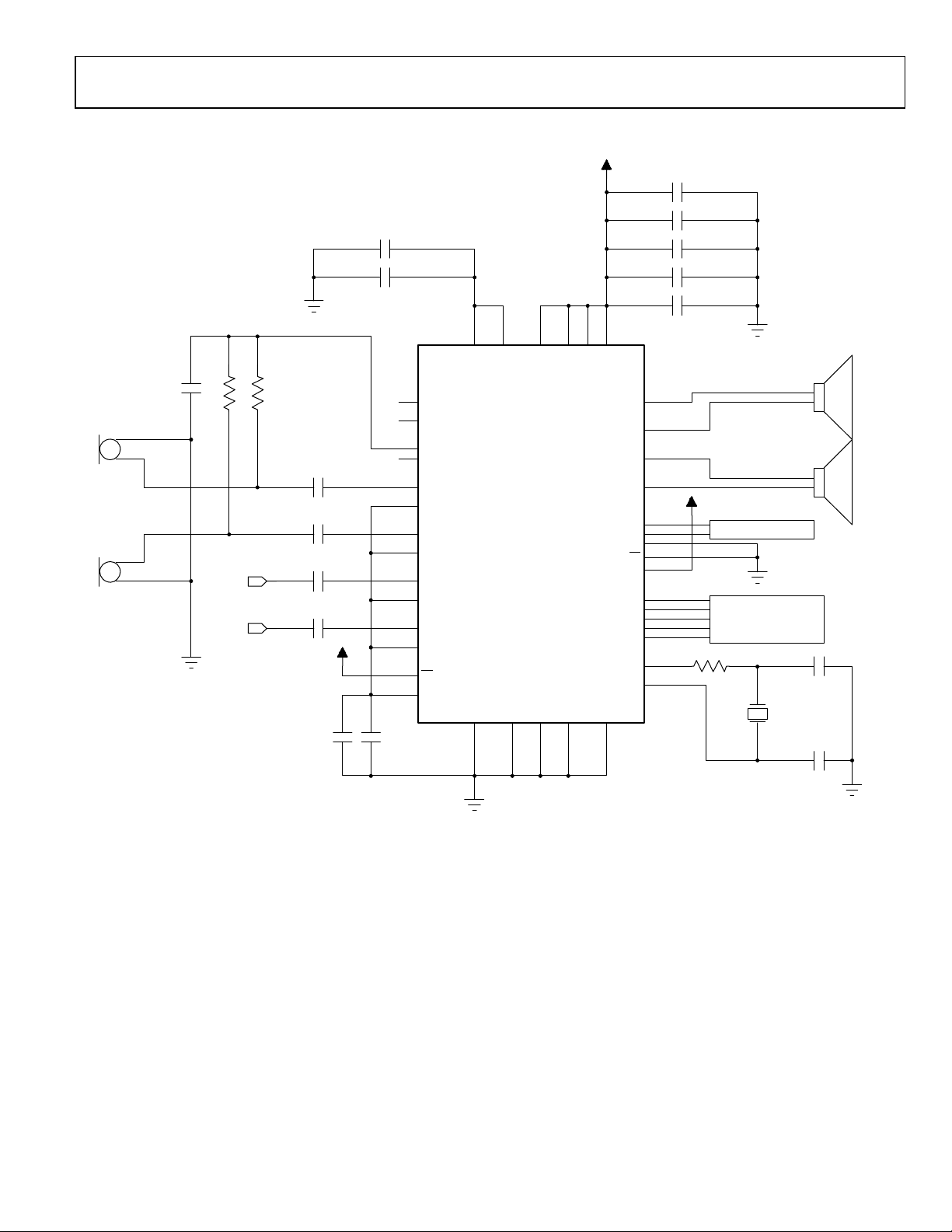
Figure 67. ADAU1772 System Block Diagram with Analog Microphones, Self-Boot Mode
Rev. 0 | Page 27 of 116

ADAU1772 Data Sheet
THEORY OF OPERATION
The ADAU1772 is a low power audio codec with an optimized
audio processing core, making it ideal for noise cancelling
applications that require high quality audio, low power, small
size, and low latency. The four ADC and two DAC channels
each have an SNR of at least +96 dB and a THD + N of at least
−88 dB. The serial data port is compatible with I
right justified, and TDM modes, with tristating for interfacing
to digital audio data. The operating voltage range is 1.8 V to
3.63 V, w i t h a n o n-board regulator generating the internal
digital supply voltage. If desired, the regulator can be powered
down and the voltage can be supplied externally.
The input signal path includes flexible configurations that can
accept single-ended analog microphone inputs as well as up to
four digital microphone inputs. Two microphone bias pins provide
seamless interfacing to electret microphones. Each input signal
has its own programmable gain amplifier (PGA) for volume
adjustment.
The ADCs and DACs are high quality, 24-bit Σ-Δ converters
that operate at a selectable 192 kHz or 96 kHz sampling rate.
The ADCs have an optional high-pass filter with a cutoff
frequency of 1 Hz, 4 Hz, or 8 Hz. The ADCs and DACs also
include very fine-step digital volume controls.
The stereo DAC output is capable of differentially driving a
headphone earpiece speaker with 16 Ω impedance or higher.
One side of the differential output can be powered down if
single-ended operation is required. There is also the option to
change to line output mode when the output is lightly loaded.
The core has a reduced instruction set that optimizes this codec
for noise cancellation. The program and parameter RAMs can
be loaded with custom audio processing signal flow built using
the SigmaStudio™ graphical programming software from
Analog Devices, Inc. The values stored in the parameter RAM
2
S, left justified,
control individual signal processing blocks. The ADAU1772 also
has a self-boot function that can be used to load the program
and parameter RAM along with the register settings on powerup using an external EEPROM.
The SigmaStudio software is used to program and control the core
through the control port. Along with designing and tuning a signal
flow, the tools can be used to configure all of the ADAU1772
registers. The SigmaStudio graphical interface allows anyone with
digital or analog audio processing knowledge to easily design the
DSP signal flow and port it to a target application. The interface
also provides enough flexibility and programmability for an
experienced DSP programmer to have in-depth control of the
design. In SigmaStudio, the user can connect graphical blocks
(such as biquad filters, volume controls, and arithmetic operations),
compile the design, and load the program and parameter files into
the ADAU1772 memory through the control port. SigmaStudio
also allows the user to download the design to an external EEPROM
for self-boot operation. Signal processing blocks available in the
provided libraries include the following:
• Single-precision biquad filters
• Second order filters
• Absolute value and two-input adder
• Volume controls
• Limiter
The ADAU1772 can generate its internal clocks from a wide range
of input clocks by using the on-board fractional PLL. The PLL
accepts inputs from 8 MHz to 27 MHz. For standalone operation,
the clock can be generated using the on-board crystal oscillator.
The ADAU1772 is provided in a small, 40-lead, 6 mm × 6 mm
LFCSP with an exposed bottom pad.
Rev. 0 | Page 28 of 116
Data Sheet ADAU1772
MCLK ÷X
× (R + N/M)
TO PLL
CLOCK DIVIDER
10804-061
SYSTEM CLOCKING AND POWER-UP
CLOCK INITIALIZATION
The ADAU1772 can generate its clocks either from an externally
provided clock or from a crystal oscillator. In both cases, the onboard PLL can be used or the clock can be fed directly to the
core. When a crystal oscillator is used, it is desirable to use a
12.288 MHz crystal, and the crystal oscillator function must be
enabled in the COREN bit (Address 0x0000). If the PLL is used,
it should always be set to output 24.576 MHz. The PLL can be
bypassed if a clock of 12.288 MHz or 24.576 MHz is available in
the system. Bypassing the PLL saves system power.
The CC_MDIV and CC_CDIV bits should not be changed after
setup, but the CLKSRC bit can be switched while the core is
running.
The CC_MDIV and CC_CDIV bits should be set so that the core
and internal master clock are always 12.288 MHz; for example,
when using a 24.576 MHz external source clock or if using the
PLL, it is necessary to use the internal divide by 2 (see Ta ble 11).
Table 11. Clock Configuration Settings
CC_MDIV CC_CDIV Description
1 1 Divide PLL/external clock by 1. Use these
settings for a 12.288 MHz direct input clock
source.
0 0 Divide PLL/external clock by 2. Use these
settings for a 24.576 MHz direct input clock
source or if using the PLL.
PLL Bypass Setup
On power up, the ADAU1772 comes out of an internal reset
after 12 ms. The rate of the internal master clock must be set
properly using the CC_MDIV bit in the clock control register
(Address 0x0000). When bypassing the PLL, the clock associated
with MCLKIN must be either 12.288 MHz or 24.576 MHz. The
internal master clock of the ADAU1772 is disabled until the
COREN bit is asserted.
PLL Enabled Setup
The core clock of the ADAU1772 is disabled by the default
setting of Bit COREN and should remain disabled during the
PLL lock acquisition period. The user can poll the LOCK bit to
determine when the PLL has locked. After lock is acquired, the
ADAU1772 can be started by asserting the COREN bit. This bit
enables the core clock for all the internal blocks of the ADAU1772.
To program the PLL during initialization or reconfiguration of
the codec, the following procedure must be followed:
1. Ensure that PLL_EN (Bit 7, Address 0x0000) is set low.
2. Set/reset the PLL control registers (Address 0x0001 to
Address 0x0005).
3. Enable the PLL using the PLL_EN bit.
4. Poll the PLL lock bit in Register 0x0006.
5. Set the COREN bit in Register 0x0000 after PLL lock is
acquired.
Control Port Access During Initialization
During the lock acquisition period, only Register 0x0000 to
Register 0x0006 are accessible through the control port. A read
or write to any other register is prohibited until the core clock
enable bit and the lock bit are both asserted.
After the CORE_RUN bit (Address 0x0009) is set high, the
DAC_SOURCE0 and DAC_SOURCE1 register bits should not
be changed. If these bits must be changed after the ADAU1772
is running, the CORE_RUN bit first must be disabled.
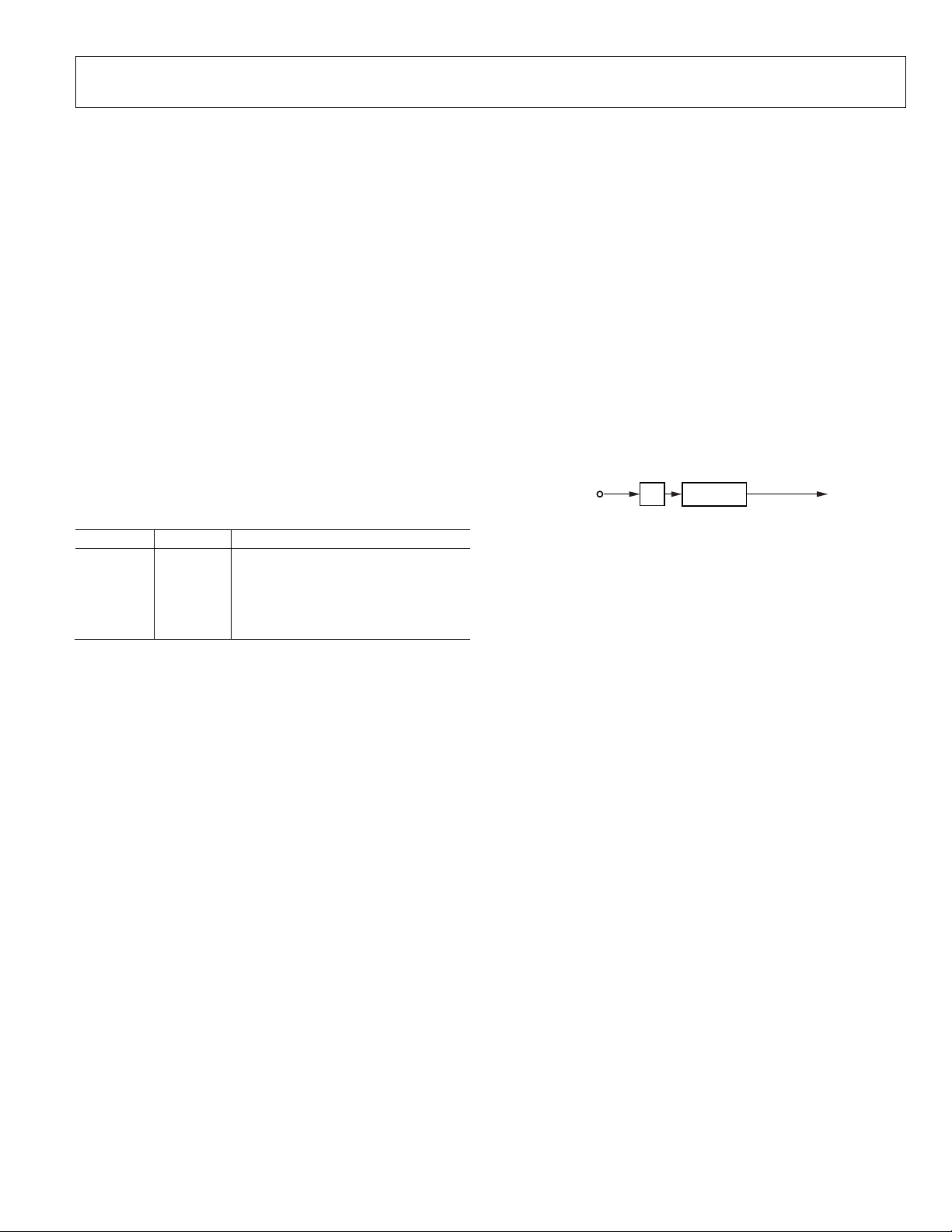
PLL
The PLL uses the MCLKIN signal as a reference to generate
the core clock. The PLL settings are set in Register 0x0000 to
Register 0x0005. Depending on the MCLK frequency, the PLL
must be set for either integer or fractional mode. The PLL can
accept input frequencies in the range of 8 MHz to 27 MHz.
Figure 68. PLL Block Diagram
Input Clock Divider
Before reaching the PLL, the input clock signal goes through an
integer clock divider to ensure that the clock frequency is within
a suitable range for the PLL. The X bits in the PLL_CTRL4 register
(Bits[2:1], Address 0x0005) sets the PLL input clock divide ratio.
Integer Mode
Integer mode is used when the clock input is an integer multiple
of the PLL output.
For example, if MCLKIN = 12.288 MHz and (X + 1) = 1, and
f
= 48 kHz, then
S
PLL Required Output = 24.576 MHz
R/2 = 24.576 MHz/12.288 MHz = 2
where R/2 = 2 or R = 4.
In integer mode, the values set for N and M are ignored.
Tabl e 12 lists common integer PLL parameter settings for
48 kHz sampling rates.
Fractional Mode
Fractional mode is used when the clock input is a fractional
multiple of the PLL output.
For example, if MCLKIN = 13 MHz, (X + 1) = 1, and
f
= 48 kHz, then
S
PLL Required Output = 24.576 MHz
(1/2) × (R + (N/M)) = 24.576 MHz/13 MHz = (1/2) × (3 +
(1269/1625))
where:
R = 3.
N = 1269.
M = 1625.
Rev. 0 | Page 29 of 116
ADAU1772 Data Sheet
26 2 3
1625
1269
0x1B
0xF5
0x04
0x59
0x06
Tabl e 13 lists common fractional PLL parameter settings for
48 kHz sampling rates. When the PLL is used in fractional
mode, it is very important that the N/M fraction be kept in
the range of 0.1 to 0.9 to ensure correct operation of the PLL.
The PLL can output a clock in the range of 20.5 MHz to 27 MHz,
which should be taken into account when calculating PLL values
and MCLK frequencies.
CLOCK OUTPUT
The CLKOUT pin can be used as a master clock output to clock
other ICs in the system or as the clock for the digital microphone
inputs and PDM output. This clock can be generated from the
12.288 MHz master clock of the ADAU1772 by factors of 2, 1,
½, ¼, and ⅛. If PDM mode is enabled, only ½, ¼, and ⅛ settings
produce a clock signal on CLKOUT. The factor of 2 multiplier
works properly only if the input clock was previously divided by
2 using the CC_MDIV bit.
POWER SEQUENCING
AVDD and IOVDD can each be set to any voltage between 1.8 V
and 3.3 V, and DVDD can be set between 1.1 V and 1.8 V or
between 1.1 V and 1.2 V if using the on-board regulator.
On power-up, AVDD must be powered up before or at the same
time as IOVDD. IOVDD should not be powered up when power is
not applied to AVDD.
Enabling the
Before enabling
pin powers down all analog and digital circuits.
PD
(that is, setting it low), be sure to mute the
PD
outputs to avoid any pops when the IC is powered down.
can be tied directly to IOVDD for normal operation.
PD
Power-Down Considerations
When powering down the ADAU1772, be sure to mute the outputs
before AVDD power is removed; otherwise, pops or clicks may
be heard. The easiest way to achieve this is to use a regulator that
has a power good (PGOOD) signal to power the ADAU1772 or
generate a power good signal using additional circuitry external
to the regulator itself. Typically, on such regulators the power good
signal changes state when the regulated voltage drops below ~90%
of its target value. This power good signal can be connected to one
of the ADAU1772 multipurpose pins and used to mute the DAC
outputs by setting the multipurpose pin functionality to mute
both DACs in Register 0x0038 to Register 0x003E. This ensures
that the outputs are muted before power is completely removed.
Table 12. Integer PLL Parameter Settings for PLL Output = 24.576 MHz
Input Divider
MCLK Input (MHz)
12.288 1 4 Don’t care Don’t care 0x20
24.576 1 2 Don’t care Don’t care 0x10
(X + 1) Integer (R) Denominator (M) Numerator (N)
PLL_CTRL4 Settings
(Address 0x0005)
Table 13. Fractional PLL Parameter Settings for PLL Output = 24.576 MHz
PLL_CTRL[4:0] Settings
MCLK
Input
(MHz)
8 1 6 125 18 0x31 0x12 0x00 0x7D 0x00
13 1 3 1625 1269 0x19 0xF5 0x04 0x59 0x06
14.4 2 6 75 62 0x33 0x3E 0x00 0x4B 0x00
19.2 2 5 25 3 0x2B 0x03 0x00 0x19 0x00
27 2 3 1125 721 0x1B 0xD1 0x02 0x65 0x04
Input
Divider
(X + 1)
Integer
(R)
Denominator
(M)
Numerator
(N)
PLL_CTRL4
(0x0005)
(Address 0x0005 to Address 0x0001)
PLL_CTRL3
(0x0004)
PLL_CTRL2
(0x0003)
PLL_CTRL1
(0x0002)
PLL_CTRL0
(0x0001)
Rev. 0 | Page 30 of 116
 Loading...