SigmaDSP Stereo, Low Power, 96 kHz,
J
24-Bit Audio Codec with Integrated PLL
FEATURES
SigmaDSP 28-/56-bit, 50 MIPS digital audio processor
Fully programmable with SigmaStudio graphical tool
24-bit stereo audio ADC and DAC: >98 dB SNR
Sampling rates from 8 kHz to 96 kHz
Low power: 7 mW record, 7 mW playback, 48 kHz at 1.8 V
6 analog input pins, configurable for single-ended or
differential inputs
Flexible analog input/output mixers
Stereo digital microphone input
Analog outputs: 2 differential stereo, 2 single-ended stereo,
1 mono headphone output driver
PLL supporting input clocks from 8 MHz to 27 MHz
Analog automatic level control (ALC)
Microphone bias reference voltage
Analog and digital I/O: 1.8 V to 3.65 V
2
I
C and SPI control interfaces
Digital audio serial data I/O: stereo and time-division
multiplexing (TDM) modes
Software-controllable clickless mute
Software power-down
GPIO pins for digital controls and outputs
32-lead, 5 mm × 5 mm LFCSP
−40°C to +85°C operating temperature range
APPLICATIONS
Smartphones/multimedia phones
Digital still cameras/digital video cameras
Portable media players/portable audio players
Phone accessories products
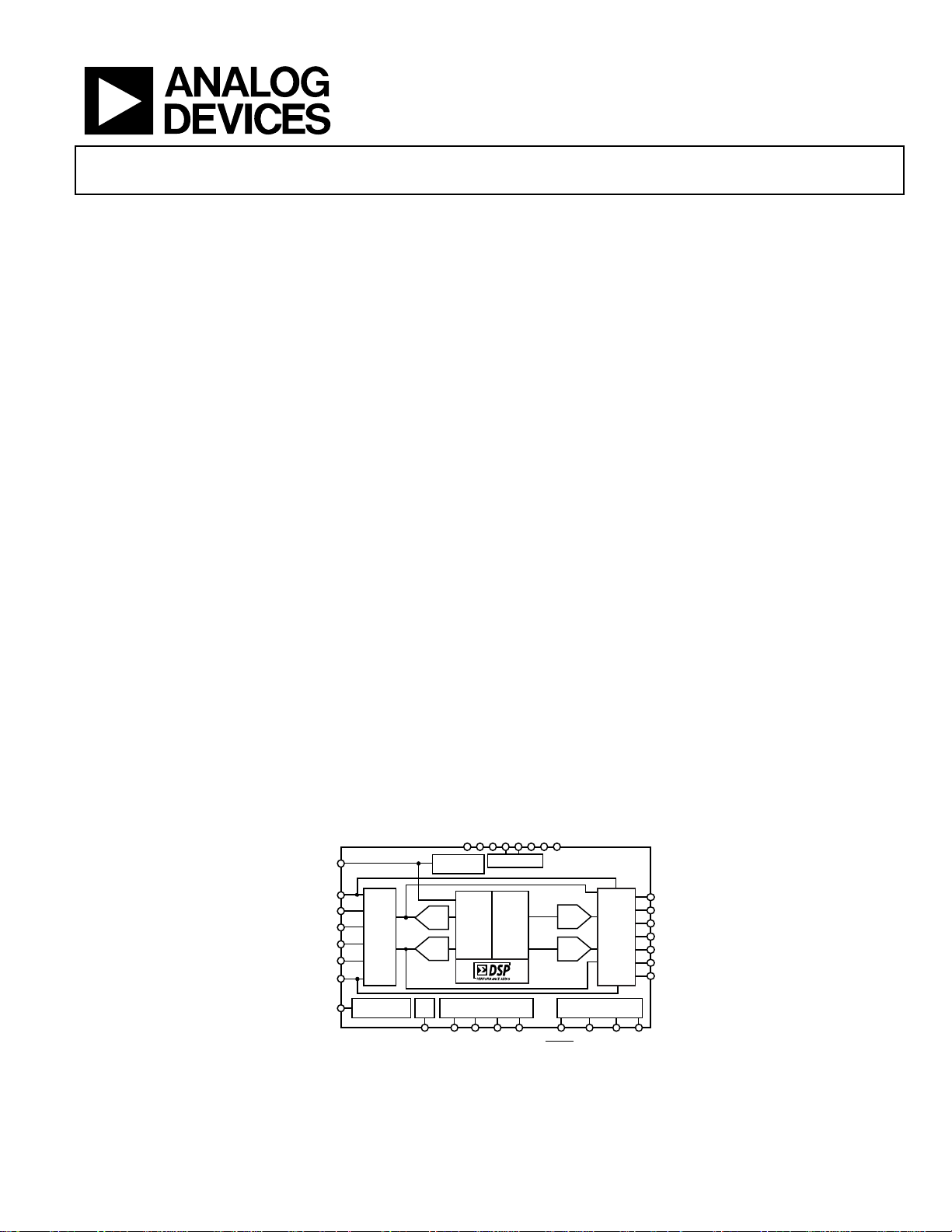
FUNCTIONAL BLOCK DIAGRAM
ADAU1761
GENERAL DESCRIPTION
The ADAU1761 is a low power, stereo audio codec with
integrated digital audio processing that supports stereo 48 kHz
record and playback at 14 mW from a 1.8 V analog supply. The
stereo audio ADCs and DACs support sample rates from 8 kHz
to 96 kHz as well as a digital volume control.
The SigmaDSP® core features 28-bit processing (56-bit double
precision). The processor allows system designers to compensate
for the real-world limitations of microphones, speakers, amplifiers,
and listening environments, resulting in a dramatic improvement
in the perceived audio quality through equalization, multiband
compression, limiting, and third-party branded algorithms.
The SigmaStudio™ graphical development tool is used to program
the ADAU1761. This software includes audio processing blocks
such as filters, dynamics processors, mixers, and low level DSP
functions for fast development of custom signal flows.
The record path includes an integrated microphone bias circuit
and six inputs. The inputs can be mixed and muxed before the
ADC, or they can be configured to bypass the ADC. The
ADAU1761 includes a stereo digital microphone input.
The ADAU1761 includes five high power output drivers (two
differential and three single-ended), supporting stereo headphones, an earpiece, or other output transducer. AC-coupled
or capless configurations are supported. Individual fine level
controls are supported on all analog outputs. The output mixer
stage allows for flexible routing of audio.
CM
IOVDD
DGND
ACKDET/MI CIN
LAUX
LINP
LINN
RINP
RINN
RAUX
MICBI AS
INPUT
MIXERS
ALC
MICRO PHONE
BIAS
HP JACK
DETECTIO N
ADC
PLL
INPUT/OUTPUT PORTS
MCLK
DC_SDATA/
REGULATOR
ADC
DIGI TAL
DIGI TAL
FILTERS
FILTERS
SERIAL DATA
GPIO1
BCLK/
GPIO2
LRCLK/
DVDDOUT
DAC
GPIO3
AGND
AVDD
AVDD
AGND
ADAU1761
LOUTP
SDA/
COUT
LOUTN
LHP
MONOOUT
RHP
ROUTP
ROUTN
07680-001
DAC
OUTPUT
MIXERS
DACADC
2
I
C/SPI
CONTROL PORT
SCL/
ADDR1/
ADDR0/
CLATCH
GPIO0
DAC_SDATA/
CDATA
CCLK
Figure 1.
Rev. C
Information furnished by Analog Devices is believed to be accurate and reliable. However, no
responsibility is assumed by Anal og Devices for its use, nor for any infringements of patents or ot her
rights of third parties that may result from its use. Specifications subject to change without notice. No
license is granted by implication or otherwise under any patent or patent rights of Analog Devices.
Trademarks and registered trademarks are the property of their respective owners.
One Technology Way, P.O. Box 9106, Norwood, MA 02062-9106, U.S.A.
Tel: 781.329.4700 www.analog.com
Fax: 781.461.3113 ©2009–2010 Analog Devices, Inc. All rights reserved.

ADAU1761
TABLE OF CONTENTS
Features.............................................................................................. 1
Applications....................................................................................... 1
General Description ......................................................................... 1
Functional Block Diagram .............................................................. 1
Revision History ............................................................................... 3
Specifications..................................................................................... 4
Analog Performance Specifications........................................... 4
Power Supply Specifications........................................................ 7
Typical Current Consumption.................................................... 8
Typical Power Management Measurements ............................. 9
Digital Filters............................................................................... 10
Digital Input/Output Specifications......................................... 10
Digital Timing Specifications ...................................................11
Digital Timing Diagrams........................................................... 12
Absolute Maximum Ratings.......................................................... 14
Thermal Resistance .................................................................... 14
ESD Caution................................................................................ 14
Pin Configuration and Function Descriptions........................... 15
Typical Performance Characteristics ........................................... 17
System Block Diagrams ................................................................. 20
Theory of Operation ...................................................................... 23
Startup, Initialization, and Power................................................. 24
Power-Up Sequence ................................................................... 24
Power Reduction Modes............................................................ 24
Digital Power Supply.................................................................. 24
Input/Output Power Supply...................................................... 24
Clock Generation and Management........................................ 24
Clocking and Sampling Rates .......................................................26
Core Clock................................................................................... 26
Sampling Rates............................................................................ 27
PLL ............................................................................................... 27
Record Signal Path.......................................................................... 29
Input Signal Paths....................................................................... 29
Analog-to-Digital Converters................................................... 31
Automatic Level Control (ALC)................................................... 32
ALC Parameters.......................................................................... 32
Noise Gate Function .................................................................. 33
Playback Signal Path ...................................................................... 35
Output Signal Paths ................................................................... 35
Headphone Output .................................................................... 36
Pop-and-Click Suppression ...................................................... 37
Line Outputs ............................................................................... 37
Control Ports................................................................................... 38
Burst Mode Writing and Reading............................................ 38
I2C Port ........................................................................................ 38
SPI Port........................................................................................ 41
Serial Data Input/Output Ports .................................................... 42
Applications Information.............................................................. 44
Power Supply Bypass Capacitors.............................................. 44
GSM Noise Filter........................................................................ 44
Grounding................................................................................... 44
Exposed Pad PCB Design ......................................................... 44
DSP Core ......................................................................................... 45
Signal Processing........................................................................ 45
Architecture ................................................................................ 45
Program Counter ....................................................................... 45
Features........................................................................................ 45
Startup.......................................................................................... 45
Numeric Formats ....................................................................... 46
Programming.............................................................................. 46
Program RAM, Parameter RAM, and Data RAM ..................... 47
Program RAM ............................................................................ 47
Parameter RAM.......................................................................... 47
Data RAM ................................................................................... 47
Read/Write Data Formats ......................................................... 47
Software Safeload ....................................................................... 48
Software Slew .............................................................................. 49
General-Purpose Input/Output.................................................... 50
GPIO Pins Set from the Control Port...................................... 50
Control Registers............................................................................ 51
Control Register Details ............................................................ 52
Outline Dimensions....................................................................... 92
Ordering Guide .......................................................................... 92
Rev. C | Page 2 of 92

ADAU1761
REVISION HISTORY
9/10—Rev. B to Rev. C
Changes to Figure 1...........................................................................1
5/10—Rev. A to Rev. B
Changes to Burst Mode Writing and Reading Section ..............38
Changes to Table 33 ........................................................................51
Added R67: Dejitter Control, 16,438 (0x4036) Section .............79
12/09—Rev. 0 to Rev. A
Changes to Features Section............................................................1
Change to General Description Section.........................................1
Changes to Table 1 ............................................................................6
Change to Table 5............................................................................10
Changes to Figure 6.........................................................................13
Changes to Table 10 ........................................................................15
Changes to Captions of Figure 15, Figure 16, Figure 18, and
Figure 19...........................................................................................18
Changes to Captions of Figure 21 and Figure 24........................19
Added Figure 25; Renumbered Sequentially...............................19
Change to Figure 26........................................................................20
Change to Figure 27........................................................................21
Change to Figure 28........................................................................22
Change to Theory of Operation Section......................................23
Changes to Power Reduction Modes Section and
Case 1: PLL Is Bypassed Section ...................................................24
Changes to PLL Lock Acquisition Section...................................25
Changes to Core Clock Section and Figure 30............................26
Change to Sampling Rates Section................................................27
Changes to Input Signal Paths Section and Figure 32................29
Changes to Figure 33 and Figure 34 .............................................30
Changes to ADC Full-Scale Level Section ...................................31
Change to Automatic Level Control (ALC) Section...................32
Changes to Output Signal Paths Section......................................35
Changes to Headphone Output Section.......................................36
Changes to Jack Detection Section, Pop-and-Click
Suppression Section, and Line Outputs Section .........................37
Changes to Control Ports Section and I
Added Burst Mode Writing and Reading Section ......................38
2
C Port Section ............38
Changes to SPI Port Section ..........................................................41
Changes to Serial Data Input/Output Ports Section
and Table 25.....................................................................................42
Added Figure 57..............................................................................42
Changes to Architecture Section and Figure 67..........................45
Added Startup Section....................................................................45
Changes to Parameter RAM Section and Data RAM Section ..47
Changes to Table 33........................................................................51
Changes to R2: Digital Microphone/Jack Detection Control,
16,392 (0x4008) Section and Table 36..........................................54
Changes to Table 42........................................................................58
Changes to Table 43........................................................................59
Changes to R15: Serial Port Control 0, 16,405 (0x4015)
Section and Table 49 ....................................................................... 63
Change to Table 50..........................................................................64
Changes to Table 51, R18: Converter Control 1, 16,408
(0x4018) Section, and Table 52 .....................................................65
Changes to Table 60, R27: Playback L/R Mixer Right (Mixer 6)
Line Output Control, 16,417 (0x4021) Section, and Table 61...71
Changes to Table 62, R29: Playback Headphone Left Volume
Control, 16,419 (0x4023) Section, and Table 63.........................72
Changes to Table 64........................................................................73
Changes to R42: Jack Detect Pin Control, 16,433 (0x4031)
Section and Table 76 ....................................................................... 79
Changes to R57: DSP Sampling Rate Setting, 16,619 (0x40EB)
Section and Table 81 ....................................................................... 81
Change to Table 85..........................................................................83
Change to Table 88..........................................................................84
Changes to R66: Clock Enable 1, 16,634 (0x40FA) Section
and Table 90.....................................................................................85
1/09—Revision 0: Initial Version
Rev. C | Page 3 of 92

ADAU1761
SPECIFICATIONS
Supply voltage (AVDD) = 3.3 V, TA = 25°C, master clock = 12.288 MHz (48 kHz fS, 256 × fS mode), input sample rate = 48 kHz, measurement
bandwidth = 20 Hz to 20 kHz, word width = 24 bits, C
(digital output) = 20 pF, I
LOAD
unless otherwise noted. Performance of all channels is identical, exclusive of the interchannel gain mismatch and interchannel phase
deviation specifications.
ANALOG PERFORMANCE SPECIFICATIONS
Specifications guaranteed at 25°C (ambient).
Table 1.
Parameter Test Conditions/Comments Min Typ Max Unit
ANALOG-TO-DIGITAL CONVERTERS
ADC Resolution All ADCs 24 Bits
Digital Attenuation Step 0.375 dB
Digital Attenuation Range 95 dB
INPUT RESISTANCE
Single-Ended Line Input −12 dB gain 83 kΩ
0 dB gain 21 kΩ
6 dB gain 10.5 kΩ
PGA Inverting Inputs −12 dB gain 84.5 kΩ
0 dB gain 53 kΩ
35.25 dB gain 2 kΩ
PGA Noninverting Inputs All gains 105 kΩ
SINGLE-ENDED LINE INPUT
Full-Scale Input Voltage (0 dB) Scales linearly with AVDD AVDD/3.3 V rms
AVDD = 1.8 V 0.55 (1.56) V rms (V p-p)
AVDD = 3.3 V 1.0 (2.83) V rms (V p-p)
Dynamic Range 20 Hz to 20 kHz, −60 dB input
With A-Weighted Filter (RMS) AVDD = 1.8 V 94 dB
AVDD = 3.3 V 99 dB
No Filter (RMS) AVDD = 1.8 V 91 dB
AVDD = 3.3 V 96 dB
Total Harmonic Distortion + Noise −1 dBFS
AVDD = 1.8 V −88 dB
AVDD = 3.3 V −90 dB
Signal-to-Noise Ratio
With A-Weighted Filter (RMS) AVDD = 1.8 V 94 dB
AVDD = 3.3 V 99 dB
No Filter (RMS) AVDD = 1.8 V 91 dB
AVDD = 3.3 V 96 dB
Gain per Step 3 dB
Total Gain Range −12 +6 dB
Mute Attenuation −87 dB
Interchannel Gain Mismatch 0.005 dB
Offset Error 0 mV
Gain Error −12 %
Interchannel Isolation 68 dB
Power Supply Rejection Ratio CM capacitor = 20 F
100 mV p-p @ 217 Hz 65 dB
100 mV p-p @ 1 kHz 67 dB
ADC performance excludes mixers
and PGA
(digital output) = 2 mA, VIH = 2 V, VIL = 0.8 V,
LOAD
Rev. C | Page 4 of 92

ADAU1761
Parameter Test Conditions/Comments Min Typ Max Unit
PSEUDO-DIFFERENTIAL PGA INPUT
Full-Scale Input Voltage (0 dB) Scales linearly with AVDD AVDD/3.3 V rms
AVDD = 1.8 V 0.55 (1.56) V rms (V p-p)
AVDD = 3.3 V 1.0 (2.83) V rms (V p-p)
Dynamic Range 20 Hz to 20 kHz, −60 dB input
With A-Weighted Filter (RMS) AVDD = 1.8 V 92 dB
AVDD = 3.3 V 98 dB
No Filter (RMS) AVDD = 1.8 V 90 dB
AVDD = 3.3 V 95 dB
Total Harmonic Distortion + Noise −1 dBFS
AVDD = 1.8 V −88 dB
AVDD = 3.3 V −89 dB
Signal-to-Noise Ratio
With A-Weighted Filter (RMS) AVDD = 1.8 V 92 dB
AVDD = 3.3 V 98 dB
No Filter (RMS) AVDD = 1.8 V 90 dB
AVDD = 3.3 V 95 dB
Volume Control Step PGA gain 0.75 dB
Volume Control Range PGA gain −12 +35.25 dB
PGA Boost 20 dB
Mute Attenuation −87 dB
Interchannel Gain Mismatch 0.005 dB
Offset Error 0 mV
Gain Error −14 %
Interchannel Isolation 83 dB
Common-Mode Rejection Ratio 100 mV rms, 1 kHz 65 dB
100 mV rms, 20 kHz 65 dB
FULL DIFFERENTIAL PGA INPUT Differential PGA inputs
Full-Scale Input Voltage (0 dB) Scales linearly with AVDD AVDD/3.3 V rms
AVDD = 1.8 V 0.55 (1.56) V rms (V p-p)
AVDD = 3.3 V 1.0 (2.83) V rms (V p-p)
Dynamic Range 20 Hz to 20 kHz, −60 dB input
With A-Weighted Filter (RMS) AVDD = 1.8 V 92 dB
AVDD = 3.3 V 98 dB
No Filter (RMS) AVDD = 1.8 V 90 dB
AVDD = 3.3 V 95 dB
Total Harmonic Distortion + Noise −1 dBFS
AVDD = 1.8 V −70 dB
AVDD = 3.3 V −78 dB
Signal-to-Noise Ratio
With A-Weighted Filter (RMS) AVDD = 1.8 V 92 dB
AVDD = 3.3 V 98 dB
No Filter (RMS) AVDD = 1.8 V 90 dB
AVDD = 3.3 V 95 dB
Volume Control Step PGA gain 0.75 dB
Volume Control Range PGA gain −12 +35.25 dB
PGA Boost 20 dB
Mute Attenuation −87 dB
Interchannel Gain Mismatch 0.005 dB
Offset Error 0 mV
Gain Error −14 %
Rev. C | Page 5 of 92

ADAU1761
Parameter Test Conditions/Comments Min Typ Max Unit
Interchannel Isolation 83 dB
Common-Mode Rejection Ratio 100 mV rms, 1 kHz 65 dB
100 mV rms, 20 kHz 65 dB
MICROPHONE BIAS MBIEN = 1
Bias Voltage
0.65 × AVDD AVDD = 1.8 V, MBI = 1 1.17 V
AVDD = 3.3 V, MBI = 1 2.145 V
0.90 × AVDD AVDD = 1.8 V, MBI = 0 1.62 V
AVDD = 3.3 V, MBI = 0 2.97 V
Bias Current Source AVDD = 3.3 V, MBI = 0, MPERF = 1 3 mA
Noise in the Signal Bandwidth AVDD = 3.3 V, 1 kHz to 20 kHz
MBI = 0, MPERF = 0 42 nV/√Hz
MBI = 0, MPERF = 1 85 nV/√Hz
MBI = 1, MPERF = 0 25 nV/√Hz
MBI = 1, MPERF = 1 37 nV/√Hz
DIGITAL-TO-ANALOG CONVERTERS
DAC Resolution All DACs 24 Bits
Digital Attenuation Step 0.375 dB
Digital Attenuation Range 95 dB
DAC TO LINE OUTPUT
Full-Scale Output Voltage (0 dB) Scales linearly with AVDD AVDD/3.3 V rms
AVDD = 1.8 V 0.50 (1.41) V rms (V p-p)
AVDD = 3.3 V 0.92 (2.60) V rms (V p-p)
Analog Volume Control Step Line output volume control 0.75 dB
Analog Volume Control Range Line output volume control −57 1 +6 dB
Mute Attenuation −87 dB
Dynamic Range
With A-Weighted Filter (RMS) AVDD = 1.8 V 96 dB
AVDD = 3.3 V 101 dB
No Filter (RMS) AVDD = 1.8 V 93.5 dB
AVDD = 3.3 V 98 dB
Total Harmonic Distortion + Noise −1 dBFS, line output mode dB
AVDD = 1.8 V −90 dB
AVDD = 3.3 V −92 dB
Signal-to-Noise Ratio Line output mode
With A-Weighted Filter (RMS) AVDD = 1.8 V 96 dB
AVDD = 3.3 V 101 dB
No Filter (RMS) AVDD = 1.8 V 93.5 dB
AVDD = 3.3 V 98 dB
Power Supply Rejection Ratio CM capacitor = 20 F
100 mV p-p @ 217 Hz 56 dB
100 mV p-p @ 1 kHz 70 dB
Gain Error 3 %
Interchannel Gain Mismatch 0.005 dB
Offset Error 0 mV
Interchannel Isolation 1 kHz, 0 dBFS input signal 100 dB
DAC performance excludes mixers and
headphone amplifier
20 Hz to 20 kHz, −60 dB input, line
output mode
Rev. C | Page 6 of 92
ADAU1761
Parameter Test Conditions/Comments Min Typ Max Unit
= output power per channel
DAC TO HEADPHONE/EARPIECE
OUTPUT
Full-Scale Output Voltage (0 dB) Scales linearly with AVDD AVDD/3.3 V rms
AVDD = 1.8 V 0.50 (1.41) V rms (V p-p)
AVDD = 3.3 V 0.92 (2.60) V rms (V p-p)
Total Harmonic Distortion + Noise −4 dBFS
16 Ω load AVDD = 1.8 V, PO = 6.4 mW −76 dB
AVDD = 3.3 V, PO = 21.1 mW −82 dB
32 Ω load AVDD = 1.8 V, PO = 3.8 mW −82 dB
AVDD = 3.3 V, PO = 10.6 mW −82 dB
Power Supply Rejection Ratio CM capacitor = 20 F
100 mV p-p @ 217 Hz 56 dB
100 mV p-p @ 1 kHz 67 dB
Interchannel Isolation
Referred to GND 73 dB
REFERENCE
Common-Mode Reference Output CM pin AVDD/2 V
P
O
1 kHz, 0 dBFS input signal, 32 Ω load,
AVDD = 3.3 V
Referred to CM (capless headphone
mode)
50 dB
POWER SUPPLY SPECIFICATIONS
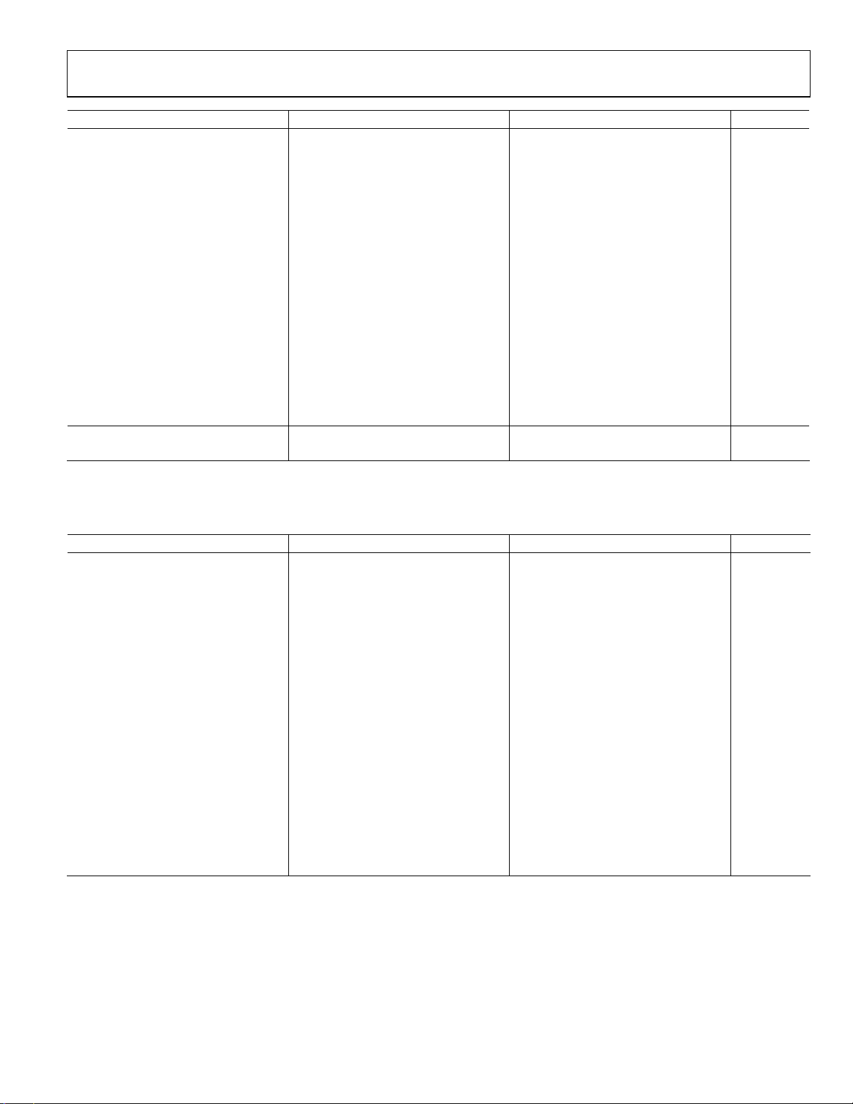
Table 2.
Parameter Test Conditions/Comments Min Typ Max Unit
SUPPLIES
Voltage DVDDOUT 1.56 V
AVDD 1.8 3.3 3.65 V
IOVDD 1.63 3.3 3.65 V
Digital I/O Current (IOVDD = 1.8 V) 20 pF capacitive load on all digital pins
Slave Mode fS = 48 kHz 0.25 mA
f
f
Master Mode fS = 48 kHz 0.62 mA
f
f
Digital I/O Current (IOVDD = 3.3 V) 20 pF capacitive load on all digital pins
Slave Mode fS = 48 kHz 0.48 mA
f
f
Master Mode fS = 48 kHz 1.51 mA
f
f
Analog Current (AVDD) See Table 3
= 96 kHz 0.48 mA
S
= 8 kHz 0.07 mA
S
= 96 kHz 1.23 mA
S
= 8 kHz 0.11 mA
S
= 96 kHz 0.9 mA
S
= 8 kHz 0.13 mA
S
= 96 kHz 3 mA
S
= 8 kHz 0.27 mA
S
Rev. C | Page 7 of 92
ADAU1761
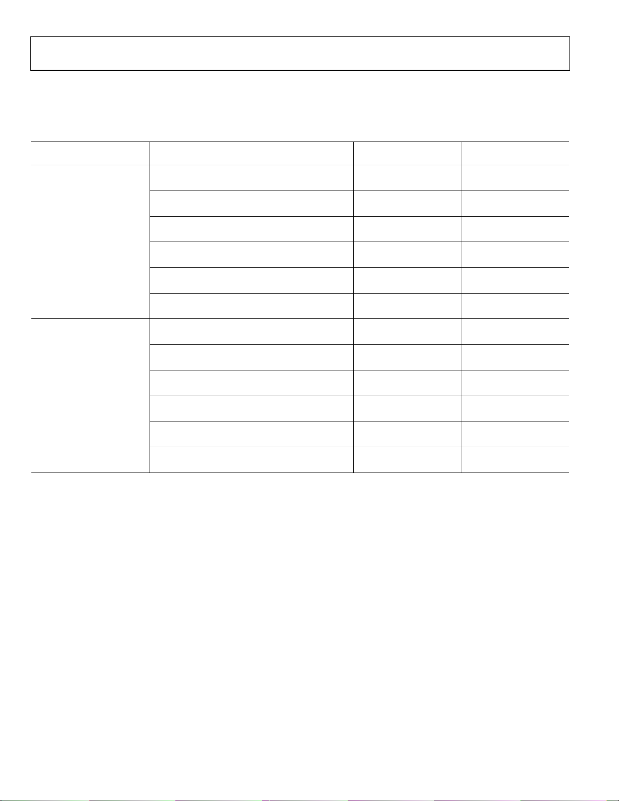
TYPICAL CURRENT CONSUMPTION
Master clock = 12.288 MHz, input sample rate = 48 kHz, input tone = 1 kHz, normal power management settings, ADC input @ −1 dBFS,
DAC input @ 0 dBFS. For total power consumption, add the IOVDD current listed in Tab le 2 .
Table 3.
Typical AVDD Current
Operating Voltage Audio Path Clock Generation
AVDD = IOVDD = 3.3 V
DAC stereo playback to line output (10 kΩ)
AVDD = IOVDD = 1.8 V
DAC stereo playback to line output (10 kΩ)
Direct MCLK 5.24 Record stereo differential to ADC
Integer PLL 6.57
Direct MCLK 5.55
Integer PLL 6.90
Direct MCLK 55.5 DAC stereo playback to headphone (16 Ω)
Integer PLL 56.8
Direct MCLK 30.9 DAC stereo playback to headphone (32 Ω)
Integer PLL 32.25
Direct MCLK 56.75 DAC stereo playback to capless headphone (32 Ω)
Integer PLL 58
Direct MCLK 1.9 Record aux stereo bypass to line output (10 kΩ)
Integer PLL 3.3
Direct MCLK 4.25 Record stereo differential to ADC
Integer PLL 5.55
Direct MCLK 4.7
Integer PLL 5.7
Direct MCLK 30.81 DAC stereo playback to headphone (16 Ω)
Integer PLL 32
Direct MCLK 18.3 DAC stereo playback to headphone (32 Ω)
Integer PLL 19.5
Direct MCLK 32.6 DAC stereo playback to capless headphone (32 Ω)
Integer PLL 33.7
Direct MCLK 1.9 Record aux stereo bypass to line output (10 kΩ)
Integer PLL 3.07
Consumption (mA)
Rev. C | Page 8 of 92

ADAU1761
TYPICAL POWER MANAGEMENT MEASUREMENTS
Master clock = 12.288 MHz, integer PLL, input sample rate = 48 kHz, input tone = 1 kHz. Pseudo-differential input to ADCs, DACs to
line output with 10 k load. ADC input @ −1 dBFS, DAC input @ 0 dBFS. In Tab l e 4 , the mixer boost and power management conditions
are set for MXBIAS[1:0], ADCBIAS[1:0], HPBIAS[1:0], and DACBIAS[1:0]. RBIAS[1:0] and PBIAS[1:0] do not have an extreme power
saving mode and are therefore set for power saving mode in the extreme power saving rows in Tab l e 4 .
Table 4.
Typical
Operating Voltage
AVDD = IOVDD = 3.3 V
AVDD = IOVDD = 1.8 V
Power Management
Setting
Mixer Boost
Setting
Normal operation 9.6 −91 −92.5 Normal (default)
Boost Level 1 9.75 −91.5 −92.5
Boost Level 2 9.92 −91.5 −92.5
Boost Level 3 10.25 −91.5 −92.5
Normal operation 7.09 −84.5 −87 Extreme power saving
Boost Level 1 7.19 −84.8 −87.1
Boost Level 2 7.29 −84.8 −87.1
Boost Level 3 7.49 −85 −87.1
Normal operation 7.67 −89.5 −90 Power saving
Boost Level 1 7.77 −89.5 −90
Boost Level 2 7.86 −89.8 −90
Boost Level 3 8.07 −89.8 −90
Normal operation 10.55 −91 −93.5 Enhanced performance
Boost Level 1 10.74 −91 −93.5
Boost Level 2 10.93 −91 −93.5
Boost Level 3 11.33 −91 −93.5
Normal operation 8.1 −88 −91.2 Normal (default)
Boost Level 1 8.26 −88 −91.2
Boost Level 2 8.41 −88 −91.2
Boost Level 3 8.73 −88 −91.2
Normal operation 5.73 −85 −86 Extreme power saving
Boost Level 1 5.82 −85.4 −86
Boost Level 2 5.91 −85.5 −86
Boost Level 3 6.1 −85.5 −86
Normal operation 6.27 −86 −89.4 Power saving
Boost Level 1 6.36 −86.1 −89.5
Boost Level 2 6.46 −86.3 −89.5
Boost Level 3 6.65 −86.3 −89.5
Normal operation 9.01 −88 −91.5 Enhanced performance
Boost Level 1 9.2 −88 −91.5
Boost Level 2 9.38 −88 −91.5
Boost Level 3 9.76 −88 −91.5
AVD D Curre nt
Consumption (mA)
Typical ADC
THD + N (dB)
Typical Line Output
THD + N (dB)
Rev. C | Page 9 of 92

ADAU1761
DIGITAL FILTERS
Table 5.
Parameter Mode Factor Min Typ Max Unit
ADC DECIMATION FILTER All modes, typ @ 48 kHz
Pass Band 0.4375 fS 21 kHz
Pass-Band Ripple ±0.015 dB
Transition Band 0.5 fS 24 kHz
Stop Band 0.5625 fS 27 kHz
Stop-Band Attenuation 67 dB
Group Delay 22.9844/fS 479 µs
DAC INTERPOLATION FILTER
Pass Band 48 kHz mode, typ @ 48 kHz 0.4535 fS 22 kHz
96 kHz mode, typ @ 96 kHz 0.3646 fS 35 kHz
Pass-Band Ripple 48 kHz mode, typ @ 48 kHz ±0.01 dB
96 kHz mode, typ @ 96 kHz ±0.05 dB
Transition Band 48 kHz mode, typ @ 48 kHz 0.5 fS 24 kHz
96 kHz mode, typ @ 96 kHz 0.5 fS 48 kHz
Stop Band 48 kHz mode, typ @ 48 kHz 0.5465 fS 26 kHz
96 kHz mode, typ @ 96 kHz 0.6354 fS 61 kHz
Stop-Band Attenuation 48 kHz mode, typ @ 48 kHz 69 dB
96 kHz mode, typ @ 96 kHz 68 dB
Group Delay 48 kHz mode, typ @ 48 kHz 25/fS 521 µs
96 kHz mode, typ @ 96 kHz 11/fS 115 µs
DIGITAL INPUT/OUTPUT SPECIFICATIONS
−40°C < TA < +85°C, IOVDD = 3.3 V ± 10%.
Table 6.
Parameter Test Conditions/Comments Min Typ Max Unit
INPUT SPECIFICATIONS
Input Voltage High (VIH) 0.7 × IOVDD V
Input Voltage Low (VIL) 0.3 × IOVDD V
Input Leakage
Pull-Ups/Pull-Downs Disabled IIH @ VIH = 3.3 V −0.17 +0.17 µA
I
I
Pull-Ups Enabled IIH @ VIH = 3.3 V −0.7 +0.7 µA
I
Pull-Downs Enabled IIH @ VIH = 3.3 V 2.7 8.3 µA
I
Input Capacitance 5 pF
OUTPUT SPECIFICATIONS
Output Voltage High (VOH) IOH = 2 mA @ 3.3 V, 0.85 mA @ 1.8 V 0.8 × IOVDD V
Output Voltage Low (VOL) IOL = 2 mA @ 3.3 V, 0.85 mA @ 1.8 V 0.1 × IOVDD V
@ VIL = 0 V −0.17 +0.17 µA
IL
@ VIL = 0 V (MCLK pin) −13.5 −0.5 µA
IL
@ VIL = 0 V −13.5 −0.5 µA
IL
@ VIL = 0 V −0.18 +0.18 µA
IL
Rev. C | Page 10 of 92
ADAU1761
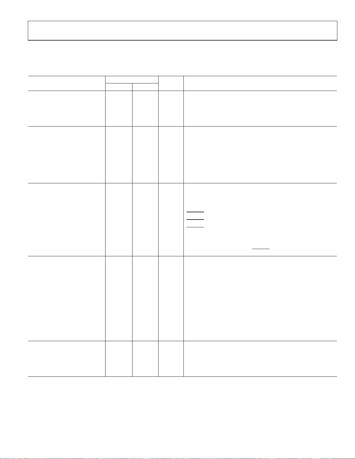
DIGITAL TIMING SPECIFICATIONS
−40°C < TA < +85°C, IOVDD = 3.3 V ± 10%.
Table 7. Digital Timing
Limit
Parameter
t
t
MIN
MAX
MASTER CLOCK
tMP 74 488 ns MCLK period, 256 × fS mode.
tMP 37 244 ns MCLK period, 512 × fS mode.
tMP 24.7 162.7 ns MCLK period, 768 × fS mode.
tMP 18.5 122 ns MCLK period, 1024 × fS mode.
SERIAL PORT
t
5 ns BCLK pulse width low.
BIL
t
5 ns BCLK pulse width high.
BIH
t
5 ns LRCLK setup. Time to BCLK rising.
LIS
t
5 ns LRCLK hold. Time from BCLK rising.
LIH
t
5 ns DAC_SDATA setup. Time to BCLK rising.
SIS
t
5 ns DAC_SDATA hold. Time from BCLK rising.
SIH
t
50 ns ADC_SDATA delay. Time from BCLK falling in master mode.
SODM
SPI PORT
f
10 MHz CCLK frequency.
CCLK
t
10 ns CCLK pulse width low.
CCPL
t
10 ns CCLK pulse width high.
CCPH
t
5 ns
CLS
t
10 ns
CLH
t
10 ns
CLPH
t
5 ns CDATA setup. Time to CCLK rising.
CDS
t
5 ns CDATA hold. Time from CCLK rising.
CDH
t
50 ns
COD
I2C PORT
f
400 kHz SCL frequency.
SCL
t
0.6 µs SCL high.
SCLH
t
1.3 µs SCL low.
SCLL
t
0.6 µs Setup time; relevant for repeated start condition.
SCS
t
0.6 µs Hold time. After this period, the first clock is generated.
SCH
tDS 100 ns Data setup time.
t
300 ns SCL rise time.
SCR
t
300 ns SCL fall time.
SCF
t
300 ns SDA rise time.
SDR
t
300 ns SDA fall time.
SDF
t
0.6 µs Bus-free time. Time between stop and start.
BFT
DIGITAL MICROPHONE R
t
10 ns Digital microphone clock fall time.
DCF
t
10 ns Digital microphone clock rise time.
DCR
t
22 30 ns Digital microphone delay time for valid data.
DDV
t
0 12 ns Digital microphone delay time for data three-stated.
DDH
Unit Description
setup. Time to CCLK rising.
CLATCH
hold. Time from CCLK rising.
CLATCH
pulse width high.
CLATCH
COUT three-stated. Time from CLATCH
= 1 MΩ, C
LOAD
LOAD
rising.
= 14 pF.
Rev. C | Page 11 of 92

ADAU1761
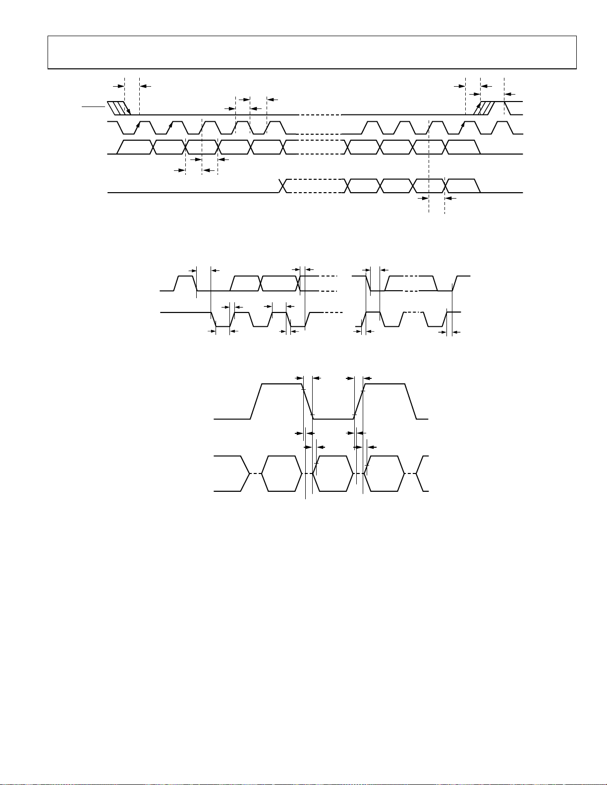
DIGITAL TIMING DIAGRAMS
t
LIH
t
SIS
LSB
t
SIH
07680-002
RIGHT-JUSTIFIED
BCLK
LRCLK
DAC_SDATA
LEFT-JUSTIFIED
MODE
DAC_SDATA
2
I
S MODE
DAC_SDATA
MODE
BCLK
t
BIH
t
BIL
t
LIS
t
SIS
MSB
t
SIH
8-BIT CLOCKS
(24-BIT DATA)
12-BIT CLOCKS
(20-BIT DATA)
14-BIT CLOCKS
(18-BIT DATA)
16-BIT CLOCKS
(16-BIT DATA)
t
SIS
MSB – 1
MSB
t
SIH
t
SIS
MSB
t
SIH
Figure 2. Serial Input Port Timing
t
BIH
t
BIL
LRCLK
ADC_SDATA
LEFT-JUSTIFIED
RIGHT -JUSTI FIE D
MODE
ADC_SDATA
2
I
S MODE
ADC_SDATA
MODE
t
SODM
MSB
8-BIT CLOCKS
(24-BIT DATA)
12-BIT CLO CKS
(20-BIT DATA)
14-BIT CLO CKS
(18-BIT DATA)
16-BIT CLO CKS
(16-BIT DATA)
t
SODM
MSB – 1
MSB
Figure 3. Serial Output Port Timing
Rev. C | Page 12 of 92
t
SODM
MSB
LSB
07680-003
ADAU1761
t
CLS
t
CCPL
CLATCH
CCLK
CDATA
COUT
t
CCPH
t
t
CDS
CDH
Figure 4. SPI Port Timing
t
t
SCLH
DS
t
SCH
SDA
t
SCH
t
SCR
t
CLH
t
COD
t
CLPH
07680-004
SCL
t
SCLL
t
SCF
Figure 5. I
2
C Port Timing
t
SCS
t
BFT
07680-005
t
CLK
DATA1/
DATA1 DATA1 DATA2DATA2
DATA2
t
DCF
DDH
t
DDV
t
DDH
t
DCR
t
DDV
07680-006
Figure 6. Digital Microphone Timing
Rev. C | Page 13 of 92

ADAU1761
ABSOLUTE MAXIMUM RATINGS
Table 8.
Parameter Rating
Power Supply (AVDD) −0.3 V to +3.65 V
Input Current (Except Supply Pins) ±20 mA
Analog Input Voltage (Signal Pins) −0.3 V to AVDD + 0.3 V
Digital Input Voltage (Signal Pins) −0.3 V to IOVDD + 0.3 V
Operating Temperature Range −40°C to +85°C
Storage Temperature Range −65°C to +150°C
Stresses above those listed under Absolute Maximum Ratings
may cause permanent damage to the device. This is a stress
rating only; functional operation of the device at these or any
other conditions above those indicated in the operational
section of this specification is not implied. Exposure to absolute
maximum rating conditions for extended periods may affect
device reliability.
THERMAL RESISTANCE
θJA represents thermal resistance, junction-to-ambient; θJC represents thermal resistance, junction-to-case. All characteristics are
for a 4-layer board.
Table 9. Thermal Resistance
Package Type θJA θ
32-Lead LFCSP 50.1 17 °C/W
Unit
JC
ESD CAUTION
Rev. C | Page 14 of 92

ADAU1761
PIN CONFIGURATION AND FUNCTION DESCRIPTIONS
SCL/CCLK
SDA/COUT
ADDR1/CDATA
LRCLK/GPI O3
BCLK/GPIO 2
DAC_SDATA/GPI O0
ADC_SDATA/GPI O1
DGND
28
27
26
25
29
31
30
32
14
15
RAUX
ROUTP
24 DVDDOUT
23 AVDD
22 AGND
21 MONOOUT
20 LHP
19 RHP
18 LOUTP
17 LOUTN
16
ROUTN
07680-007
1IOVDD
PIN 1
2MCLK
INDICATOR
3ADDR0/CLATCH
4JACKDET/MICI N
ADAU1761
5MICBIAS
6LAUX
7CM
8AVDD
NOTES
1. THE EXPOSED PAD IS CONNECTED INT ERNALLY TO THE
ADAU1761 GROUNDS. FOR INCREASED REL IABILITY OF T HE
SOLDER JOINTS AND MAXIMUM THERMAL CAPABILITY, IT IS
RECOMMENDED THAT THE PAD BE SOLDERED TO THE
GROUND PLANE.
TOP VIEW
(Not to Scale)
9
11
12
10
LINP
LINN
RINP
AGND
13
RINN
Figure 7. Pin Configuration
Table 10. Pin Function Descriptions
Pin No. Mnemonic Type1 Description
1 IOVDD PWR
Supply for Digital Input and Output Pins. The digital output pins are supplied from IOVDD,
which also sets the highest input voltage that should be seen on the digital input pins.
IOVDD should be set between 1.8 V and 3.3 V. The current draw of this pin is variable because
it is dependent on the loads of the digital outputs. IOVDD should be decoupled to DGND
with a 100 nF capacitor and a 10 F capacitor.
2 MCLK D_IN External Master Clock Input.
3
ADDR0/CLATCH
D_IN I
2
C Address Bit 0 (ADDR0).
SPI Latch Signal (CLATCH
). Must go low at the beginning of an SPI transaction and high at the
end of a transaction. Each SPI transaction can take a different number of CCLKs to complete,
depending on the address and read/write bit that are sent at the beginning of the SPI
transaction.
4 JACKDET/MICIN D_IN Detect Insertion/Removal of Headphone Plug (JACKDET).
Digital Microphone Stereo Input (MICIN).
5 MICBIAS A_OUT Bias Voltage for Electret Microphone.
6 LAUX A_IN Left Channel Single-Ended Auxiliary Input. Biased at AVDD/2.
7 CM A_OUT
AVDD/2 V Common-Mode Reference. A 10 F to 47 F standard decoupling capacitor should
be connected between this pin and AGND to reduce crosstalk between the ADCs and DACs.
This pin can be used to bias external analog circuits, as long as they are not drawing current
from CM (for example, the noninverting input of an op amp).
8 AVDD PWR
1.8 V to 3.65 V Analog Supply for DAC and Microphone Bias. This pin should be decoupled
locally to AGND with a 100 nF capacitor.
9 AGND PWR
Analog Ground. The AGND and DGND pins can be tied together on a common ground plane.
AGND should be decoupled locally to AVDD with a 100 nF capacitor.
10 LINP A_IN Left Channel Noninverting Input or Single-Ended Input 0. Biased at AVDD/2.
11 LINN A_IN Left Channel Inverting Input or Single-Ended Input 1. Biased at AVDD/2.
12 RINP A_IN Right Channel Noninverting Input or Single-Ended Input 2. Biased at AVDD/2.
13 RINN A_IN Right Channel Inverting Input or Single-Ended Input 3. Biased at AVDD/2.
14 RAUX A_IN Right Channel Single-Ended Auxiliary Input. Biased at AVDD/2.
15 ROUTP A_OUT Right Line Output, Positive. Biased at AVDD/2.
16 ROUTN A_OUT Right Line Output, Negative. Biased at AVDD/2.
17 LOUTN A_OUT Left Line Output, Negative. Biased at AVDD/2.
18 LOUTP A_OUT Left Line Output, Positive. Biased at AVDD/2.
Rev. C | Page 15 of 92

ADAU1761
Pin No. Mnemonic Type1 Description
19 RHP A_OUT Right Headphone Output. Biased at AVDD/2.
20 LHP A_OUT Left Headphone Output. Biased at AVDD/2.
21 MONOOUT A_OUT
22 AGND PWR
23 AVDD PWR
24 DVDDOUT PWR
25 DGND PWR
26 ADC_SDATA/GPIO1 D_IO ADC Serial Output Data (ADC_SDATA).
27 DAC_SDATA/GPIO0 D_IO DAC Serial Input Data (DAC_SDATA).
28 BCLK/GPIO2 D_IO Serial Data Port Bit Clock (BCLK).
29 LRCLK/GPIO3 D_IO Serial Data Port Frame Clock (LRCLK).
30 ADDR1/CDATA D_IN I2C Address Bit 1 (ADDR1).
31 SDA/COUT D_IO
32 SCL/CCLK D_IN
EP Exposed Pad
1
A_IN = analog input, A_OUT = analog output, D_IN = digital input, D_IO = digital input/output, PWR = power.
Mono Output or Virtual Ground for Capless Headphone. Biased at AVDD/2 when set as mono
output.
Analog Ground. The AGND and DGND pins can be tied together on a common ground plane.
AGND should be decoupled locally to AVDD with a 100 nF capacitor.
1.8 V to 3.3 V Analog Supply for ADC, Output Driver, and Input to Digital Supply Regulator.
This pin should be decoupled locally to AGND with a 100 nF capacitor.
Digital Core Supply Decoupling Point. The digital supply is generated from an on-board
regulator and does not require an external supply. DVDDOUT should be decoupled to DGND
with a 100 nF capacitor and a 10 F capacitor.
Digital Ground. The AGND and DGND pins can be tied together on a common ground plane.
DGND should be decoupled to DVDDOUT and to IOVDD with 100 nF capacitors and 10 F
capacitors.
General-Purpose Input/Output 1 (GPIO1).
General-Purpose Input/Output 0 (GPIO0).
General-Purpose Input/Output 2 (GPIO2).
General-Purpose Input/Output 3 (GPIO3).
SPI Data Input (CDATA).
2
C Data (SDA). This pin is a bidirectional open-collector input/output. The line connected to
I
this pin should have a 2 kΩ pull-up resistor.
SPI Data Output (COUT). This pin is used for reading back registers and memory locations. It is
three-state when an SPI read is not active.
2
C Clock (SCL). This pin is always an open-collector input when in I2C control mode. The line
I
connected to this pin should have a 2 kΩ pull-up resistor.
SPI Clock (CCLK). This pin can run continuously or be gated off between SPI transactions.
Exposed Pad. The exposed pad is connected internally to the ADAU1761 grounds. For
increased reliability of the solder joints and maximum thermal capability, it is recommended
that the pad be soldered to the ground plane. See the Exposed Pad PCB Design section for
more information.
Rev. C | Page 16 of 92
ADAU1761
–
TYPICAL PERFORMANCE CHARACTERISTICS
28
26
24
22
20
18
16
14
12
10
8
6
STEREO OUTPUT PO WER (mW)
4
2
0
–60 0–10–20–30–40–50
DIGITAL 1kHz INPUT SIGNAL (dBFS)
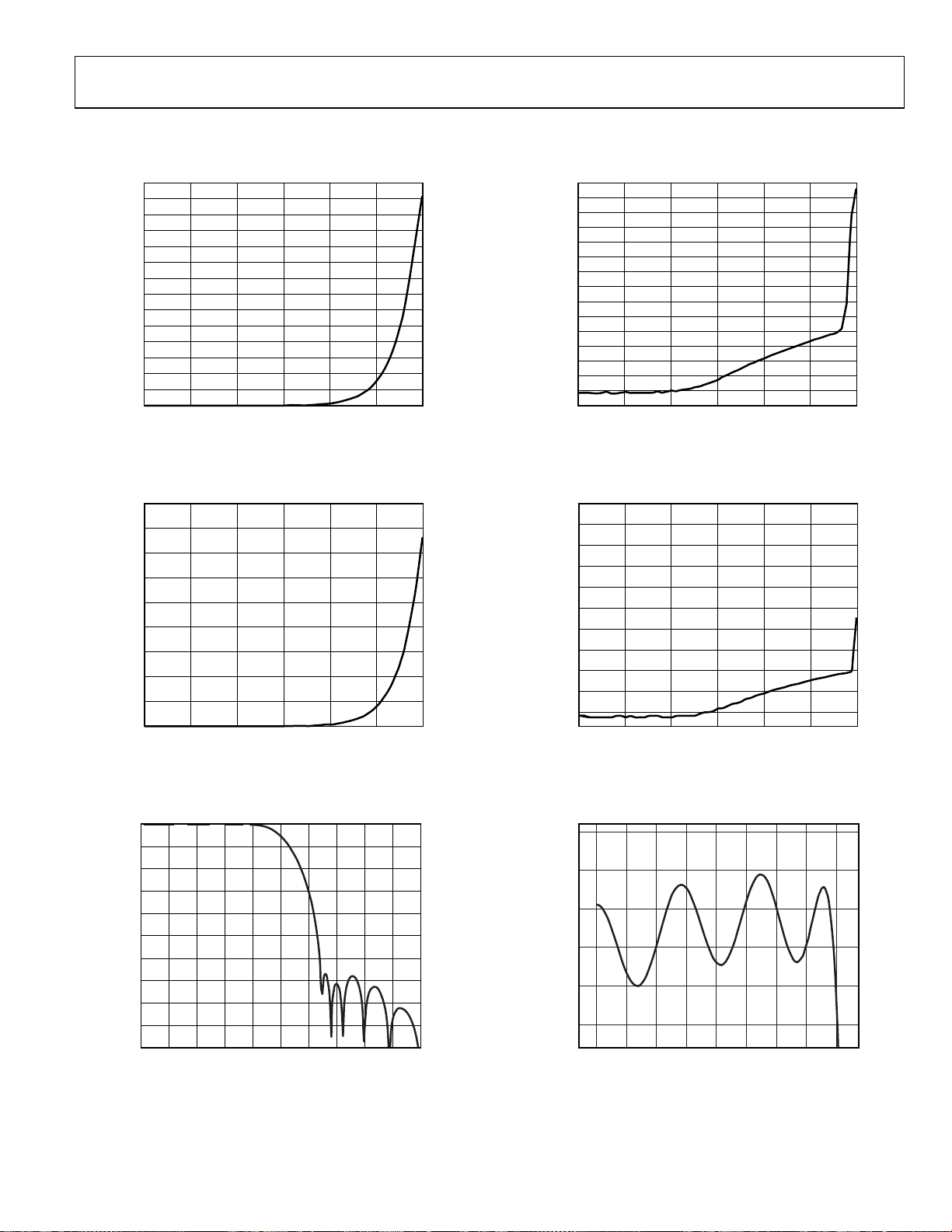
Figure 8. Headphone Amplifier Power vs. Input Level, 16 Ω Load
07680-055
30
–35
–40
–45
–50
–55
–60
–65
–70
–75
THD + N (dBV)
–80
–85
–90
–95
–100
–105
–60 0–10–20–30–40–50
DIGITAL 1kHz INPUT SIGNAL (dBFS)
Figure 11. Headphone Amplifier THD + N vs. Input Level, 16 Ω Load
07680-056
18
16
14
12
10
8
6
4
STEREO OUTPUT PO WER (mW)
2
0
–60 0–10–20–30–40–50
DIGITAL 1kHz INPUT SIGNAL (dBFS)
Figure 9. Headphone Amplifier Power vs. Input Level, 32 Ω Load
0
10
20
30
40
50
60
MAGNITUDE (d BFS)
70
80
90
100
0 0.1 0.2 0.3 0.4 0.5 0.6 0.7 0.8 0.9 1.0
FREQUENCY (NORMALIZED T O
f
)
S
Figure 10. ADC Decimation Filter, 64× Oversampling, Normalized to f
0
–10
–20
–30
–40
–50
–60
THD + N (dBV)
–70
–80
–90
–100
–60 0–10–20–30–40–50
07680-057
DIGITAL 1kHz INPUT SI GNAL (dBF S)
07680-058
Figure 12. Headphone Amplifier THD + N vs. Input Level, 32 Ω Load
0.04
0.02
0
–0.02
MAGNITUDE (dBFS)
–0.04
–0.06
0 0.05 0.10 0.20 0.30 0.400.15 0.25 0.35
07680-008
S
Figure 13. ADC Decimation Filter Pass-Band Ripple, 64× Oversampling,
FREQUENCY (NORMALIZED TO
Normalized to f
f
)
S
S
07680-009
Rev. C | Page 17 of 92
ADAU1761
0
–10
–20
–30
–40
–50
–60
MAGNITUDE (d BFS)
–70
–80
–90
–100
0.10 0. 2 0.3 0.4 0.5 0.6 0.7 0.8 0.9 1.0
FREQUENCY (NORMALIZED TO
f
)
S
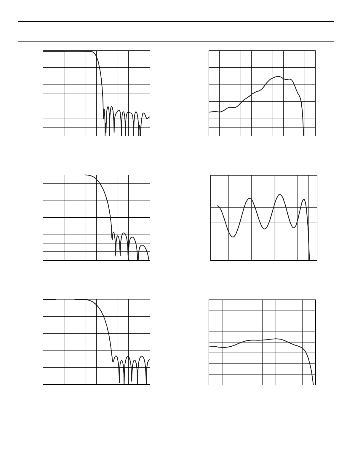
Figure 14. ADC Decimation Filter, 128× Oversampling, Normalized to f
07680-010
S
0.10
0.08
0.06
0.04
0.02
0
–0.02
MAGNITUDE (d BFS)
–0.04
–0.06
–0.08
–0.10
0 0.05 0.10 0.20 0.30 0.400.15 0.25 0.35 0.500.45
FREQUENCY (NORMALIZED TO
f
)
S
Figure 17. ADC Decimation Filter Pass-Band Ripple, 128× Oversampling,
Normalized to f
S
07680-011
0
–10
–20
–30
–40
–50
–60
MAGNITUDE (d BFS)
–70
–80
–90
–100
0
0.1 0.2 0.3 0.4 0.5 0.6 0.7 0.8 0.9 1.0
FREQUENCY (NORMALIZED TO
f
)
S
07680-012
Figure 15. ADC Decimation Filter, 128× Oversampling, Double-Rate Mode,
Normalized to f
0
10
20
30
40
50
60
MAGNITUDE (dBFS)
70
80
90
100
0 0.1 0.2 0.3 0.4 0.5 0.6 0.7 0.8 0.9 1.0
FREQUENCY (NORMALIZED TO
S
f
)
S
7680-014
Figure 16. DAC Interpolation Filter, 64× Oversampling, Double-Rate Mode,
Normalized to f
S
0.04
0.02
0
0.02
MAGNITUDE (dBFS)
0.04
0.06
0 0.05 0.10 0.20 0.30 0.400.15 0.25 0.35
FREQUENCY (NO RMALIZED T O
f
)
S
Figure 18. ADC Decimation Filter Pass-Band Ripple, 128× Oversampling,
Double-Rate Mode, Normalized to f
0.20
0.15
0.10
0.05
0
–0.05
MAGNITUDE (dBFS)
–0.10
–0.15
–0.20
0 0.05 0.10 0.20 0.30 0.400.15 0.25 0.35
FREQUENCY (NORMALIZED TO
S
f
)
S
Figure 19. DAC Interpolation Filter Pass-Band Ripple, 64× Oversampling,
Double-Rate Mode, Normalized to f
S
07680-013
07680-015
Rev. C | Page 18 of 92
ADAU1761
0
–10
–20
–30
–40
–50
–60
MAGNITUDE (dBFS)
–70
–80
–90
–100
0.10 0.20.30.40.50.60.70.80.91.0
FREQUENCY (NORMALIZED TO
f
)
S
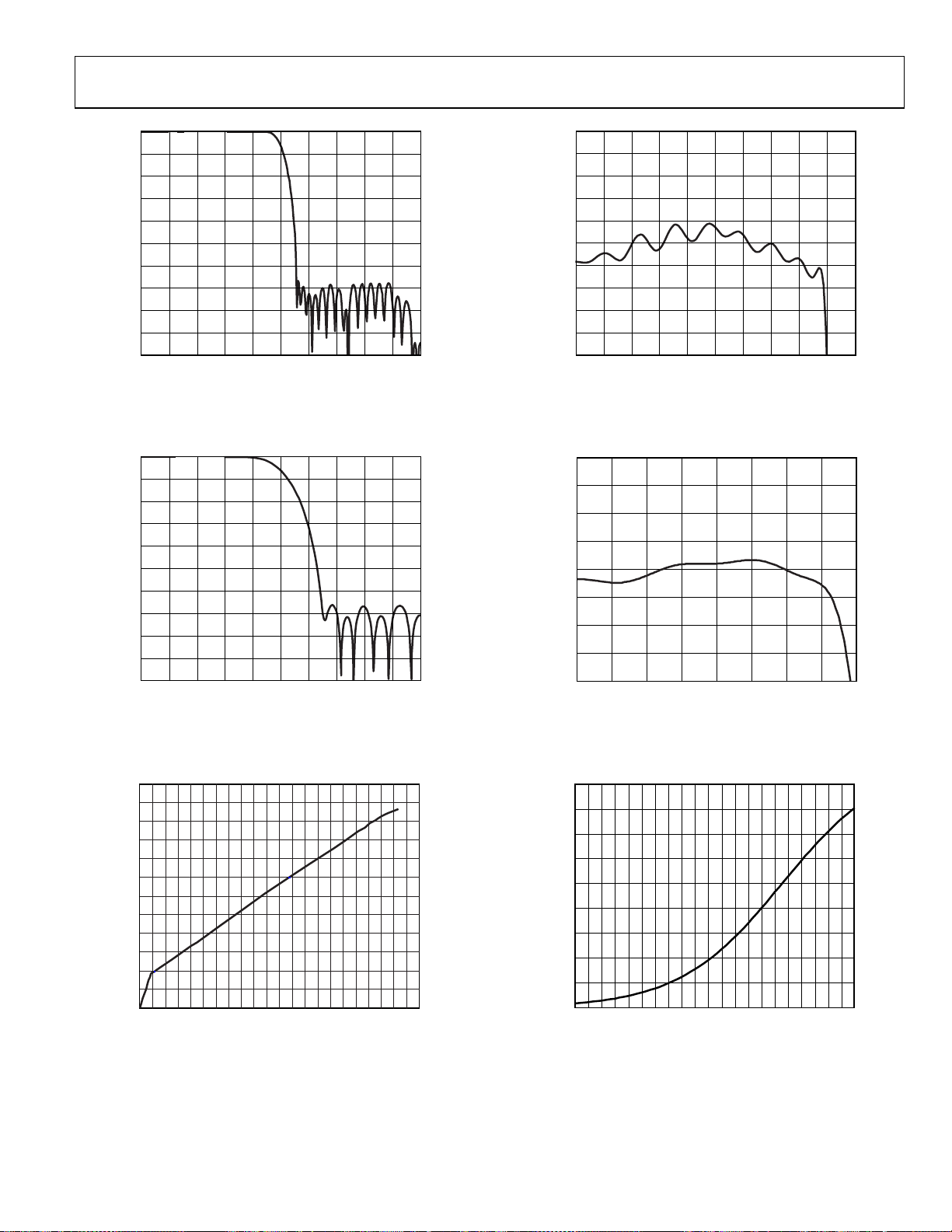
Figure 20. DAC Interpolation Filter, 128× Oversampling, Normalized to f
0
10
20
30
40
50
60
MAGNITUDE (dBFS)
70
80
90
100
0.10 0.2 0.3 0.4 0.5 0.6 0.7 0.8 0.9 1.0
FREQUENCY (NORMALIZED TO
f
)
S
Figure 21. DAC Interpolation Filter, 128× Oversampling, Double-Rate Mode,
Normalized to fS
0.05
0.04
0.03
0.02
0.01
0
–0.01
MAGNITUDE (dBFS)
–0.02
–0.03
–0.04
–0.05
0 0.05 0.10 0.20 0.30 0.400. 15 0.25 0.35 0.500.45
7680-016
Figure 23. DAC Interpolation Filter Pass-Band Ripple, 128× Oversampling,
S
FREQUENCY (NORMALIZED TO
Normalized to f
0.20
0.15
0.10
0.05
0
–0.05
MAGNITUDE (d BFS)
–0.10
–0.15
–0.20
0 0.05 0.10 0.20 0.30 0.400.15 0.25 0. 35
07680-018
FREQUENCY (NO RMALIZED T O
f
)
S
S
f
)
S
Figure 24. DAC Interpolation Filter Pass-Band Ripple, 128× Oversampling,
Double-Rate Mode, Normalized to f
S
07680-017
07680-019
12
11
10
9
8
7
6
5
CURRENT (mA)
4
3
2
1
0
0 100 200 300 400 500 600 700 800 900 1000 1100
INSTRUCTIO NS
7680-065
90
80
70
60
50
40
IMPEDANCE (k)
30
20
10
0
8.00
5.75
3.50
35.00
32.75
30.50
28.25
26.00
23.75
21.50
19.25
17.00
14.75
12.50
10.25
GAIN (dB)
1.25
–1.00
–3.25
–5.50
–7.75
–10.00
–12.25
7680-125
Figure 25. Input Impedance vs. Gain for Analog Inputs Figure 22. Typical DSP Current Draw
Rev. C | Page 19 of 92
ADAU1761
SYSTEM BLOCK DIAGRAMS
FROM VOLTAGE
REGULATOR
THE INPUT CAPACI TOR VALUE DE PENDS ON THE
INPUT IMPE DANCE, WHICH VARI ES WITH THE
VOLUME SETTING.
10µF
LEFT
MICROPHONE
10µF
2k
2k
10µF
LINP
LINN
MICBIAS
10µF
0.1µF
(1.8V TO 3.3V)
10µF
++
0.1µF
AVDDIOVDD AVDDDVDDOUT
ADAU1761
1.2nH
LOUTP
LOUTN
RHP
MONOOUT
LHP
ROUTP
ROUTN
10µF
+
0.1µF
0.1µF
9.1pF
EARPIECE
SPEAKER
CAPLESS
HEADPHONE
OUTPUT
EARPIECE
SPEAKER
RIGHT
MICROPHONE
AUX LEFT
AUX RIGHT
1k
1k
10µF
JACK
DETECTIO N
SIGNAL
CLOCK
SOURCE
10µF
10µF
49.9
RINN
RINP
JACKDET/MICI N
LAUX
RAUX
MCLK
DGND
AGND
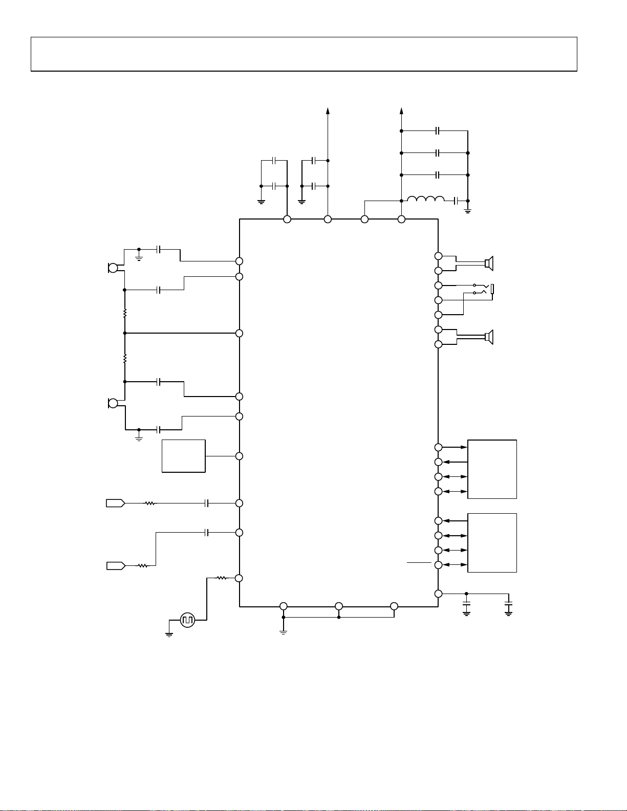
Figure 26. System Block Diagram
ADC_SDATA/GPIO 1
DAC_SDATA/GPIO 0
LRCLK/GPI O3
BCLK/GPIO 2
ADDR1/CDATA
SDA/COUT
SCL/CCLK
ADDR0/CLATCH
CM
AGND
SERIAL DATA
SYSTEM
CONTRO LLER
0.1µF 10µF
+
07680-045
Rev. C | Page 20 of 92
ADAU1761
THE INPUT CAPACI TOR VALUE DE PENDS ON THE
INPUT IMPE DANCE, WHICH VARI ES WITH THE
VOLUME SETTING.
V
DD
SINGLE-ENDED
ANALOG
MICROPHONE
GND
V
DD
SINGLE-ENDED
ANALOG
MICROPHONE
GND
OUTPUT
OUTPUT
10µF
CM
10µF
CM
10µF
0.1µF
MICBIAS
LINN
LINP
RINN
RINP
10µF
0.1µF
FROM VOLTAGE
(1.8V TO 3.3V)
++
ADAU1761
REGULATOR
AVDDIOVDD AVDDDVDDOUT
1.2nH
LOUTP
LOUTN
RHP
MONOOUT
LHP
ROUTP
ROUTN
10µF
+
0.1µF
0.1µF
9.1pF
EARPIECE
SPEAKER
CAPLESS
HEADPHONE
OUTPUT
EARPIECE
SPEAKER
AUX LEFT
AUX RIGHT
1k
1k
JACK
DETECT ION
SIGNAL
CLOCK
SOURCE
ADC_SDATA/GPI O1
DAC_SDATA/GPI O0
10µF
10µF
49.9
JACKDET/MICI N
LAUX
RAUX
MCLK
DGND
AGND
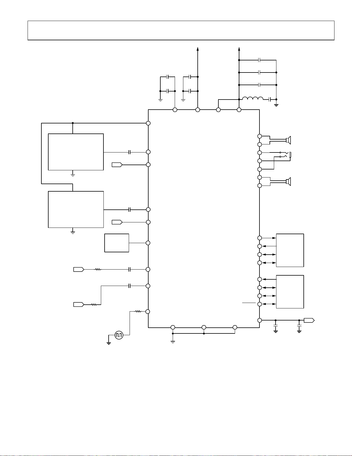
Figure 27. System Block Diagram with Analog Microphones
LRCLK/GPIO3
BCLK/G PIO2
ADDR1/CDATA
SDA/CO UT
SCL/CCLK
ADDR0/CLATCH
CM
AGND
SERIAL DATA
SYSTEM
CONTROLL ER
0.1µF 10µF
+
07680-059
Rev. C | Page 21 of 92
ADAU1761
R
R
10µF
0.1µF
MICBIAS
LINP
LINN
RINN
RINP
JACKDET/MICI N
LAUX
RAUX
MCLK
0.1µF
0.1µF
V
DD
V
DD
AUX LEFT
AUX RIGHT
CLK
DIGITAL
MICROPHONE
CLK
DIGITAL
MICROPHONE
1k
1k
BCLK
CM
DATA
GNDL/R SELECT
BCLK
DATA
GNDL/R SELECT
10µF
10µF
49.9
FROM VOLTAGE
10µF
++
0.1µF
ADAU1761
REGULATOR
(1.8V TO 3.3V)
AVDDIOVDD AVDDDVDDOUT
ADC_SDATA/GPI O1
DAC_SDATA/GPI O0
LRCLK/GPI O3
ADDR1/CDATA
ADDR0/CLATCH
1.2nH
RHP
MONOOUT
LHP
LOUTP
LOUTN
ROUTP
ROUTN
BCLK/GPIO2
SDA/COUT
SCL/CCLK
10µF
+
0.1µF
0.1µF
9.1pF
CAPLESS
HEADPHONE
OUTPUT
22nF
22nF
22nF
22nF
10µF
R
EXT
INL+
R
EXT
INL–
R
EXT
INR+
R
EXT
INR–
SERIAL DATA
SYSTEM
CONTROLL ER
2.5V TO 5. 0V
0.1µF
VDDVDD
SSM2306
CLASS-D 2W
STEREO SPEAKER
DRIVER
GNDSD GND
SHUTDOWN
OUTL+
OUTL–
OUTR+
OUTR–
LEFT
SPEAKE
RIGHT
SPEAKE
CLOCK
SOURCE
DGND
AGND
AGND
CM
0.1µF 10µF
+
07680-060
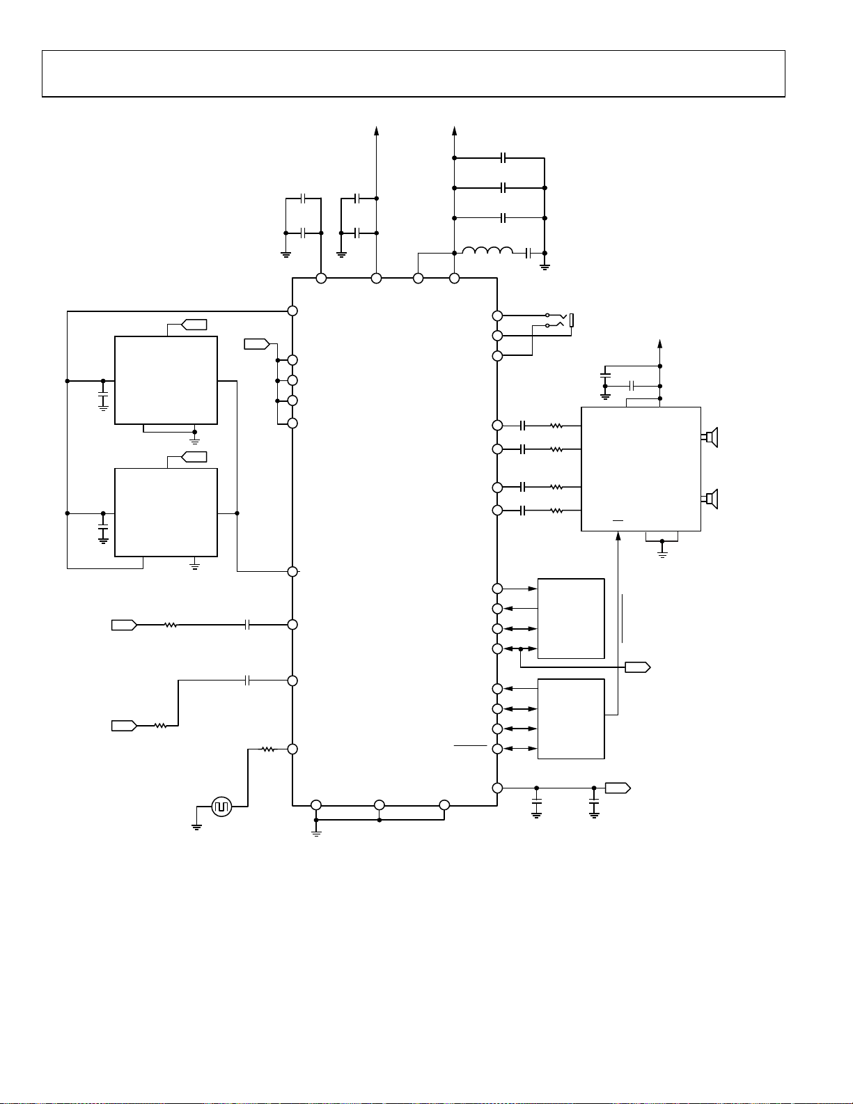
Figure 28. System Block Diagram with Digital Microphones and SSM2306 Class-D Speaker Driver
Rev. C | Page 22 of 92

ADAU1761
THEORY OF OPERATION
The ADAU1761 is a low power audio codec with an integrated
stream-oriented DSP core, making it an all-in-one package that
offers high quality audio, low power, small size, and many
advanced features. The stereo ADC and stereo DAC each have
an SNR of at least +98 dB and a THD + N of at least −90 dB.
The serial data port is compatible with I
justified, and TDM modes for interfacing to digital audio data.
The operating voltage range is 1.8 V to 3.65 V, with an on-board
regulator generating the internal digital supply voltage.
The record signal path includes very flexible input configurations
that can accept differential and single-ended analog microphone
inputs as well as a digital microphone input. A microphone bias
pin provides seamless interfacing to electret microphones. Input
configurations can accept up to six single-ended analog signals
or variations of stereo differential or stereo single-ended signals
with two additional auxiliary single-ended inputs. Each input
signal has its own programmable gain amplifier (PGA) for volume
adjustment and can be routed directly to the playback path output
mixers, bypassing the ADCs. An automatic level control (ALC)
can also be implemented to keep the recording volume constant.
The ADCs and DACs are high quality, 24-bit Σ- converters
that operate at selectable 64× or 128× oversampling ratios. The
base sampling rate of the converters is set by the input clock rate
and can be further scaled with the converter control register
settings. The converters can operate at sampling frequencies
from 8 kHz to 96 kHz. The ADCs and DACs also include very
fine-step digital volume controls.
The playback path allows input signals and DAC outputs to be
mixed into various output configurations. Headphone drivers
are available for a stereo headphone output, and the other output
pins are capable of differentially driving an earpiece speaker.
Capless headphone outputs are possible with the use of the
mono output as a virtual ground connection. The stereo line
outputs can be used as either single-ended or differential
outputs and as an optional mix-down mono output.
The DSP core introduces many features that make this codec
unique and optimized for audio processing. The program and
parameter RAMs can be loaded with custom audio processing
signal flow built using the SigmaStudio graphical programming
software from Analog Devices, Inc. The values stored in the
parameter RAM control individual signal processing blocks,
such as equalization filters, dynamics processors, audio delays,
and mixer levels.
2
S, left-justified, right-
The SigmaStudio software is used to program and control the
SigmaDSP through the control port. Along with designing and
tuning a signal flow, the tools can be used to configure all of the
DSP registers. The SigmaStudio graphical interface allows anyone with digital or analog audio processing knowledge to easily
design DSP signal flow and port it to a target application. At the
same time, it provides enough flexibility and programmability
for an experienced DSP programmer to have in-depth control
of the design. In SigmaStudio, the user can connect graphical
blocks (such as biquad filters, dynamics processors, mixers, and
delays), compile the design, and load the program and parameter
files into the ADAU1761 memory through the control port.
Signal processing blocks available in the provided libraries
include the following:
• Enhanced stereo capture
• Single- and double-precision biquad filters
• FIR filters
• Dynamics processors with peak or rms detection for mono
and multichannel dynamics
• Mixers and splitters
• Tone and noise generators
• Fixed and variable gain
• Loudness
• Delay
• Stereo enhancement
• Dynamic bass boost
• Noise and tone sources
• Level detectors
Additional processing blocks are always being developed.
Analog Devices also provides proprietary and third-party
algorithms for applications such as matrix decoding, bass
enhancement, and surround virtualizers. Contact Analog
Devices (
these algorithms.
The ADAU1761 can generate its internal clocks from a wide
range of input clocks by using the on-board fractional PLL.
The PLL accepts inputs from 8 MHz to 27 MHz.
The ADAU1761 is provided in a small, 32-lead, 5 mm × 5 mm
LFCSP with an exposed bottom pad.
www.analog.com) for information about licensing
Rev. C | Page 23 of 92
ADAU1761
STARTUP, INITIALIZATION, AND POWER
This section describes the procedure for properly starting up
the ADAU1761. The following sequence provides a high level
approach to the proper initiation of the system.
1. Apply power to the ADAU1761.
2. Lock the PLL to the input clock (if using the PLL).
3. Enable the core clock.
4. Load the register settings.
See the Startup section for more information about the proper
start-up sequence.
POWER-UP SEQUENCE
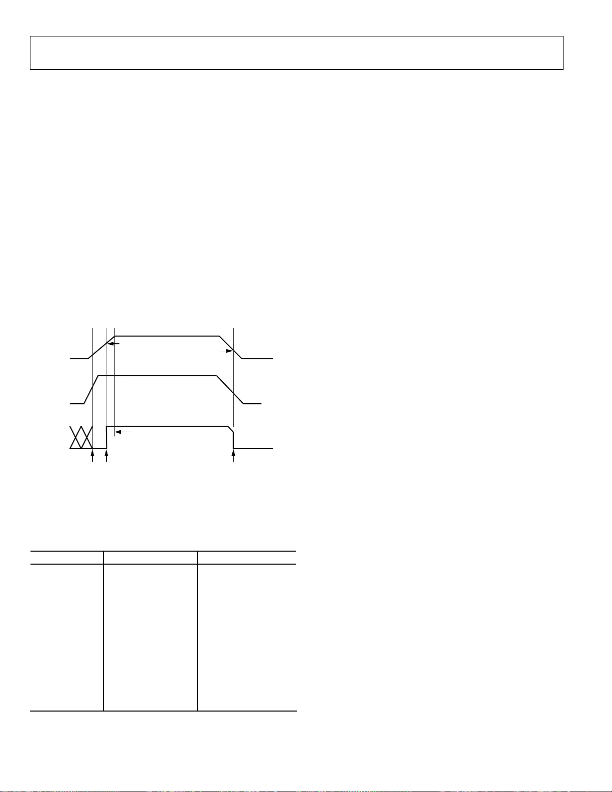
The ADAU1761 uses a power-on reset (POR) circuit to
reset the registers upon power-up. The POR monitors the
DVDDOUT pin and generates a reset signal whenever power
is applied to the chip. During the reset, the ADAU1761 is set
to the default values documented in the register map (see the
Control Registers section). Typically, with a 10 F capacitor on
AVDD, the POR takes approximately 14 ms.
1.5V
DVDDOUT
1.35V
0.95V
POWER REDUCTION MODES
Sections of the ADAU1761 chip can be turned on and off as
needed to reduce power consumption. These include the ADCs,
the DACs, the PLL, and the DSP core.
In addition, the control registers can be used to configure some
functions for power saving, normal, or enhanced performance
operation. See the Control Registers section for more
information.
The digital filters of the ADCs and DACs can each be set to oversampling ratios of 64× or 128× (default). Setting the oversampling
ratios to 64× for these filters lowers power consumption with a
minimal impact on performance. See the Digital Filters section
for specifications; see the Typical Performance Characteristics
section for graphs of these filters.
DIGITAL POWER SUPPLY
The digital power supply for the ADAU1761 is generated from
an internal regulator. This regulator generates a 1.5 V supply
internally. The only external connection to this regulator is the
DVDDOUT bypassing point. A 100 nF capacitor and a 10 F
capacitor should be connected between this pin and DGND.
AVDD
POR
FINISHED
PART READY
POR ACTIVE
POR
POR
ACTIVE
Figure 29. Power-On Reset Sequence
The PLL lock time is dependent on the MCLK rate. Typical
lock times are provided in Tab l e 1 1 . The DSP can be enabled
immediately after the PLL is locked.
Table 11. PLL Lock Times
PLL Mode MCLK Frequency Lock Time (Typical)
Fractional 8 MHz 3.5 ms
Fractional 12 MHz 3.0 ms
Integer 12.288 MHz 2.96 ms
Fractional 13 MHz 2.4 ms
Fractional 14.4 MHz 2.4 ms
Fractional 19.2 MHz 2.98 ms
Fractional 19.68 MHz 2.98 ms
Fractional 19.8 MHz 2.98 ms
Fractional 24 MHz 2.95 ms
Integer 24.576 MHz 2.96 ms
Fractional 26 MHz 2.4 ms
Fractional 27 MHz 2.4 ms
INPUT/OUTPUT POWER SUPPLY
The power for the digital output pins is supplied from IOVDD,
and this pin also sets the highest input voltage that should be
seen on the digital input pins. IOVDD should be set between
1.8 V and 3.3 V; no digital input signal should be at a voltage
level higher than the one on IOVDD. The current draw of this
pin is variable because it depends on the loads of the digital
7680-061
outputs. IOVDD should be decoupled to DGND with a 100 nF
capacitor and a 10 F capacitor.
CLOCK GENERATION AND MANAGEMENT
The ADAU1761 uses a flexible clocking scheme that enables the
use of many different input clock rates. The PLL can be bypassed
or used, resulting in two different approaches to clock management. For more information about clocking schemes, PLL
configuration, and sampling rates, see the Clocking and
Sampling Rates section.
Case 1: PLL Is Bypassed
If the PLL is bypassed, the core clock is derived directly from
the MCLK input. The rate of this clock must be set properly in
Register R0 (clock control register, Address 0x4000) using the
INFREQ[1:0] bits. When the PLL is bypassed, supported external
clock rates are 256 × f
is the base sampling rate. The core clock of the chip is off until
the core clock enable bit (COREN) is asserted. If a clock slower
than 1024 × f
is directly input to the ADAU1761 (bypassing the
S
PLL), the number of available SigmaDSP processing cycles is
reduced and the DSPSR bits in Register R57 (Address 0x40EB)
should be adjusted accordingly.
, 512 × fS, 768 × fS, and 1024 × fS, where fS
S
Rev. C | Page 24 of 92

ADAU1761
Case 2: PLL Is Used
The core clock to the entire chip is off during the PLL lock
acquisition period. The user can poll the lock bit to determine
when the PLL has locked. After lock is acquired, the ADAU1761
can be started by asserting the core clock enable bit (COREN)
in Register R0 (clock control register, Address 0x4000). This bit
enables the core clock to all the internal blocks of the ADAU1761.
PLL Lock Acquisition
During the lock acquisition period, only Register R0 (Address
0x4000) and Register R1 (Address 0x4002) are accessible through
the control port. Because all other registers require a valid master
clock for reading and writing, do not attempt to access any other
register. Any read or write is prohibited until the core clock
enable bit (COREN) and the lock bit are both asserted.
To program the PLL during initialization or reconfiguration of
the clock setting, the following procedure must be followed:
1. Power down the PLL.
2. Reset the PLL control register.
3. Start the PLL.
4. Poll the lock bit.
5. Assert the core clock enable bit after the PLL lock
is acquired.
The PLL control register (Register R1, Address 0x4002) is a
48-bit register where all bits must be written with a single
continuous write to the control port.
Rev. C | Page 25 of 92
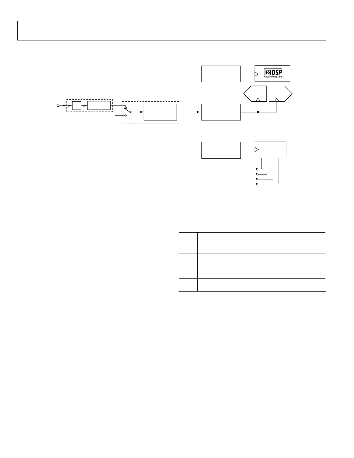
ADAU1761
G
CLOCKING AND SAMPLING RATES
R1: PLL CONT ROL REGISTER
MCLK
÷ X
× (R + N/M)
CLKSRC
CORE CLOCK
Clocks for the converters, the serial ports, and the DSP are
derived from the core clock. The core clock can be derived
directly from MCLK or it can be generated by the PLL. The
CLKSRC bit (Bit 3 in Register R0, Address 0x4000) determines
the clock source.
The INFREQ[1:0] bits should be set according to the expected
input clock rate selected by CLKSRC; this value also determines
the core clock rate and the base sampling frequency, f
For example, if the input to CLKSRC = 49.152 MHz (from
PLL), then
INFREQ[1:0] = 1024 × f
f
= 49.152 MHz/1024 = 48 kHz
S
The PLL output clock rate is always 1024 × f
control register automatically sets the INFREQ[1:0] bits to
1024 × f
when using the PLL. When using a direct clock, the
S
INFREQ[1:0] frequency should be set according to the MCLK
pin clock rate and the desired base sampling frequency.
S
, and the clock
S
R0: CLOCK
CONTROL REGISTER
INFREQ[1:0]
256 ×
f
768 ×
f
S
Figure 30. Clock Tree Diagram
.
S
, 512 ×
S
, 1024 ×
R57: DSP SAMPLIN
RATE SETTING
DSPSR[3:0]
f
/0.5, 1, 1.5, 2, 3, 4, 6
S
R17: CONVERTER
CORE
CLOCK
f
,
S
f
S
SAMPLING RAT E
CONVSR[2:0]
f
/0.5, 1, 1.5, 2, 3, 4, 6
S
R64: SERIAL PO RT
SAMPLING RAT E
SPSR[2:0]
f
/0.5, 1, 1.5, 2, 3, 4, 6
S
ADC_SDATA/GPI O1
DAC_SDATA/GPI O0
BCLK/GPI O2
LRCLK/GPIO3
ADCs
DACs
SERIAL
DATA INPUT/
OUTPUT PO RT
To utilize the maximum amount of DSP instructions, the core
clock should run at a rate of 1024 × f
.
S
Table 12. Clock Control Register (Register R0, Address 0x4000)
Bits Bit Name Settings
3 CLKSRC
0: Direct from MCLK pin (default)
1: PLL clock
[2:1] INFREQ[1:0]
0 COREN
00: 256 × f
01: 512 × f
10: 768 × f
11: 1024 × f
0: Core clock disabled (default)
(default)
S
S
S
S
1: Core clock enabled
07680-020
Rev. C | Page 26 of 92

ADAU1761
SAMPLING RATES
The ADCs, DACs, and serial port share a common sampling
rate that is set in Register R17 (Converter Control 0 register,
Address 0x4017). The CONVSR[2:0] bits set the sampling rate
as a ratio of the base sampling frequency. The DSP sampling
rate is set in Register R57 (DSP sampling rate setting register,
Address 0x40EB) using the DSPSR[3:0] bits, and the serial port
sampling rate is set in Register R64 (serial port sampling rate
register, Address 0x40F8) using the SPSR[2:0] bits.
It is recommended that the sampling rates for the converters,
serial ports, and DSP be set to the same value, unless appropriate
compensation filtering is done within the DSP. Tab l e 1 3 and
Tabl e 1 4 list the sampling rate divisions for common base
sampling rates.
Table 13. 48 kHz Base Sampling Rate Divisions
Base Sampling
Frequency Sampling Rate Scaling Sampling Rate
fS = 48 kHz
Table 14. 44.1 kHz Base Sampling Rate Divisions
Base Sampling
Frequency Sampling Rate Scaling Sampling Rate
fS = 44.1 kHz
fS/1 48 kHz
fS/6 8 kHz
fS/4 12 kHz
fS/3 16 kHz
fS/2 24 kHz
fS/1.5 32 kHz
fS/0.5 96 kHz
fS/1 44.1 kHz
fS/6 7.35 kHz
fS/4 11.025 kHz
fS/3 14.7 kHz
fS/2 22.05 kHz
fS/1.5 29.4 kHz
fS/0.5 88.2 kHz
PLL
The PLL uses the MCLK as a reference to generate the core
clock. PLL settings are set in Register R1 (PLL control register,
Address 0x4002). Depending on the MCLK frequency, the PLL
must be set for either integer or fractional mode. The PLL can
accept input frequencies in the range of 8 MHz to 27 MHz.
All six bytes in the PLL control register must be written with a
single continuous write to the control port.
TO PLL
MCLK
÷ X
× (R + N/M)
Figure 31. PLL Block Diagram
Integer Mode
Integer mode is used when the MCLK is an integer (R) multiple
of the PLL output (1024 × f
).
S
For example, if MCLK = 12.288 MHz and f
PLL required output = 1024 × 48 kHz = 49.152 MHz
R = 49.152 MHz/12.288 MHz = 4
In integer mode, the values set for N and M are ignored.
Fractional Mode
Fractional mode is used when the MCLK is a fractional
(R + (N/M)) multiple of the PLL output.
For example, if MCLK = 12 MHz and f
PLL required output = 1024 × 48 kHz = 49.152 MHz
R + (N/M) = 49.152 MHz/12 MHz = 4 + (12/125)
Common fractional PLL parameter settings for 44.1 kHz and
48 kHz sampling rates can be found in Table 16 and Ta b le 1 7.
The PLL outputs a clock in the range of 41 MHz to 54 MHz,
which should be taken into account when calculating PLL
values and MCLK frequencies.
CLOCK DIVIDER
= 48 kHz, then
S
= 48 kHz, then
S
07680-021
Table 15. PLL Control Register (Register R1, Address 0x4002)
Bits Bit Name Description
[47:32] M[15:0] Denominator of the fractional PLL: 16-bit binary number
0x00FD: M = 253 (default)
[31:16] N[15:0] Numerator of the fractional PLL: 16-bit binary number
0x000C: N = 12 (default)
[14:11] R[3:0] Integer part of PLL: four bits, only values 2 to 8 are valid
0010: R = 2 (default)
0011: R = 3
0100: R = 4
0101: R = 5
0110: R = 6
0111: R = 7
1000: R = 8
Rev. C | Page 27 of 92

ADAU1761
Bits Bit Name Description
[10:9] X[1:0] PLL input clock divider
00: X = 1 (default)
01: X = 2
10: X = 3
11: X = 4
8 Type PLL operation mode
0: Integer (default)
1: Fractional
1 Lock PLL lock (read-only bit)
0: PLL unlocked (default)
1: PLL locked
0 PLLEN PLL enable
0: PLL disabled (default)
1: PLL enabled
Table 16. Fractional PLL Parameter Settings for f
= 44.1 kHz (PLL Output = 45.1584 MHz = 1024 × fS)
S
MCLK Input (MHz) Input Divider (X) Integer (R) Denominator (M) Numerator (N) R2: PLL Control Setting (Hex)
8 1 5 625 403 0x0271 0193 2901
12 1 3 625 477 0x0271 01DD 1901
13 1 3 8125 3849 0x1FBD 0F09 1901
14.4 2 6 125 34 0x007D 0022 3301
19.2 2 4 125 88 0x007D 0058 2301
19.68 2 4 1025 604 0x0401 025C 2301
19.8 2 4 1375 772 0x055F 0304 2301
24 2 3 625 477 0x0271 01DD 1B01
26 2 3 8125 3849 0x1FBD 0F09 1B01
27 2 3 1875 647 0x0753 0287 1B01
Table 17. Fractional PLL Parameter Settings for f
= 48 kHz (PLL Output = 49.152 MHz = 1024 × fS)
S
MCLK Input (MHz) Input Divider (X) Integer (R) Denominator (M) Numerator (N) R2: PLL Control Setting (Hex)
8 1 6 125 18 0x007D 0012 3101
12 1 4 125 12 0x007D 000C 2101
13 1 3 1625 1269 0x0659 04F5 1901
14.4 2 6 75 62 0x004B 003E 3301
19.2 2 5 25 3 0x0019 0003 2B01
19.68 2 4 205 204 0x00CD 00CC 2301
19.8 2 4 825 796 0x0339 031C 2301
24 2 4 125 12 0x007D 000C 2301
26 2 3 1625 1269 0x0659 04F5 1B01
27 2 3 1125 721 0x0465 02D1 1B01
Table 18. Integer PLL Parameter Settings for f
= 48 kHz (PLL Output = 49.152 MHz = 1024 × fS)
S
MCLK Input (MHz) Input Divider (X) Integer (R) Denominator (M) Numerator (N) R2: PLL Control Setting (Hex)1
12.288 1 4 Don’t care Don’t care 0xXXXX XXXX 2001
24.576 1 2 Don’t care Don’t care 0xXXXX XXXX 1001
1
X = don’t care.
Rev. C | Page 28 of 92
 Loading...