www.BDTIC.com/ADI
Class-D Audio Power Amplifier
FEATURES
Integrated stereo modulator and power stage
0.005% THD + N
101 dB dynamic range
PSRR > 65 dB
R
< 0.3 Ω (per transistor)
DS-ON
Efficiency > 90% (8 Ω)
EMI-optimized modulator
On/off-mute pop-noise suppression
Short-circuit protection
Overtemperature protection
APPLICATIONS
Flat panel televisions
PC audio systems
Mini-components
PGA0 PGA1
AINL
SLC_TH
AINR
AVD D
VREF
AGND
DVDD
DGND
PGA
SLICER
PGA
PGA0 PGA1
VOLTAGE
REFERENCE
GENERAL DESCRIPTION
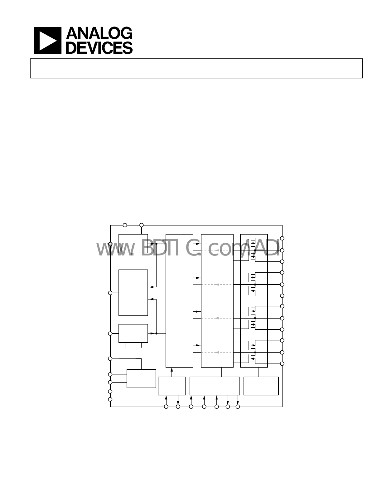
The ADAU1592 is a 2-channel, bridge-tied load (BTL)
switching audio power amplifier with an integrated Σ-
modulator.
The modulator accepts an analog input signal and generates
tching output to drive speakers directly. A digital,
a swi
microcontroller-compatible interface provides control of reset,
mute, and PGA gain as well as output signals for thermal and
overcurrent error conditions. The output stage can operate
from supply voltages ranging from 9 V to 18 V. The analog
modulator and digital logic operate from a 3.3 V supply.
FUNCTIONAL BLOCK DIAGRAM
MODE CO NTROL
Figure 1.
LEVEL SHIFT
AND DEAD
TIME CONT ROL
LOGIC
OTWXTOXTI ERRMUTESTDN
Σ-Δ
MODULATOR
f
/2
CLK
CLOCK
OSCILLATOR
MO/ST
A1
A2
B1
B2
C1
C2
D1
D2
TEMPERATURE/
OVERCURRENT
PROTECTION
ADAU1592
PVDD
OUTL+
PGND
PVDD
OUTL–
PGND
PVDD
OUTR+
PGND
PVDD
OUTR–
PGND
ADAU1592
06749-001
Rev. A
Information furnished by Analog Devices is believed to be accurate and reliable. However, no
responsibility is assumed by Anal og Devices for its use, nor for any infringements of patents or ot her
rights of third parties that may result from its use. Specifications subject to change without notice. No
license is granted by implication or otherwise under any patent or patent rights of Analog Devices.
Trademarks and registered trademarks are the property of their respective owners.
One Technology Way, P.O. Box 9106, Norwood, MA 02062-9106, U.S.A.
Tel: 781.329.4700 www.analog.com
Fax: 781.461.3113 ©2007 Analog Devices, Inc. All rights reserved.

ADAU1592
www.BDTIC.com/ADI
TABLE OF CONTENTS
Features.............................................................................................. 1
Applications....................................................................................... 1
General Description ......................................................................... 1
Functional Block Diagram .............................................................. 1
Revision History ............................................................................... 2
Specifications..................................................................................... 3
Audio Performance ...................................................................... 3
DC Specifications ......................................................................... 4
Power Supplies .............................................................................. 4
Digital I/O ..................................................................................... 4
Digital Timing............................................................................... 5
Absolute Maximum Ratings............................................................ 6
Thermal Resistance ...................................................................... 6
ESD Caution.................................................................................. 6
Pin Configuration and Function Descriptions............................. 7
Typical Performance Characteristics ............................................. 9
Theory of Operation ...................................................................... 15
Overview...................................................................................... 15
Modulator.................................................................................... 15
Slicer............................................................................................. 15
Power Stage ................................................................................. 16
Gain.............................................................................................. 16
Protection Circuits..................................................................... 16
Thermal Protection.................................................................... 16
Overcurrent Protection ............................................................. 16
Undervoltage Protection ........................................................... 17
Clock Loss Detection ................................................................. 17
Automatic Recovery from Protections.................................... 17
and
STDN
...................................................................... 17
REF
and C
.............................................. 19
IN
MUTE
Power-Up/Power-Down Sequence .......................................... 18
DC Offset and Pop Noise.......................................................... 19
Selecting Values for C
Mono Mode................................................................................. 19
Power Supply Decoupling......................................................... 19
External Protection for PVDD > 15 V .................................... 20
Clock ............................................................................................ 20
Applications Information.............................................................. 21
Outline Dimensions....................................................................... 23
Ordering Guide .......................................................................... 23
REVISION HISTORY
9/07—Rev. 0 to Rev. A
Changes to Figure 14, Figure 15, and Figure 16 ......................... 10
Changes to Applications Information Section............................ 21
Changes to Ordering Guide.......................................................... 23
5/07—Revision 0: Initial Version
Rev. A | Page 2 of 24
ADAU1592
www.BDTIC.com/ADI
SPECIFICATIONS
AVDD = 3.3 V, DVDD = 3.3 V, PVDD = 15 V, ambient temperature = 25°C, load impedance = 6 , clock frequency = 24.576 MHz,
measurement bandwidth = 20 Hz to 20 kHz, unless otherwise specified.
AUDIO PERFORMANCE
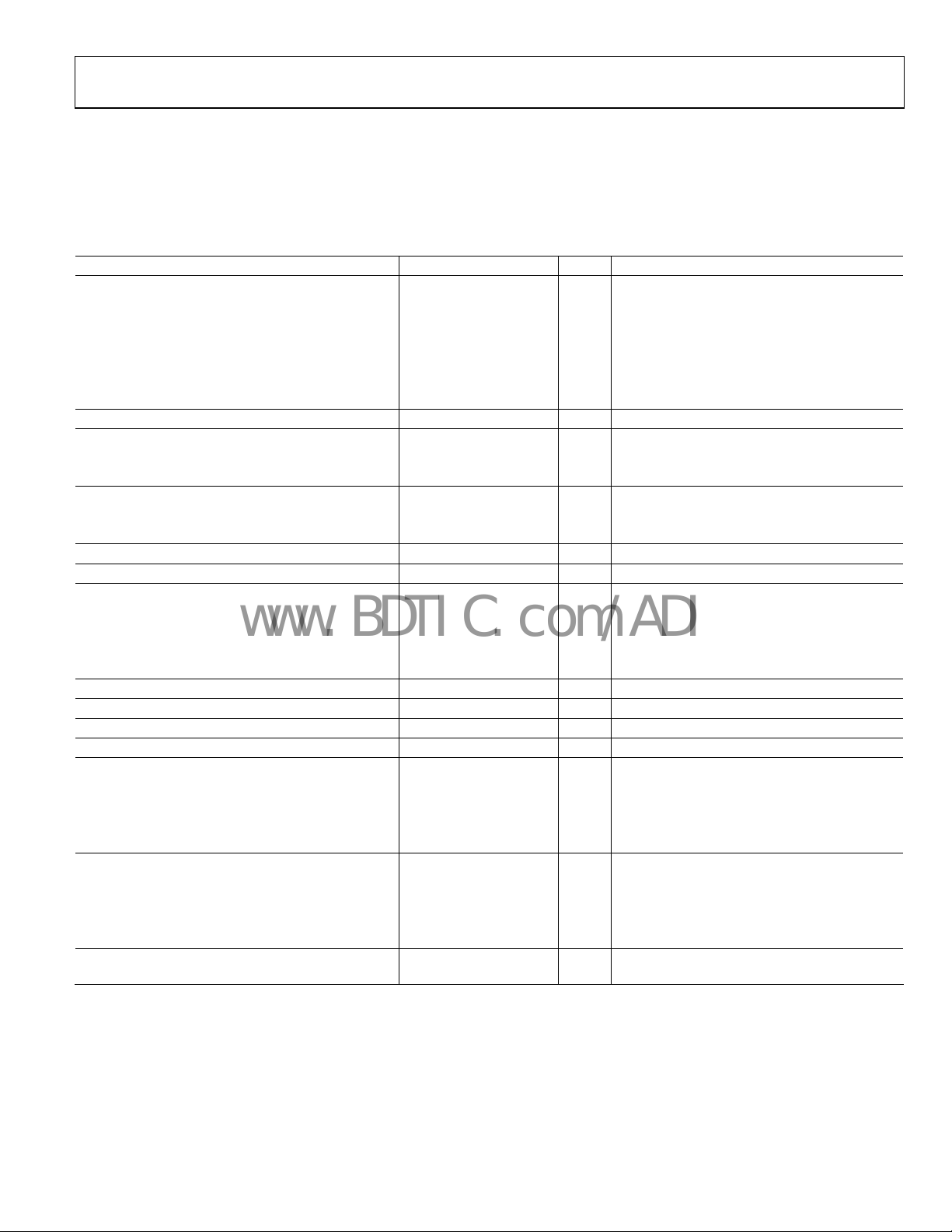
Table 1.
Parameter Min Typ Max Unit Test Conditions/Comments
OUTPUT POWER
12 W 1% THD + N, 8 Ω
15 W 10% THD + N, 8 Ω
14.5 W 1% THD + N, 6 Ω
18 W 10% THD + N, 6 Ω
19.5 W 1% THD + N, 4 Ω
24 W 10% THD + N, 4 Ω
EFFICIENCY 87 % @ 18 W, 6 Ω
R
@ T
DS-ON
Per High-Side Transistor 0.28 Ω @ 100 mA
Per Low-Side Transistor 0.25 Ω @ 100 mA
THERMAL CHARACTERISTICS
Thermal Warning Active
Thermal Shutdown Active 150 °C Die temperature
OVERCURRENT SHUTDOWN ACTIVE 5 6 A Peak current
PVDD UNDERVOLTAGE SHUTDOWN 5.1 V
INPUT LEVEL FOR FULL-SCALE OUTPUT Full-scale output @ 1% THD + N
1.0 V
0.5 V
0.25 V
0.125 V
TOTAL HARMONIC DISTORTION + NOISE (THD + N) 0.005 % 1 kHz, P
SIGNAL-TO-NOISE RATIO (SNR) 99 101 dB A-weighted, referred to 1% THD + N output
DYNAMIC RANGE (DNR) 99 101 dB A-weighted, measured with −60 dBFS input
CROSSTALK (LEFT TO RIGHT OR RIGHT TO LEFT) −90 dB @ full-scale output voltage, 1% THD + N, 1 kHz
AMPLIFIER GAIN PVDD = 15 V, 6 Ω
PGA = 0 dB 19 dB
PGA = 6 dB 25 dB
PGA = 12 dB 31 dB
PGA = 18 dB 37 dB
OUTPUT NOISE VOLTAGE PVDD = 15 V, 6 Ω
PGA = 0 dB 78 μV
PGA = 6 dB 100 μV
PGA = 12 dB 158 μV
PGA = 18 dB 280 μV
POWER SUPPLY REJECTION RATIO (PSRR) 65 dB
1
Output powers above 12 W at 4 Ω and above 18 W at 6 Ω are not continuous and are thermally limited by the package dissipation.
2
Thermal warning flag is for indication of device TJ reaching close to shutdown temperature.
1
2
1 kHz
= 25°C
CASE
135 °C Die temperature
PGA gain = 0 dB
rms
PGA gain = 6 dB
rms
PGA gain = 12 dB
rms
PGA gain = 18 dB
rms
= 1 W, PGA gain = 0 dB
OUT
20 Hz to 20 kHz, 1.5 V p-p ripple, inputs
-coupled to AGND
ac
Rev. A | Page 3 of 24
ADAU1592
www.BDTIC.com/ADI
DC SPECIFICATIONS
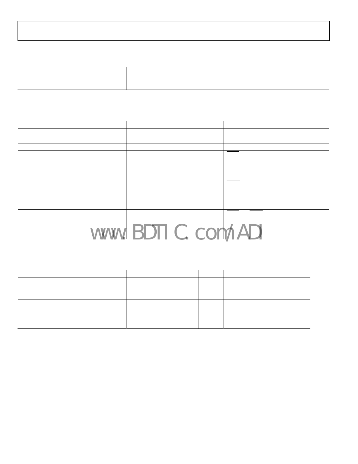
Table 2.
Parameter Min Typ Max Unit Test Conditions/Comments
INPUT IMPEDANCE 20 kΩ AINL/AINR
OUTPUT DC OFFSET VOLTAGE ±3 mV
POWER SUPPLIES
Table 3.
Parameter Min Typ Max Unit Test Conditions/Comments
ANALOG SUPPLY VOLTAGE (AVDD) 3.0 3.3 3.6 V
DIGITAL SUPPLY VOLTAGE (DVDD) 3.0 3.3 3.6 V
POWER TRANSISTOR SUPPLY VOLTAGE (PVDD) 9 15 18 V
POWER-DOWN CURRENT
AVDD 5 60 μA
DVDD 0.1 0.24 mA
PVDD 0.082 0.25 mA
MUTE CURRENT
AVDD 13 20 mA
DVDD 1.7 3.2 mA
PVDD 5.4 8 mA
OPERATING CURRENT
AVDD 13 30 mA
DVDD 2.7 4 mA
PVDD 44 65 mA
held low
STDN
held low
MUTE
and MUTE held high, no input
STDN
DIGITAL I/O
Table 4.
Parameter Min Typ Max Unit Test Conditions/Comments
INPUT VOLTAGE
Input Voltage High 2 V
Input Voltage Low 0.8 V
OUTPUT VOLTAGE
Output Voltage High 2 V @ 2 mA
Output Voltage Low 0.4 V @ 2 mA
LEAKAGE CURRENT ON DIGITAL INPUTS 10 μA
Rev. A | Page 4 of 24
ADAU1592
www.BDTIC.com/ADI
DIGITAL TIMING
Table 5.
Parameter Min Typ Unit Test Conditions/Comments
t
0.01
WAIT
t
650 ms Internal mute time
INT
t
10
HOLD
t
OUTx+/OUTx− SW
t
OUTx+/OUTx− MUTE
1
t
WAIT MIN
2
t
WAIT TYP
coupling capacitor value and the input resistance of the device. See the Power-Up/Power-Down Sequence section.
3
t
HOLD TYP
200 μs
200 μs
and t
is the recommended value for minimum pop and click during the unmute of the amplifier. The recommended value is 1 sec. It is calculated using the input
is the recommended value for minimum pop and click during the mute of the amplifier.
are the minimum times for fast turn-on and do not guarantee pop-and-click suppression.
HOLD MIN
1
1
1000
250
2
3
ms Wait time for unmute
μs Wait time for shutdown
Time delay after MUTE
Time delay after MUTE
held high until output starts switching
held low until output stops switching
STDN
INTERNAL MUTE
MUTE
OUTx+/OUTx–
NOTES
1. INTERNAL MUTE IS INTERNAL TO CHIP.
t
WAIT MIN
t
INT
t
HOLD M IN
06749-002
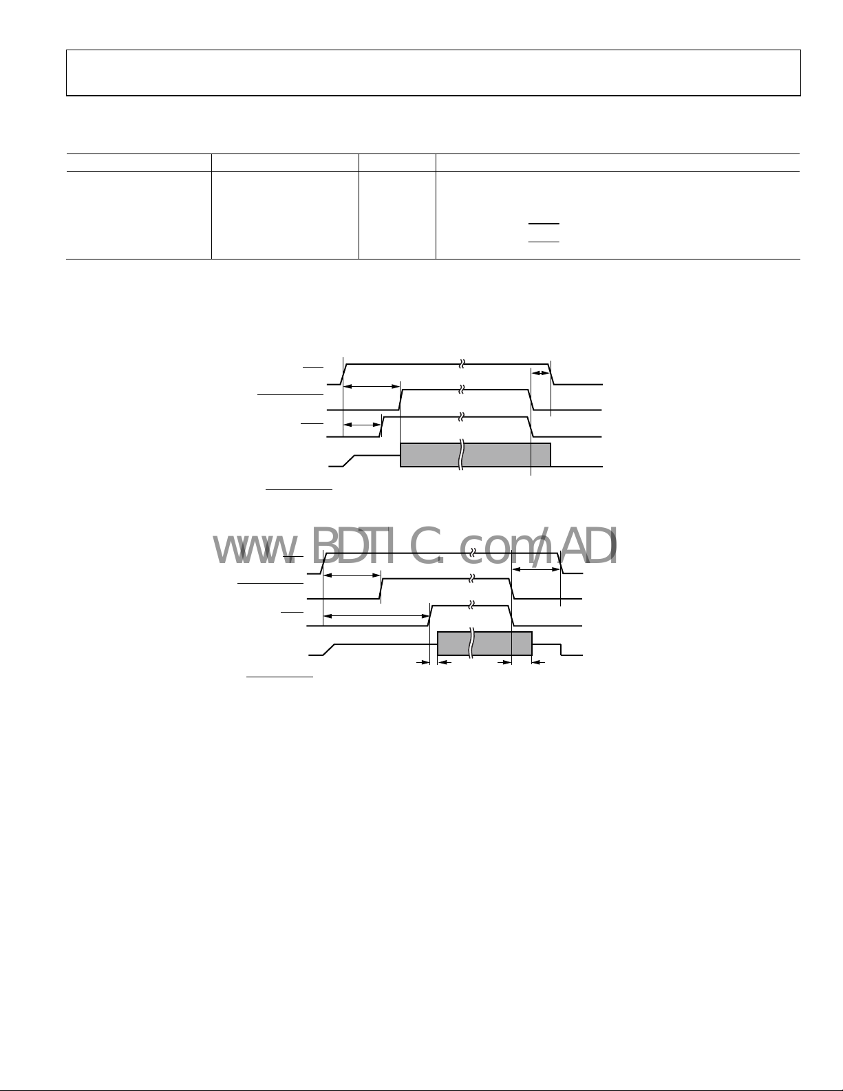
Figure 2. Timing Diagram (Minimum)
STDN
INTERNAL M UTE
MUTE
OUTx+/OUTx–
NOTES
1. INTERNAL MUTE IS INTERNAL TO CHIP.
t
INT
t
WAIT TYP
t
OUTx+/OUTx– SW
Figure 3. Timing Diagram (Typical)
t
HOLD TYP
t
OUTx+/OUTx– MUTE
06749-003
Rev. A | Page 5 of 24
ADAU1592
www.BDTIC.com/ADI
ABSOLUTE MAXIMUM RATINGS
Table 6.
Parameter Rating
DVDD to DGND −0.3 V to +3.6 V
AVDD to AGND −0.3 V to +3.6 V
PVDD to PGND1 −0.3 V to +20.0 V
MUTE/STDN Inputs
Operating Temperature Range −40°C to +85°C
Storage Temperature Range −65°C to +150°C
Maximum Junction Temperature 150°C
Lead Temperature
Soldering (10 sec) 260°C
Vapor Phase (60 sec) 215°C
Infrared (15 sec) 220°C
1
Includes any induced voltage due to inductive load.
DGND − 0.3 V to DVDD + 0.3 V
Stresses above those listed under Absolute Maximum Ratings
y cause permanent damage to the device. This is a stress
ma
rating only; functional operation of the device at these or any
other conditions above those indicated in the operational
section of this specification is not implied. Exposure to absolute
maximum rating conditions for extended periods may affect
device reliability.
THERMAL RESISTANCE
θJA is specified for the worst-case conditions, that is, a device
soldered in a circuit board for surface-mount packages.
Table 7. Thermal Resistance
Package Type θ
LFCSP-48 24.6 2.0 8.05 0.18 °C/W
TQFP-48 24.7 1.63 11 0.8 °C/W
1
With exposed pad (ePAD) soldered to 4-layer JEDEC standard PCB.
2
Through the bottom (ePAD) surface.
1
JA
1,2
θ
JC
ΨJB ΨJT Unit
ESD CAUTION
Rev. A | Page 6 of 24

ADAU1592
www.BDTIC.com/ADI
PIN CONFIGURATION AND FUNCTION DESCRIPTIONS
PGND
PGND
PVDD
PVDD
PVDD
PVDD
PVDD
PVDD
PVDD
PVDD
PGND
4847464544434241403938
PGND
37
OUTL–
1
OUTL–
2
OUTL–
3
OUTL+
4
OUTL+
5
OUTL+
6
TEST1
7
TEST0
8
9
ERR
OTW
10
MO/ST
11
TEST3
12
NOTES
1. EPAD NOT SHO WN AND INTERNALLY CONNECTED TO
PGND, DGND, AND AGND FOR TQ FP-48.
2. EPAD NOT SHO WN AND INTERNALLY CONNECTED TO
PGND AND DGND FOR LFCSP-48.
PIN 1
INDICATO R
ADAU1592
TOP VIEW
(Not to Scale)
1314151617181920212223
XTI
PGA1
PGA0
XTO
STDN
MUTE
DGND
DVDD
AVDD
AGND
VREF
OUTR–36
35
OUTR–
34
OUTR–
33
OUTR+
32
OUTR+
31
OUTR+
30
TEST13
29
TEST12
28
AINR
27
AINL
26
TEST9
25
TEST8
24
SLC_TH
06749-004
Figure 4. Pin Configuration
Table 8. Pin Function Descriptions
Pin Number Mnemonic Type
1
Description
1, 2, 3 OUTL− O Output of High Power Transistors, Left Channel Negative Polarity.
4, 5, 6 OUTL+ O Output of High Power Transistors, Left Channel Positive Polarity.
7 TEST1 I Reserved for Internal Use. Connect to DGND.
8 TEST0 I Reserved for Internal Use. Connect to DGND.
9
10
11
ERR
OTW
MO/ST
O Error Indicator (Active Low, Open-Drain Output).
O Overtemperature Warning Indicator (Active Low, Open-Drain Output).
I Mono/Stereo Mode Setting Pin for Stereo. Connect to DGND (for mono mode, connect to DVDD).
12 TEST3 I Reserved for Internal Use. Connect to DVDD.
13 PGA1 I Programmable Gain Amplifier Select, MSB.
14 PGA0 I Programmable Gain Amplifier Select, LSB.
15
16
MUTE
STDN
I Mute (Active Low Input).
I Shutdown/Reset Input (Active Low Input).
17 XTI I Quartz Crystal Connection/External Clock Input.
18 XTO O Quartz Crystal Connection/Clock Output.
19 DGND P Digital Ground for Digital Circuitry. Internally connected to exposed pad (ePAD).
20 DVDD P Positive Supply for Digital Circuitry.
21 AVDD P Positive Supply for Analog Circuitry. (Can be tied to DVDD.)
22 AGND P Analog Ground for Analog Circuitry. (See the notes in Figure 4 for connection to ePAD.)
23 VREF I AVDD/2 Voltage Reference Connection for External Filter.
24 SLC_TH I Slicer Threshold Adjust. (Connect to AGND via a resistor for slicer operation.)
25 TEST8 I Reserved for Internal Use. Connect to DGND.
26 TEST9 I Reserved for Internal Use. Connect to DGND.
27 AINL I Analog Input Left Channel.
28 AINR I Analog Input Right Channel.
29 TEST12 I Reserved for Internal Use. Connect to DGND.
30 TEST13 I Reserved for Internal Use. Connect to DGND.
31, 32, 33 OUTR+ O Output of High Power Transistors, Right Channel Positive Polarity.
Rev. A | Page 7 of 24

ADAU1592
www.BDTIC.com/ADI
Pin Number Mnemonic Type
34, 35, 36 OUTR− O Output of High Power Transistors, Right Channel Negative Polarity.
37, 38, 47, 48 PGND P Power Ground for High Power Transistors. Internally connected to ePAD.
39, 40, 41, 42,
43, 44, 45, 46
1
I = input, O = output, P = power.
PVDD P Positive Power Supply for High Power Transistors.
1
Description
Rev. A | Page 8 of 24
 Loading...