

www.BDTIC.com/ADI
Class-D Audio Power Amplifier
FEATURES
Integrated stereo modulator and power stage
0.005% THD + N
101 dB dynamic range
PSRR >55 dB
R
< 0.3 Ω (per transistor)
DS-ON
Efficiency > 90% (8 Ω)
EMI-optimized modulator
On/off-mute pop-noise suppression
Short-circuit protection
Overtemperature protection
APPLICATIONS
Flat panel televisions
PC audio systems
Mini-components
PGA0 PGA1
AINL
SLC_TH
AINR
AVD D
VREF
AGND
DVDD
DGND
PGA
SLICER
PGA
PGA0 PGA1
VOLTAGE
REFERENCE
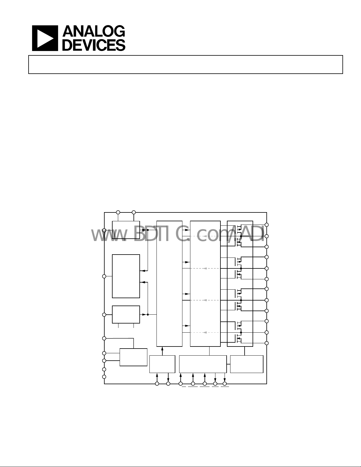
GENERAL DESCRIPTION
The ADAU1590 is a 2-channel, bridge-tied load (BTL)
switching audio power amplifier with an integrated Σ-
modulator.
The modulator accepts an analog input signal and generates
tching output to drive speakers directly. A digital,
a swi
microcontroller-compatible interface provides control of reset,
mute and PGA gain as well as output signals for thermal and
overcurrent error conditions. The output stage can operate
from supply voltages ranging from 9 V to 15 V. The analog
modulator and digital logic operate from a 3.3 V supply.
FUNCTIONAL BLOCK DIAGRAM
MODE CO NTROL
Figure 1.
LEVEL SHIFT
AND DEAD
TIME CONT ROL
LOGIC
OTWXTOXTI ERRMUTESTDN
Σ-Δ
MODULATOR
f
/2
CLK
CLOCK
OSCILLATOR
MO/ST
A1
A2
B1
B2
C1
C2
D1
D2
TEMPERATURE
OVERCURRENT
PROTECTION
ADAU1590
PVDD
OUTL+
PGND
PVDD
OUTL–
PGND
PVDD
OUTR+
PGND
PVDD
OUTR–
PGND
ADAU1590
06673-001
Rev. 0
Information furnished by Analog Devices is believed to be accurate and reliable. However, no
responsibility is assumed by Anal og Devices for its use, nor for any infringements of patents or ot her
rights of third parties that may result from its use. Specifications subject to change without notice. No
license is granted by implication or otherwise under any patent or patent rights of Analog Devices.
Trademarks and registered trademarks are the property of their respective owners.
One Technology Way, P.O. Box 9106, Norwood, MA 02062-9106, U.S.A.
Tel: 781.329.4700 www.analog.com
Fax: 781.461.3113 ©2007 Analog Devices, Inc. All rights reserved.

ADAU1590
www.BDTIC.com/ADI
TABLE OF CONTENTS
Features.............................................................................................. 1
Applications....................................................................................... 1
General Description ......................................................................... 1
Functional Block Diagram .............................................................. 1
Revision History ............................................................................... 2
Specifications..................................................................................... 3
Audio Performance ...................................................................... 3
DC Specifications ......................................................................... 4
Power Supplies .............................................................................. 4
Digital I/O ..................................................................................... 4
Digital Timing............................................................................... 5
Absolute Maximum Ratings............................................................ 6
Thermal Resistance ...................................................................... 6
ESD Caution.................................................................................. 6
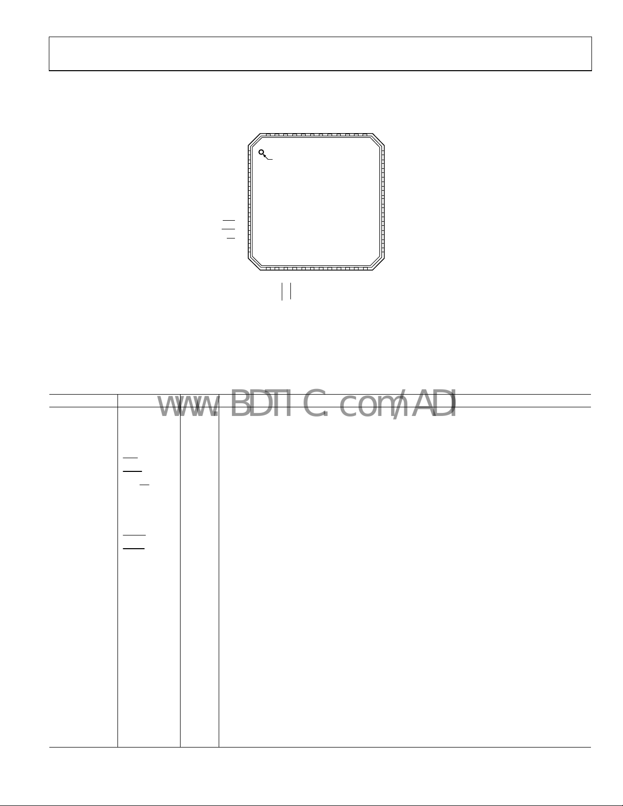
Pin Configuration and Function Descriptions............................. 7
Typical Performance Characteristics ............................................. 9
Theory of Operation ...................................................................... 15
Overview...................................................................................... 15
Modulator.................................................................................... 15
Slicer............................................................................................. 15
Power Stage ................................................................................. 16
Gain.............................................................................................. 16
Protection Circuits..................................................................... 16
Thermal Protection.................................................................... 16
Overcurrent Protection ............................................................. 16
Undervoltage Protection ........................................................... 17
Clock Loss Detection ................................................................. 17
Automatic Recovery from Protections.................................... 17
and
STDN
...................................................................... 17
REF
and C
............................................... 19
IN
MUTE
Power-Up/Power-Down Sequence .......................................... 18
DC Offset and Pop Noise.......................................................... 19
Selecting Value for C
Mono Mode................................................................................. 19
Power Supply Bypassing............................................................ 19
Clock ............................................................................................ 20
Applications Information.............................................................. 21
Outline Dimensions....................................................................... 23
Ordering Guide........................................................................... 23
REVISION HISTORY
5/07—Revision 0: Initial Version
Rev. 0 | Page 2 of 24
ADAU1590
www.BDTIC.com/ADI
SPECIFICATIONS
AVDD = DVDD = 3.3 V, PVDD = 12 V, ambient temperature = 25°C, load impedance = 6 , clock frequency = 24.576 MHz,
measurement bandwidth = 20 Hz to 20 kHz, unless otherwise noted.
AUDIO PERFORMANCE
Table 1.
Parameter Min Typ Max Unit Test Conditions/Comments
OUTPUT POWER
7 W 1% THD + N, 8 Ω
9 W 10% THD + N , 8 Ω
9 W 1% THD + N, 6 Ω
11.5 W 10% THD + N, 6 Ω
12.5 W 1% THD + N , 4 Ω
15.5 W 10% THD + N , 4 Ω
EFFICIENCY 87 % @ 12 W, 6 Ω
R
@ T
DS-ON
Per High-Side Transistor 0.28 Ω @ 100 mA
Per Low-Side Transistor 0.25 Ω @ 100 mA
THERMAL CHARACTERISTICS
Thermal Warning Active
Thermal Shutdown Active 150 °C Die temperature
OVERCURRENT SHUTDOWN ACTIVE 5 6 A Peak current
PVDD UNDERVOLTAGE SHUTDOWN 5.1 V
INPUT LEVEL FOR FULL-SCALE OUTPUT Full-scale output @ 1% THD + N
1.0 V
0.5 V
0.25 V
0.125 V
TOTAL HARMONIC DISTORTION + NOISE (THD+N) 0.005 % 1 kHz, P
SIGNAL-TO-NOISE RATIO (SNR) 99 101 dB A-weighted, referred to 1% THD + N output
DYNAMIC RANGE (DNR) 99 101 dB A-weighted, measured with −60 dBFS input
CROSSTALK (LEFT TO RIGHT OR RIGHT TO LEFT) −90 dB @ full-scale output voltage, 1% THD + N, 1 kHz
AMPLIFIER GAIN PVDD = 12 V, 6 Ω
PGA = 0 dB 17 dB
PGA = 6 dB 23 dB
PGA = 12 dB 29 dB
PGA = 18 dB 35 dB
OUTPUT NOISE VOLTAGE PVDD = 12 V, 6 Ω
PGA = 0 dB 65 μV
PGA = 6 dB 83 μV
PGA = 12 dB 130 μV
PGA = 18 dB 230 μV
POWER SUPPLY REJECTION RATIO (PSRR) 57 dB
1
Output powers above 12 W at 4 Ω and above 18 W at 6 Ω are not continuous and are thermally limited by the package dissipation.
2
Thermal warning flag is for indication of device TJ reaching close to shutdown temperature.
1
2
1 kHz
= 25°C
CASE
135 °C Die temperature
PGA gain = 0 dB
RMS
PGA gain = 6 dB
RMS
PGA gain = 12 dB
RMS
PGA gain = 18 dB
RMS
= 1 W, PGA gain = 0 dB
OUT
20 Hz to 20 kHz, 1.2 V p-p ripple, inputs ac-
upled to AGND
co
Rev. 0 | Page 3 of 24
ADAU1590
www.BDTIC.com/ADI
DC SPECIFICATIONS
Table 2.
Parameter Min Typ Max Unit Test Conditions/Comments
INPUT IMPEDANCE 20 kΩ AINL/AINR
OUTPUT DC OFFSET VOLTAGE ±3 mV
POWER SUPPLIES
Table 3.
Parameter Min Typ Max Unit Test Conditions/Comments
ANALOG SUPPLY VOLTAGE (AVDD) 3.0 3.3 3.6 V
DIGITAL SUPPLY VOLTAGE (DVDD) 3.0 3.3 3.6 V
POWER TRANSISTOR SUPPLY VOLTAGE (PVDD) 9 12 15 V
POWER-DOWN CURRENT
AVDD 6 60 μA
DVDD 0.14 0.24 mA
PVDD 0.06 0.25 mA
MUTE CURRENT
AVDD 13 20 mA
DVDD 1.8 3.2 mA
PVDD 4.5 8 mA
OPERATING CURRENT
AVDD 13 30 mA
DVDD 2.7 4 mA
PVDD 34 65 mA
held low
STDN
held low
MUTE
and MUTE held high, no input
STDN
DIGITAL I/O
Table 4.
Parameter Min Typ Max Unit Test Conditions/Comments
INPUT VOLTAGE
Input Voltage High 2 V
Input Voltage Low 0.8 V
OUTPUT VOLTAGE
Output Voltage High 2 V @ 2 mA
Output Voltage Low 0.4 V @ 2 mA
LEAKAGE CURRENT ON DIGITAL INPUTS 10 μA
Rev. 0 | Page 4 of 24
ADAU1590
www.BDTIC.com/ADI
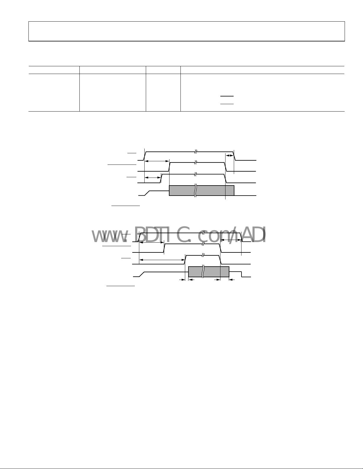
DIGITAL TIMING
Table 5.
Parameter Min Typ Unit Test Conditions/Comments
t
0.01
WAIT
t
650 ms Internal mute time
INT
t
10
HOLD
t
OUTx+/OUTx− SW
t
OUTx+/OUTx− MUTE
1
t
WAIT MIN
2
t
WAIT TYP
coupling capacitor value and the input resistance of the device. See the Power-Up/Power-Down Sequence section.
3
t
HOLD TYP
200 μs
200 μs
and t
is the recommended value for minimum pop and click during the unmute of the amplifier. The recommended value is 1 sec. It is calculated using the input
is the recommended value for minimum pop and click during the mute of the amplifier.
are the minimum times for fast turn-on and do not guarantee pop-and-click suppression.
HOLD MIN
1
1
1000
250
2
3
ms Wait time for unmute
μs Wait time for shutdown
Time delay after MUTE
Time delay after MUTE
held high until output starts switching
held low until output stops switching
STDN
INTERNAL M UTE
MUTE
OUTx+/OUTx–
NOTES
1. INTERNAL MUTE IS I NTERNAL TO CHIP.
t
WAIT MIN
t
INT
t
HOLD M IN
06673-002
Figure 2.Timing Diagram (Minimum)
STDN
INTERNAL MUTE
MUTE
OUTx+/OUTx–
NOTES
1. INTERNAL MUTE IS I NTERNAL TO CHIP.
t
INT
t
WAIT TYP
t
OUTx+/OUTx– SW
Figure 3. Timing Diagram (Typical)
t
HOLD TYP
t
OUTx+/OUTx– MUTE
06673-003
Rev. 0 | Page 5 of 24
ADAU1590
www.BDTIC.com/ADI
ABSOLUTE MAXIMUM RATINGS
Table 6.
Parameter Rating
DVDD to DGND −0.3 V to +3.6 V
AVDD to AGND −0.3 V to +3.6 V
PVDD to PGND1 −0.3 V to +20.0 V
MUTE/STDN Inputs
Operating Temperature Range −40°C to +85°C
Storage Temperature Range −65°C to +150°C
Maximum Junction
Temperature
Lead Temperature
Soldering (10 sec) 260°C
Vapor Phase (60 sec) 215°C
Infrared (15 sec) 220°C
1
Includes any induced voltage due to inductive load.
DGND − 0.3 V to DVDD + 0.3 V
150°C
Stresses above those listed under Absolute Maximum Ratings
may cause permanent damage to the device. This is a stress
rating only; functional operation of the device at these or any
other conditions above those indicated in the operational
section of this specification is not implied. Exposure to absolute
maximum rating conditions for extended periods may affect
device reliability.
THERMAL RESISTANCE
θJA is specified for the worst-case conditions, that is, a device
soldered in a circuit board for surface-mount packages.
Table 7. Thermal Resistance
Package Type θ
LFCSP-48 24.6 2.0 8.05 0.18 °C/W
TQFP-48 24.7 1.63 11 0.8 °C/W
1
With exposed pad (ePAD) soldered to 4-layer JEDEC standard PCB.
2
Through the bottom (ePAD) surface.
1
JA
1, 2
θ
ΨJB ΨJT Unit
JC
ESD CAUTION
Rev. 0 | Page 6 of 24
ADAU1590
www.BDTIC.com/ADI
PIN CONFIGURATION AND FUNCTION DESCRIPTIONS
PGND
PGND
PVDD
PVDD
PVDD
PVDD
PVDD
PVDD
PVDD
PVDD
PGND
4847464544434241403938
PGND
37
OUTL–
1
OUTL–
2
OUTL–
3
OUTL+
4
OUTL+
5
OUTL+
6
TEST1
7
TEST0
8
9
ERR
OTW
10
MO/ST
11
TEST3
12
NOTES
1. EPAD NOT SHO WN AND INTERNALLY CONNECTED TO
PGND, DGND, AND AGND FOR TQ FP-48.
2. EPAD NOT SHO WN AND INTERNALLY CONNECTED TO
PGND AND DGND FOR LFCSP-48.
PIN 1
INDICATO R
ADAU1590
TOP VIEW
(Not to Scale)
1314151617181920212223
XTI
PGA1
PGA0
XTO
STDN
MUTE
DGND
DVDD
AVDD
AGND
VREF
OUTR–36
35
OUTR–
34
OUTR–
33
OUTR+
32
OUTR+
31
OUTR+
30
TEST13
29
TEST12
28
AINR
27
AINL
26
TEST9
25
TEST8
24
SLC_TH
06673-004
Figure 4. Pin Configuration
Table 8. Pin Function Descriptions
Pin. Number Mnemonic Type1Description
1, 2, 3 OUTL− O Output of High Power Transistors, Left Channel Negative Polarity.
4, 5, 6 OUTL+ O Output of High Power Transistors, Left Channel Positive Polarity.
7 TEST1 I Reserved for Internal Use. Connect to DGND.
8 TEST0 I Reserved for Internal Use. Connect to DGND.
9
10
11
ERR
OTW
MO/ST
O Error Indicator (Active Low, Open-Drain Output).
O Overtemperature Warning Indicator (Active Low Open-Drain Output).
I Mono/Stereo Mode Setting Pin for Stereo. Connect to DGND (for mono mode, connect to DVDD).
12 TEST3 I Reserved for Internal Use. Connect to DVDD.
13 PGA1 I Programmable Gain Amplifier Select, MSB.
14 PGA0 I Programmable Gain Amplifier Select, LSB.
15
16
MUTE
STDN
I Mute (Active Low Input).
I Shutdown/Reset Input (Active Low Input).
17 XTI I Quartz Crystal Connection/External Clock Input.
18 XTO O Quartz Crystal Connection/Clock Output.
19 DGND P Digital Ground for Digital Circuitry. Internally connected to exposed pad (ePAD).
20 DVDD P Positive Supply for Digital Circuitry.
21 AVDD P Positive Supply for Analog Circuitry. (Can be tied to DVDD.)
22 AGND P Analog Ground for Analog Circuitry. (See the notes in Figure 4 for connection to ePAD.)
23 VREF I AVDD/2 Voltage Reference Connection for External Filter.
24 SLC_TH I Slicer Threshold Adjust. (Connect to AGND via a resistor for slicer operation.)
25 TEST8 I Reserved for Internal Use. Connect to DGND.
26 TEST9 I Reserved for Internal Use. Connect to DGND.
27 AINL I Analog Input Left Channel.
28 AINR I Analog Input Right Channel.
29 TEST12 I Reserved for Internal Use. Connect to DGND.
30 TEST13 I Reserved for Internal Use. Connect to DGND.
31, 32, 33 OUTR+ O Output of High Power Transistors, Right Channel Positive Polarity.
Rev. 0 | Page 7 of 24

ADAU1590
www.BDTIC.com/ADI
Pin. Number Mnemonic Type1Description
34, 35, 36 OUTR− O Output of High Power Transistors, Right Channel Negative Polarity.
37, 38, 47, 48 PGND P Power Ground for High Power Transistors. Internally connected to EPAD.
39, 40, 41, 42,
43, 44, 45, 46
1
I = input, O = output, P = power.
PVDD P Positive Power Supply for High Power Transistors.
Rev. 0 | Page 8 of 24

ADAU1590
–
–
–
–
–
–
www.BDTIC.com/ADI
TYPICAL PERFORMANCE CHARACTERISTICS
20
–30
–40
–50
–60
THD + N
–70
–80
–90
THD OR THD + N (d B)
–100
–110
–120
THD
10m 10100m 1
OUTPUT PO WER (W)
Figure 5. THD or THD + N vs. Output Power, 4 Ω, PVDD = 9 V
6673-005
20
–30
–40
–50
–60
THD OR THD + N (d B)
–100
–110
–120
–70
–80
–90
THD + N
THD
10m 10100m 1
OUTPUT PO WER (W)
Figure 8. THD or THD + N vs. Output Power, 4 Ω, PVDD = 12 V
06673-008
20
–30
–40
–50
–60
–70
THD + N
–80
–90
THD OR THD + N (d B)
–100
–110
–120
THD
10m 10100m 1
OUTPUT PO WER (W)
Figure 6. THD or THD + N vs. Output Power, 6 Ω, PVDD = 9 V
20
–30
–40
–50
–60
–70
THD + N
–80
–90
THD OR THD + N (d B)
–100
–110
–120
THD
10m 10100m 1
OUTPUT PO WER (W)
Figure 7. THD or THD + N vs. Output Power, 8 Ω, PVDD = 9 V
20
–30
–40
–50
–60
THD + N
–70
–80
–90
THD OR THD + N (d B)
–100
–110
–120
6673-006
THD
10m 10100m 1
OUTPUT PO WER (W)
6673-009
Figure 9. THD or THD + N vs. Output Power, 6 Ω, PVDD = 12 V
20
–30
–40
–50
–60
THD + N
–70
–80
–90
THD OR THD + N (d B)
–100
–110
–120
06673-007
THD
10m 10100m 1
OUTPUT PO WER (W)
06673-010
Figure 10. THD or THD + N vs. Output Power, 8 Ω, PVDD = 12 V
Rev. 0 | Page 9 of 24

ADAU1590
www.BDTIC.com/ADI
25
POWER LI MITED DUE T O PACKAGE DIS SIPATIO N
20
4Ω
15
6Ω
10
OUTPUT PO WER (W)
5
0
91
PVDD (V)
Figure 11. Output Power v
s. PVDD @ 0.1% THD + N
8Ω
510 11 12 13 14
6673-011
OUTPUT (dBr)
–10
–20
–30
–40
–50
–60
–70
–80
–90
–100
–110
–120
–130
–140
–15
–160
0
0
0
2204 6 8 10 12 14 16 18
FREQUENCY (kHz)
0dBr = 9.5W
Figure 14. FFT @ 1W, 6 Ω, PVDD = 12 V, PGA = 0 dB, 1 kHz Sine
06673-014
25
POWER LIMITED DUE T O PACKAGE DISSIPATIO N
20
15
10
OUTPUT POWER (W)
5
0
91
PVDD (V)
4Ω
6Ω
8Ω
510 11 12 13 14
06673-012
Figure 12. Output Power vs. PVDD @ 1% THD + N
30
25
20
15
10
OUTPUT PO WER (W)
5
0
91510 11 12 13 14
POWER LI MITED DUE T O PACKAGE DISSIPATIO N
PVDD (V)
4Ω
6Ω
8Ω
06673-013
0
–10
–20
–30
–40
–50
–60
–70
–80
–90
–100
OUTPUT (dBr)
–110
–120
–130
–140
–150
–160
0
2204 6 8 10 12 14 16 18
Figure 15. FFT @ −60 dBFS, 6 Ω, PVDD = 12 V, PGA = 0 dB, 1 kHz Sine
0
–10
–20
–30
–40
–50
–60
–70
–80
OUTPUT (d BV)
–90
–100
–110
–120
0
–13
–140
0
2204 6 8 10 12 14 16 18
FREQUENCY (kHz)
FREQUENCY (kHz)
0dBr = 9.5W
06673-015
06673-016
Figure 13. Output Power vs. PVDD @ 10% THD + N
Rev. 0 | Page 10 of 24
Figure 16. FFT No Input, 6 Ω, PVDD = 12 V, PGA = 0 dB

ADAU1590
www.BDTIC.com/ADI
0
–10
–20
–30
–40
–50
–60
–70
–80
THD OR THD + N (d B)
–90
–100
–110
–120
20 10k100 1k
THD + N
THD
FREQUENCY (Hz)
Figure 20. THD or THD + N vs. Frequency @ 1 W, 4 Ω, PVDD = 12 V, PGA = 0 dB
6673-020
OUTPUT (dBr)
–10
–20
–30
–40
–50
–60
–70
–80
–90
–100
–110
–120
–130
–140
–150
–160
0
0
22
6 8 1012141618
FREQUENCY (kHz)
0dBr = 9.5W
2204
06673-017
Figure 17. FFT @ 1 W, 6 Ω, PVDD = 12 V, PGA = 0 dB, 19 kHz and 20 kHz Sine
0
–10
–20
–30
–40
–50
OUTPUT (dB)
–100
–110
–120
–60
–70
–80
–90
20
100 1k 10k
FREQUENCY (Hz)
RIGHT TO LEFT
LEFT TO RIGHT
Figure 18. Crosstalk @ 1 W, 6 Ω, PVDD = 12 V, PGA = 0 dB
0
–10
–20
–30
–40
–50
OUTPUT (d B)
–100
–110
–120
–60
–70
–80
–90
20
100 1k 10k
FREQUENCY (Hz)
RIGHT TO LEFT
LEFT TO RIGHT
Figure 19. Crosstalk @ Full Scale, 6 Ω, PVDD = 12 V, PGA = 0 dB
0
–10
–20
–30
–40
–50
–60
–70
–80
THD OR THD + N (d B)
–90
–100
–110
–120
20 10k100 1k
06673-018
THD + N
THD
FREQUENCY (Hz)
6673-021
Figure 21. THD or THD + N vs. Frequency @ 1 W, 6 Ω, PVDD = 12 V, PGA = 0 dB
0
–10
–20
–30
–40
–50
–60
–70
–80
THD OR THD + N (d B)
–90
–100
–110
–120
20 10k100 1k
06673-019
THD + N
THD
FREQUENCY (Hz)
6673-022
Figure 22. THD or THD + N vs. Frequency @ 1 W, 8 Ω, PVDD = 12 V, PGA = 0 dB
Rev. 0 | Page 11 of 24

ADAU1590
www.BDTIC.com/ADI
2.0
1.8
1.6
1.4
1.2
1.0
0.8
0.6
0.4
0.2
0
–0.2
–0.4
OUTPUT (dBr)
–0.6
–0.8
–1.0
–1.2
–1.4
–1.6
–1.8
–2.0
20 1 00 1k 10k
FREQUENCY (Hz)
Figure 23. Frequency Response @ 1 W, 6 Ω, PVDD = 12 V, PGA = 0 dB
37
35
33
31
29
27
25
GAIN (dB)
23
21
19
17
15
20 1 00 1k 10k
FREQUENCY (Hz)
PGA 18dB
PGA 12dB
PGA 6dB
PGA 0dB
Figure 24. Gain vs. Frequency @ 1 W, 6 Ω, PVDD = 12 V, 6 Ω
90
80
70
60
50
40
EFFICIENCY (%)
30
20
10
0
0 4 6 8 10 12 14 16 18
06673-023
POWER LI MITED DUE T O PACKAGE DISSIPATIO N
2
OUTPUT POWER (W)
06673-026
Figure 26. Efficiency vs. Output Power, 12 V, 4 Ω
100
90
80
70
60
50
40
EFFICIENCY (%)
30
20
10
0
06673-024
2
0 4 6 8 10 12 14
OUTPUT PO WER (W)
06673-027
Figure 27. Efficiency vs. Output Power,12 V, 6 Ω
0
–10
–20
–30
–40
–50
PSRR (dB)
–60
–70
–80
–90
–100
20 1 00 1k 10k
FREQUENCY (Hz)
Figure 25. PSRR vs. Frequency, N
o Input Signal
Ripple = 1.2 V p-p, PVDD = 12 V, 6 Ω
6673-025
Rev. 0 | Page 12 of 24
100
90
80
70
60
50
40
EFFICIENCY (%)
30
20
10
0
2
0 4 6 8 10 12
OUTPUT PO WER (W)
Figure 28. Efficiency vs. Output Power, 12 V, 8 Ω
06673-028

ADAU1590
www.BDTIC.com/ADI
10
POWER LI MITED DUE T O PACKAGE DIS SIPATIO N
9
8
7
6
5
DISS
P
4
3
2
1
0
0 10152
Figure 29. Power Dissipatio
5
P
PER CHANNEL STEREO MODE
OUT
n vs. Output Power, 12 V, 4 Ω, Stereo Mode,
Both Channels Driven
0
06673-029
6
5
4
3
MAX (W)
DISS
P
2
1
0
0 10 20 30 40 50 60 70 80 90 100 110 120 130 140 150 160
T
(°C)
AMBIENT
Figure 32. Power Dissipation Derating vs. Ambient Temperature
06673-032
4
3
2
DISS
P
1
0
010
Figure 30. Power Dissipatio
5
P
PER CHANNEL STEREO MODE
OUT
n vs. Output Power, 12 V, 6 Ω, Stereo Mode,
15
Both Channels Driven
3
2
DISS
P
1
40
35
30
25
20
15
OUTPUT PO WER (W)
10
5
0
9 101112131415
06673-030
PVDD (V)
3Ω
4Ω
6Ω
8Ω
6673-033
Figure 33. Output Power vs. PVDD, Mono Mode, THD + N, 20 dB
30
25
20
15
10
OUTPUT POWER (W)
3Ω
4Ω
6Ω
8Ω
0
01011567894321 12
P
PER CHANNEL STEREO MODE
OUT
Figure 31. Power Dissipatio
n vs. Output Power, 12 V, 8 Ω, Stereo Mode,
06673-031
Both Channels Driven
Rev. 0 | Page 13 of 24
5
0
9 101112131415
PVDD (V)
Figure 34. Output Power vs. PVDD, Mono Mode, THD + N, 40 dB
6673-034

ADAU1590
www.BDTIC.com/ADI
25
20
3Ω
15
10
OUTPUT POWER (W)
5
0
9 101112131415
PVDD (V)
4Ω
6Ω
8Ω
Figure 35. Output Power vs. PVDD, Mono Mode, THD + N, 60 dB
90
80
70
60
50
40
EFFICIENCY (%)
30
20
10
0
0246810121416182022242628
OUTPUT PO WER (W)
Figure 36. Efficiency vs. Output Power, Mono Mode, 12 V, 3 Ω
06673-035
06673-036
100
90
80
70
60
50
40
EFFICIENCY (%)
30
20
10
0
0 2 4 6 8 101214161820
OUTPUT POWER (W)
Figure 37. Efficiency vs. Output Power, Mono Mode, 12 V, 4 Ω
06673-037
Rev. 0 | Page 14 of 24

ADAU1590
www.BDTIC.com/ADI
THEORY OF OPERATION
OVERVIEW
The ADAU1590 is a 2-channel high performance switching
audio power amplifier. Each of the two Σ- modulators converts
a single-ended analog input into a 2-level PDM output. This
PDM pulse stream is output from the internal full differential
power stage. The ADAU1590 has built-in circuits to suppress the
turn-on and turn off pop and click. The ADAU1590 also offers
extensive thermal and overcurrent protection circuits.
MODULATOR
The modulator is a 5th-order Σ- with feedback from the power
stage connected internally. This helps reduce the external
connections. The 5
th
-order modulator switches to a lower order
near full-scale inputs. The modulator gain is optimized at 19 dB
for 15 V operation. The Σ- modulator outputs a pulse density
modulation (PDM) 1-bit stream, which does not produce
distinct sharp peaks and harmonics in the AM band like
conventional fixed-frequency PWM.
The Σ- modulators require feedback to generate PDM stream
w
ith respect to the input. The feedback for the modulators
comes from the power stage. This helps reduce the nonlinearity
in the power stages and achieve excellent THD + N performance. The feedback also helps in achieving good PSRR. In the
ADAU1590, the feedback from the power stage is internally
connected. This helps reduce the external connections for ease
in PCB layout.
The Σ- modulators operate in a discrete time domain and
N
yquist frequency limit, which is half the sampling frequency.
The modulator uses the master clock of 12.288 MHz. This is
generated by dividing the external clock input by 2. This sets
the f
/2 around 6.144 MHz. This is sufficient for the audio
S
bandwidth of 22 kHz. The modulator shapes the quantization
noise and transfers it outside the audio band. The noise floor
rises sharply above 20 kHz. This ensures very good signal-tonoise ratio (SNR) in the audio band of 20 kHz. The 6.144 MHz
bandwidth allows the modulator order to be set around the 5
th
order. The modulator uses proprietary dynamic hysteresis to
reduce the switching rate or frequency to around 700 kHz.
This reduces the switching losses and achieves good efficiency.
The dynamic hysteresis helps the modulator to continuously
track the change in PVDD and the input level to keep the
modulator stable.
SLICER
The ADAU1590 has a built-in slicer block following the PGA
and before the modulator. The slicer block is essentially a hard
limiter included for limiting the input signal to the modulator.
This, in turn, limits the output power at a given supply voltage.
The slicer in the ADAU1590 is normally inactive at lower input
levels but is activated as soon as the peak input voltage exceeds
the set threshold. The threshold can be set externally by
connecting a resistor from SLC_TH (Pin 24) to ground. This
feature allows the user to adjust the slicer to the desired value
and to limit the output power. For input signals higher than the
set threshold, the slicer clips the input signal to the modulator.
This adds distortion due to clipping of the signal input to the
modulator. This is especially helpful in applications where the
output power available needs to be reduced instead of reducing
the supply voltage.
Figure 38 is a plot showing THD + N vs. the input level at
0 dB PGA, 12
V, and 6 , and demonstrates the difference
between a device with and without the slicer.
0
–5
–10
–15
–20
–25
–30
–35
–40
–45
–50
–55
–60
THD + N (dB)
–65
–70
–75
–80
–85
–90
–95
–100
0.1 1.20.2 0.3 0.4 0.5 0.6 0.7 0.8 0.9 1.0 1.1
Figure 38. THD + N vs. Input Level @ PGA = 0 dB, 12 V
SLICER 1.1V
SLICER 1.17V
SLICER 1.24V
SLICER 1.32V
SLICER DISABLED
INPUT (V rms)
06673-038
Figure 39 depicts the typical output power vs. input at different
slicer settings.
12.0
11.5
11.0
10.5
10.0
9.5
9.0
8.5
8.0
7.5
7.0
6.5
6.0
5.5
5.0
4.5
4.0
OUTPUT PO WER (W)
3.5
3.0
2.5
2.0
1.5
1.0
0.5
0
0.1 1.20.2 0.3 0.4 0.5 0.6 0.7 0.8 0.9 1.0 1.1
Figure 39. Typical Output Power vs. Input, a
SLICER DISABLED
INPUT (V rms)
SLICER 1. 32V
SLICER 1. 24V
SLICER 1. 17V
SLICER 1. 10V
t Different Slicer Settings
6673-039
From Figure 39, it can be seen that the slicer effectively reduces
the output power depending on its setting.
Internally, the slicer block receives the input from the PGA.
Figure 40 shows the block for slicer threshold adjust, SLC_TH
(P
in 24).
Rev. 0 | Page 15 of 24

ADAU1590
www.BDTIC.com/ADI
V
CM
50kΩ
SLICER_LEVEL
Figure 40. Block for Slicer Threshold Adjust, SLC_TH
V
TH
R
EXTERNAL
PIN 24 (SLC_T H)
06673-040
The slicer threshold can be set externally using a resistor as
follows:
V
= (AVDD/2) × (50 k/50 k + R
TH
EXTERNAL
)
where:
AV
D D = 3.3 V typical.
V
is the voltage threshold at which the slicer is activated.
TH
The following equation can be used to calculate the input signal
a
t which the slicer becomes active:
V
TH
V
=
IN RMS
Therefore, for AV
R
EXTERNAL
V
IN RMS
D D = 3.3 V typical and V
= 24.9 k
= 0.864 V
Thus, the slicer is activated at and above 0.864 V
0.91.414 ×
= 1.1 V,
TH
.
IN RMS
This feature allows the user to set the slicer and, in turn, reduces
he output power at a given supply voltage.To disable the slicer,
t
SLC_TH should be connected to AGND.
ical values for R
typ
Table 9. Typical R
VTH (V) R
1.1 24.9 0.864
1.17 20.5 0.919
1.24 16.5 0.974
1.32 12.4 1.037
.
EXTERNAL
Values
EXTERNAL
(kΩ) V
EXTERNAL
Tabl e 9 shows the
(V)
IN RMS
POWER STAGE
The ADAU1590 power stage comprises a high-side PMOS and
a low-side NMOS. The typical R
NMOS stage does not need an external bootstrap capacitor and
simplifies the high-side driver design. The power stage also has
comprehensive protection circuits to detect the faults in typical
applications. See the
Protection Circuits section for further details.
is ~300 m. The PMOS-
DS-ON
GAIN
The gain of the amplifier is set internally using feedback resistors optimized for 12 V nominal operation. The typical gain
values are tabulated in Tabl e 1. The typical gain is 17 dB with
PGA s
et to 0 dB. PGA0 (Pin 14) and PGA1 (Pin 13) are used
for setting the desired gain.
The gain can be set according to Tabl e 10 . Note that the amplif
ier full-scale input level changes as per the PGA gain setting.
Table 10. Gain Settings
Full-Scale
PGA1
(Pin 13)
0 0 0 17 1
0 1 6 23 0.5
1 0 12 29
1 1 18 35 0.125
PGA0
(Pin14)
PGA
Gain (dB)
Amplifier
Gain (dB)
Input L
evel
(V
)
RMS
0.25
PROTECTION CIRCUITS
The ADAU1590 includes comprehensive protection circuits. It
includes thermal warning, thermal overheat, and overcurrent or
short-circuit protection on the outputs. The
ERR
and
OTW
outputs are open drain and require external pull-up resistors.
The outputs are capable of sinking 10 mA. The open-drain
outputs are useful in multichannel applications where more
than one ADAU1590 is used. The error outputs of multiple
ADAU1590s can be OR’ed to simplify the system design.
The logic outputs of the error flags ease the system design of
using a microcontroller.
THERMAL PROTECTION
Thermal protection in the ADAU1590 is categorized into two
error flags: one as thermal warning and the other as thermal
shutdown. When the device junction temperature reaches near
135°C (±5°C), the ADAU1590 outputs a thermal warning error
flag by pulling
OTW
(Pin 10) low. This flag can be used by the
microcontroller in the system for indication to the user or can
be used to lower the input level to the amplifier to prevent
thermal shutdown. The device continues operation until
shutdown temperature is reached.
When the device junction temperature exceeds 150°C, the
de
vice outputs an error flag by pulling
error flag is latched. To restore the operation,
ERR
(Pin 9) low. This
MUTE
(Pin 15)
needs to be toggled to low and then to high again.
OVERCURRENT PROTECTION
The overcurrent protection in the ADAU1590 is set internally at
a 5 A peak output current. The device protects the output
devices against excessive output current by pulling
low. This error flag is latched. To restore the normal operation,
(Pin 15) needs to be toggled to low and then to high
MUTE
again. The error flag is useful for the microcontroller in the
system to indicate abnormal operation and to initiate the audio
sequence. The device senses the short-circuit condition
MUTE
ERR
(Pin 9)
Rev. 0 | Page 16 of 24

ADAU1590
A
www.BDTIC.com/ADI
on the outputs after the LC filter. Typical short-circuit conditions include shorting of the output load, and shorting to either
PVDD or PGND.
UNDERVOLTAGE PROTECTION
The ADAU1590 is also comprised of an undervoltage protection circuit, which senses the undervoltage on PVDD. When
the PVDD supply goes below the operating threshold, the
output FETs are turned to a high-Z condition. In addition, the
device issues an error flag by pulling
is latched. To restore the operation,
ERR
low. This condition
(Pin 15) needs to
MUTE
be toggled to low and then to high again.
CLOCK LOSS DETECTION
The ADAU1590 includes a clock loss detection circuit. In case
the master clock to the part is lost, the
condition is latched. To restore operation,
ERR
flag is set. This
MUTE
needs to be
toggled low and high again.
AUTOMATIC RECOVERY FROM PROTECTIONS
In certain applications, it is desired for the amplifier to recover
itself from thermal protection without the need for system
microcontroller intervention.
The ADAU1590 thermal protection circuit issues two error
MUTE
TO MUTE
LOGIC INPUT
OTW
) and the
as shown in
06673-041
MUTE
pin.
OTW
signal
Rev. 0 | Page 17 of 24
nals for this purpose: one a thermal warning (
sig
other a thermal shutdown (
ERR
).
With the two error signals, there are two options available for
usi
ng the protections:
• Op
• Op
tion 1: Using
tion 2: Using
OTW
ERR
The following sections provide further details of these two options.
Option 1: Using
OTW
The
OTW
pin is pulled low when the die temperature reaches
130°C to 135°C. This pin can be wired to
Figure 41, using an RC circuit.
10
15
DVDD
R1
100kΩ
C1
47µF
OTW
also pulls down the
D1
1N4148
ADAU1590
OTW
MUTE
Figure 41. Option 1 Schematic for Autorecovery
The low logic level on
The bridge is shut down and starts cooling or the die temperature
starts reducing. When it reaches around 120°C, the
starts going high. While this pin is tied to a capacitor with a
resistor pulled to DVDD, the voltage on this pin starts rising
slowly towards DVDD. When it reaches the CMOS threshold,
MUTE
is deasserted and the amplifier starts functioning again.
This cycle repeats itself depending on the input signal
conditions and the temperature of the die. This option allows
device operation that is safely below the shutdown temperature
of 150°C and allows the amplifier to recover itself without the
need for microcontroller intervention.
Option 2: Using
Option 2 is similar to Option 1 except the
MUTE
instead of
DAU1590
ERR
ERR
pin is tied to
OTW
. See the circuit in Figure 42.
DVDD
R1
100kΩ
D1
C1
47µF
1N4148
TO MUTE
LOGIC INPUT
9
ERR
15
MUTE
Figure 42. Option 2 Schematic for Autorecovery
06673-042
In this case, the part goes into shutdown mode due to any of the
error generating events like output overcurrent, overtemperature, missing PVDD or DVDD, or clock loss. The part recovers
itself based on the same circuit operation in Figure 41.
However, if the part goes into error mode due to overtemperat
ure, then the device would have reached its maximum limit of
150°C (15°C to 20°C higher than Option 1). If it goes into error
mode due to an overcurrent from a short circuit on the speaker
outputs, then the part keeps itself recycling on and off until the
short circuit is removed.
It is possible that, with this operation, the part is subjected to a
m
uch higher temperature and current stress continuously. This,
in turn, reduces the part’s reliability in the long term. Therefore,
using Option 1 for autorecovery from thermal protection and
using the system microcontroller to indicate to the user of an
error condition is recommended.
MUTE AND STDN
MUTE
The
used to control the turn-on/turn-off for ADAU1590.
STDN
The
and the device is in its energy saving mode. The modulator is
inactive and the power stage is in high-Z state. The high logic
level input on the
modulator is running internally but the power stage is still in
high-Z state.
When the
active with a soft turn-on to avoid the pop and clicks. The low
level on the
recommended to be used to mute the audio output. See the
Power-Up/Power-Down Sequence section for more details.
STDN
and
input is active low when the
MUTE
MUTE
pins are 3.3 V logic-compatible inputs
STDN
STDN
pin wakes up the device. The
pin is pulled high, the power stage becomes
pin disables the power stage and is
pin is pulled low

ADAU1590
t
t
A
S
A
www.BDTIC.com/ADI
POWER-UP/POWER-DOWN SEQUENCE
Figure 43 shows the recommended power-up sequence for the
ADAU1590.
AVDD/DVDD
PVDD
STDN
INTERNAL MUTE
MUTE
OUTx+/OUTx–
AINx
t
= 650ms @ 24.576MHz CL OCK
INT
t
= 200µs
PDL-H
t
= 10 × RIN × C
WAIT
NOTES
1. INTERNAL MUTE IS INTERNAL TO CHIP.
IN
Figure 43. Recommended Power-Up Sequence
The ADAU1590 has a special turn-on sequence that consists of
a fixed internal mute time during which the power stage does
not start switching. This internal mute time depends on the
master clock frequency and is 650 ms for a 24.576 MHz clock.
Also, the internal mute overrides the external
ensures that the power stage does not switch on immediately
even if the external
650 ms after
STDN
after 650 ms plus a small propagation delay of 200 µs has
elapsed and after
MUTE
mended to ensure that t
during power-on.
Ensure that the
STDN
after
MUTE
. This time is approximately 10 times the charging
time constant of the input coupling capacitor.
For example, if the input coupling capacitor is 4.7 µF, the time
nstant is
co
T = R × C = 20 kΩ × 4.7 µF = 94 ms
Therefore, t
t
is needed to ensure that the input capacitors are charged to
WA I T
= 10 × T = 940 ms ~ 1 sec.
WAI T
AVDD / 2 b e for e tur nin g on t he p owe r st a ge.
When t
WA I T
< t
the power stage does not start switching until
INT,
650 ms has elapsed after
that this method does not ensure pop-and-click suppression
because of less than recommended or insufficient t
t
INT
t
t
WAIT
PVDD/2
AVDD/2
MUTE
signal is pulled high in less than
PDL-H
MUTE
and
. The power stage starts switching only
is deasserted. Therefore, it is recom-
> t
WA I T
signal is delayed by at least t
STDN
to prevent the pop and click
INT
seconds
WA I T
(see Figure 44). However, note
.
WA I T
06673-043
VDD/DVDD
PVDD
TDN
INTERNAL MUTE
MUTE
OUTx+/OUTx–
INx
= 650ms @ 24.576MHz CLOCK
INT
< T
WAIT
INT
NOTES
1. INTERNAL MUTE IS I NTERNAL TO CHIP.
Figure 44. Power-Up Sequence, t
t
WAIT
PVDD/2
t
INT
AVDD/2
06673-044
WAIT
< t
INT
The ADAU1590 uses three separate supplies: AVDD (3.3 V
analog for PGA and modulator), DVDD (3.3 V digital for
control logic and clock oscillator), and PVDD (9 V to 18 V
power stage and level shifter). Separate pins are provided for
the AVDD, DVDD, and PVDD supply connections, as well as
AGND, DGND, and PGND.
In addition, the ADAU1590 incorporates a built-in undervolta
ge lockout logic on DVDD as well as PVDD. This helps detect
undervoltage operation and eliminates the need to have an external
mechanism to sense the supplies.
The ADAU1590 monitors the DVDD and PVDD supply voltages
a
nd prevents the power stage from turning on if either of the
supplies are not present or are below the operating threshold.
Therefore, if DVDD is missing or below the operating threshold, for example, the power stage does not turn on, even if
PVDD is present, or vice versa.
Because this protection is only present on DVDD and PVDD
a
nd not on AVDD, shorting both AVDD and DVDD externally
or generating AVDD and DVDD from one power source is
recommended. This ensures that both AVDD and DVDD
supplies are tracking each other and avoids the need to monitor
the sequence with respect to PVDD. This also ensures minimal
pop and click during power-up.
When using separate AVDD and DVDD supplies, ensure that
th supplies are stable before unmuting or turning on the
bo
power stage.
MUTE
Similarly, during shutdown, pulling
STDN
pulling
down is recommended. However, where a fault
to logic low before
event occurs, the power stage shuts down to protect the part. In
this case, depending on the signal level, there is some pop at the
speaker.
Rev. 0 | Page 18 of 24

ADAU1590
www.BDTIC.com/ADI
To shut down the power supplies, it is highly recommended to
mute the amplifier before shutting down any of the supplies.
MUTE
After
is shut down, shut down the supplies in the following order: PVDD, DVDD, then AVDD. Where AVDD and
DVDD are generated from a single source, turn PVDD off
before DVDD and AVDD, and after issuing
MUTE
.
DC OFFSET AND POP NOISE
This section describes the cause of dc offset and pop noise
during turn-on/turn-off. The turn-on/turn-off pop in
amplifiers depend mainly on the dc offset, therefore, care must
be taken to reduce the dc offset at the output.
The first stage of ADAU1590 has an inverting PGA amplifier, as
shown i
n Figure 45.
CHANGES WITH PGA SETTING
C
IN
AINx
R
R
SOURCE
V
REF
C
REF
Figure 45. Input Equivalent Circuit
where:
R
= 20 k, fixed internally.
IN
R
is the gain feedback resistor (value depends on the PGA
FB
setting).
R
is the source resistance.
SOURCE
C
is the input coupling capacitor (2.2 µF typical).
IN
C
is the filter capacitor for V
REF
V
is the analog reference voltage (AVDD/2 typical).
REF
V
is the dc offset due to mismatch in the op amp.
MIS
As shown in Figure 45, the dc offset at the output can be due to
V
(the dc offset from mismatch in the op amp) and due to
MIS
leakage current of the C
capacitor.
IN
Normally, the offset due to leakage current in the C
can be ignored compared to V
ble for the dc offset at the output. The ADAU1590 uses special
self-calibration or a dc offset trim circuit, which controls the dc
offset (due to V
) to within ±3 mV. The V
MIS
part as well as for voltage and temperature. The trim circuit
ensures that the offset is limited within specified limits and
provides virtually pop-free operation every time the part is
turned on. However, care must be taken while unmuting or
during the power-up sequence.
During the initial power-up, C
AVDD/2 and, during this time, there can be dc offset at the
output (see Figure 45). This depends on the PGA gain setting.
The dc o
ffset is multiplied by the PGA gain setting. If the
amplifier is kept in mute during this charging and self-trimming
event for the recommended t
output remains within ±3 mV. For more details on t
to the Power-Up/Power-Down Sequence section.
R
FB
IN
TO NEXT STAGE
V
MIS
REF.
. The V
MIS
and C
IN
time, the dc offset at the
WA I T
is mainly responsi-
MIS
MIS
are charging to
REF
6673-045
is less and
IN
can vary for each
, refer
WA I T
The amount of pop at the turn-on depends on t
turn depends on the values of C
and CIN. The following
REF
section describes how to select the value for the C
SELECTING VALUE FOR C
The C
AVDD o n V
is the capacitor used for filtering the noise from
REF
. V
REF
is used for the biasing of the internal
REF
AND CIN
REF
, which in
WA I T
REF
and CIN.
analog amplifier as well as the modulator. Therefore, care must
be taken to ensure that the recommended minimum value is
used. The minimum recommended value for C
is the input coupling capacitor and is used to decouple the
C
IN
inputs from the external dc. The C
value determines the low
IN
is 4.7 µF.
REF
corner frequency of the amplifier. It can be determined from
the following equation:
f
LOW
=
1
2
CR
××π×
ININ
where:
f
is the low corner frequency (−3 dB).
LOW
is the input resistance (20 k).
R
IN
C
is the input coupling capacitor.
IN
Note that R
= 20 k, provided that R
IN
is sizable with respect to R
, it also must be taken into account
IN
is <1 k. If R
SOURCE
SOURCE
in calculation.
From the preceding equation, f
can be found for the desired
LOW
frequency response.
The recommended value for C
is 2.2 µF, giving f
IN
= 3.6 Hz,
LOW
and should keep 20 Hz roll-off within −0.5 dB.
However, if a higher than recommended C
value is used for
IN
better low frequency response, care must be taken to ensure
that appropriate t
is used. See the Power-Up/Power-Down
WA I T
Sequence section for more details.
MONO MODE
The ADAU1590 mono mode can be enabled by pulling MO/ST
(Pin 11) to logic high. In this mode, the left channel input and
modulator is active and feeds PWM data to both the left and
right power stages. However, the respective power FETs need to
be connected externally for higher current capability. That is,
connect OUTL+ with OUTR+ and OUTL− with OUTR−. The
mono mode gives the capability to drive lower impedance loads
without invoking current limit. However, the output power is
limited by PVDD and temperature limits. See the typical application schematic in
Figure 47 for details.
POWER SUPPLY BYPASSING
Because Class-D amplifiers utilize high frequency switching,
care must be taken to bypassing the power supply.
For reliable operation, using 100 nF ceramic surface-mount
ca
pacitors for the PVDD and PGND pins is recommended. The
minimum of two capacitors are needed: one between Pin 45/Pin 46
(PVDD) and Pin 47/Pin 48 (PGND), the other between Pin 39/
Pin 40 (PVDD) and Pin 37/Pin 38 (PGND). In addition, these
Rev. 0 | Page 19 of 24

ADAU1590
www.BDTIC.com/ADI
must be placed very close to the respective pins with direct
connection. This is important for reliable and safe operation
of the device. One additional 1 µF capacitor in parallel to the
100 nF capacitor is also recommended. A bulk bypass capacitor
of 470 µF is also recommended to remove the low frequency
ripple due to load current.
Similarly, one 100 nF capacitor is recommended between each
D
VDD/DGND and AVDD/AGND. These capacitors also must
be placed close to their respective pins with direct connection.
CLOCK
The ADAU1590 uses 24.576 MHz for the master clock, which is
(fS = 48 kHz). There are several options for providing
512 × f
S
the clock.
Option 1: Using a Quartz Crystal
A quartz crystal of 24.576 MHz frequency can be connected
between the XTI and XTO pins using two load capacitors
suitable for the crystal oscillation mode.
Option 2: Using a Ceramic Resonator
The ADAU1590 can also be used with ceramic resonators
similar to crystal by using the XTI and XTO pins.
Option 3: Using an External Clock
The ADAU1590 can be provided with an external clock of
24.576 MHz at the XTI pin. The logic level for the clock input
should be in the range of 3.3 V and 50% typical duty cycle.
For systems using multiple ADAU1590s, it is recommended to
e only one clock source if the ADAU1590s share the same
us
power supply to prevent the beat frequencies of asynchronous
clocks from appearing in the audio band.
Multiple ADAU1590s can be connected in a daisy chain by
p
roviding or generating a master clock from one ADAU1590
and subsequently connecting its XTO output to the XTI input
of the next ADAU1590, and so on. However, using a simple
logic buffer between the XTO pin of one ADA1590 to the XTI
pin of the next ADAU1590 is recommended. Because the clock
output is now buffered, it can be connected to the XTI inputs of
the remaining ADAU1590s, depending on the fanout capability
of the logic buffer used.
Rev. 0 | Page 20 of 24

ADAU1590
V
www.BDTIC.com/ADI
APPLICATIONS INFORMATION
PVDD3.3
ANALOG
INPUT LEFT
4.7µF 100nF
ANALOG
INPUT RIGHT
SYSTEM LOGIC
MICROCONTRO LLER
100kΩ
100kΩ
2.2µF
R3
2.2µF
TEST3
AINL
SLC_TH
VREF
AINR
STDN
MUTE
ERR
OTW
100nF
AVDD
100nF
DVDD
ADAU1590
100nF 100nF 1µ F
PVDD
OUTL+
OUTL–
OUTR+
OUTR–
470µF
L1
C1
L2
C2
L3
C3
L4
C4
Table 11. R3—Slicer Threshold Resistor
VTH (V) R3 (kΩ)
1.1 24.9
1.17 20.5
1.24 16.5
1.32 12.4
MO/ST
TEST1
TEST0
TEST12
TEST9
TEST8
XTI
TEST13
24.576MHz
CRYSTAL OR
RESONATOR
Figure 46. Typical Stereo Application Circuit
Table 12. Output Filter Component Values
Load Impedance (Ω)
4 10 1.5
6 15 1
8 22 0.68
Rev. 0 | Page 21 of 24
XTO
AGND
DGND
PGND
Inductance
L1 t
o L4 (µH)
06673-046
Capacitance
C1 to C4 (F)

ADAU1590
V
www.BDTIC.com/ADI
100nF 100nF 1µ F
ANALOG
INPUT LEFT
2.2µF
100kΩ
R3
4.7µF 100nF
MO/ST
AINL
SLC_TH
VREF
100nF
TEST3
AVDD
100nF
DVDD
PVDD3.3
470µF
PVDD
OUTL+
OUTL–
OUTR+
L1
C1
L2
C2
ADAU1590
100kΩ
2.2µF
AINR
OUTR–
ANALOG
INPUT RIGHT
STDN
SYSTEM LOGIC
MICROCONTRO LLER
MUTE
ERR
OTW
TEST1
TEST0
TEST12
TEST9
TEST8
XTI
TEST13
24.576MHz
CRYSTAL OR
RESONATOR
Figure 47. Typical Mono Application Circuit
For component values, refer to the stereo application circuit in Figure 46.
XTO
AGND
DGND
PGND
06673-047
Rev. 0 | Page 22 of 24

ADAU1590
www.BDTIC.com/ADI
OUTLINE DIMENSIONS
0.30
0.23
0.18
PIN 1
48
INDICATOR
1
BSC SQ
PIN 1
INDICATOR
7.00
0.60 MAX
37
36
0.60 MAX
1.00
0.85
0.80
12° MAX
SEATING
PLANE
TOP
VIEW
0.80 MAX
0.65 TYP
0.50 BSC
COMPLIANT TO JEDEC STANDARDS MO-220-VKKD-2
6.75
BSC SQ
0.20 REF
0.50
0.40
0.30
0.05 MAX
0.02 NOM
COPLANARITY
0.08
25
24
EXPOSED
PAD
(BOTTOM VIEW)
5.50
REF
13
5.25
5.10 SQ
4.95
12
0.25 MIN
Figure 48. 48-Lead Lead Frame Chip Scale Package [LFCSP_VQ]
7
mm × 7 mm Body, Very Thin Quad
(CP-48-1)
Dimensions shown in millimeters
9.20
9.00 SQ
8.80
48 48
1
PIN 1
TOP VIEW
(PINS DOWN)
12
13
E
I
W
A
V
37
253625
24
BOTTOM VIEW
(PINS UP)
37
36
EXPOSED
0.50 BSC
LEAD PITCH
PAD
0.27
0.22
0.17
1
5.10
7.20
SQ
7.00 SQ
6.80
12
1324
1.05
1.00
0.95
0.15
0.05
COPLANARIT Y
0.08 MAX
5
7
.
0
.
0
.
0
R
0
0
.
1
S
E
A
T
P
L
A
0.20
0.09
6
4
E
I
N
N
3.5°
1.20
0
MAX
5
F
G
E
7°
0°
VIEW A
ROTATED 90° CCW
COMPLIANT TO JEDEC STANDARDS MS-026-ABC
Figure 49. 48-Lead Thin Quad Flat Package, Exposed Pad [TQFP_EP]
Dimensions shown in millimeters
ORDERING GUIDE
Temperature
Ra
Model
ADAU1590ACPZ
1
ADAU1590ACPZ-RL
ADAU1590ACPZ-RL7
ADAU1590ASVZ
1
ADAU1590ASVZ-RL
ADAU1590ASVZRL7
1
Z = RoHS Compliant Part.
1
1
1
nge
Package Description
−40°C to +85°C 48-Lead Lead Frame Chip Scale Package [LFCSP_VQ] CP-48-1
−40°C to +85°C 48-Lead Lead Frame Chip Scale Package [LFCSP_VQ], 13” Tape and Reel CP-48-1
1
−40°C to +85°C 48-Lead Lead Frame Chip Scale Package [LFCSP_VQ], 7” Tape and Reel CP-48-1
−40°C to +85°C 48-Lead Thin Quad Flat Package, Exposed Pad [TQFP_EP] SV-48-5
−40°C to +85°C 48-Lead Thin Quad Flat Package, Exposed Pad [TQFP_EP], 13” Tape and Reel SV-48-5
−40°C to +85°C 48-Lead Thin Quad Flat Package, Exposed Pad [TQFP_EP], 7” Tape and Reel SV-48-5
Rev. 0 | Page 23 of 24
(SV
-48-5)
042407-A
Package
Option

ADAU1590
www.BDTIC.com/ADI
NOTES
©2007 Analog Devices, Inc. All rights reserved. Trademarks and
registered trademarks are the property of their respective owners.
D06673-0-5/07(0)
Rev. 0 | Page 24 of 24
 Loading...