

SigmaDSP Stereo, Low Power, 96 kHz,
J
24-Bit Audio Codec with Integrated PLL
FEATURES
SigmaDSP 28-/56-bit, 50 MIPS digital audio processor
Fully programmable with SigmaStudio graphical tool
24-bit stereo audio ADC and DAC: >98 dB SNR
Sampling rates from 8 kHz to 96 kHz
Low power: 17 mW record, 18 mW playback, 48 kHz
6 analog input pins, configurable for single-ended or
differential inputs
Flexible analog input/output mixers
Stereo digital microphone input
Analog outputs: 2 differential stereo, 2 single-ended stereo,
1 mono headphone output driver
PLL supporting input clocks from 8 MHz to 27 MHz
Analog automatic level control (ALC)
Microphone bias reference voltage
Analog and digital I/O: 3.3 V
2
I
C and SPI control interfaces
Digital audio serial data I/O: stereo and time-division
multiplexing (TDM) modes
Software-controllable clickless mute
GPIO pins for digital controls and outputs
32-lead, 5 mm × 5 mm LFCSP
−40°C to +105°C operating temperature range
Qualified for automotive applications
APPLICATIONS
Automotive head units
Automotive amplifiers
Navigation systems
Rear-seat entertainment systems
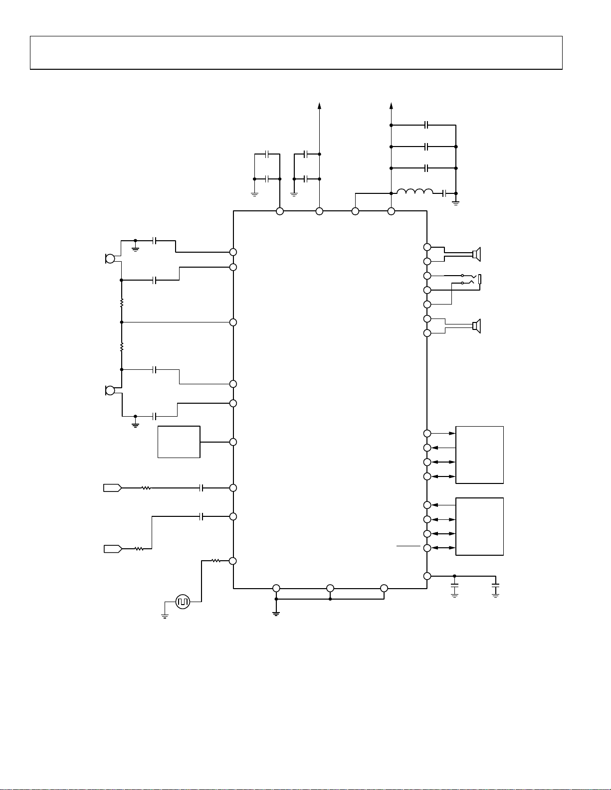
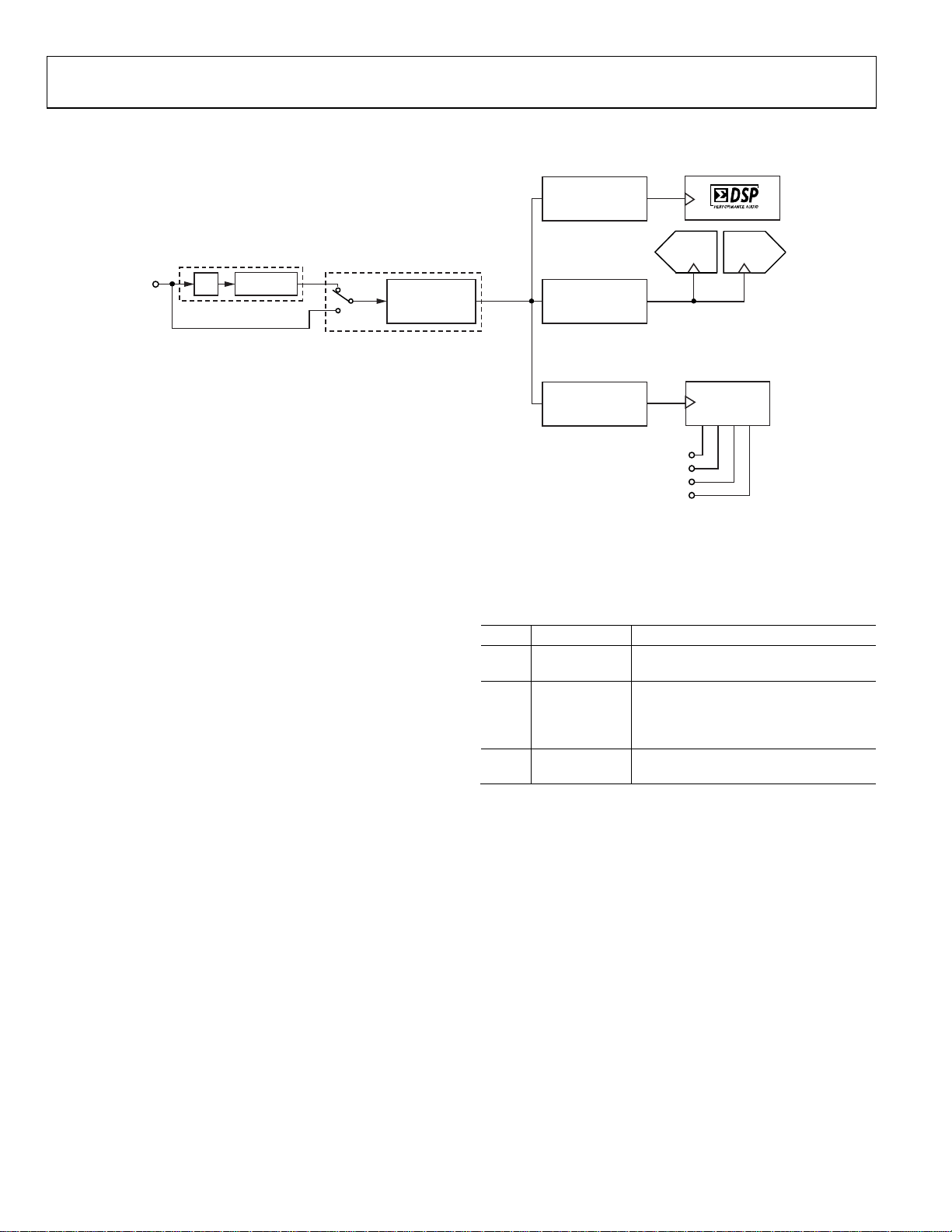
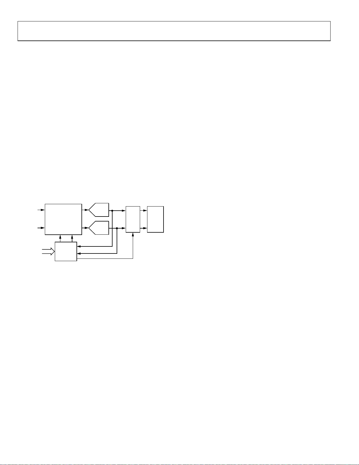
FUNCTIONAL BLOCK DIAGRAM
ADAU1461
GENERAL DESCRIPTION
The ADAU1461 is a low power, stereo audio codec with
integrated digital audio processing that supports stereo 48 kHz
record and playback at 35 mW from a 3.3 V analog supply. The
stereo audio ADCs and DACs support sample rates from 8 kHz
to 96 kHz as well as a digital volume control.
The SigmaDSP® core features 28-bit processing (56-bit double
precision). The processor allows system designers to compensate
for the real-world limitations of microphones, speakers, amplifiers,
and listening environments, resulting in a dramatic improvement
in the perceived audio quality through equalization, multiband
compression, limiting, and third-party branded algorithms.
The SigmaStudio™ graphical development tool is used to program
the ADAU1461. This software includes audio processing blocks
such as filters, dynamics processors, mixers, and low level DSP
functions for fast development of custom signal flows.
The record path includes an integrated microphone bias circuit
and six inputs. The inputs can be mixed and muxed before the
ADC, or they can be configured to bypass the ADC. The
ADAU1461 includes a stereo digital microphone input.
The ADAU1461 includes five high power output drivers (two
differential and three single-ended), supporting stereo headphones, an earpiece, or other output transducer. AC-coupled
or capless configurations are supported. Individual fine level
controls are supported on all analog outputs. The output mixer
stage allows for flexible routing of audio.
CM
IOVDD
DGND
ACKDET/MI CIN
LAUX
LINP
LINN
RINP
RINN
RAUX
MICBI AS
INPUT
MIXERS
ALC
MICRO PHONE
BIAS
DVDDOUT
HP JACK
DETECTION
ADC
ADC DAC
PLL
INPUT/OUTPUT PORTS
MCLK
ADC
DIGI TAL
FILTERS
SERIAL DATA
GPIO1
BCLK/
GPIO2
DC_SDATA/
REGULATOR
DAC
DIGITAL
FILTERS
GPIO3
LRCLK/
AGND
AVDD
AVDD
AGND
ADAU1461
LOUTP
SDA/
COUT
LOUTN
LHP
MONOOUT
RHP
ROUTP
ROUTN
8914-001
DAC
OUTPUT
MIXERS
2
I
C/SPI
CONTROL PORT
SCL/
ADDR1/
ADDR0/
CLATCH
GPIO0
DAC_SDATA/
CDATA
CCLK
Figure 1.
Rev. 0
Information furnished by Analog Devices is believed to be accurate and reliable. However, no
responsibility is assumed by Analog Devices for its use, nor for any infringements of patents or other
rights of third parties that may result from its use. Specifications subject to change without notice. No
license is granted by implication or otherwise under any patent or patent rights of Analog Devices.
Trademarks and registered trademarks are the property of their respective owners.
One Technology Way, P.O. Box 9106, Norwood, MA 02062-9106, U.S.A.
Tel: 781.329.4700 www.analog.com
Fax: 781.461.3113 ©2010 Analog Devices, Inc. All rights reserved.

ADAU1461
TABLE OF CONTENTS
Features .............................................................................................. 1
Applications ....................................................................................... 1
General Description ......................................................................... 1
Functional Block Diagram .............................................................. 1
Revision History ............................................................................... 2
Specifications ..................................................................................... 3
Analog Performance Specifications, TA = 25°C ....................... 3
Analog Performance Specifications, −40°C < TA < +105°C ... 5
Power Supply Specifications........................................................ 7
Digital Filters ................................................................................. 8
Digital Input/Output Specifications........................................... 8
Digital Timing Specifications ..................................................... 9
Digital Timing Diagrams........................................................... 10
Absolute Maximum Ratings .......................................................... 12
Thermal Resistance .................................................................... 12
ESD Caution ................................................................................ 12
Pin Configuration and Function Descriptions ........................... 13
Typical Performance Characteristics ........................................... 15
System Block Diagrams ................................................................. 18
Theory of Operation ...................................................................... 21
Startup, Initialization, and Power ................................................. 22
Power-Up Sequence ................................................................... 22
Power Reduction Modes ............................................................ 22
Digital Power Supply .................................................................. 22
Input/Output Power Supply ...................................................... 22
Clock Generation and Management ........................................ 22
Clocking and Sampling Rates ....................................................... 24
Core Clock ................................................................................... 24
Sampling Rates ............................................................................ 25
PLL ............................................................................................... 25
Record Signal Path .......................................................................... 27
Input Signal Paths ....................................................................... 27
Analog-to-Digital Converters ................................................... 29
Automatic Level Control (ALC) ................................................... 30
ALC Parameters .......................................................................... 30
Noise Gate Function .................................................................. 31
REVISION HISTORY
6/10—Revision 0: Initial Version
Playback Signal Path ...................................................................... 33
Output Signal Paths ................................................................... 33
Headphone Output .................................................................... 34
Pop-and-Click Suppression ...................................................... 35
Line Outputs ............................................................................... 35
Control Ports ................................................................................... 36
Burst Mode Writing and Reading ............................................ 36
I2C Port ........................................................................................ 36
SPI Port ........................................................................................ 39
Serial Data Input/Output Ports .................................................... 40
Applications Information .............................................................. 42
Power Supply Bypass Capacitors .............................................. 42
GSM Noise Filter ........................................................................ 42
Grounding ................................................................................... 42
Exposed Pad PCB Design ......................................................... 42
DSP Core ......................................................................................... 43
Signal Processing ........................................................................ 43
Architecture ................................................................................ 43
Program Counter ....................................................................... 43
Features ........................................................................................ 43
Startup .......................................................................................... 43
Numeric Formats ....................................................................... 44
Programming .............................................................................. 44
Program RAM, Parameter RAM, and Data RAM ..................... 45
Program RAM ............................................................................ 45
Parameter RAM .......................................................................... 45
Data RAM ................................................................................... 45
Read/Write Data Formats ......................................................... 45
Software Safeload ....................................................................... 46
Software Slew .............................................................................. 47
General-Purpose Input/Output .................................................... 48
GPIO Pins Set from the Control Port ...................................... 48
Control Registers ............................................................................ 49
Control Register Details ............................................................ 50
Outline Dimensions ....................................................................... 88
Ordering Guide .......................................................................... 88
Automotive Products ................................................................. 88
Rev. 0 | Page 2 of 88

ADAU1461
SPECIFICATIONS
Supply voltage (AVDD) = 3.3 V, TA = 25°C, master clock = 12.288 MHz (48 kHz fS, 256 × fS mode), input sample rate = 48 kHz, measurement
bandwidth = 20 Hz to 20 kHz, word width = 24 bits, C
(digital output) = 20 pF, I
LOAD
unless otherwise noted. Performance of all channels is identical, exclusive of the interchannel gain mismatch and interchannel phase
deviation specifications.
ANALOG PERFORMANCE SPECIFICATIONS, TA = 25°C
IOVDD = 3.3 V ± 10%.
Table 1.
Parameter Test Conditions/Comments Min Typ Max Unit
ANALOG-TO-DIGITAL CONVERTERS
ADC Resolution All ADCs 24 Bits
Digital Attenuation Step 0.375 dB
Digital Attenuation Range 95 dB
INPUT RESISTANCE
Single-Ended Line Input −12 dB gain 80.4 kΩ
0 dB gain 21 kΩ
6 dB gain 10.5 kΩ
PGA Inverting Inputs −12 dB gain 84.5 kΩ
0 dB gain 53 kΩ
35.25 dB gain 1.7 kΩ
PGA Noninverting Inputs All gains 105 kΩ
SINGLE-ENDED LINE INPUT
Full-Scale Input Voltage (0 dB) 1.0 (2.83) V rms (V p-p)
Dynamic Range 20 Hz to 20 kHz, −60 dB input
With A-Weighted Filter (RMS) 83.5 99 dB
No Filter (RMS) 83 96 dB
Total Harmonic Distortion + Noise −1 dBFS −90 −71 dB
Signal-to-Noise Ratio
With A-Weighted Filter (RMS) 99 dB
No Filter (RMS) 96 dB
Input Mixer Gain per Step −12 dB to +6 dB range 2.89 3 3.07 dB
Mute Attenuation
Interchannel Gain Mismatch −0.3 +0.032 +0.3 dB
Offset Error −5 0 +5 mV
Gain Error −17 −12 −8 %
Interchannel Isolation 68 dB
Power Supply Rejection Ratio CM capacitor = 20 F, 100 mV p-p @ 1 kHz 67 dB
PSEUDO-DIFFERENTIAL PGA INPUT
Full-Scale Input Voltage (0 dB) 1.0 (2.83) V rms (V p-p)
Dynamic Range 20 Hz to 20 kHz, −60 dB input
With A-Weighted Filter (RMS) 94 98 dB
No Filter (RMS) 91 95 dB
Total Harmonic Distortion + Noise −1 dBFS −89 −83 dB
Signal-to-Noise Ratio
With A-Weighted Filter (RMS) 98 dB
No Filter (RMS) 95 dB
PGA Boost Gain Error
ADC performance excludes mixers
and PGA
LINPG[2:0], LINNG[2:0] = 000,
RINPG[2:0], RINNG[2:0] = 000,
MX1AUXG[2:0], MX2AUXG[2:0] = 000
20 dB gain setting (RDBOOST[1:0],
LDBOOST[1:0] = 10)
(digital output) = 2 mA, VIH = 2 V, VIL = 0.8 V,
LOAD
−85.5 −77 dB
−8 +0.4 +8 dB
Rev. 0 | Page 3 of 88

ADAU1461
Parameter Test Conditions/Comments Min Typ Max Unit
Mute Attenuation PGA muted
LDMUTE, RDMUTE = 0 −76 −73 dB
RDBOOST[1:0], LDBOOST[1:0] = 00 −87 −82 dB
Interchannel Gain Mismatch −0.6 −0.073 +0.6 dB
Offset Error −6 0 +6 mV
Gain Error −24 −14 −3 %
Interchannel Isolation 83 dB
Common-Mode Rejection Ratio 100 mV rms, 1 kHz −58 dB
100 mV rms, 20 kHz −52 −48 −44 dB
FULL DIFFERENTIAL PGA INPUT Differential PGA inputs
Full-Scale Input Voltage (0 dB) 1.0 (2.83) V rms (V p-p)
Dynamic Range 20 Hz to 20 kHz, −60 dB input
With A-Weighted Filter (RMS) 94 98 dB
No Filter (RMS) 91 95 dB
Total Harmonic Distortion + Noise −1 dBFS −78 −74 dB
Signal-to-Noise Ratio
With A-Weighted Filter (RMS) 98 dB
No Filter (RMS) 95 dB
PGA Boost Gain Error
Mute Attenuation PGA muted
LDMUTE, RDMUTE = 0 −76 −73 dB
RDBOOST[1:0], LDBOOST[1:0] = 00 −87 −82 dB
Interchannel Gain Mismatch −0.3 −0.0005 +0.3 dB
Offset Error −6 0 +6 mV
Gain Error −17 −14 −9 %
Interchannel Isolation 83 dB
Common-Mode Rejection Ratio 100 mV rms, 1 kHz −58 dB
100 mV rms, 20 kHz −52 −48 −44 dB
MICROPHONE BIAS MBIEN = 1
Bias Voltage
0.65 × AVDD MBI = 1, MPERF = 0 2.00 2.145 2.19 V
MBI = 1, MPERF = 1 2.04 2.13 2.21 V
0.90 × AVDD MBI = 0, MPERF = 0 2.89 2.97 3.04 V
MBI = 0, MPERF = 1 2.89 2.99 3.11 V
Bias Current Source MBI = 0, MPERF = 1 3 mA
Noise in the Signal Bandwidth 1 kHz to 20 kHz
MBI = 0, MPERF = 0 42 nV/√Hz
MBI = 0, MPERF = 1 85 nV/√Hz
MBI = 1, MPERF = 0 25 nV/√Hz
MBI = 1, MPERF = 1 13 22 36 nV/√Hz
DIGITAL-TO-ANALOG CONVERTERS
DAC Resolution All DACs 24 Bits
Digital Attenuation Step 0.375 dB
Digital Attenuation Range 95 dB
DAC TO LINE OUTPUT
Full-Scale Output Voltage (0 dB) 0.92 (2.60) V rms (V p-p)
Dynamic Range
With A-Weighted Filter (RMS) 95 101 dB
No Filter (RMS) 93.5 98 dB
20 dB gain setting (RDBOOST[1:0],
LDBOOST[1:0] = 10)
DAC performance excludes mixers and
headphone amplifier
20 Hz to 20 kHz, −60 dBFS input, line
output mode
−8 −0.15 +8 dB
Rev. 0 | Page 4 of 88
ADAU1461
Parameter Test Conditions/Comments Min Typ Max Unit
Total Harmonic Distortion + Noise 0 dBFS, 10 kΩ load
Line Output Mode −92 −77 dB
Headphone Output Mode −89 −79 dB
Signal-to-Noise Ratio Line output mode
With A-Weighted Filter (RMS) 101 dB
No Filter (RMS) 98 dB
Mute Attenuation
Mixer 3 and Mixer 4 Muted
Mixer 5, Mixer 6, and Mixer 7 Muted
All Volume Controls Muted LOUTM, ROUTM = 0 −82 −74 dB
MONOM, LHPM, RHPM = 0 −74 −69 dB
Interchannel Gain Mismatch −0.3 −0.005 +0.3 dB
Offset Error −22 0 +22 mV
Gain Error −10 +3 +10 %
Interchannel Isolation 1 kHz, 0 dBFS input signal 100 dB
Power Supply Rejection Ratio CM capacitor = 20 F, 100 mV p-p @ 1 kHz 70 dB
DAC TO HEADPHONE/EARPIECE
OUTPUT
Full-Scale Output Voltage (0 dB) Scales linearly with AVDD 0.92 (2.60) V rms (V p-p)
Total Harmonic Distortion + Noise −4 dBFS, 16 Ω load, PO = 21.1 mW −82 dB
−4 dBFS, 32 Ω load, PO = 10.6 mW −82 dB
Capless Headphone Mode −2 dBFS, 16 Ω load −78 −71 dB
−2 dBFS, 32 Ω load −75 −65 dB
Headphone Output Mode 0 dBFS, 10 kΩ load −86 −77 dB
Interchannel Isolation 1 kHz, 0 dBFS input signal, 32 Ω load
Referred to GND 73 dB
Power Supply Rejection Ratio CM capacitor = 20 F, 100 mV p-p @ 1 kHz 67 dB
REFERENCE
Common-Mode Reference Output CM pin 1.62 1.65 1.67 V
MX3RM, MX3LM, MX4RM, MX4LM = 0,
MX3AUXG[3:0], MX4AUXG[3:0] = 0000,
MX3G1[3:0], MX3G2[3:0] = 0000,
MX4G1[3:0], MX4G2[3:0] = 0000
MX5G3[1:0], MX5G4[1:0], MX6G3[1:0],
MX6G4[1:0], MX7[1:0] = 00
LOUTx, ROUTx, LHP, RHP in headphone
output mode; P
channel
Referred to CM (capless headphone
mode)
= output power per
O
−85 −78 dB
−89 −80 dB
50 dB
ANALOG PERFORMANCE SPECIFICATIONS, −40°C < TA < +105°C
IOVDD = 3.3 V ± 10%.
Table 2.
Parameter Test Conditions/Comments Min Typ Max Unit
SINGLE-ENDED LINE INPUT
Dynamic Range 20 Hz to 20 kHz, −60 dB input
With A-Weighted Filter (RMS) 74 dB
No Filter (RMS) 71 dB
Total Harmonic Distortion + Noise −1 dBFS −67 dB
Input Mixer Gain per Step −12 dB to +6 dB range 2.88 3.09 dB
Mute Attenuation
Interchannel Gain Mismatch −0.5 +0.5 dB
Offset Error −5 +5 mV
Gain Error −22 −6 %
LINPG[2:0], LINNG[2:0] = 000,
RINPG[2:0], RINNG[2:0] = 000,
MX1AUXG[2:0], MX2AUXG[2:0] = 000
Rev. 0 | Page 5 of 88
−77 dB

ADAU1461
Parameter Test Conditions/Comments Min Typ Max Unit
PSEUDO-DIFFERENTIAL PGA INPUT
Dynamic Range 20 Hz to 20 kHz, −60 dB input
With A-Weighted Filter (RMS) 94 dB
No Filter (RMS) 91 dB
Total Harmonic Distortion + Noise −1 dBFS −75 dB
PGA Boost Gain Error
Mute Attenuation PGA muted
LDMUTE, RDMUTE = 0 −73 dB
RDBOOST[1:0], LDBOOST[1:0] = 00 −82 dB
Interchannel Gain Mismatch −0.6 +0.6 dB
Offset Error −6 +6 mV
Gain Error −24 −3 %
Common-Mode Rejection Ratio 100 mV rms, 1 kHz −64 −38 dB
100 mV rms, 20 kHz −53 −43 dB
FULL DIFFERENTIAL PGA INPUT Differential PGA inputs
Dynamic Range 20 Hz to 20 kHz, −60 dB input
With A-Weighted Filter (RMS) 89 dB
No Filter (RMS) 86 dB
Total Harmonic Distortion + Noise −1 dBFS −70 dB
PGA Boost Gain Error
Mute Attenuation PGA muted
LDMUTE, RDMUTE = 0 −73 dB
RDBOOST[1:0], LDBOOST[1:0] = 00 −82 dB
Interchannel Gain Mismatch −0.4 +0.4 dB
Offset Error −6 +6 mV
Gain Error −21 −7 %
Common-Mode Rejection Ratio 100 mV rms, 1 kHz −64 −38 dB
100 mV rms, 20 kHz −53 −43 dB
MICROPHONE BIAS MBIEN = 1
Bias Voltage
0.65 × AVDD MBI = 1, MPERF = 0 1.85 2.45 V
MBI = 1, MPERF = 1 1.87 2.45 V
0.90 × AVDD MBI = 0, MPERF = 0 2.65 3.40 V
MBI = 0, MPERF = 1 2.65 3.40 V
Noise in the Signal Bandwidth 1 kHz to 20 kHz 11 36 nV/√Hz
DAC TO LINE OUTPUT
Dynamic Range
With A-Weighted Filter (RMS) 85 dB
No Filter (RMS) 78 dB
Total Harmonic Distortion + Noise 0 dBFS, 10 kΩ load
Line Output Mode −76 dB
Headphone Output Mode −78 dB
Mute Attenuation
Mixer 3 and Mixer 4 Muted
Mixer 5, Mixer 6, and Mixer 7 Muted
All Volume Controls Muted LOUTM, ROUTM = 0 −74 dB
MONOM, LHPM, RHPM = 0 −69 dB
20 dB gain setting (RDBOOST[1:0],
LDBOOST[1:0] = 10)
20 dB gain setting (RDBOOST[1:0],
LDBOOST[1:0] = 10)
20 Hz to 20 kHz, −60 dB input, line
output mode
MX3RM, MX3LM, MX4RM, MX4LM = 0,
MX3AUXG[3:0], MX4AUXG[3:0] = 0000,
MX3G1[3:0], MX3G2[3:0] = 0000,
MX4G1[3:0], MX4G2[3:0] = 0000
MX5G3[1:0], MX5G4[1:0], MX6G3[1:0],
MX6G4[1:0], MX7[1:0] = 00
−11 −7 dB
−11 −7 dB
−77 dB
−77 dB
Rev. 0 | Page 6 of 88
ADAU1461
Parameter Test Conditions/Comments Min Typ Max Unit
Interchannel Gain Mismatch −0.3 +0.3 dB
Offset Error −22 +22 mV
Gain Error −10 +10 %
DAC TO HEADPHONE/EARPIECE
OUTPUT
LOUTx, ROUTx, LHP, RHP in headphone
output mode; P
= output power per
O
channel
Total Harmonic Distortion + Noise
Capless Headphone Mode −2 dBFS, 16 Ω load −61 dB
−2 dBFS, 32 Ω load −63 dB
Headphone Output Mode 0 dBFS, 10 kΩ load −76 dB
REFERENCE
Common-Mode Reference Output CM pin 1.47 1.83 V
POWER SUPPLY SPECIFICATIONS
Master clock = 12.288 MHz, input sample rate = 48 kHz, input tone = 1 kHz, ADC input @ −1 dBFS, DAC input @ 0 dBFS,
−40°C < T
Table 3.
Parameter Test Conditions/Comments Min Typ Max Unit
SUPPLIES
Voltage DVDDOUT 1.56 V
AVDD 2.97 3.3 3.65 V
IOVDD 2.97 3.3 3.65 V
Digital I/O Current (IOVDD) 20 pF capacitive load on all digital pins
f
f
Analog Current (AVDD)
< +105°C, IOVDD = 3.3 V ± 10%. For total power consumption, add the IOVDD current listed in Tabl e 3.
A
Slave Mode fS = 48 kHz 0.48 mA
= 96 kHz 0.9 mA
S
f
= 8 kHz 0.13 mA
S
Master Mode fS = 48 kHz 1.51 mA
= 96 kHz 3 mA
S
f
= 8 kHz 0.27 mA
S
Record Stereo Differential to ADC
PLL bypass 5.24 mA
Integer PLL 6.57 mA
DAC Stereo Playback to Line Output 10 kΩ load
PLL bypass 5.55 mA
Integer PLL 6.90 mA
DAC Stereo Playback to Headphone 32 Ω load
PLL bypass 30.9 mA
Integer PLL 32.25 mA
DAC Stereo Playback to Capless Headphone 32 Ω load
PLL bypass 56.75 mA
Integer PLL 58 mA
Rev. 0 | Page 7 of 88
ADAU1461
DIGITAL FILTERS
Table 4.
Parameter Mode Factor Min Typ Max Unit
ADC DECIMATION FILTER All modes, typ @ 48 kHz
Pass Band 0.4375 fS 21 kHz
Pass-Band Ripple ±0.015 dB
Transition Band 0.5 fS 24 kHz
Stop Band 0.5625 fS 27 kHz
Stop-Band Attenuation 67 dB
Group Delay 22.9844/fS 479 µs
DAC INTERPOLATION FILTER
Pass Band 48 kHz mode, typ @ 48 kHz 0.4535 fS 22 kHz
96 kHz mode, typ @ 96 kHz 0.3646 fS 35 kHz
Pass-Band Ripple 48 kHz mode, typ @ 48 kHz ±0.01 dB
96 kHz mode, typ @ 96 kHz ±0.05 dB
Transition Band 48 kHz mode, typ @ 48 kHz 0.5 fS 24 kHz
96 kHz mode, typ @ 96 kHz 0.5 fS 48 kHz
Stop Band 48 kHz mode, typ @ 48 kHz 0.5465 fS 26 kHz
96 kHz mode, typ @ 96 kHz 0.6354 fS 61 kHz
Stop-Band Attenuation 48 kHz mode, typ @ 48 kHz 69 dB
96 kHz mode, typ @ 96 kHz 68 dB
Group Delay 48 kHz mode, typ @ 48 kHz 25/fS 521 µs
96 kHz mode, typ @ 96 kHz 11/fS 115 µs
DIGITAL INPUT/OUTPUT SPECIFICATIONS
−40°C < TA < +105°C, IOVDD = 3.3 V ± 10%.
Table 5.
Parameter Test Conditions/Comments Min Typ Max Unit
INPUT SPECIFICATIONS
Input Voltage High (VIH) 0.7 × IOVDD V
Input Voltage Low (VIL) 0.3 × IOVDD V
Input Leakage
Pull-Ups/Pull-Downs Disabled IIH @ VIH = 3.3 V −0.17 +0.17 µA
I
I
Pull-Ups Enabled IIH @ VIH = 3.3 V −0.7 +0.7 µA
I
Pull-Downs Enabled IIH @ VIH = 3.3 V 2.7 8.3 µA
I
Input Capacitance 5 pF
OUTPUT SPECIFICATIONS
Output Voltage High (VOH) IOH = 2 mA @ 3.3 V 0.8 × IOVDD V
Output Voltage Low (VOL) IOL = 2 mA @ 3.3 V 0.1 × IOVDD V
@ VIL = 0 V −0.17 +0.17 µA
IL
@ VIL = 0 V (MCLK pin) −13.5 −0.5 µA
IL
@ VIL = 0 V −13.5 −0.5 µA
IL
@ VIL = 0 V −0.18 +0.18 µA
IL
Rev. 0 | Page 8 of 88
ADAU1461
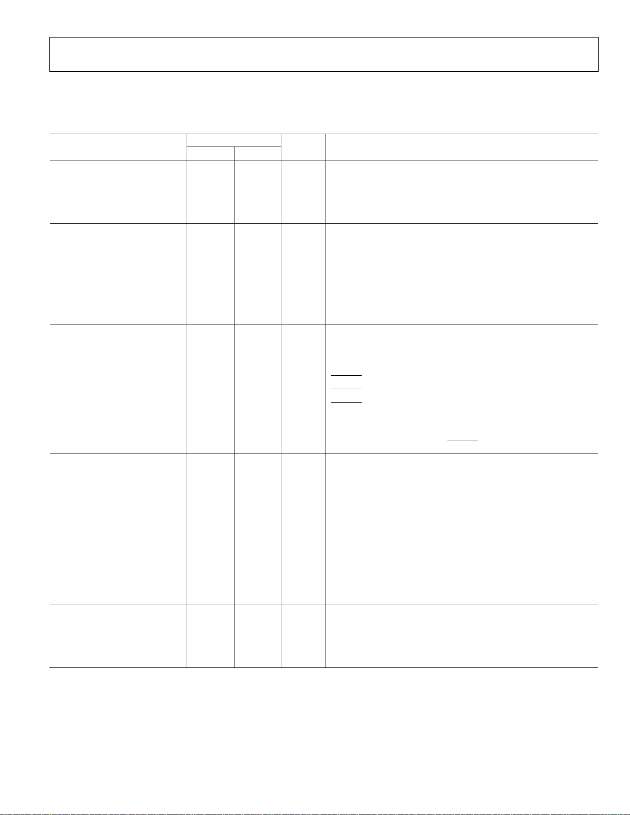
DIGITAL TIMING SPECIFICATIONS
−40°C < TA < +105°C, IOVDD = 3.3 V ± 10%.
Table 6. Digital Timing
Limit
Parameter
t
MIN
MAX
MASTER CLOCK
tMP 74 488 ns MCLK period, 256 × fS mode.
tMP 37 244 ns MCLK period, 512 × fS mode.
tMP 24.7 162.7 ns MCLK period, 768 × fS mode.
tMP 18.5 122 ns MCLK period, 1024 × fS mode.
SERIAL PORT
t
5 ns BCLK pulse width low.
BIL
t
5 ns BCLK pulse width high.
BIH
t
5 ns LRCLK setup. Time to BCLK rising.
LIS
t
5 ns LRCLK hold. Time from BCLK rising.
LIH
t
5 ns DAC_SDATA setup. Time to BCLK rising.
SIS
t
5 ns DAC_SDATA hold. Time from BCLK rising.
SIH
t
50 ns ADC_SDATA delay. Time from BCLK falling in master mode.
SODM
SPI PORT
f
10 MHz CCLK frequency.
CCLK
t
10 ns CCLK pulse width low.
CCPL
t
10 ns CCLK pulse width high.
CCPH
t
5 ns
CLS
t
10 ns
CLH
t
10 ns
CLPH
t
5 ns CDATA setup. Time to CCLK rising.
CDS
t
5 ns CDATA hold. Time from CCLK rising.
CDH
t
50 ns
COD
I2C PORT
f
400 kHz SCL frequency.
SCL
t
0.6 µs SCL high.
SCLH
t
1.3 µs SCL low.
SCLL
t
0.6 µs Setup time; relevant for repeated start condition.
SCS
t
0.6 µs Hold time. After this period, the first clock is generated.
SCH
tDS 100 ns Data setup time.
t
300 ns SCL rise time.
SCR
t
300 ns SCL fall time.
SCF
t
300 ns SDA rise time.
SDR
t
300 ns SDA fall time.
SDF
t
0.6 µs Bus-free time. Time between stop and start.
BFT
DIGITAL MICROPHONE R
t
10 ns Digital microphone clock fall time.
DCF
t
10 ns Digital microphone clock rise time.
DCR
t
22 30 ns Digital microphone delay time for valid data.
DDV
t
0 12 ns Digital microphone delay time for data three-stated.
DDH
Unit Description t
CLATCH
CLATCH
CLATCH
COUT three-stated. Time from CLATCH
setup. Time to CCLK rising.
hold. Time from CCLK rising.
pulse width high.
= 1 MΩ, C
LOAD
LOAD
= 14 pF.
rising.
Rev. 0 | Page 9 of 88
ADAU1461
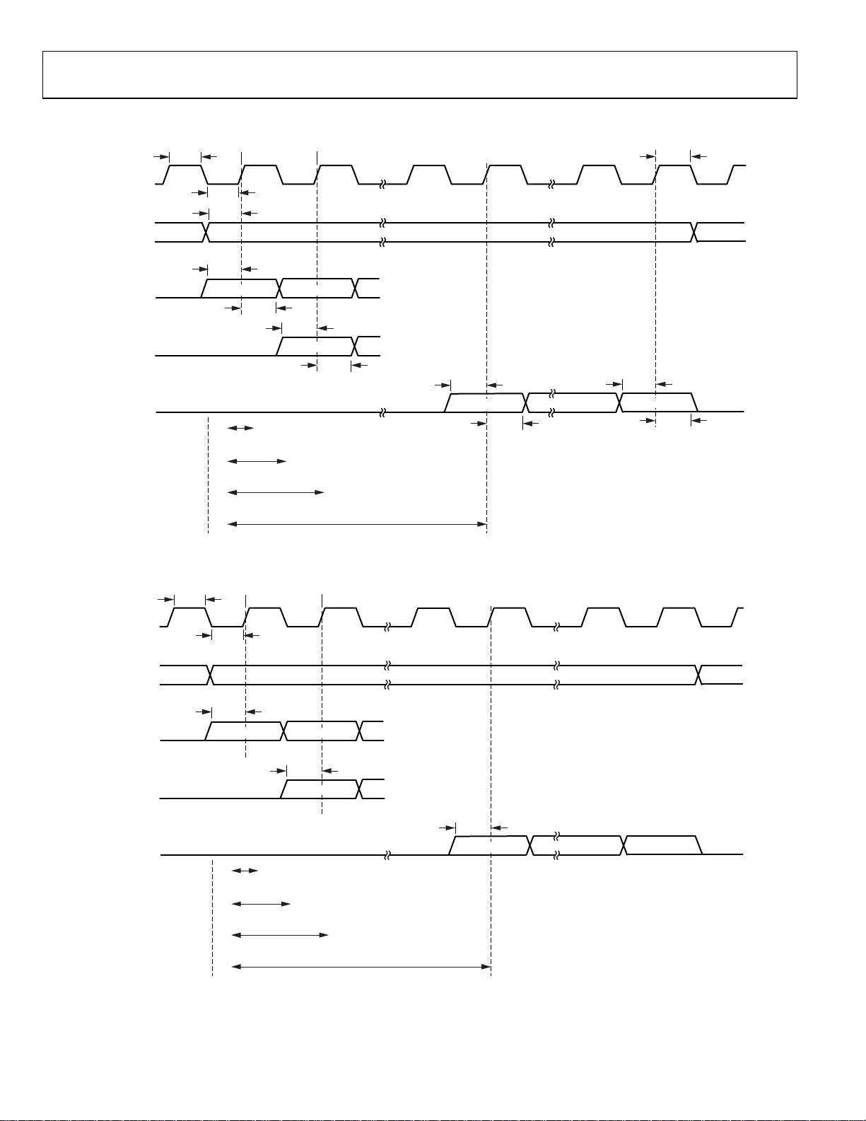
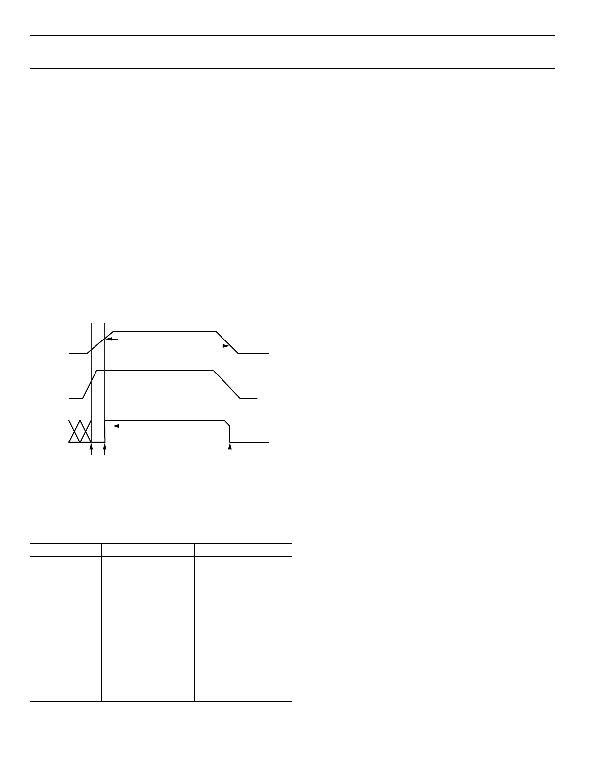
DIGITAL TIMING DIAGRAMS
t
LIH
t
SIS
LSB
t
SIH
08914-002
RIGHT-JUSTIFIED
BCLK
LRCLK
DAC_SDATA
LEFT-JUSTIFIED
MODE
DAC_SDATA
2
I
S MODE
DAC_SDATA
MODE
BCLK
t
BIH
t
BIL
t
LIS
t
SIS
MSB
t
SIH
8-BIT CLOCKS
(24-BIT DATA)
12-BIT CLOCKS
(20-BIT DATA)
14-BIT CLOCKS
(18-BIT DATA)
16-BIT CLOCKS
(16-BIT DATA)
t
SIS
MSB – 1
MSB
t
SIH
t
SIS
MSB
t
SIH
Figure 2. Serial Input Port Timing
t
BIH
t
BIL
LRCLK
ADC_SDATA
LEFT-JUSTIFIED
MODE
ADC_SDATA
2
I
S MODE
ADC_SDATA
RIGHT -JUSTI FIED
MODE
t
SODM
MSB
8-BIT CLOCKS
(24-BIT DATA)
12-BIT CLO CKS
(20-BIT DATA)
14-BIT CLO CKS
(18-BIT DATA)
16-BIT CLO CKS
(16-BIT DATA)
t
SODM
MSB – 1
MSB
Figure 3. Serial Output Port Timing
Rev. 0 | Page 10 of 88
t
SODM
MSB
LSB
08914-003
ADAU1461
t
CLS
t
CCPL
CLATCH
CCLK
CDATA
COUT
t
CDS
t
CCPH
t
CDH
Figure 4. SPI Port Timing
t
t
SCLH
DS
t
SCH
SDA
t
SCH
t
SCR
t
CLH
t
COD
t
CLPH
08914-004
SCL
t
SCLL
t
SCF
Figure 5. I
t
2
C Port Timing
SCS
t
BFT
08914-005
t
CLK
DATA1/
DATA1 DATA1 DATA2DATA2
DATA2
DCF
t
DDH
t
DDH
t
DDV
t
DCR
t
DDV
08914-006
Figure 6. Digital Microphone Timing
Rev. 0 | Page 11 of 88
ADAU1461
ABSOLUTE MAXIMUM RATINGS
Table 7.
Parameter Rating
Power Supply (AVDD) −0.3 V to +3.65 V
Input Current (Except Supply Pins) ±20 mA
Analog Input Voltage (Signal Pins) −0.3 V to AVDD + 0.3 V
Digital Input Voltage (Signal Pins) −0.3 V to IOVDD + 0.3 V
Operating Temperature Range −40°C to +105°C
Storage Temperature Range −65°C to +150°C
Stresses above those listed under Absolute Maximum Ratings
may cause permanent damage to the device. This is a stress
rating only; functional operation of the device at these or any
other conditions above those indicated in the operational
section of this specification is not implied. Exposure to absolute
maximum rating conditions for extended periods may affect
device reliability.
THERMAL RESISTANCE
θJA represents thermal resistance, junction-to-ambient; θJC represents thermal resistance, junction-to-case. All characteristics are
for a 4-layer board.
Table 8. Thermal Resistance
Package Type θJA θ
32-Lead LFCSP 50.1 17 °C/W
Unit
JC
ESD CAUTION
Rev. 0 | Page 12 of 88
ADAU1461
PIN CONFIGURATION AND FUNCTION DESCRIPTIONS
SCL/CCLK
SDA/COUT
ADDR1/CDATA
LRCLK/GPI O3
BCLK/GPIO 2
DAC_SDATA/GPI O0
ADC_SDATA/GPI O1
DGND
28
27
26
25
29
31
30
32
14
15
RAUX
ROUTP
24 DVDDOUT
23 AVDD
22 AGND
21 MONOOUT
20 LHP
19 RHP
18 LOUTP
17 LOUTN
16
ROUTN
08914-007
1IOVDD
PIN 1
2MCLK
INDICATOR
3ADDR0/CLATCH
4JACKDET/MICI N
ADAU1461
5MICBIAS
TOP VIEW
6LAUX
(Not to Scale)
7CM
8AVDD
9
11
12
13
10
LINP
LINN
RINP
RINN
AGND
NOTES
1. THE EXPOSED PAD IS CONNECTED INT ERNALLY TO THE
ADAU1461 GROUNDS. FOR INCREASED REL IABILITY OF T HE
SOLDER JOINTS AND MAXIMUM THERMAL CAPABILITY, IT IS
RECOMMENDED THAT THE PAD BE SOL DERED TO THE
GROUND PLANE.
Figure 7. Pin Configuration
Table 9. Pin Function Descriptions
Pin No. Mnemonic Type
1 IOVDD PWR
1
Description
Supply for Digital Input and Output Pins. The digital output pins are supplied from IOVDD,
which also sets the highest input voltage that should be seen on the digital input pins.
IOVDD should be set to 3.3 V. The current draw of this pin is variable because it is dependent
on the loads of the digital outputs. IOVDD should be decoupled to DGND with a 100 nF
capacitor and a 10 F capacitor.
2 MCLK D_IN External Master Clock Input.
3
ADDR0/CLATCH
D_IN I2C Address Bit 0 (ADDR0).
SPI Latch Signal (CLATCH
). Must go low at the beginning of an SPI transaction and high at the
end of a transaction. Each SPI transaction can take a different number of CCLKs to complete,
depending on the address and read/write bit that are sent at the beginning of the SPI
transaction.
4 JACKDET/MICIN D_IN Detect Insertion/Removal of Headphone Plug (JACKDET).
Digital Microphone Stereo Input (MICIN).
5 MICBIAS A_OUT Bias Voltage for Electret Microphone.
6 LAUX A_IN Left Channel Single-Ended Auxiliary Input. Biased at AVDD/2.
7 CM A_OUT
AVDD/2 V Common-Mode Reference. A 10 F to 47 F standard decoupling capacitor should
be connected between this pin and AGND to reduce crosstalk between the ADCs and DACs.
This pin can be used to bias external analog circuits, as long as they are not drawing current
from CM (for example, the noninverting input of an op amp).
8 AVDD PWR
3.3 V Analog Supply for DAC and Microphone Bias. This pin should be decoupled locally to
AGND with a 100 nF capacitor.
9 AGND PWR
Analog Ground. The AGND and DGND pins can be tied together on a common ground plane.
AGND should be decoupled locally to AVDD with a 100 nF capacitor.
10 LINP A_IN Left Channel Noninverting Input or Single-Ended Input 0. Biased at AVDD/2.
11 LINN A_IN Left Channel Inverting Input or Single-Ended Input 1. Biased at AVDD/2.
12 RINP A_IN Right Channel Noninverting Input or Single-Ended Input 2. Biased at AVDD/2.
13 RINN A_IN Right Channel Inverting Input or Single-Ended Input 3. Biased at AVDD/2.
14 RAUX A_IN Right Channel Single-Ended Auxiliary Input. Biased at AVDD/2.
15 ROUTP A_OUT Right Line Output, Positive. Biased at AVDD/2.
16 ROUTN A_OUT Right Line Output, Negative. Biased at AVDD/2.
17 LOUTN A_OUT Left Line Output, Negative. Biased at AVDD/2.
18 LOUTP A_OUT Left Line Output, Positive. Biased at AVDD/2.
Rev. 0 | Page 13 of 88

ADAU1461
Pin No. Mnemonic Type
1
Description
19 RHP A_OUT Right Headphone Output. Biased at AVDD/2.
20 LHP A_OUT Left Headphone Output. Biased at AVDD/2.
21 MONOOUT A_OUT
Mono Output or Virtual Ground for Capless Headphone. Biased at AVDD/2 when set as mono
output.
22 AGND PWR
Analog Ground. The AGND and DGND pins can be tied together on a common ground plane.
AGND should be decoupled locally to AVDD with a 100 nF capacitor.
23 AVDD PWR
3.3 V Analog Supply for ADC, Output Driver, and Input to Digital Supply Regulator. This pin
should be decoupled locally to AGND with a 100 nF capacitor.
24 DVDDOUT PWR
Digital Core Supply Decoupling Point. The digital supply is generated from an on-board
regulator and does not require an external supply. DVDDOUT should be decoupled to DGND
with a 100 nF capacitor and a 10 F capacitor.
25 DGND PWR
Digital Ground. The AGND and DGND pins can be tied together on a common ground plane.
DGND should be decoupled to DVDDOUT and to IOVDD with 100 nF capacitors and 10 F
capacitors.
26 ADC_SDATA/GPIO1 D_IO ADC Serial Output Data (ADC_SDATA).
General-Purpose Input/Output 1 (GPIO1).
27 DAC_SDATA/GPIO0 D_IO DAC Serial Input Data (DAC_SDATA).
General-Purpose Input/Output 0 (GPIO0).
28 BCLK/GPIO2 D_IO Serial Data Port Bit Clock (BCLK).
General-Purpose Input/Output 2 (GPIO2).
29 LRCLK/GPIO3 D_IO Serial Data Port Frame Clock (LRCLK).
General-Purpose Input/Output 3 (GPIO3).
30 ADDR1/CDATA D_IN I2C Address Bit 1 (ADDR1).
SPI Data Input (CDATA).
31 SDA/COUT D_IO
2
C Data (SDA). This pin is a bidirectional open-collector input/output. The line connected to
I
this pin should have a 2 kΩ pull-up resistor.
SPI Data Output (COUT). This pin is used for reading back registers and memory locations. It is
three-state when an SPI read is not active.
32 SCL/CCLK D_IN
2
C Clock (SCL). This pin is always an open-collector input when in I2C control mode. The line
I
connected to this pin should have a 2 kΩ pull-up resistor.
SPI Clock (CCLK). This pin can run continuously or be gated off between SPI transactions.
EP Exposed Pad
Exposed Pad. The exposed pad is connected internally to the ADAU1461 grounds. For
increased reliability of the solder joints and maximum thermal capability, it is recommended
that the pad be soldered to the ground plane. See the Exposed Pad PCB Design section for
more information.
1
A_IN = analog input, A_OUT = analog output, D_IN = digital input, D_IO = digital input/output, PWR = power.
Rev. 0 | Page 14 of 88
ADAU1461
–
TYPICAL PERFORMANCE CHARACTERISTICS
28
26
24
22
20
18
16
14
12
10
8
6
STEREO OUTPUT PO WER (mW)
4
2
0
–60 0–10–20–30–40–50
DIGITAL 1kHz INPUT SIGNAL (dBFS)
Figure 8. Headphone Amplifier Power vs. Input Level, 16 Ω Load
08914-055
30
–35
–40
–45
–50
–55
–60
–65
–70
–75
THD + N (dBV)
–80
–85
–90
–95
–100
–105
–60 0–10–20–30–40–50
DIGITAL 1kHz INPUT SIGNAL (dBFS)
Figure 11. Headphone Amplifier THD + N vs. Input Level, 16 Ω Load
08914-056
18
16
14
12
10
8
6
4
STEREO OUTPUT PO WER (mW)
2
0
–60 0–10–20–30–40–50
DIGITAL 1kHz INPUT SIGNAL (dBFS)
Figure 9. Headphone Amplifier Power vs. Input Level, 32 Ω Load
0
10
20
30
40
50
60
MAGNITUDE (d BFS)
70
80
90
100
0 0.1 0.2 0.3 0.4 0.5 0.6 0.7 0.8 0.9 1.0
FREQUENCY (NORMALIZED T O
f
)
S
Figure 10. ADC Decimation Filter, 64× Oversampling, Normalized to fS
0
–10
–20
–30
–40
–50
–60
THD + N (dBV)
–70
–80
–90
–100
–60 0–10–20–30–40–50
08914-057
DIGITAL 1kHz INPUT SI GNAL (dBFS)
08914-058
Figure 12. Headphone Amplifier THD + N vs. Input Level, 32 Ω Load
0.04
0.02
0
–0.02
MAGNITUDE (dBFS)
–0.04
–0.06
0 0.05 0.10 0.20 0.30 0.400.15 0.25 0. 35
08914-008
FREQUENCY (NORMALIZED TO
f
)
S
08914-009
Figure 13. ADC Decimation Filter Pass-Band Ripple, 64× Oversampling,
Normalized to f
S
Rev. 0 | Page 15 of
88
ADAU1461
0
–10
–20
–30
–40
–50
–60
MAGNITUDE (d BFS)
–70
–80
–90
–100
0.10 0.2 0.3 0. 4 0.5 0.6 0.7 0.8 0.9 1.0
FREQUENCY (NORMALIZED TO
f
)
S
Figure 14. ADC Decimation Filter, 128× Oversampling, Normalized to fS
4-010
0891
0.10
0.08
0.06
0.04
0.02
0
–0.02
MAGNITUDE (d BFS)
–0.04
–0.06
–0.08
–0.10
0 0.05 0.10 0.20 0.30 0.400.15 0.25 0.35 0.500.45
FREQUENCY (NORMALIZED TO
f
)
S
Figure 17. ADC Decimation Filter Pass-Band Ripple, 128× Oversampling,
Normalized to f
S
08914-011
0
–10
–20
–30
–40
–50
–60
MAGNITUDE (d BFS)
–70
–80
–90
–100
0
0.1 0. 2 0.3 0.4 0.5 0. 6 0. 7 0.8 0.9 1.0
FREQUENCY (NORMALIZED TO
f
)
S
4-0120891
Figure 15. ADC Decimation Filter, 128× Oversampling, Double-Rate Mode,
Normalized to f
0
10
20
30
40
50
60
MAGNITUDE (dBFS)
70
80
90
100
0 0.1 0.2 0.3 0.4 0.5 0.6 0.7 0.8 0.9 1.0
FREQUENCY (NORMALIZED TO
S
f
)
S
8914-014
Figure 16. DAC Interpolation Filter, 64× Oversampling, Double-Rate Mode,
Normalized to f
S
0.04
0.02
0
0.02
MAGNITUDE (dBFS)
0.04
0.06
0 0.05 0.10 0.20 0.30 0.400.15 0.25 0. 35
FREQUENCY (NO RMALIZED T O
f
)
S
Figure 18. ADC Decimation Filter Pass-Band Ripple, 128× Oversampling,
Double-Rate Mode, Normalized to f
0.20
0.15
0.10
0.05
0
–0.05
MAGNITUDE (dBFS)
–0.10
–0.15
–0.20
0 0.05 0.10 0.20 0.30 0.400. 15 0.25 0.35
FREQUENCY (NORMALIZED TO
S
f
)
S
Figure 19. DAC Interpolation Filter Pass-Band Ripple, 64× Oversampling,
Double-Rate Mode, Normalized to f
S
08914-013
08914-015
Rev. 0 | Page 16 of 88
ADAU1461
0
–10
–20
–30
–40
–50
–60
MAGNITUDE (dBFS)
–70
–80
–90
–100
0.10 0.20.30.40.50.60.70.80.91.0
f
FREQUENCY (NORMALIZED TO
)
S
Figure 20. DAC Interpolation Filter, 128× Oversampling, Normalized to fS
0
10
20
30
40
50
60
MAGNITUDE (dBFS)
70
80
90
100
0.10 0.2 0.3 0.4 0.5 0.6 0.7 0.8 0.9 1.0
FREQUENCY (NORMALIZED TO
f
)
S
Figure 21. DAC Interpolation Filter, 128× Oversampling, Double-Rate Mode,
Normalized to f
S
0.05
0.04
0.03
0.02
0.01
0
–0.01
MAGNITUDE (dBFS)
–0.02
–0.03
–0.04
–0.05
0 0.05 0.10 0.20 0.30 0.400.15 0.25 0.35 0.500.45
8914-016
FREQUENCY (NORMALIZED TO
f
)
S
08914-017
Figure 23. DAC Interpolation Filter Pass-Band Ripple, 128× Oversampling,
Normalized to f
0.20
0.15
0.10
0.05
0
–0.05
MAGNITUDE (d BFS)
–0.10
–0.15
–0.20
0 0.05 0.10 0.20 0.30 0.400.15 0.25 0.35
914-018
08
FREQUENCY (NO RMALIZED T O
S
f
)
S
08914-019
Figure 24. DAC Interpolation Filter Pass-Band Ripple, 128× Oversampling,
Double-Rate Mode, Normalized to f
S
12
11
10
9
8
7
6
5
CURRENT (mA)
4
3
2
1
0
0 100 200 300 400 500 600 700 800 900 1000 1100
INSTRUCTIO NS
Figure 22. Typical DSP Current Draw
8914-065
90
80
70
60
50
40
IMPEDANCE (k)
30
20
10
0
0075502500755025007550
35.
32.
30.
28.
26.
23.
21.
19.
17.
25
14.
12.
10.
GAIN (dB)
007550
8.5.3.
25
1.
Figure 25. Input Impedance vs. Gain for Analog Inputs
002550
–1.
–3.
–5.
75
–7.
00
–10.
25
–12.
08914-125
Rev. 0 | Page 17 of
88
ADAU1461
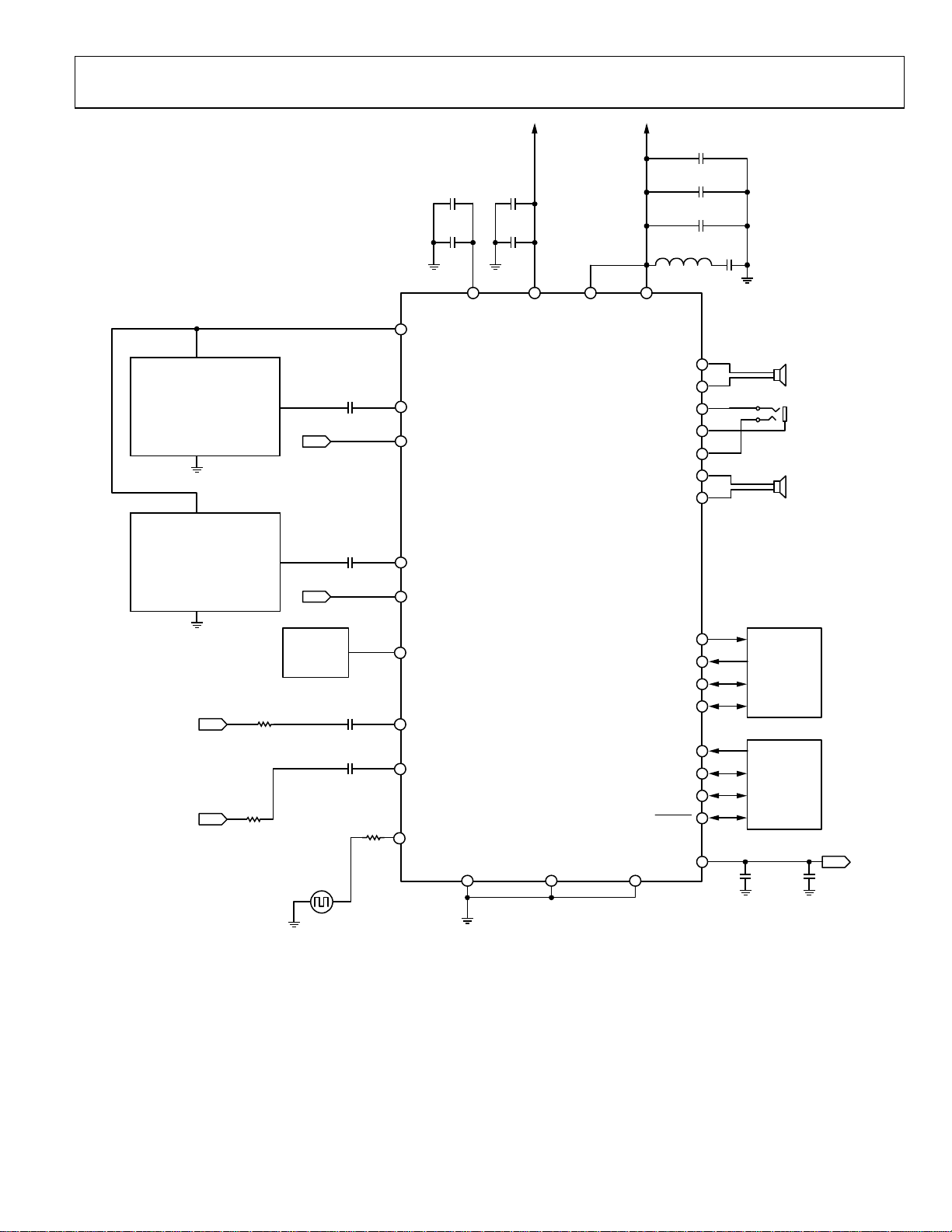
SYSTEM BLOCK DIAGRAMS
10µF
+
1.2nH
LOUTP
LOUTN
RHP
MONOOUT
LHP
ROUTP
ROUTN
0.1µF
0.1µF
9.1pF
EARPIECE
SPEAKER
CAPLESS
HEADPHONE
OUTPUT
EARPIECE
SPEAKER
THE INPUT CAPACI TOR VALUE DE PENDS ON THE
INPUT IMPE DANCE, WHICH VARI ES WITH T HE
VOLUME SETTING.
10µF
LEFT
MICROPHONE
10µF
2k
2k
10µF
10µF 10µ F
0.1µF 0.1µF
LINP
LINN
MICBIAS
++
AVDDIOVDD AVDDDVDDOUT
ADAU1461
RIGHT
MICROPHONE
AUX LEFT
AUX RIGHT
1k
1k
10µF
JACK
DETECTIO N
SIGNAL
CLOCK
SOURCE
10µF
10µF
49.9
RINN
RINP
JACKDET/MICI N
LAUX
RAUX
MCLK
DGND
AGND
Figure 26. System Block Diagram
ADC_SDATA/GPIO 1
DAC_SDATA/GPIO 0
LRCLK/GPI O3
BCLK/GPIO 2
ADDR1/CDATA
SDA/COUT
SCL/CCLK
ADDR0/CLATCH
CM
AGND
0.1µF
SERIAL DATA
SYSTEM
CONTRO LLER
10µF
+
08914-045
Rev. 0 | Page 18 of 88
ADAU1461
10µF
+
1.2nH
0.1µF
0.1µF
9.1pF
THE INPUT CAPACI TOR VALUE DE PENDS ON THE
INPUT IMPE DANCE, WHICH VARI ES WITH T HE
VOLUME SETTING.
MICBIAS
10µF
0.1µF
10µF
++
0.1µF
AVDDIOVDD AVDDDVDDOUT
V
DD
SINGLE-ENDED
ANALOG
MICROPHONE
GND
V
DD
SINGLE-ENDED
ANALOG
MICROPHONE
GND
AUX LEFT
AUX RIGHT
OUTPUT
OUTPUT
1k
1k
CM
CM
JACK
DETECT ION
SIGNAL
CLOCK
SOURCE
10µF
10µF
10µF
10µF
49.9
LINN
LINP
RINN
RINP
JACKDET/MICI N
LAUX
RAUX
MCLK
DGND
ADAU1461
AGND
LOUTP
LOUTN
RHP
MONOOUT
LHP
ROUTP
ROUTN
ADC_SDATA/GPI O1
DAC_SDATA/GPI O0
LRCLK/GPIO3
BCLK/G PIO2
ADDR1/CDATA
SDA/CO UT
SCL/CCLK
ADDR0/CLATCH
CM
AGND
SERIAL DATA
SYSTEM
CONTROLL ER
0.1µF 10µF
EARPIECE
SPEAKER
CAPLESS
HEADPHONE
OUTPUT
EARPIECE
SPEAKER
+
Figure 27. System Block Diagram with Analog Microphones
Rev. 0 | Page 19 of 88
08914-059
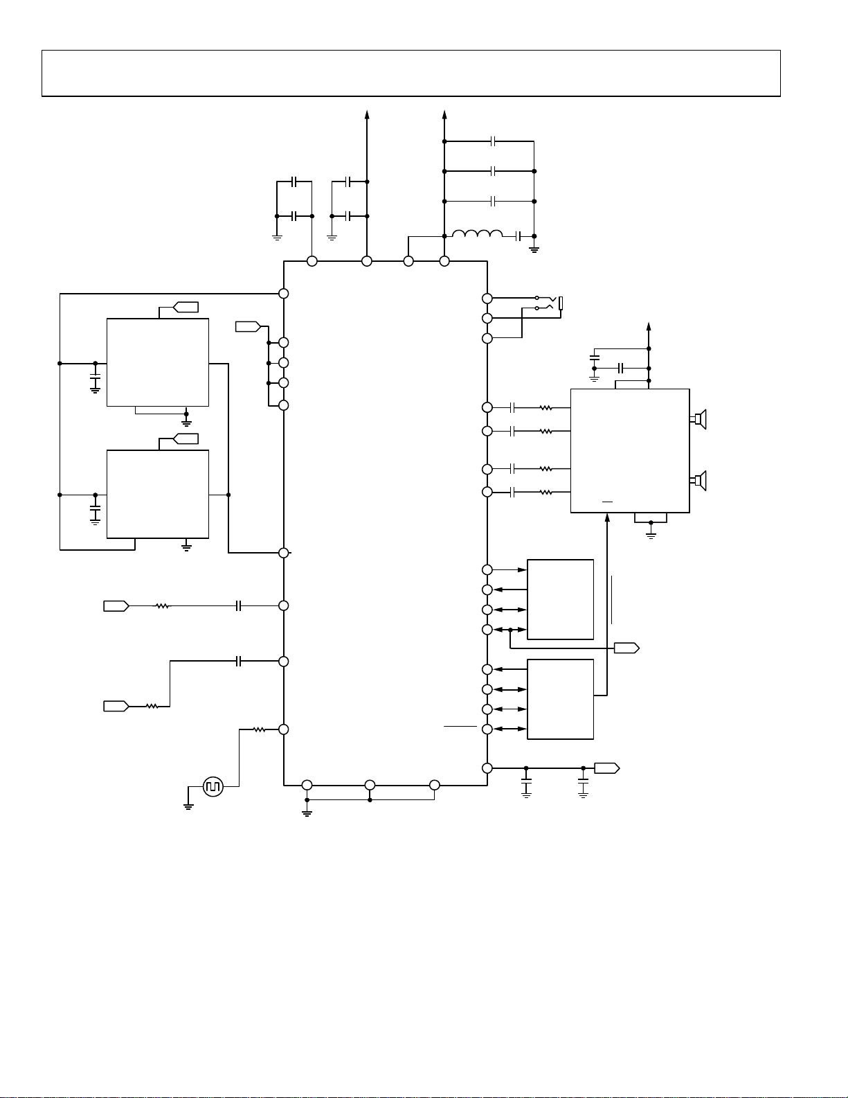
ADAU1461
10µF
+
1.2nH
0.1µF
0.1µF
9.1pF
10µF
0.1µF
10µF
++
0.1µF
0.1µF
0.1µF
V
DD
V
DD
AUX LEFT
AUX RIGHT
CLK
DIGITAL
MICROPHONE
CLK
DIGITAL
MICROPHONE
1k
1k
GNDL/R SELECT
GNDL/R SELECT
DATA
DATA
BCLK
BCLK
CM
10µF
10µF
49.9
MICBIAS
LINP
LINN
RINN
RINP
JACKDET/MICI N
LAUX
RAUX
MCLK
ADAU1461
AVDDIOVDD AVDDDVDDOUT
RHP
MONOOUT
LHP
LOUTP
LOUTN
ROUTP
ROUTN
ADC_SDATA/GPI O1
DAC_SDATA/GPI O0
LRCLK/GPI O3
BCLK/G PIO2
ADDR1/CDATA
SDA/COUT
SCL/CCLK
ADDR0/CLATCH
CAPLESS
HEADPHONE
OUTPUT
22nF
22nF
22nF
22nF
10µF
R
EXT
INL+
R
EXT
INL–
R
EXT
INR+
R
EXT
INR–
SERIAL DATA
SYSTEM
CONTROLL ER
2.5V TO 5.0V
0.1µF
VDDVDD
SSM2306
CLASS-D 2W
STEREO SPEAKER
DRIVER
GNDSD GND
SHUTDOWN
OUTL+
OUTL–
OUTR+
OUTR–
LEFT
SPEAKER
RIGHT
SPEAKER
CLOCK
SOURCE
DGND
AGND
AGND
CM
0.1µF 10µF
+
08914-060
Figure 28. System Block Diagram with Digital Microphones and SSM2306 Class-D Speaker Driver
Rev. 0 | Page 20 of 88

ADAU1461
THEORY OF OPERATION
The ADAU1461 is a low power audio codec with an integrated
stream-oriented DSP core, making it an all-in-one package that
offers high quality audio, low power, small size, and many
advanced features. The stereo ADC and stereo DAC each have
an SNR of at least +98 dB and a THD + N of at least −90 dB.
The serial data port is compatible with I
justified, and TDM modes for interfacing to digital audio data.
The operating voltage is 3.3 V, with an on-board regulator
generating the internal digital supply voltage.
The record signal path includes very flexible input configurations
that can accept differential and single-ended analog microphone
inputs as well as a digital microphone input. A microphone bias
pin provides seamless interfacing to electret microphones. Input
configurations can accept up to six single-ended analog signals
or variations of stereo differential or stereo single-ended signals
with two additional auxiliary single-ended inputs. Each input
signal has its own programmable gain amplifier (PGA) for volume
adjustment and can be routed directly to the playback path output
mixers, bypassing the ADCs. An automatic level control (ALC)
can also be implemented to keep the recording volume constant.
The ADCs and DACs are high quality, 24-bit Σ- converters
that operate at selectable 64× or 128× oversampling ratios. The
base sampling rate of the converters is set by the input clock rate
and can be further scaled with the converter control register
settings. The converters can operate at sampling frequencies
from 8 kHz to 96 kHz. The ADCs and DACs also include very
fine-step digital volume controls.
The playback path allows input signals and DAC outputs to be
mixed into various output configurations. Headphone drivers
are available for a stereo headphone output, and the other output
pins are capable of differentially driving an earpiece speaker.
Capless headphone outputs are possible with the use of the
mono output as a virtual ground connection. The stereo line
outputs can be used as either single-ended or differential
outputs and as an optional mix-down mono output.
The DSP core introduces many features that make this codec
unique and optimized for audio processing. The program and
parameter RAMs can be loaded with custom audio processing
signal flow built using the SigmaStudio graphical programming
software from Analog Devices, Inc. The values stored in the
parameter RAM control individual signal processing blocks,
such as equalization filters, dynamics processors, audio delays,
and mixer levels.
2
S, left-justified, right-
The SigmaStudio software is used to program and control the
SigmaDSP through the control port. Along with designing and
tuning a signal flow, the tools can be used to configure all of the
DSP registers. The SigmaStudio graphical interface allows anyone with digital or analog audio processing knowledge to easily
design DSP signal flow and port it to a target application. At the
same time, it provides enough flexibility and programmability
for an experienced DSP programmer to have in-depth control
of the design. In SigmaStudio, the user can connect graphical
blocks (such as biquad filters, dynamics processors, mixers, and
delays), compile the design, and load the program and parameter
files into the ADAU1461 memory through the control port.
Signal processing blocks available in the provided libraries
include the following:
• Enhanced stereo capture
• Single- and double-precision biquad filters
• FIR filters
• Dynamics processors with peak or rms detection for mono
and multichannel dynamics
• Mixers and splitters
• Tone and noise generators
• Fixed and variable gain
• Loudness
• Delay
• Stereo enhancement
• Dynamic bass boost
• Noise and tone sources
• Level detectors
Additional processing blocks are always being developed.
Analog Devices also provides proprietary and third-party
algorithms for applications such as matrix decoding, bass
enhancement, and surround virtualizers. Contact Analog
Devices (
these algorithms.
The ADAU1461 can generate its internal clocks from a wide
range of input clocks by using the on-board fractional PLL.
The PLL accepts inputs from 8 MHz to 27 MHz.
The ADAU1461 is provided in a small, 32-lead, 5 mm × 5 mm
LFCSP with an exposed bottom pad.
www.analog.com) for information about licensing
Rev. 0 | Page 21 of 88
ADAU1461
STARTUP, INITIALIZATION, AND POWER
This section describes the procedure for properly starting up
the ADAU1461. The following sequence provides a high level
approach to the proper initiation of the system.
1. Apply power to the ADAU1461.
2. Lock the PLL to the input clock (if using the PLL).
3. Enable the core clock.
4. Load the register settings.
See the Startup section for more information about the proper
start-up sequence.
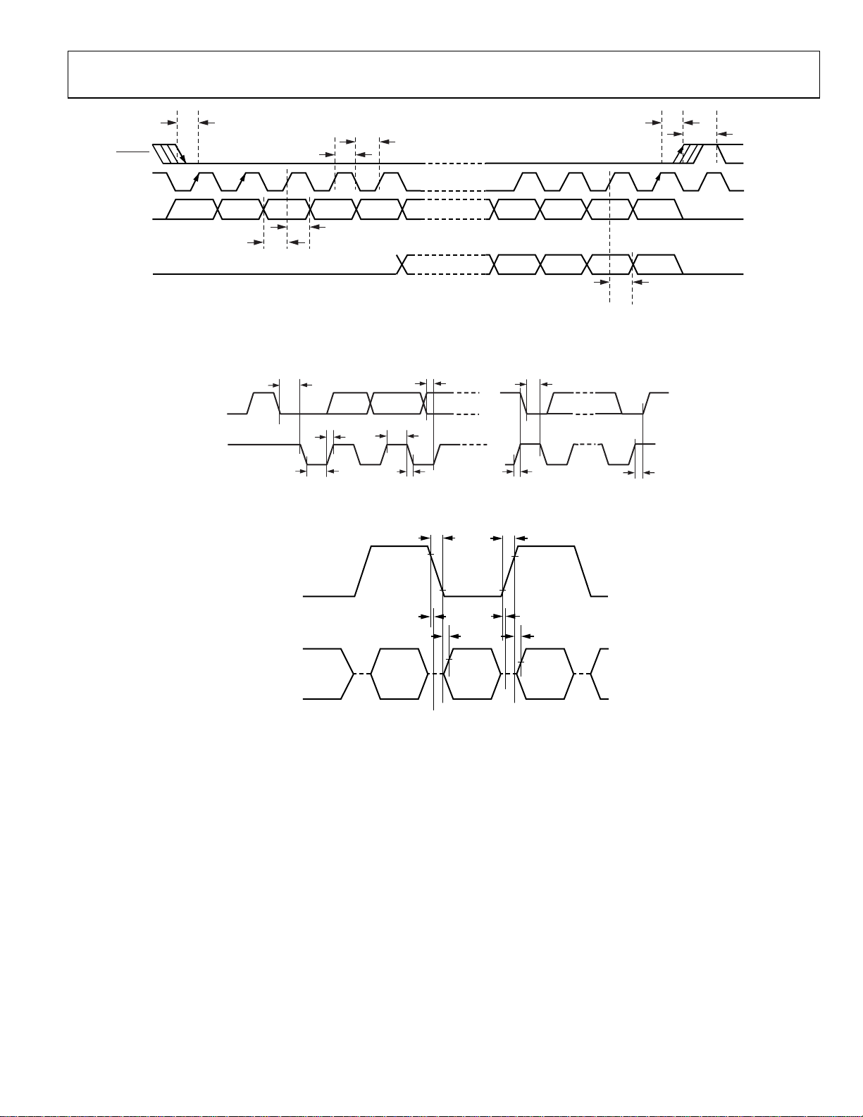
POWER-UP SEQUENCE
The ADAU1461 uses a power-on reset (POR) circuit to
reset the registers upon power-up. The POR monitors the
DVDDOUT pin and generates a reset signal whenever power
is applied to the chip. During the reset, the ADAU1461 is set
to the default values documented in the register map (see the
Control Registers section). Typically, with a 10 F capacitor on
AVDD, the POR takes approximately 14 ms.
1.5V
DVDDOUT
AVDD
POR
POR
ACTIVE
The PLL lock time is dependent on the MCLK rate. Typical
lock times are provided in Tab l e 1 0 . The DSP can be enabled
immediately after the PLL is locked.
Table 10. PLL Lock Times
PLL Mode MCLK Frequency Lock Time (Typical)
Fractional 8 MHz 3.5 ms
Fractional 12 MHz 3.0 ms
Integer 12.288 MHz 2.96 ms
Fractional 13 MHz 2.4 ms
Fractional 14.4 MHz 2.4 ms
Fractional 19.2 MHz 2.98 ms
Fractional 19.68 MHz 2.98 ms
Fractional 19.8 MHz 2.98 ms
Fractional 24 MHz 2.95 ms
Integer 24.576 MHz 2.96 ms
Fractional 26 MHz 2.4 ms
Fractional 27 MHz 2.4 ms
1.35V
PART READY
POR
FINISHED
Figure 29. Power-On Reset Sequence
0.95V
POR ACTIVE
8914-061
POWER REDUCTION MODES
Sections of the ADAU1461 chip can be turned on and off as
needed to reduce power consumption. These include the ADCs,
the DACs, the PLL, and the DSP core.
The digital filters of the ADCs and DACs can each be set to oversampling ratios of 64× or 128× (default). Setting the oversampling
ratios to 64× for these filters lowers power consumption with a
minimal impact on performance. See the Digital Filters section
for specifications; see the Typical Performance Characteristics
section for graphs of these filters.
DIGITAL POWER SUPPLY
The digital power supply for the ADAU1461 is generated from
an internal regulator. This regulator generates a 1.5 V supply
internally. The only external connection to this regulator is the
DVDDOUT bypassing point. A 100 nF capacitor and a 10 F
capacitor should be connected between this pin and DGND.
INPUT/OUTPUT POWER SUPPLY
The power for the digital output pins is supplied from IOVDD,
and this pin also sets the highest input voltage that should be
seen on the digital input pins. IOVDD should be set to 3.3 V; no
digital input signal should be at a voltage level higher than the
one on IOVDD. The current draw of this pin is variable because
it depends on the loads of the digital outputs. IOVDD should be
decoupled to DGND with a 100 nF capacitor and a 10 F
capacitor.
CLOCK GENERATION AND MANAGEMENT
The ADAU1461 uses a flexible clocking scheme that enables the
use of many different input clock rates. The PLL can be bypassed
or used, resulting in two different approaches to clock management. For more information about clocking schemes, PLL
configuration, and sampling rates, see the Clocking and
Sampling Rates section.
Case 1: PLL Is Bypassed
If the PLL is bypassed, the core clock is derived directly from
the MCLK input. The rate of this clock must be set properly in
Register R0 (clock control register, Address 0x4000) using the
INFREQ[1:0] bits. When the PLL is bypassed, supported external
clock rates are 256 × f
is the base sampling rate. The core clock of the chip is off until
the core clock enable bit (COREN) is asserted. If a clock slower
than 1024 × f
is directly input to the ADAU1461 (bypassing the
S
PLL), the number of available SigmaDSP processing cycles is
reduced, and the DSPSR bits in Register R57 (Address 0x40EB)
should be adjusted accordingly.
, 512 × fS, 768 × fS, and 1024 × fS, where fS
S
Rev. 0 | Page 22 of 88

ADAU1461
Case 2: PLL Is Used
The core clock to the entire chip is off during the PLL lock
acquisition period. The user can poll the lock bit to determine
when the PLL has locked. After lock is acquired, the ADAU1461
can be started by asserting the core clock enable bit (COREN)
in Register R0 (clock control register, Address 0x4000). This bit
enables the core clock to all the internal blocks of the ADAU1461.
PLL Lock Acquisition
During the lock acquisition period, only Register R0 (Address
0x4000) and Register R1 (Address 0x4002) are accessible
through the control port. Because all other registers require a
valid master clock for reading and writing, do not attempt to
access any other register. Any read or write is prohibited until
the core clock enable bit (COREN) and the lock bit are both
asserted.
To program the PLL during initialization or reconfiguration of
the clock setting, the following procedure must be followed:
1. Power down the PLL.
2. Reset the PLL control register.
3. Start the PLL.
4. Poll the lock bit.
5. Assert the core clock enable bit after the PLL lock
is acquired.
The PLL control register (Register R1, Address 0x4002) is a
48-bit register where all bits must be written with a single
continuous write to the control port.
Rev. 0 | Page 23 of 88
ADAU1461
G
CLOCKING AND SAMPLING RATES
R1: PLL CONT ROL REGISTER
MCLK
÷ X
× (R + N/M)
CLKSRC
CORE CLOCK
Clocks for the converters, the serial ports, and the DSP are
derived from the core clock. The core clock can be derived
directly from MCLK or it can be generated by the PLL. The
CLKSRC bit (Bit 3 in Register R0, Address 0x4000) determines
the clock source.
The INFREQ[1:0] bits should be set according to the expected
input clock rate selected by CLKSRC; this value also determines
the core clock rate and the base sampling frequency, f
For example, if the input to CLKSRC = 49.152 MHz (from
PLL), then
INFREQ[1:0] = 1024 × f
f
= 49.152 MHz/1024 = 48 kHz
S
The PLL output clock rate is always 1024 × f
control register automatically sets the INFREQ[1:0] bits to
1024 × f
when using the PLL. When using a direct clock, the
S
INFREQ[1:0] frequency should be set according to the MCLK
pin clock rate and the desired base sampling frequency.
S
, and the clock
S
R0: CLOCK
CONTROL REGISTER
INFREQ[1:0]
256 ×
f
768 ×
f
S
Figure 30. Clock Tree Diagram
.
S
, 512 ×
S
, 1024 ×
R57: DSP SAMPLIN
RATE SETTING
DSPSR[3:0]
f
/0.5, 1, 1.5, 2, 3, 4, 6
S
R17: CONVERTER
CORE
CLOCK
f
,
S
f
S
SAMPLING RAT E
CONVSR[2:0]
f
/0.5, 1, 1.5, 2, 3, 4, 6
S
R64: SERIAL PO RT
SAMPLING RAT E
SPSR[2:0]
f
/0.5, 1, 1.5, 2, 3, 4, 6
S
ADC_SDATA/GPI O1
DAC_SDATA/GPI O0
BCLK/GPI O2
LRCLK/GPIO3
ADCs
DACs
SERIAL
DATA INPUT/
OUTPUT PO RT
To utilize the maximum amount of DSP instructions, the core
clock should run at a rate of 1024 × f
.
S
Table 11. Clock Control Register (Register R0, Address 0x4000)
Bits Bit Name Settings
3 CLKSRC
0: Direct from MCLK pin (default)
1: PLL clock
[2:1] INFREQ[1:0]
0 COREN
00: 256 × f
01: 512 × f
10: 768 × f
11: 1024 × f
0: Core clock disabled (default)
(default)
S
S
S
S
1: Core clock enabled
08914-020
Rev. 0 | Page 24 of 88
ADAU1461
SAMPLING RATES
The ADCs, DACs, and serial port share a common sampling
rate that is set in Register R17 (Converter Control 0 register,
Address 0x4017). The CONVSR[2:0] bits set the sampling rate
as a ratio of the base sampling frequency. The DSP sampling
rate is set in Register R57 (DSP sampling rate setting register,
Address 0x40EB) using the DSPSR[3:0] bits, and the serial port
sampling rate is set in Register R64 (serial port sampling rate
register, Address 0x40F8) using the SPSR[2:0] bits.
It is recommended that the sampling rates for the converters,
serial ports, and DSP be set to the same value, unless appropriate
compensation filtering is done within the DSP. Ta b le 1 2 and
Tabl e 13 list the sampling rate divisions for common base
sampling rates.
Table 12. 48 kHz Base Sampling Rate Divisions
Base Sampling
Frequency
fS = 48 kHz fS/1 48 kHz
Table 13. 44.1 kHz Base Sampling Rate Divisions
Base Sampling
Frequency
fS = 44.1 kHz fS/1 44.1 kHz
Sampling Rate Scaling Sampling Rate
fS/6 8 kHz
fS/4 12 kHz
fS/3 16 kHz
fS/2 24 kHz
fS/1.5 32 kHz
fS/0.5 96 kHz
Sampling Rate Scaling Sampling Rate
fS/6 7.35 kHz
fS/4 11.025 kHz
fS/3 14.7 kHz
fS/2 22.05 kHz
fS/1.5 29.4 kHz
fS/0.5 88.2 kHz
PLL
The PLL uses the MCLK as a reference to generate the core
clock. PLL settings are set in Register R1 (PLL control register,
Address 0x4002). Depending on the MCLK frequency, the PLL
must be set for either integer or fractional mode. The PLL can
accept input frequencies in the range of 8 MHz to 27 MHz.
All six bytes in the PLL control register must be written with a
single continuous write to the control port.
TO PLL
MCLK
÷ X
× (R + N/M)
Figure 31. PLL Block Diagram
Integer Mode
Integer mode is used when the MCLK is an integer (R) multiple
of the PLL output (1024 × f
).
S
For example, if MCLK = 12.288 MHz and f
PLL required output = 1024 × 48 kHz = 49.152 MHz
R = 49.152 MHz/12.288 MHz = 4
In integer mode, the values set for N and M are ignored.
Fractional Mode
Fractional mode is used when the MCLK is a fractional
(R + (N/M)) multiple of the PLL output.
For example, if MCLK = 12 MHz and f
PLL required output = 1024 × 48 kHz = 49.152 MHz
R + (N/M) = 49.152 MHz/12 MHz = 4 + (12/125)
Common fractional PLL parameter settings for 44.1 kHz and
48 kHz sampling rates can be found in Table 1 5 and Ta b l e 1 6 .
The PLL outputs a clock in the range of 41 MHz to 54 MHz,
which should be taken into account when calculating PLL
values and MCLK frequencies.
CLOCK DIVIDER
= 48 kHz, then
S
= 48 kHz, then
S
08914-021
Table 14. PLL Control Register (Register R1, Address 0x4002)
Bits Bit Name Description
[47:32] M[15:0] Denominator of the fractional PLL: 16-bit binary number
0x00FD: M = 253 (default)
[31:16] N[15:0] Numerator of the fractional PLL: 16-bit binary number
0x000C: N = 12 (default)
[14:11] R[3:0] Integer part of PLL: four bits, only values 2 to 8 are valid
0010: R = 2 (default)
0011: R = 3
0100: R = 4
0101: R = 5
0110: R = 6
0111: R = 7
1000: R = 8
Rev. 0 | Page 25 of 88
ADAU1461
Bits Bit Name Description
[10:9] X[1:0] PLL input clock divider
00: X = 1 (default)
01: X = 2
10: X = 3
11: X = 4
8 Type PLL operation mode
0: Integer (default)
1: Fractional
1 Lock PLL lock (read-only bit)
0: PLL unlocked (default)
1: PLL locked
0 PLLEN PLL enable
0: PLL disabled (default)
1: PLL enabled
Table 15. Fractional PLL Parameter Settings for f
= 44.1 kHz (PLL Output = 45.1584 MHz = 1024 × fS)
S
MCLK Input (MHz) Input Divider (X) Integer (R) Denominator (M) Numerator (N) R2: PLL Control Setting (Hex)
8 1 5 625 403 0x0271 0193 2901
12 1 3 625 477 0x0271 01DD 1901
13 1 3 8125 3849 0x1FBD 0F09 1901
14.4 2 6 125 34 0x007D 0022 3301
19.2 2 4 125 88 0x007D 0058 2301
19.68 2 4 1025 604 0x0401 025C 2301
19.8 2 4 1375 772 0x055F 0304 2301
24 2 3 625 477 0x0271 01DD 1B01
26 2 3 8125 3849 0x1FBD 0F09 1B01
27 2 3 1875 647 0x0753 0287 1B01
Table 16. Fractional PLL Parameter Settings for f
= 48 kHz (PLL Output = 49.152 MHz = 1024 × fS)
S
MCLK Input (MHz) Input Divider (X) Integer (R) Denominator (M) Numerator (N) R2: PLL Control Setting (Hex)
8 1 6 125 18 0x007D 0012 3101
12 1 4 125 12 0x007D 000C 2101
13 1 3 1625 1269 0x0659 04F5 1901
14.4 2 6 75 62 0x004B 003E 3301
19.2 2 5 25 3 0x0019 0003 2B01
19.68 2 4 205 204 0x00CD 00CC 2301
19.8 2 4 825 796 0x0339 031C 2301
24 2 4 125 12 0x007D 000C 2301
26 2 3 1625 1269 0x0659 04F5 1B01
27 2 3 1125 721 0x0465 02D1 1B01
Table 17. Integer PLL Parameter Settings for f
= 48 kHz (PLL Output = 49.152 MHz = 1024 × fS)
S
MCLK Input (MHz) Input Divider (X) Integer (R) Denominator (M) Numerator (N) R2: PLL Control Setting (Hex)
12.288 1 4 Don’t care Don’t care 0xXXXX XXXX 2001
24.576 1 2 Don’t care Don’t care 0xXXXX XXXX 1001
1
X = don’t care.
Rev. 0 | Page 26 of 88
1
ADAU1461
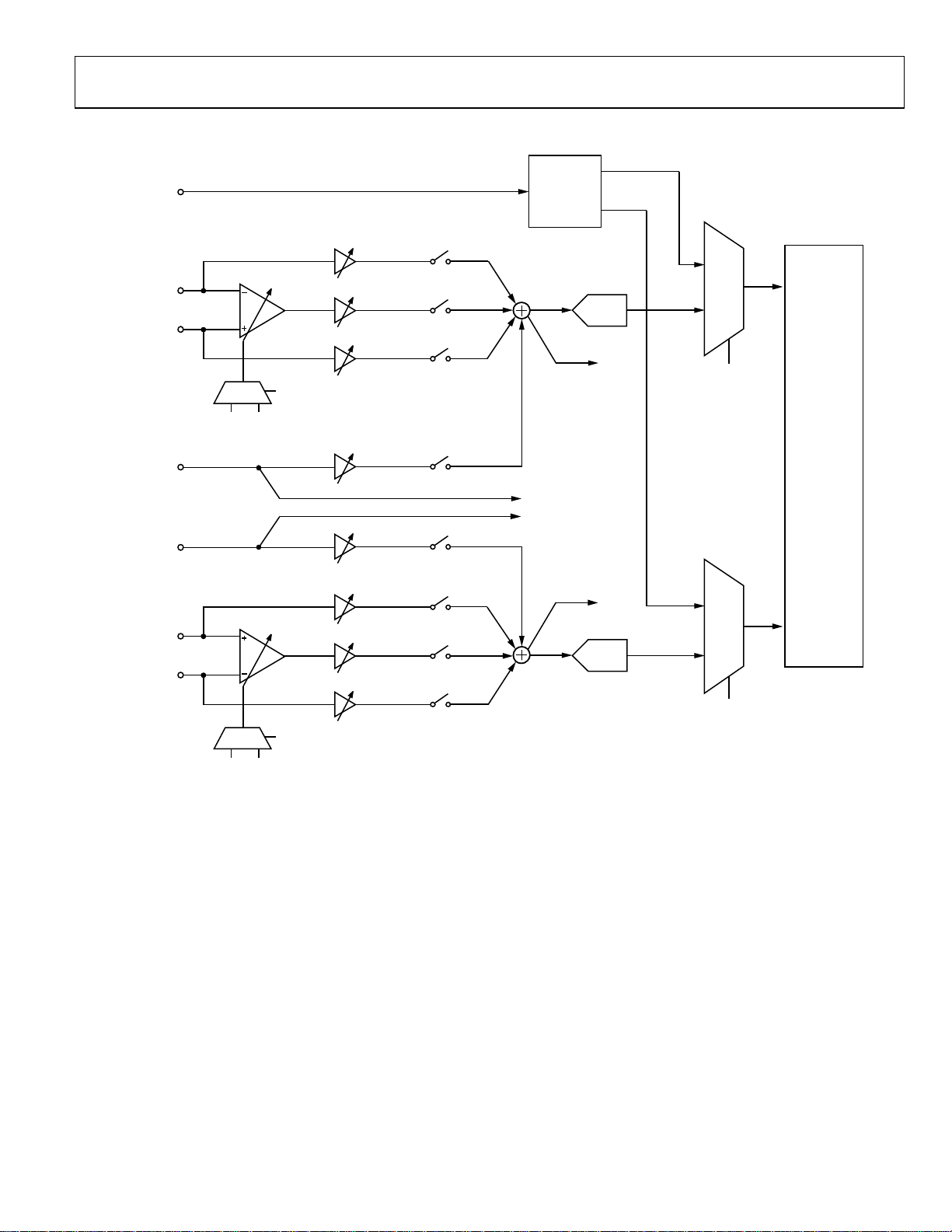
RECORD SIGNAL PATH
MICIN LEF T
DIGITAL
JACKDET/MICI N
LINN
LINP
PGA
–12dB TO
+35.25dB
LINNG[2:0]
–12dB TO +6d B
LDBOOST [1:0]
MUTE/0dB/20dB
LINPG[ 2:0]
MICROPHONE
INTERFACE
MIXER 1
(LEFT RECORD
MIXER)
MICIN RIGHT
LEFT
ADC
–12dB TO +6d B
ALCSEL[2:0]
PGA
ALC
CONTROL
–12dB TO
+35.25dB
ALCSEL[2:0]
ALC
CONTROL
MX1AUXG[2:0]
–12dB TO +6d B
MX2AUXG[2:0]
–12dB TO +6d B
RINPG[2:0]
–12dB TO +6d B
RDBOOST[1: 0]
MUTE/0dB/20dB
RINNG[2:0]
–12dB TO +6d B
LDVOL[5:0]
LAUX
RAUX
RINP
RINN
RDVOL[5:0]
Figure 32. Record Signal Path
INPUT SIGNAL PATHS
The ADAU1461 can accept both line level and microphone
inputs. The analog inputs can be configured in a single-ended
or differential configuration. There is also an input for a digital
microphone. The analog inputs are biased at AVDD/2. Unused
input pins should be connected to CM.
Each of the six analog inputs has individual gain controls (boost
or cut). The input signals are mixed and routed to an ADC. The
mixed input signals can also bypass the ADCs and be routed
directly to the playback mixers. Left channel inputs are mixed
before the left ADC; however, it is possible to route the mixed
analog signal around the ADC and output it into a left or right
output channel. The same capabilities apply to the right channel
and the right ADC.
MIXER 1
OUTPUT
(TO PLAYBACK
MIXER)
AUXILIARY
BYPASS
MIXER 2
OUTPUT
(TO PLAYBACK
MIXER)
MIXER 2
(RIGHT RECORD
MIXER)
RIGHT
ADC
INSEL
INSEL
DECIMATOR/
ALC/
DIGITAL
VOLUME
08914-022
Signals are inverted through the PGAs and the mixers. The
result of this inversion is that differential signals input through
the PGA are output from the ADCs at the same polarity as they
are input. Single-ended inputs that pass through the mixer but
not through the PGA are inverted. The ADCs are noninverting.
The input impedance of the analog inputs varies with the gain
of the PGA. This impedance ranges from 1.7 k at the 35.25 dB
gain setting to 80.4 k at the −12 dB setting. This range is shown
in Figure 25.
Rev. 0 | Page 27 of 88

ADAU1461
Analog Microphone Inputs
For microphone inputs, configure the part in either stereo
pseudo-differential mode or stereo full differential mode.
The LINN and LINP pins are the inverting and noninverting
inputs for the left channel, respectively. The RINN and RINP
pins are the inverting and noninverting inputs for the right
channel, respectively.
For a differential microphone input, connect the positive signal
to the noninverting input of the PGA and the negative signal to
the inverting input of the PGA, as shown in Figure 33. The PGA
settings are controlled with Register R8 (left differential input
volume control register, Address 0x400E) and Register R9 (right
differential input volume control register, Address 0x400F). The
PGA must first be enabled by setting the RDEN and LDEN bits.
ADAU1461
LEFT
LEFT
MICROPHONE
RIGHT
MICROPHONE
2k
2k
LINP
LINN
MICBIAS
RINN
RINP
PGA
RIGHT
PGA
–12dB TO
+35.25dB
–12dB TO
+35.25dB
LDBOOST[1:0]
MUTE/
0dB/20dB
RDBOOST[1:0]
MUTE/
0dB/20dB
08914-052
Figure 33. Stereo Differential Microphone Configuration
The PGA can also be used for single-ended microphone inputs.
Connect LINP and/or RINP to the CM pin. In this configuration, the signal connects to the inverting input of the PGA,
LINN and/or RINN, as shown in Figure 34.
Analog Line Inputs
Line input signals can be accepted by any analog input. It is
possible to route signals on the RINN, RINP, LINN, and LINP
pins around the differential amplifier to their own amplifier and
to use these pins as single-ended line inputs by disabling the
LDEN and RDEN bits (Bit 0 in Register R8, Address 0x400E,
and Bit 0 in Register R9, Address 0x400F). Figure 35 depicts a
stereo single-ended line input using the RINN and LINN pins.
The LAUX and RAUX pins are single-ended line inputs. They
can be used together as a stereo single-ended auxiliary input, as
shown in Figure 35. These inputs can bypass the input gain
control, mixers, and ADCs to directly connect to the output
playback mixers (see auxiliary bypass in Figure 32).
ADAU1461
LINNG[2:0]
LEFT LINE
INPUT
LEFT AUX
INPUT
RIGHT AUX
INPUT
RIGHT LINE
INPUT
Figure 35. Stereo Single-Ended Line Input with Stereo Auxiliary Bypass
LINN
LAUX
RAUX
RINN
–12dB TO +6dB
AUXILIARY
BYPASS
RINNG[2:0]
–12dB TO +6dB
8914-054
LEFT
PGA
LINN
LEFT
MICROPHONE
RIGHT
MICROPHONE
2k
2k
LINP
CM
MICBIAS
RINP
RINN
–12dB TO
+35.25dB
RIGHT
PGA
–12dB TO
+35.25dB
Figure 34. Stereo Single-Ended Microphone Configuration
ADAU1461
LDBOOST [1:0]
MUTE/
0dB/20dB
RDBOOST[1:0]
MUTE/
0dB/20dB
08914-053
Rev. 0 | Page 28 of 88

ADAU1461
Digital Microphone Input Microphone Bias
When using a digital microphone connected to the JACKDET/
MICIN pin, the JDFUNC[1:0] bits in Register R2 (Address 0x4008)
must be set to 10 to enable the microphone input and disable the
jack detection function. The ADAU1461 must operate in master
mode and source BCLK to the input clock of the digital microphone. The DSPRUN bit must also be asserted in Register R62
(DSP run register, Address 0x40F6) for digital microphone
operation.
The digital microphone signal bypasses record path mixers and
ADCs and is routed directly into the decimation filters. The
digital microphone and ADCs share decimation filters and,
therefore, both cannot be used simultaneously. The digital
microphone input select bit, INSEL, can be set in Register R19
(ADC control register, Address 0x4019). Figure 36 depicts the
digital microphone interface and signal routing.
JACKDET/MICI N
R2: DIGITAL MICROPHO NE/
JACK DETECTIO N
CONTRO L
JDFUNC[1:0]
TO JACK
DETECTIO N
CIRCUIT
DIGITAL MICROPHONE
RIGHT
ADC
LEFT
ADC
DECIMATORS
Figure 36. Digital Microphone Interface Block Diagram
INTERFACE
LEFT
CHANNEL
RIGHT
CHANNEL
R19: ADC CONTROL
INSEL
08914-023
The MICBIAS pin provides a voltage reference for electret analog
microphones. The MICBIAS voltage is set in Register R10
(record microphone bias control register, Address 0x4010). In
this register, the MICBIAS output can be enabled or disabled.
Additional options include high performance operation and a
gain boost. The gain boost provides two different voltage biases:
0.65 × AVDD or 0.90 × AVDD. When enabled, the high performance bit increases supply current to the microphone bias
circuit to decrease rms input noise.
The MICBIAS pin can also be used to cleanly supply voltage
to digital microphones or analog microphones with separate
power supply pins.
ANALOG-TO-DIGITAL CONVERTERS
The ADAU1461 uses two 24-bit Σ- analog-to-digital converters (ADCs) with selectable oversampling ratios of 64× or
128× (selected by Bit 3 in Register R17, Address 0x4017).
ADC Full-Scale Level
The full-scale input to the ADCs (0 dBFS) is 1.0 V rms with
AVDD = 3.3 V. This full-scale analog input will output a digital
signal at −1.38 dBFS. This gain offset is built into the ADAU1461
to prevent clipping. The full-scale input level scales linearly with
the level of AVDD.
For single-ended and pseudo-differential signals, the full-scale
value corresponds to the signal level at the pins, 0 dBFS.
The full differential full-scale input level is measured after the
differential amplifier, which corresponds to −6 dBFS at each pin.
Signal levels above the full-scale value cause the ADCs to clip.
Digital ADC Volume Control
The digital ADC volume can be attenuated before DSP processing using Register R20 (left input digital volume register,
Address 0x401A) and Register R21 (right input digital volume
register, Address 0x401B).
High-Pass Filter
By default, a high-pass filter is used in the ADC path to remove
dc offsets; this filter can be enabled or disabled in Register R19
(ADC control register, Address 0x4019). At f
corner frequency of this high-pass filter is 2 Hz.
= 48 kHz, the
S
Rev. 0 | Page 29 of 88
ADAU1461
A
A
AUTOMATIC LEVEL CONTROL (ALC)
The ADAU1461 contains a hardware automatic level control
(ALC). The ALC is designed to continuously adjust the PGA
gain to keep the recording volume constant as the input level
varies.
For optimal noise performance, the ALC uses the analog PGA
to adjust the gain instead of using a digital method. This ensures
that the ADC noise is not amplified at low signal levels.
Extremely small gain step sizes are used to ensure high audio
quality during gain changes.
To use the ALC function, the inputs must be applied either
differentially or pseudo-differentially to input pins LINN and
LINP, for the left channel, and RINN and RINP, for the right
channel. The ALC function is not available for the auxiliary line
input pins, LAUX and RAUX.
A block diagram of the ALC block is shown in Figure 37. The
ALC logic receives the ADC output signals and analyzes these
digital signals to set the PGA gain. The ALC control registers
are used to control the time constants and output levels, as
described in this section.
NALOG
INPUT
LEFT
NALOG
INPUT
RIGHT
I2C
CONTROL
PGA
–12dB TO +35.25dB
0.75dB STEP SIZE
ALC
DIGITAL
Figure 37. ALC Architecture
LEFT
ADC
RIGHT
ADC
MUTE
SERIAL
PORTS
ALC PARAMETERS
The ALC function is controlled with the ALC control registers
(Address 0x4011 through Address 0x4014) using the following
parameters:
• ALCATCK[3:0]: The ALC attack time sets how fast the
ALC starts attenuating after a sudden increase in input
level above the ALC target. Although it may seem that
the attack time should be set as fast as possible to avoid
clipping on transients, using a moderate value results in
better overall sound quality. If the value is too fast, the
ALC overreacts to very short transients, causing audible
gain-pumping effects, which sounds worse than using a
moderate value that allows brief periods of clipping on
transients. A typical setting for music recording is 384 ms.
A typical setting for voice recording is 24 ms.
• ALCHOLD[3:0]: These bits set the ALC hold time. When
the output signal falls below the target output level, the
gain is not increased unless the output remains below the
target level for the period of time set by the hold time bits.
The hold time is used to prevent the gain from modulating
on a steady low frequency sine wave signal, which would
cause distortion.
• ALCDEC[3:0]: The ALC decay time sets how fast the ALC
increases the PGA gain after a sudden decrease in input level
below the ALC target. A very slow setting can be used if the
main function of the ALC is to set a music recording level.
A faster setting can be used if the function of the ALC is to
compress the dynamic range of a voice recording. Using a
very fast decay time can cause audible artifacts such as noise
pumping or distortion. A typical setting for music recording
is 24.58 sec. A typical setting for voice recording is 1.54 sec.
• ALCMAX[2:0]: The maximum ALC gain bits are used to
8914-024
limit the maximum gain that can be programmed into the
ALC. This can be used to prevent excessive noise in the
recording for small input signals. Note that setting this
register to a low value may prevent the ALC from reaching
its target output level, but this behavior is often desirable to
achieve the best overall sound.
• ALCSEL[2:0]: The ALC select bits are used to enable the
ALC and set the mode to left only, right only, stereo, or
DSP. In stereo mode, the greater of the left or right inputs
is used to calculate the gain, and the same gain is then
applied to both the left and right channels. In DSP mode,
the PGA gain is controlled by the SigmaDSP core.
• ALCTARG[3:0]: The ALC target is the desired input
recording level that the ALC attempts to achieve.
Figure 38 shows the dynamic behavior of the PGA gain for a
tone-burst input. The target output is achieved for three different input levels, with the effect of attack, hold, and decay shown
in the figure. Note that for very small signals, the maximum PGA
gain may prevent the ALC from achieving its target level; in the
same way, for very large inputs, the minimum PGA gain may
prevent the ALC from achieving its target level (assuming that
the target output level is set to a very low value). The effects of
the PGA gain limit are shown in the input/output graph of
Figure 39.
Rev. 0 | Page 30 of 88

ADAU1461
the threshold for 250 ms before the noise gate operates.
Hysteresis is used so that the threshold for coming out of the
INPUT
GAIN
OUTPUT
TARGET
DECAY ATTACK
HOLD
TIME TIME
TIME
Figure 38. Basic ALC Operation
MAX GAIN = 30dB
MAX GAIN = 24dB
MAX GAIN = 18dB
MIN PGA
GAIN POINT
mute state is 6 dB higher than the threshold for going into the
mute state. There are four operating modes for the noise gate.
Noise Gate Mode 0 (see Figure 40) is selected by setting the
NGTYP[1:0] bits to 00. In this mode, the current state of the
PGA gain is held at its current state when the noise gate logic is
activated. This prevents a large increase in background noise
during periods of silence. When using this mode, it is advisable
to use a relatively slow decay time. This is because the noise gate
takes at least 250 ms to activate, and if the PGA gain has already
increased to a large value during this time, the value at which
the gain is held will be large.
THRESHOLD
INPUT
08914-025
ANALOG
GAIN
INTERNAL
NOISE GAT E
ENABLE SIGNAL
DIGITAL
MUTE
250ms
GAIN HELD
OUTPUT LEVEL (dB)
INPUT LEVEL (dB)
Figure 39. Effect of Varying the Maximum Gain Parameter
NOISE GATE FUNCTION
When using the ALC, one potential problem is that for small
input signals, the PGA gain can become very large. A side effect
of this is that the noise is amplified along with the signal of
interest. To avoid this situation, the ADAU1461 noise gate can
be used. The noise gate cuts off the ADC output when its signal
level is below a set threshold. The noise gate is controlled using
the following parameters in the ALC Control 3 register
(Address 0x4014):
• NGTYP[1:0]: The noise gate type is set to one of four
modes by writing to the NGTYP[1:0] bits.
• NGEN: The noise gate function is enabled by writing to the
NGEN bit.
• NGTHR[4:0]: The threshold for muting the output is set by
writing to the NGTHR[4:0] bits.
One common problem with noise gate functions is chatter,
where a small signal that is close to the noise gate threshold
varies in amplitude, causing the noise gate function to open and
close rapidly. This causes an unpleasant sound.
To reduce this effect, the noise gate in the ADAU1461 uses a
combination of a timeout period and hysteresis. The timeout
period is set to 250 ms, so the signal must consistently be below
8914-026
OUTPUT
08914-027
Figure 40. Noise Gate Mode 0 (PGA Gain Hold)
Noise Gate Mode 1 (see Figure 41) is selected by setting the
NGTYP[1:0] bits to 01. In this mode, the ADAU1461 does a
simple digital mute of the ADC output. Although this mode
completely eliminates any background noise, the effect of an
abrupt mute may not be pleasant to the ear.
THRESHOLD
INPUT
ANALOG
GAIN
INTERNAL
NOISE GATE
ENABLE SIGNAL
DIGITAL
MUTE
OUTPUT
Figure 41. Noise Gate Mode 1 (Digital Mute)
250ms
08914-028
Rev. 0 | Page 31 of 88
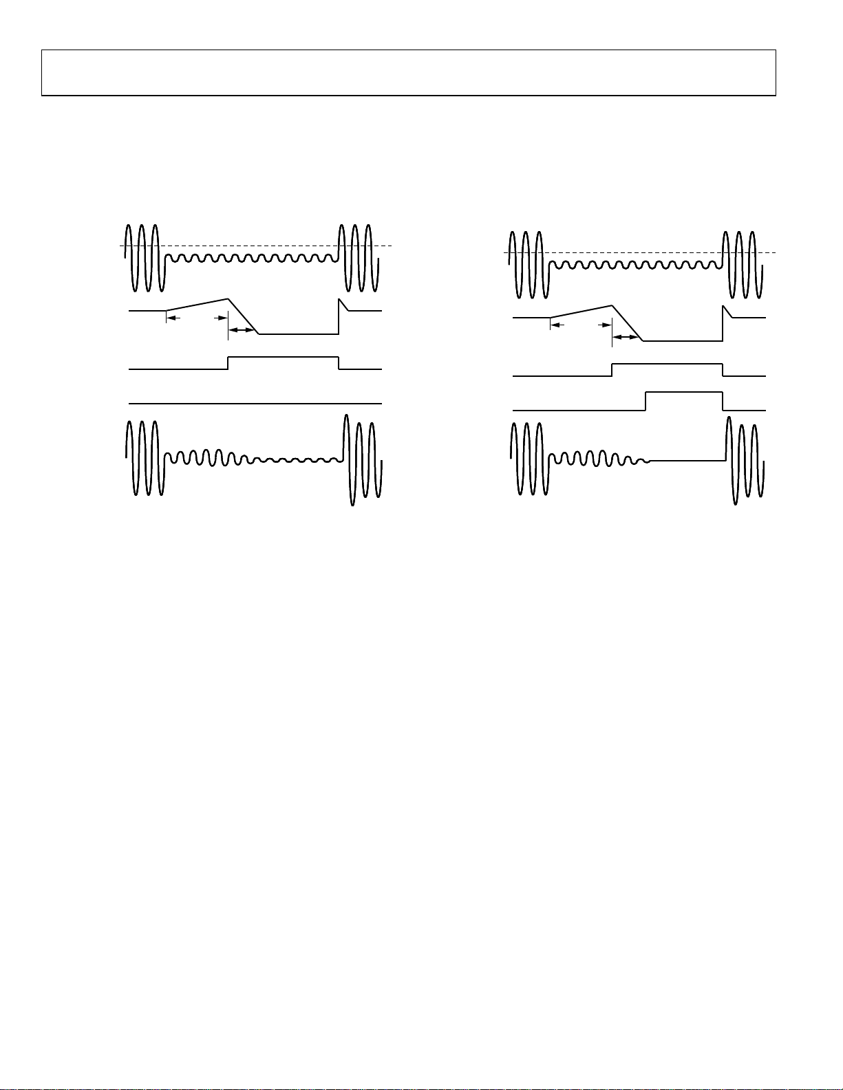
ADAU1461
Noise Gate Mode 2 (see Figure 42) is selected by setting the
NGTYP[1:0] bits to 10. In this mode, the ADAU1461 improves
the sound of the noise gate operation by first fading the PGA
gain over a period of about 100 ms to the minimum PGA gain
value. The ADAU1461 does not do a hard mute after the fade is
complete, so some small background noise will still exist.
THRESHOLD
INPUT
Noise Gate Mode 3 (see Figure 43) is selected by setting the
NGTYP[1:0] bits to 11. This mode is the same as Mode 2 except
that at the end of the PGA fade gain interval, a digital mute is
performed. In general, this mode is the best-sounding mode,
because the audible effect of the digital hard mute is reduced by
the fact that the gain has already faded to a low level before the
mute occurs.
THRESHOLD
INPUT
ANALOG
GAIN
INTERNAL
NOISE GATE
ENABLE SIGNAL
DIGITAL
MUTE
OUTPUT
250ms
100ms
MIN GAIN
Figure 42. Noise Gate Mode 2 (Analog Fade)
08914-029
ANALOG
GAIN
INTERNAL
NOISE GATE
ENABLE SIGNAL
DIGITAL
MUTE
OUTPUT
Figure 43. Noise Gate Mode 3 (Analog Fade/Digital Mute)
250ms
100ms
MIN GAIN
8914-030
Rev. 0 | Page 32 of 88

ADAU1461
R
R
PLAYBACK SIGNAL PATH
MX3G1[3:0]
LEFT INPUT MIXER
RIGHT INPUT MIXE
LAUX
LEFT DAC
RIGHT DAC
LEFT INPUT MIXER
RIGHT INPUT MIXE
RAUX
LEFT DAC
–15dB TO +6dB
MX3G2[3:0]
–15dB TO +6dB
MX3AUXG[3:0]
–15dB TO +6dB
MX4G1[3:0]
–15dB TO +6dB
MX4G2[3:0]
–15dB TO +6dB
MX4AUXG[3:0]
–15dB TO +6dB
MX3LM
MX3RM
MX4LM
MIXER 3
(LEFT
PLAYBACK
MIXER)
MX7[1:0]
MIXER 7
(MONO MIXER)
MIXER 4
(RIGHT
PLAYBACK
MIXER)
MX6G3[1:0]
MX5G4[1:0]
MX5G3[1:0]
MX6G4[1:0]
MIXER 5
(LEFT L/R
PLAYBACK
MIXER)
MIXER 6
(RIGHT L/R
PLAYBACK
MIXER)
LHPVOL[5:0]
–57dB TO +6d B
LOUTVOL[5:0]
–1
MONOVOL [5:0]
–1
ROUTVOL [5:0]
RHPVOL[5:0]
–57dB TO +6d B
–57dB TO +6dB
–57dB TO +6dB
–57dB TO +6d B
LHP
LOUTP
LOUTN
MONOOUT
ROUTN
ROUTP
RHP
RIGHT DAC
MX4RM
Figure 44. Playback Signal Path
OUTPUT SIGNAL PATHS
The outputs of the ADAU1461 can be configured as a variety of
differential or single-ended outputs. All analog output pins are
capable of driving headphone or earpiece speakers. There are
selectable output paths for stereo signals or a downmixed mono
output. The line outputs can drive a load of at least 10 k or can
be put into HP mode to drive headphones or earpiece speakers.
The analog output pins are biased at AVDD/2.
With a 0 dBFS digital input and AVDD = 3.3 V, the full-scale
output level is 920 mV rms.
Signals are inverted through the mixers and volume controls.
The result of this inversion is that the polarity of the differential
outputs and the headphone outputs is preserved. The singleended mono output is inverted. The DACs are noninverting.
08914-031
Routing Flexibility
The playback path contains five mixers (Mixer 3 to Mixer 7)
that perform the following functions:
• Mix signals from the record path and the DACs.
• Mix or swap the left and right channels.
• Mix a mono signal or generate a common-mode output.
Mixer 3 and Mixer 4 are dedicated to mixing signals from the
record path and the DACs. Each of these two mixers can accept
signals from the left and right DACs, the left and right input
mixers, and the dedicated channel auxiliary input. Signals
coming from the record path can be boosted or cut before the
playback mixer.
For example, the MX4G2[3:0] bits set the gain from the output
of Mixer 2 (right record channel) to the input of Mixer 4, hence
the naming convention.
Signals coming from the DACs have digital volume attenuation controls set in Register R20 (left input digital volume
register, Address 0x401A) and Register R21 (right input digital
volume register, Address 0x401B).
Rev. 0 | Page 33 of 88

ADAU1461
HEADPHONE OUTPUT
The LHP and RHP pins can be driven by either a line output
driver or a headphone driver by setting the HPMODE bit in
Register R30 (playback headphone right volume control register,
Address 0x4024). The headphone outputs can drive a load of at
least 16 .
Separate volume controls for the left and right channels range
from −57 dB to +6 dB. Slew can be applied to all the playback
volume controls using the ASLEW[1:0] bits in Register R34
(playback pop/click suppression register, Address 0x4028).
Capless Headphone Configuration
The headphone outputs can be configured in a capless output
configuration with the MONOOUT pin used as a dc virtual
ground reference. Figure 45 depicts a typical playback path in
a capless headphone configuration. Tab l e 1 8 lists the register
settings for this configuration. As shown in this table, the
MONOOUT pin outputs common mode (AVDD/2), which
is used as the virtual headphone reference.
LHPVOL[5:0]
MIXER 3
MX3LM
LEFT
DAC
RIGHT
DAC
Figure 45. Capless Headphone Configuration Diagram
MX7[1:0]
MX4RM
MX3EN
MIXER 7
MX7EN
MIXER 4
MX4EN
MONOM
MOMODE
RHPVOL[5:0]
Table 18. Capless Headphone Register Settings
Register Bit Name Setting
R36 DACEN[1:0] 11 = both DACs on
R22 MX3EN 1 = enable Mixer 3
MX3LM 1 = unmute left DAC input
R24 MX4EN 1 = enable Mixer 4
MX4RM 1 = unmute right DAC input
R28 MX7EN 1 = enable Mixer 7
MX7[1:0] 00 = common-mode output
R33 MONOM 1 = unmute mono output
MOMODE 1 = headphone output
R29 LHPVOL[5:0] Desired volume for LHP output
LHPM 1 = unmute left headphone output
R30 HPMODE 1 = headphone output
RHPVOL[5:0] Desired volume for RHP output
RHPM 1 = unmute right headphone output
LHP
MONOOUT
RHP
08914-062
Headphone Output Power-Up/Power-Down Sequencing
To prevent pops when turning on the headphone outputs, the
user must wait at least 4 ms to unmute these outputs after
enabling the headphone output with the HPMODE bit. This is
because of an internal capacitor that must charge before these
outputs can be used. Figure 46 and Figure 47 illustrate the
headphone power-up/power-down sequencing.
For capless headphones, configure the MONOOUT pin before
unmuting the headphone outputs.
USER
DEFINED
4ms
HPMODE
1 = HEADPHONE
RHPM AND LHPM
1 = UNMUTE
INTERNAL
PRECHARGE
Figure 46. Headphone Output Power-Up Timing
08914-046
RHPM AND LHPM
0 = MUTE
HPMODE
0 = LINE OUTPUT
Figure 47. Headphone Output Power-Down Timing
USER DEFINED
08914-047
Ground-Centered Headphone Configuration
The headphone outputs can also be configured as groundcentered outputs by placing coupling capacitors on the LHP
and RHP pins. Ground-centered headphones should use the
AGND pin as the ground reference.
When the headphone outputs are configured in this manner,
the capacitors create a high-pass filter on the outputs. The
corner frequency of this filter, at which point its attenuation
is 3 dB, is calculated by the following formula:
f
= 1/(2π × R × C)
3dB
where:
C is the capacitor value.
R is the impedance of the headphones.
For a typical headphone impedance of 16 and a 47 F
capacitor, the corner frequency is 211 Hz.
Rev. 0 | Page 34 of 88

ADAU1461
Jack Detection
When the JACKDET/MICIN pin is set to the jack detect function, a flag on this pin can be used to mute the line outputs
when headphones are plugged into the jack. This pin can be
configured in Register R2 (digital microphone/jack detection
control register, Address 0x4008). The JDFUNC[1:0] bits set the
functionality of the JACKDET/MICIN pin.
Additional settings for jack detection include debounce time
(JDDB[1:0] bits) and detection polarity (JDPOL bit). Because
the jack detection and digital microphone share a pin, both
functions cannot be used simultaneously.
POP-AND-CLICK SUPPRESSION
Upon power-up, precharge circuitry is enabled to suppress pops
and clicks. After power-up, the precharge circuitry can be put
into a low power mode using the POPMODE bit in Register R34
(playback pop/click suppression register, Address 0x4028).
The precharge time depends on the capacitor value on the CM
pin and the RC time constant of the load. For a typical line output
load, the precharge time is between 2 ms and 3 ms. After this
precharge time, the POPMODE bit can be set to low power mode.
Changing any register settings that affect the signal path can
cause pops and clicks on the analog outputs. To avoid these pops
and clicks, mute the appropriate outputs using Register R29 to
Register R32 (Address 0x4023 to Address 0x4026). Unmute the
analog outputs after the changes are made.
LINE OUTPUTS
The line output pins (LOUTP, LOUTN, ROUTP, and ROUTN)
can be used to drive both differential and single-ended loads. In
their default settings, these pins can drive typical line loads of
10 k or greater, but they can also be put into headphone mode
by setting the LOMODE bit in Register R31 (playback line output
left volume control register, Address 0x4025) and the ROMODE
bit in Register R32 (playback line output right volume control
register, Address 0x4026). In headphone mode, the line output
pins are capable of driving headphone and earpiece speakers of
16 or greater. The output impedance of the line outputs is
approximately 1 k.
When the line output pins are used in single-ended mode,
LOUTP and ROUTP should be used to output the signals, and
LOUTN and ROUTN should be left unconnected.
The volume controls for these outputs range from −57 dB to
+6 dB. Slew can be applied to all the playback volume controls
using the ASLEW[1:0] bits in Register R34 (playback pop/click
suppression register, Address 0x4028).
The MX5G4[1:0], MX5G3[1:0], MX6G3[1:0], and MX6G4[1:0]
bits can all provide a 6 dB gain boost to the line outputs. This
gain boost allows single-ended output signals to achieve 0 dBV
(1.0 V rms) and differential output signals to achieve up to
6 dBV (2.0 V rms). For more information, see Register R26
(playback L/R mixer left (Mixer 5) line output control register,
Address 0x4020) and Register R27 (playback L/R mixer right
(Mixer 6) line output control register, Address 0x4021).
LEFT DAC
MIXER 3
MX5G3[1:0]
MIXER 5
LOUTVO L[5:0]
LOUTP
RIGHT DAC
–1
–1
MIXER 4
Figure 48. Differential Line Output Configuration
MX6G4[1:0]
MIXER 6
ROUTVO L[5:0]
LOUTN
ROUTN
ROUTP
08914-063
Rev. 0 | Page 35 of 88

ADAU1461
CONTROL PORTS
The ADAU1461 can operate in one of two control modes:
2
C control
• I
• SPI control
The ADAU1461 has both a 4-wire SPI control port and a
2
2-wire I
registers. The part defaults to I
SPI control mode by pulling the
C bus control port. Both ports can be used to set the
2
C mode, but it can be put into
CLATCH
pin low three times.
The control port is capable of full read/write operation for all
addressable registers. The ADAU1461 must have a valid master
clock in order to write to all registers except for Register R0
(Address 0x4000) and Register R1 (Address 0x4002).
All addresses can be accessed in both a single-address mode
or a burst mode. The first byte (Byte 0) of a control port write
contains the 7-bit chip address plus the R/
W
bit. The next two
bytes (Byte 1 and Byte 2) together form the subaddress of the
register location within the ADAU1461. This subaddress must
be two bytes long because the memory locations within the
ADAU1461 are directly addressable and their sizes exceed the
range of single-byte addressing. All subsequent bytes (starting
with Byte 3) contain the data, such as control port data, program
data, or parameter data. The number of bytes per word depends
on the type of data that is being written.
The ADAU1461 has several mechanisms for updating signal processing parameters in real time without causing pops or clicks. If
large blocks of data need to be downloaded, the output of the DSP
core can be halted (using the DSPRUN bit in the DSP run register,
Address 0x40F6), new data can be loaded, and the device can be
restarted. This is typically done during the booting sequence at
start-up or when loading a new program into RAM.
The control port pins are multifunctional, depending on the
mode in which the part is operating. Ta b le 1 9 describes these
multiple functions.
Table 19. Control Port Pin Functions
Pin Name I2C Mode SPI Mode
SCL/CCLK SCL: input clock CCLK: input clock
SDA/COUT
ADDR1/CDATA I2C Address Bit 1: input CDATA: input
ADDR0/CLATCH
SDA: open-collector
input/output
I2C Address Bit 0: input
COUT: output
CLATCH
: input
BURST MODE WRITING AND READING
Burst mode addressing, where the subaddresses are automatically
incremented at word boundaries, can be used for writing large
amounts of data to contiguous registers. This increment happens
automatically after a single-word write or read unless a stop condition is encountered (I
burst write starts like a single-word write, but following the first
data-word, the data-word for the next immediate address can be
written immediately without sending its two-byte address.
2
C) or
CLATCH
is brought high (SPI). A
The registers in the ADAU1461 are one byte wide with the
exception of the PLL control register, which is six bytes wide.
The autoincrement feature knows the word length at each
subaddress, so the subaddress does not need to be specified
manually for each address in a burst write.
The subaddresses are autoincremented by 1 following each read
or write of a data-word, regardless of whether there is a valid register or RAM word at that address. Address holes in the register
map can be written to or read from without consequence. In the
ADAU1461, these address holes exist at Address 0x4001, Address
0x4003 to Address 0x4007, Address 0x402E, Address 0x4032 to
Address 0x4035, Address 0x4037 to Address 0x40BF, Address
0x40C5, Address 0x40CA to Address 0x40CF, Address 0x40D5
to Address 0x40EA, and Address 0x40EC to Address 0x40F1. A
single-byte write to these registers is ignored by the ADAU1461,
and a read returns a single byte 0x00.
I2C PORT
The ADAU1461 supports a 2-wire serial (I2C-compatible)
microprocessor bus driving multiple peripherals. Two pins,
serial data (SDA) and serial clock (SCL), carry information
between the ADAU1461 and the system I
2
In I
C mode, the ADAU1461 is always a slave on the bus,
meaning that it cannot initiate a data transfer. Each slave device
is recognized by a unique address. The address and R/
format is shown in . The address resides in the first
seven bits of the I
Tabl e 20
2
C write. Bits[5:6] of the I2C address for the
ADAU1461 are set by the levels on the ADDR1 and ADDR0
pins. The LSB of the address—the R/
read or write operation. Logic Level 1 corresponds to a read
operation, and Logic Level 0 corresponds to a write operation.
Table 20. ADAU1461 I
Bit 0 Bit 1 Bit 2 Bit 3 Bit 4 Bit 5 Bit 6 Bit 7
0 1 1 1 0 ADDR1 ADDR0
2
C Address and Read/
The SDA and SCL pins should each have a 2 kΩ pull-up resistor
on the line connected to it. The voltage on these signal lines
should not be higher than IOVDD (3.3 V).
Addressing
Initially, each device on the I2C bus is in an idle state and
monitors the SDA and SCL lines for a start condition and
the proper address. The I
2
C master initiates a data transfer by
establishing a start condition, defined by a high-to-low transition
on SDA while SCL remains high. This indicates that an address/
data stream follows. All devices on the bus respond to the start
condition and shift the next eight bits (the 7-bit address plus the
W
R/
bit) MSB first. The device that recognizes the transmitted
address responds by pulling the data line low during the ninth
clock pulse. This ninth bit is known as an acknowledge bit. All
other devices withdraw from the bus at this point and return to
the idle condition.
2
C master controller.
W
W
bit—specifies either a
Write
Byte Format
byte
R/W
Rev. 0 | Page 36 of 88

ADAU1461
The R/W bit determines the direction of the data. A Logic 0 on
the LSB of the first byte means that the master will write information to the peripheral, whereas a Logic 1 means that the
master will read information from the peripheral after writing
the subaddress and repeating the start address. A data transfer
takes place until a stop condition is encountered. A stop
condition occurs when SDA transitions from low to high while
SCL is held high. shows the timing of an I
and shows an I
Figure 50
Figure 49
2
C read.
2
C write,
Stop and start conditions can be detected at any stage during the
data transfer. If these conditions are asserted out of sequence with
normal read and write operations, the ADAU1461 immediately
jumps to the idle condition. During a given SCL high period,
SCL
111
SDA
START BY
MASTER
0
CHIP ADDRESS BYTE
0
FRAME 1
R/W
ADDR0ADDR1
ACK BY
ADAU1461
the user should only issue one start condition, one stop condition,
or a single stop condition followed by a single start condition. If
an invalid subaddress is issued by the user, the ADAU1461 does
not issue an acknowledge and returns to the idle condition.
If the user exceeds the highest subaddress while in autoincrement
mode, one of two actions is taken. In read mode, the ADAU1461
outputs the highest subaddress register contents until the master
device issues a no acknowledge, indicating the end of a read. A
no acknowledge condition is where the SDA line is not pulled
low on the ninth clock pulse on SCL. If the highest subaddress
location is reached while in write mode, the data for the invalid
byte is not loaded into any subaddress register, a no acknowledge
is issued by the ADAU1461, and the part returns to the idle
condition.
ACK BY
FRAME 2
SUBADDRESS BYTE 1
ADAU1461
(CONTINUED)
(CONTINUED)
START BY
MASTER
(CONTINUED)
(CONTINUED)
(CONTINUED)
SCL
SDA
SCL
SDA
0111
SCL
SDA
SCL
FRAME 3
SUBADDRESS BYTE 2
0
FRAME 1
CHIP ADDRESS BYTE
FRAME 3
SUBADDRESS BYTE 2
Figure 49. I
ADDR0ADDR1
ACK BY
ADAU1461
2
C Write to ADAU1461 Clocking
R/W
ACK BY
ADAU1461
ACK BY
ADAU1461
REPEATED
START BY MASTER
FRAME 4
DATA BYTE 1
FRAME 2
SUBADDRESS BYTE 1
0111
FRAME 4
CHIP ADDRESS BYTE
0
ADDR1
ADAU1461
ACK BY
ADAU1461
ADDR0
ACK BY
R/W
ADAU1461
STOP BY
MASTER
ACK BY
08914-032
(CONTINUED)
SDA
FRAME 5
READ DATA BYTE 1
Figure 50. I
ACK BY
MASTER
2
C Read from ADAU1461 Clocking
STOP BY
MASTER
Rev. 0 | Page 37 of 88
8914-033

ADAU1461
I2C Read and Write Operations
Figure 51 shows the format of a single-word write operation.
Every ninth clock pulse, the ADAU1461 issues an acknowledge
by pulling SDA low.
Figure 52 shows the format of a burst mode write sequence. This
figure shows an example of a write to sequential single-byte
registers. The ADAU1461 increments its subaddress register
after every byte because the requested subaddress corresponds
to a register or memory area with a 1-byte word length.
Figure 53 shows the format of a single-word read operation. Note
that the first R/
W
bit is 0, indicating a write operation. This is
because the subaddress still needs to be written to set up the
internal address. After the ADAU1461 acknowledges the receipt
of the subaddress, the master must issue a repeated start command
followed by the chip address byte with the R/
W
bit set to 1 (read).
S
Chip address,
R/W
= 0
AS Subaddress high byte AS Subaddress low byte AS Data Byte 1 P
Figure 51. Single-Word I2C Write Format
S
Chip address,
R/W
= 0
AS
Subaddress
high byte
AS
Subaddress
low byte
AS
Figure 52. Burst Mode I2C Write Format
S
Chip address,
R/W
= 0
AS
Subaddress high
byte
AS
Subaddress low
byte
Figure 53. Single-Word I2C Read Format
S
Chip address,
R/W
= 0
AS
Subaddress
high byte
AS
Subaddress
low byte
Figure 54. Burst Mode I2C Read Format
AS S
This causes the ADAU1461 SDA to reverse and begin driving
data back to the master. The master then responds every ninth
pulse with an acknowledge pulse to the ADAU1461.
Figure 54 shows the format of a burst mode read sequence. This
figure shows an example of a read from sequential single-byte
registers. The ADAU1461 increments its subaddress register
after every byte because the requested subaddress corresponds
to a register or memory area with a 1-byte word length. The
ADAU1461 always decodes the subaddress and sets the autoincrement circuit so that the address increments after the
appropriate number of bytes.
Figure 51 to Figure 54 use the following abbreviations:
S = start bit
P = stop bit
AM = acknowledge by master
AS = acknowledge by slave
Data
Byte 1
AS
Data
Byte 2
AS S
Chip address,
= 1
R/W
AS
AS
Data
Byte 3
Chip address,
= 1
R/W
Data
Byte 1
AM
AS
Data
Byte 4
AS
Data
Byte 2
AS … P
Data
Byte 1
AM … P
P
Rev. 0 | Page 38 of 88
ADAU1461
SPI PORT
By default, the ADAU1461 is in I2C mode, but it can be put into
SPI control mode by pulling
CLATCH
done by performing three dummy writes to the SPI port (the
ADAU1461 does not acknowledge these three writes). Beginning
with the fourth SPI write, data can be written to or read from
the IC. The ADAU1461 can be taken out of SPI mode only by
a full reset initiated by power-cycling the IC.
The SPI port uses a 4-wire interface, consisting of the
CCLK, CDATA, and COUT signals, and it is always a slave port.
CLATCH
The
signal should go low at the beginning of a transaction and high at the end of a transaction. The CCLK signal
latches CDATA on a low-to-high transition. COUT data is shifted
out of the ADAU1461 on the falling edge of CCLK and should
be clocked into a receiving device, such as a microcontroller, on
the CCLK rising edge. The CDATA signal carries the serial input
data, and the COUT signal carries the serial output data. The
COUT signal remains three-state until a read operation is requested.
This allows other SPI-compatible peripherals to share the same
readback line. All SPI transactions have the same basic format
shown in . A timing diagram is shown in . All
Tabl e 22 Figure 4
data should be written MSB first.
low three times. This is
CLATCH
,
Chip Address R/W
The LSB of the first byte of an SPI transaction is a R/W bit. This bit
determines whether the communication is a read (Logic Level 1)
or a write (Logic Level 0). This format is shown in . Table 21
Table 21. ADAU1461 SPI Address and Read/
Write
Byte Format
Bit 0 Bit 1 Bit 2 Bit 3 Bit 4 Bit 5 Bit 6 Bit 7
0 0 0 0 0 0 0
R/W
Subaddress
The 16-bit subaddress word is decoded into a location in one of
the registers. This subaddress is the location of the appropriate
register. The MSBs of the subaddress are zero-padded to bring
the word to a full 2-byte length.
Data Bytes
The number of data bytes varies according to the register being
accessed. During a burst mode write, an initial subaddress is
written followed by a continuous sequence of data for consecutive register locations.
A sample timing diagram for a single-word SPI write operation
to a register is shown in Figure 55. A sample timing diagram of
a single-word SPI read operation is shown in Figure 56. The
COUT pin goes from being three-state to being driven at the
beginning of Byte 3. In this example, Byte 0 to Byte 2 contain
the addresses and R/
W
bit, and subsequent bytes carry the data.
Table 22. Generic Control Word Format
Byte 0 Byte 1 Byte 2 Byte 3 Byte 4
chip_adr[6:0], R/W
1
Continues to end of data.
subaddr[15:8] subaddr[7:0] data data
CLATCH
CCLK
CDATA
BYTE 0 BYTE 1 BYTE 2 BYTE 3
Figure 55. SPI Write to ADAU1461 Clocking (Single-Word Write Mode)
CLATCH
CCLK
CDATA
COUT
BYTE 0
HIGH-Z
Figure 56. SPI Read from ADAU1461 Clocking (Single-Word Read Mode)
BYTE 1
BYTE 2
DATA
HIGH-Z
1
08914-038
08914-039
Rev. 0 | Page 39 of 88

ADAU1461
47pF
SERIAL DATA INPUT/OUTPUT PORTS
The flexible serial data input and output ports of the ADAU1461
can be set to accept or transmit data in 2-channel format or in
a 4-channel or 8-channel TDM stream to interface to external
ADCs or DACs. Data is processed in twos complement, MSB
first format. The left channel data field always precedes the right
channel data field in 2-channel streams. In TDM mode, Slot 0
to Slot 3 are in the first half of the audio frame, and Slot 4 to
Slot 7 are in the second half of the frame. The serial modes and
the position of the data in the frame are set in Register R15 to
Register R18 (serial port and converter control registers,
Address 0x4015 to Address 0x4018).
If the PLL of the ADAU1461 is not used, the serial data clocks
must be synchronous with the ADAU1461 master clock input.
The LRCLK and BCLK pins are used to clock both the serial
input and output ports. The ADAU1461 can be set as the master
or the slave in a system. Because there is only one set of serial
data clocks, the input and output ports must always be both
master or both slave.
Register R15 and Register R16 (serial port control registers,
Address 0x4015 and Address 0x4016) allow control of clock
polarity and data input modes. The valid data formats are I
2
S,
left-justified, right-justified (24-/20-/18-/16-bit), and TDM. In
all modes except for the right-justified modes, the serial port
inputs an arbitrary number of bits up to a limit of 24. Extra bits
do not cause an error, but they are truncated internally.
The serial port can operate with an arbitrary number of BCLK
transitions in each LRCLK frame. The LRCLK in TDM mode
can be input to the ADAU1461 either as a 50% duty cycle clock
or as a bit-wide pulse.
When the LRCLK is set as a pulse, a 47 pF capacitor should be
connected between the LRCLK pin and ground (see Figure 57).
This capacitor is necessary in both master and slave modes to
properly align the LRCLK signal to the serial data stream.
ADAU1461
LRCLK
BCLK
Figure 57. LRCLK Capacitor Alignment, TDM Pulse Mode
08914-071
In TDM 8 mode, the ADAU1461 can be a master for fS up to
48 kHz. Tabl e 23 lists the modes in which the serial output port
can function.
Table 23. Serial Output Port Master/Slave Mode Capabilities
2-Channel Modes (I
fS
48 kHz Master and slave Master and slave
96 kHz Master and slave Slave
Justified, Right-Justified) 8-Channel TDM
2
S, Left-
Tabl e 24 describes the proper configurations for standard audio
data formats.
Table 24. Data Format Configurations
LRCLK Mode
Format LRCLK Polarity (LRPOL)
I2S
(see Figure 58)
Left-Justified (see
Figure 59)
Right-Justified
(see Figure 60)
TDM with Clock
(see Figure 61)
TDM with Pulse
(see Figure 62)
Frame begins on falling edge 50% duty cycle
Frame begins on rising edge 50% duty cycle
Frame begins on rising edge 50% duty cycle
Frame begins on falling edge 50% duty cycle
Frame begins on rising edge Pulse
(LRMOD)
BCLK Polarity
(BPOL)
Data changes
on falling edge
Data changes
on falling edge
Data changes
on falling edge
Data changes
on falling edge
Data changes
on falling edge
BCLK Cycles/Audio
Frame (BPF[2:0])
32 to 64
32 to 64
32 to 64
64 to 256
64 to 256
Data Delay from LRCLK
Edge (LRDEL[1:0])
Delayed from LRCLK edge
by 1 BCLK
Aligned with LRCLK edge
Delayed from LRCLK edge
by 8 or 16 BCLKs
Delayed from start of word
clock by 1 BCLK
Delayed from start of word
clock by 1 BCLK
Rev. 0 | Page 40 of 88

ADAU1461
K
S
A
LRCL
BCLK
SDATA MSB
LRCLK
BCLK
SDATA
MSB LSB MS B LSB
LRCLK
BCLK
SDATA
LEFT CHANNEL
LEFT CHANNEL
Figure 58. I
LSB
1/f
2
S Mode—16 Bits to 24 Bits per Channel
S
1/
f
S
MSB
RIGHT CHANNEL
LSB
RIGHT CHANNE L
Figure 59. Left-Justified Mode—16 Bits to 24 Bits per Channel
LEFT CHANNEL
MSB LSB MSB LSB
1/
f
S
RIGHT CHANNEL
Figure 60. Right-Justified Mode—16 Bits to 24 Bits per Channel
LRCLK
BCLK
DAT
32 BCLKs
SLOT 0 SLOT 3 SLOT 4
SLOT 1 SLOT 2 SLOT 5 SLOT 6 SLOT 7
256 BCLKs
08914-040
8914-041
08914-042
LRCLK
BCLK
MSB MSB – 1 MSB – 2
SDATA
08914-043
Figure 61. TDM 8 Mode
LRCLK
BCLK
SDATA
MSB TDM
CH
0
SLOT 0 SLOT 1 SLOT 2 SLOT 3 SLOT 4 SLOT 5 SLOT 6 SLOT 7
32
BCLKs
MSB TDM
CH
8
08914-044
Figure 62. TDM 8 Mode with Pulse Word Clock
Rev. 0 | Page 41 of 88

ADAU1461
V
A
APPLICATIONS INFORMATION
POWER SUPPLY BYPASS CAPACITORS
Each analog and digital power supply pin should be bypassed to
its nearest appropriate ground pin with a single 100 nF capacitor. The connections to each side of the capacitor should be as
short as possible, and the trace should stay on a single layer with
no vias. For maximum effectiveness, locate the capacitor equidistant from the power and ground pins or, when equidistant
placement is not possible, slightly closer to the power pin.
Thermal connections to the ground planes should be made
on the far side of the capacitor.
Each supply signal on the board should also be bypassed with a
single bulk capacitor (10 F to 47 F).
DD GND
CAPACITOR
TO VDD
TO GND
Figure 63. Recommended Power Supply Bypass Capacitor Layout
08914-048
GSM NOISE FILTER
In mobile phone applications, excessive 217 Hz GSM noise on
the analog supply pins can degrade the audio quality. To avoid
this problem, it is recommended that an L-C filter be used in
series with the bypass capacitors for the AVDD pins. This filter
should consist of a 1.2 nH inductor and a 9.1 pF capacitor in
series between AVDD and ground, as shown in Figure 64.
GROUNDING
A single ground plane should be used in the application layout.
Components in an analog signal path should be placed away
from digital signals.
EXPOSED PAD PCB DESIGN
The ADAU1461 has an exposed pad on the underside of the
LFCSP. This pad is used to couple the package to the PCB for
heat dissipation when using the outputs to drive earpiece or
headphone loads. When designing a board for the ADAU1461,
special consideration should be given to the following:
• A copper layer equal in size to the exposed pad should be
on all layers of the board, from top to bottom, and should
connect somewhere to a dedicated copper board layer (see
Figure 65).
• Vias should be placed to connect all layers of copper,
allowing for efficient heat and energy conductivity. For an
example, see Figure 66, which has nine vias arranged in a
3 inch × 3 inch grid in the pad area.
TOP
GROUND
POWER
BOTTOM
VIAS
Figure 65. Exposed Pad Layout Example, Side View
COPPER SQUARES
8914-050
10µF
+
0.1µF
0.1µF
08914-051
9.1pF1.2nH
49
VDD AVDD
Figure 64. GSM Filter on the Analog Supply Pins
8914-0
Figure 66. Exposed Pad Layout Example, Top View
Rev. 0 | Page 42 of 88
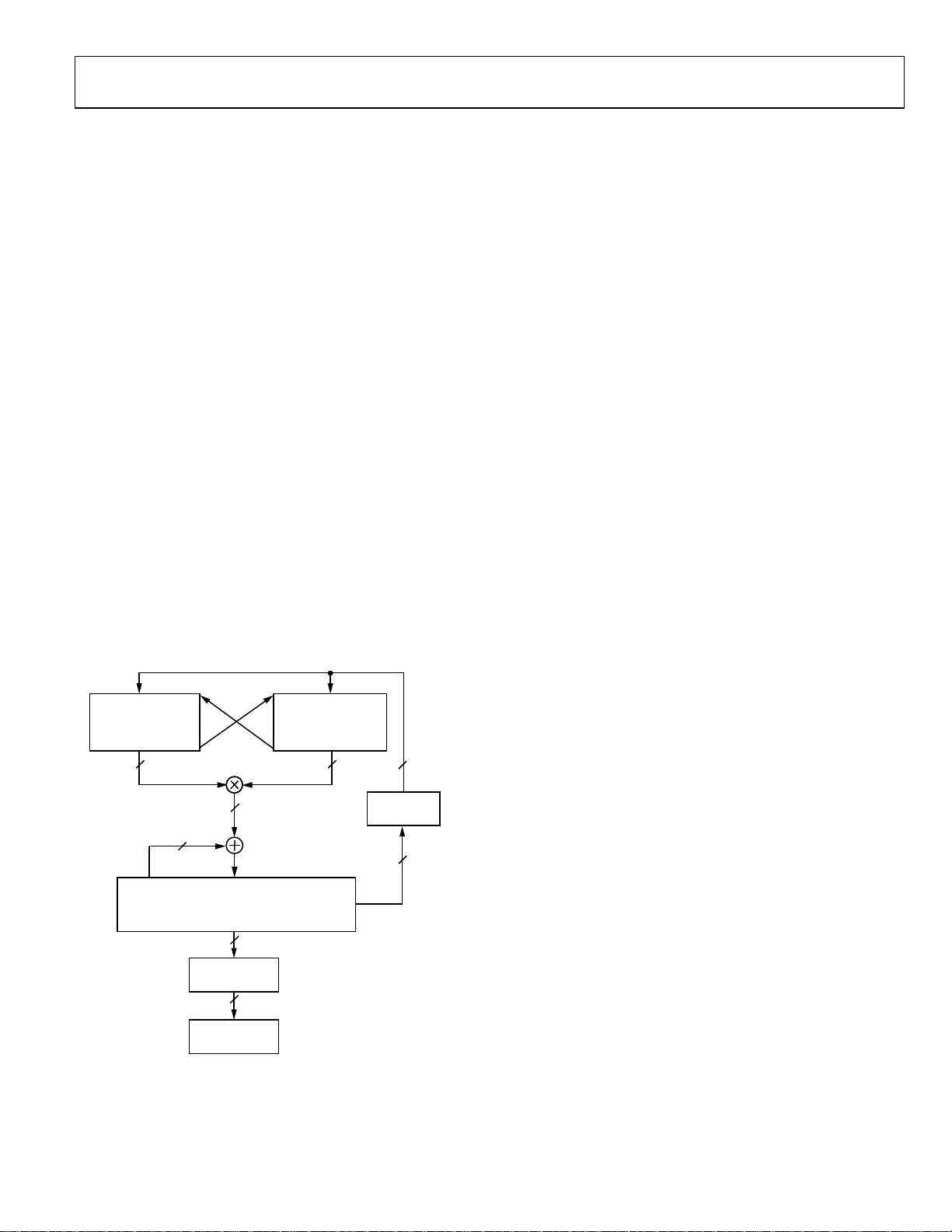
ADAU1461
DSP CORE
SIGNAL PROCESSING
The ADAU1461 is designed to provide all audio signal processing
functions commonly used in stereo or mono low power record
and playback systems. The signal processing flow is designed
using the SigmaStudio software, which allows graphical entry
and real-time control of all signal processing functions.
Many of the signal processing functions are coded using full,
56-bit, double-precision arithmetic data. The input and output
word lengths of the DSP core are 24 bits. Four extra headroom
bits are used in the processor to allow internal gains of up to
24 dB without clipping. Additional gains can be achieved by
initially scaling down the input signal in the DSP signal flow.
ARCHITECTURE
The DSP core consists of a simple 28-/56-bit multiply-accumulate
(MAC) unit with two sources: a data source and a coefficient
source. The data source can come from the data RAM, a ROM
table of commonly used constant values, or the audio inputs to
the core. The coefficient source can come from the parameter
RAM or from a ROM table of commonly used constant values.
The two sources are multiplied in a 28-bit fixed-point multiplier
and then the signal is input to the 56-bit adder; the result is usually
stored in one of three 56-bit accumulator registers. The accumulators can be output from the core (in 28-bit format) or can
optionally be written back into the data or parameter RAMs.
DATA SOURCE
(DATA RAM,
ROM CONSTANTS,
AUDIO INPUTS )
56
(ACCUMULATORS ( 3), dB CONVERS ION,
DATA OPERATI ONS
BIT OPERATORS, BIT SHIFTER, ...)
COEFFICIENT SOURCE
(PARAMETER RAM,
ROM CONSTANT S)
56
56
2828
28
TRUNCATOR
56
PROGRAM COUNTER
The execution of instructions in the core is governed by a program
counter, which sequentially steps through the addresses of the
program RAM. The program counter starts every time that a
new audio frame is clocked into the core. SigmaStudio inserts
a jump-to-start command at the end of every program. The
program counter increments sequentially until it reaches this
command and then jumps to the program start address and
waits for the next audio frame to clock into the core.
FEATURES
The SigmaDSP core was designed specifically for audio processing
and therefore includes several features intended for maximizing
efficiency. These include hardware decibel conversion and audiospecific ROM constants.
STARTUP
Before the DSPRUN bit is set or any settings are written to the
parameter RAM, the DSP core must be enabled by setting the
DSPEN bit in Register R61 (Address 0x40F5).
The following steps should be performed every time that a new
program is loaded to the SigmaDSP core, or any time that the
DSPRUN bit is disabled and reenabled.
1. Set the DSPSR[3:0] bits in Register R57 (Address 0x40EB)
to 1111 (none).
2. Set the DSPRUN bit in Register R62 (Address 0x40F6) to 0.
3. Download the rest of the registers, the program RAM, and
the parameter RAM.
4. Set the DSPRUN bit in Register R62 to 1.
5. Set the DSPSR[3:0] bits in Register R57 to the operational
setting (default value is 0001).
Changing any register setting or RAM can cause pops and
clicks on the analog outputs. To avoid these pops and clicks,
mute the appropriate outputs using Register R29 to Register R32
(Address 0x4023 to Address 0x4026). Unmute the analog outputs after the startup procedure is completed.
TRUNCATOR
28
OUTPUTS
Figure 67. Simplified DSP Core Architecture
08914-067
Rev. 0 | Page 43 of 88

ADAU1461
NUMERIC FORMATS
DSP systems commonly use a standard numeric format.
Fractional numeric systems are specified by an A.B format,
where A is the number of bits to the left of the decimal point
and B is the number of bits to the right of the decimal point.
The ADAU1461 uses numeric format 5.23 for both the
parameter and data values.
Numeric Format 5.23
Linear range: −16.0 to (+16.0 − 1 LSB)
Examples:
1000 0000 0000 0000 0000 0000 0000 = −16.0
1110 0000 0000 0000 0000 0000 0000 = −4.0
1111 1000 0000 0000 0000 0000 0000 = −1.0
1111 1110 0000 0000 0000 0000 0000 = −0.25
1111 1111 0011 0011 0011 0011 0011 = −0.1
1111 1111 1111 1111 1111 1111 1111 = (1 LSB below 0)
0000 0000 0000 0000 0000 0000 0000 = 0
0000 0000 1100 1100 1100 1100 1101 = 0.1
0000 0010 0000 0000 0000 0000 0000 = 0.25
0000 1000 0000 0000 0000 0000 0000 = 1.0
0010 0000 0000 0000 0000 0000 0000 = 4.0
0111 1111 1111 1111 1111 1111 1111 = (16.0 − 1 LSB)
The serial port accepts up to 24 bits on the input and is signextended to the full 28 bits of the DSP core. This allows internal
gains of up to 24 dB without internal clipping.
A digital clipper circuit is used between the output of the DSP
core and the DACs or serial port outputs (see Figure 68). This
circuit clips the top four bits of the signal to produce a 24-bit
output with a range of 1.0 (minus 1 LSB) to −1.0. Figure 68
shows the maximum signal levels at each point in the data flow
in both binary and decibel levels.
4-BIT SIGN EXTENSION
DATA IN
SERIAL
PORT
1.23
(0dB)
Figure 68. Numeric Precision and Clipping Structure
1.23
(0dB)
5.23
(24dB)
SIGNAL
PROCESSING
(5.23 FORMAT)
5.23
(24dB)
DIGITAL
CLIPPER
1.23
(0dB)
PROGRAMMING
On power-up, the ADAU1461 must be configured with a clocking scheme and then loaded with register settings. After the codec
signal path is set up, the DSP core can be programmed. There
are 1024 instruction cycles per audio sample, resulting in an
internal clock rate of 49.152 MHz when f
The part can be programmed easily using SigmaStudio, a graphical
tool provided by Analog Devices (see Figure 69). No knowledge
of writing line-level DSP code is required. More information
about SigmaStudio can be found at www.analog.com.
= 48 kHz.
S
8914-068
8914-069
Figure 69. SigmaStudio Screen Shot
Rev. 0 | Page 44 of 88

ADAU1461
PROGRAM RAM, PARAMETER RAM, AND DATA RAM
Table 25. RAM Map and Read/Write Modes
Memory Size Address Range Read Write Write Modes
Parameter RAM 1024 × 32 0 to 1023 (0x0000 to 0x03FF) Yes Yes Direct, safeload
Program RAM 1024 × 40 2048 to 3071 (0x0800 to 0x0BFF) Yes Yes Direct
Tabl e 25 shows the RAM map (the ADAU1461 register map is
provided in the Control Registers section). The address space
encompasses a set of registers and three RAMs: program,
parameter, and data. The program RAM and parameter RAM
are not initialized on power-up and are in an unknown state
until written to.
PROGRAM RAM
The program RAM contains the 40-bit operation codes that
are executed by the core. The SigmaStudio compiler calculates
maximum instructions per frame for a project and generates an
error when the value exceeds the maximum allowable instructions
per frame based on the sample rate of the signals in the core.
Because the end of a program contains a jump-to-start command,
the unused program RAM space does not need to be filled with
no-operation (NOP) commands.
PARAMETER RAM
The parameter RAM is 32 bits wide and occupies Address 0
to Address 1023. Each parameter is padded with four 0s before
the MSB to extend the 28-bit word to a full 4-byte width. The
data format of the parameter RAM is twos complement, 5.23.
This means that the coefficients can range from +16.0 (minus
1 LSB) to −16.0, with 1.0 represented by the binary word
0000 1000 0000 0000 0000 0000 0000 or by the hexadecimal
word 0x00 0x80 0x00 0x00.
The parameter RAM can be written to directly or with a safeload write. The direct write mode of operation is typically used
during a complete new loading of the RAM using burst mode
addressing to avoid any clicks or pops in the outputs. Note that
this mode can be used during live program execution, but because
there is no handshaking between the core and the control port,
the parameter RAM is unavailable to the DSP core during control
writes, resulting in pops and clicks in the audio stream.
SigmaStudio automatically assigns the first eight positions to
safeload parameters; therefore, project-specific parameters start
at Address 0x0008.
The parameter RAM should not be written to until the DSPEN
bit has been set in Register R61 (Address 0x40F5).
DATA RAM
The ADAU1461 data RAM is used to store audio data-words for
processing, as well as certain run-time parameters. SigmaStudio
provides the data and address information for writing to and
reading from the data RAM.
Rev. 0 | Page 45 of 88
When implementing blocks, such as delays, that require large
amounts of data RAM space, data RAM utilization should be
taken into account. The SigmaDSP core processes delay times
in one-sample increments; therefore, the total pool of delay
available to the user equals 4096 multiplied by the sample
period. For a f
maximum of about 86 ms, where f
rate. In practice, this much data memory is not available to the
user because every block in a design uses a few data memory
locations for its processing. In most DSP programs, this does
not significantly affect the total delay time. The SigmaStudio
compiler manages the data RAM and indicates whether the
number of addresses needed in the design exceeds the maximum number available.
of 48 kHz, the pool of available delay is a
S,DSP
is the DSP core sampling
S,DSP
READ/WRITE DATA FORMATS
The read/write formats of the control port are designed to be
byte oriented to allow for easy programming of common microcontroller chips. To fit into a byte-oriented format, 0s are added
to the data fields before the MSB to extend the data-word to
eight bits. For example, 28-bit words written to the parameter
RAM are preceded by four leading 0s to equal 32 bits (four bytes);
40-bit words written to the program RAM are not preceded by
0s because they are already a full five bytes. These zero-padded
data fields are appended to a 3-byte field consisting of a 7-bit
chip address, a read/write bit, and a 16-bit RAM/register address.
The control port knows how many data bytes to expect based
on the address given in the first three bytes.
The total number of bytes for a single-location write command
can vary from one byte (for a control register write) to five bytes
(for a program RAM write). Burst mode can be used to fill
contiguous register or RAM locations. A burst mode write begins
by writing the address and data of the first RAM or register location
to be written. Rather than ending the control port transaction
(by issuing a stop command in I
CLATCH
would be done in a single-address write, the next data-word
can be written immediately without specifying its address. The
ADAU1461 control port autoincrements the address of each write
even across the boundaries of the different RAMs and registers.
signal high in SPI mode after the data-word), as
and show examples of burst mode writes. Tabl e 27 Ta bl e 29
2
C mode or by bringing the

ADAU1461
Table 26. Parameter RAM Read/Write Format (Single Address)
Byte 0 Byte 1 Byte 2 Byte 3 Bytes[4:6]
chip_adr[6:0], R/W
Table 27. Parameter RAM Block Read/Write Format (Burst Mode)
Byte 0 Byte 1 Byte 2 Byte 3 Bytes[4:6] Bytes[7:10] Bytes[11:14]
chip_adr[6:0], R/W
<—param_adr—> param_adr + 1 param_adr + 2
Table 28. Program RAM Read/Write Format (Single Address)
Byte 0 Byte 1 Byte 2 Bytes[3:7]
chip_adr[6:0], R/W
Table 29. Program RAM Block Read/Write Format (Burst Mode)
Byte 0 Byte 1 Byte 2 Bytes[3:7] Bytes[8:12] Bytes[13:17]
chip_adr[6:0], R/W
<—prog_adr—> prog_adr + 1 prog_adr + 2
SOFTWARE SAFELOAD
To update parameters in real time while avoiding pop and click
noises on the output, the ADAU1461 uses a software safeload
mechanism. The software safeload mechanism enables the
SigmaDSP core to load new parameters into RAM while guaranteeing that the parameters are not in use. This prevents an
undesirable condition where an instruction could execute with
a mix of old and new parameters.
SigmaStudio sets up the necessary code and parameters automatically for new projects. The safeload code, along with other
initialization code, fills the first 39 locations in program RAM.
The first eight parameter RAM locations (Address 0x0000 to
Address 0x0007) are configured by default in SigmaStudio as
described in Ta ble 3 0.
Table 30. Software Safeload Parameter RAM Defaults
Address (Hex) Function
0x0000 Modulo RAM size
0x0001 Safeload Data 1
0x0002 Safeload Data 2
0x0003 Safeload Data 3
0x0004 Safeload Data 4
0x0005 Safeload Data 5
0x0006 Safeload target address (offset of −1)
0x0007 Number of words to write/safeload trigger
Address 0x0000, which controls the modulo RAM size, is set
by SigmaStudio and is based on the dynamic address generator
mode of the project.
param_adr[15:8] param_adr[7:0] 0000, param[27:24] param[23:0]
param_adr[15:8] param_adr[7:0] 0000, param[27:24] param[23:0]
prog_adr[15:8] prog_adr[7:0] prog[39:0]
prog_adr[15:8] prog_adr[7:0] prog[39:0]
Parameter RAM Address 0x0001 to Address 0x0005 are the five
data slots for storing the data to be safeloaded. The safeload
parameter space contains five data slots by default because most
standard signal processing algorithms have five parameters or less.
Address 0x0006 is the target address in parameter RAM (with
an offset of −1). This designates the first address to be written.
If more than one word is written, the address increments automatically for each data-word. Up to five sequential parameter
RAM locations can be updated with safeload during each audio
frame. The target address offset of −1 is used because the write
address is calculated relative to the address of the data, which
starts at Address 0x0001. Therefore, to update a parameter at
Address 0x000A, the target address is 0x0009.
Address 0x0007 designates the number of words to be written
into the parameter RAM during the safeload. A biquad filter
uses all five safeload data addresses. A simple mono gain cell
uses only one safeload data address. Writing to Address 0x0007
also triggers the safeload write to occur in the next audio frame.
The safeload mechanism is software based and executes once
per audio frame. Therefore, system designers must take care
when designing the communication protocol. A delay equal to
or greater than the sampling period (the inverse of sampling
frequency) is required between each safeload write. A sample
rate of 48 kHz equates to a delay of at least 21 s. If this delay
is not observed, the downloaded data is corrupted.
Rev. 0 | Page 46 of 88

ADAU1461
V
SOFTWARE SLEW
When the values of signal processing parameters are changed
abruptly in real time, they sometimes cause pop and click
sounds to appear on the audio outputs. To avoid pops and
clicks, some algorithms in SigmaStudio implement a software
slew functionality. Algorithms using software slew set a target
value for a parameter and continuously update the value of that
parameter until it reaches the target.
The target value takes an additional space in parameter RAM,
and the current value of the parameter is updated in the nonmodulo section of data RAM. Assignment of parameters and
nonmodulo data RAM is handled by the SigmaStudio compiler
and does not need to be programmed manually.
Slew parameters can follow several different curves, including
an RC-type curve and a linear curve. These curve types are
coded into each algorithm and cannot be modified by the user.
Because algorithms that use software slew generally require more
RAM than their nonslew equivalents, they should be used only
in situations where a parameter will change during operation of
the device.
Figure 70 shows an example of volume slew applied to a sine wave.
SLEW
CURVE
08914-070
INITIAL
ALUE
NEW TARGET
VALUE
Figure 70. Example of Volume Slew
Rev. 0 | Page 47 of 88

ADAU1461
GENERAL-PURPOSE INPUT/OUTPUT
The serial data input/output pins (Pin 26 to Pin 29) are shared
with the general-purpose input/output function. Each of these
four pins can be set to only one of these functions. The function
of these pins is set in the serial data/GPIO pin configuration
register (Register R60, Address 0x40F4).
The GPIOx pins can be used as inputs or outputs. These pins
are readable and can be set through the control port or directly
by the SigmaDSP core. When configured as inputs, the GPIOx
pins can be used with push-button switches or rotary encoders
to control DSP program settings. These pins can also be used
with digital outputs to drive LEDs or external logic to indicate
the status of internal signals and control other devices. Examples
of this use include indicating signal overload, signal present,
and button press confirmation.
When configured as an output, each GPIO pin can typically
drive 2 mA, which is enough current to directly drive some
high efficiency LEDs. Standard LEDs require about 20 mA of
current and can be driven from a GPIO output with an external
transistor or buffer. Because of problems that can arise from
simultaneously driving or sinking a large amount of current on
many pins, avoid connecting high efficiency LEDs directly to
many or all of the GPIO pins when designing the application.
If many LEDs are required, use an external driver. When the
GPIO pins are configured as open-collector outputs, they
should be pulled up to a maximum voltage equal to the voltage
set on IOVDD.
The configuration of the GPIO functions is set up in the
GPIO pin control registers (Register R48 to Register R51,
Address 0x40C6 to Address 0x40C9).
GPIO PINS SET FROM THE CONTROL PORT
The GPIO pins can also be configured to be directly controlled
from the I
mode, four memory locations are enabled for the GPIO pin
settings. The physical settings on the GPIO pins mirror the
settings of the LSB of these 4-byte-wide memory locations.
Table 31. GPIOx Pin Memory Settings (Set from Control Port)
Decimal Hex Bits[31:1] Bit 0
1568 0x0620 Reserved GPIO0SET
1569 0x0621 Reserved GPIO1SET
1570 0x0622 Reserved GPIO2SET
1571 0x0623 Reserved GPIO3SET
2
C/SPI control port. When the pins are set to this
Memory Location
Rev. 0 | Page 48 of 88

ADAU1461
CONTROL REGISTERS
Table 32. Register Map
Reg Address Name Bit 7 Bit 6 Bit 5 Bit 4 Bit 3 Bit 2 Bit 1 Bit 0 Default
R0 0x4000 Clock control Reserved CLKSRC INFREQ[1:0] COREN 00000000
R1 0x4002 PLL control M[15:8] 00000000
M[7:0] 11111101
N[15:8] 00000000
N[7:0] 00001100
Reserved R[3:0] X[1:0] Type 00010000
Reserved Lock PLLEN 00000000
R2 0x4008 Dig mic/jack detect JDDB[1:0] JDFUNC[1:0] Reserved JDPOL 00000000
R3 0x4009 Reserved Reserved 00000000
R4 0x400A Rec Mixer Left 0 Reserved LINPG[2:0] LINNG[2:0] MX1EN 00000000
R5 0x400B Rec Mixer Left 1 Reserved LDBOOST[1:0] MX1AUXG[2:0] 00000000
R6 0x400C Rec Mixer Right 0 Reserved RINPG[2:0] RINNG[2:0] MX2EN 00000000
R7 0x400D Rec Mixer Right 1 Reserved RDBOOST[1:0] MX2AUXG[2:0] 00000000
R8 0x400E Left diff input vol LDVOL[5:0] LDMUTE LDEN 00000000
R9 0x400F Right diff input vol RDVOL[5:0] RDMUTE RDEN 00000000
R10 0x4010 Record mic bias Reserved MPERF MBI Reserved MBIEN 00000000
R11 0x4011 ALC 0 PGASLEW[1:0] ALCMAX[2:0] ALCSEL[2:0] 00000000
R12 0x4012 ALC 1 ALCHOLD[3:0] ALCTARG[3:0] 00000000
R13 0x4013 ALC 2 ALCATCK[3:0] ALCDEC[3:0] 00000000
R14 0x4014 ALC 3 NGTYP[1:0] NGEN NGTHR[4:0] 00000000
R15 0x4015 Serial Port 0 Reserved SPSRS LRMOD BPOL LRPOL CHPF[1:0] MS 00000000
R16 0x4016 Serial Port 1 BPF[2:0] ADTDM DATDM MSBP LRDEL[1:0] 00000000
R17 0x4017 Converter 0 Reserved DAPAIR[1:0] DAOSR ADOSR CONVSR[2:0] 00000000
R18 0x4018 Converter 1 Reserved ADPAIR[1:0] 00000000
R19 0x4019 ADC control Reserved ADCPOL HPF DMPOL DMSW INSEL ADCEN[1:0] 00010000
R20 0x401A Left digital vol LADVOL[7:0] 00000000
R21 0x401B Right digital vol RADVOL[7:0] 00000000
R22 0x401C Play Mixer Left 0 Reserved MX3RM MX3LM MX3AUXG[3:0] MX3EN 00000000
R23 0x401D Play Mixer Left 1 MX3G2[3:0] MX3G1[3:0] 00000000
R24 0x401E Play Mixer Right 0 Reserved MX4RM MX4LM MX4AUXG[3:0] MX4EN 00000000
R25 0x401F Play Mixer Right 1 MX4G2[3:0] MX4G1[3:0] 00000000
R26 0x4020 Play L/R mixer left Reserved MX5G4[1:0] MX5G3[1:0] MX5EN 00000000
R27 0x4021 Play L/R mixer right Reserved MX6G4[1:0] MX6G3[1:0] MX6EN 00000000
R28 0x4022 Play L/R mixer mono Reserved MX7[1:0] MX7EN 00000000
R29 0x4023 Play HP left vol LHPVOL[5:0] LHPM HPEN 00000010
R30 0x4024 Play HP right vol RHPVOL[5:0] RHPM HPMODE 00000010
R31 0x4025 Line output left vol LOUTVOL[5:0] LOUTM LOMODE 00000010
R32 0x4026 Line output right vol ROUTVOL[5:0] ROUTM ROMODE 00000010
R33 0x4027 Play mono output MONOVOL[5:0] MONOM MOMODE 00000010
R34 0x4028 Pop/click suppress Reserved POPMODE POPLESS ASLEW[1:0] Reserved 00000000
R35 0x4029 Play power mgmt Reserved PREN PLEN 00000000
R36 0x402A DAC Control 0 DACMONO[1:0] DACPOL Reserved DEMPH DACEN[1:0] 00000000
R37 0x402B DAC Control 1 LDAVOL[7:0] 00000000
R38 0x402C DAC Control 2 RDAVOL[7:0] 00000000
R39 0x402D Serial port pad ADCSDP[1:0] DACSDP[1:0] LRCLKP[1:0] BCLKP[1:0] 10101010
R40 0x402F Control Port Pad 0 CDATP[1:0] CLCHP[1:0] SCLP[1:0] SDAP[1:0] 10101010
R41 0x4030 Control Port Pad 1 Reserved SDASTR 00000000
R42 0x4031 Jack detect pin Reserved JDSTR Reserved JDP[1:0] Reserved 00001000
R67 0x4036 Dejitter control DEJIT[7:0] 00000011
R43 0x40C0 Cyclic redundancy
R44 0x40C1 CRC[23:16] 00000000
R45 0x40C2 CRC[15:8] 00000000
R46 0x40C3 CRC[7:0] 00000000
check
Rev. 0 | Page 49 of 88
CRC[31:24] 00000000

ADAU1461
Reg Address Name Bit 7 Bit 6 Bit 5 Bit 4 Bit 3 Bit 2 Bit 1 Bit 0 Default
R47 0x40C4 CRC enable Reserved CRCEN 00000000
R48 0x40C6 GPIO0 pin control Reserved GPIO0[3:0] 00000000
R49 0x40C7 GPIO1 pin control Reserved GPIO1[3:0] 00000000
R50 0x40C8 GPIO2 pin control Reserved GPIO2[3:0] 00000000
R51 0x40C9 GPIO3 pin control Reserved GPIO3[3:0] 00000000
R52 0x40D0 Watchdog enable Reserved DOGEN 00000000
R53 0x40D1 Watchdog value DOG[23:16] 00000000
R54 0x40D2 DOG[15:8] 00000000
R55 0x40D3 DOG[7:0] 00000000
R56 0x40D4 Watchdog error Reserved DOGER 00000000
R57 0x40EB DSP sampling rate
setting
R58 0x40F2 Serial input route
control
R59 0x40F3 Serial output route
control
R60 0x40F4 Serial data/GPIO
pin configuration
R61 0x40F5 DSP enable Reserved DSPEN 00000000
R62 0x40F6 DSP run Reserved DSPRUN 00000000
R63 0x40F7 DSP slew modes Reserved MOSLW ROSLW LOSLW RHPSLW LHPSLW 00000000
R64 0x40F8 Serial port
sampling rate
R65 0x40F9 Clock Enable 0 Reserved SLEWPD ALCPD DECPD SOUTPD INTPD SINPD SPPD 00000000
R66 0x40FA Clock Enable 1 Reserved CLK1 CLK0 00000000
Reserved DSPSR[3:0] 00000001
Reserved SINRT[3:0] 00000000
Reserved SOUTRT[3:0] 00000000
Reserved LRGP3 BGP2 SDOGP1 SDIGP0 00000000
Reserved SPSR[2:0] 00000000
CONTROL REGISTER DETAILS
All registers except for the PLL control register are 1-byte write and read registers.
R0: Clock Control, 16,384 (0x4000)
Bit 7 Bit 6 Bit 5 Bit 4 Bit 3 Bit 2 Bit 1 Bit 0
Reserved CLKSRC INFREQ[1:0] COREN
Table 33. Clock Control Register
Bits Bit Name Description
3 CLKSRC
[2:1] INFREQ[1:0]
00 256 × fS (default)
01 512 × fS
10 768 × fS
11 1024 × fS
0 COREN
Clock source select.
0 = direct from MCLK pin (default).
1 = PLL clock.
Input clock frequency. Sets the core clock rate that generates the core clock. If the PLL is used, this value is
automatically set to 1024 × f
.
S
Setting Input Clock Frequency
Core clock enable. Only the R0 and R1 registers can be accessed when this bit is set to 0 (core clock disabled).
0 = core clock disabled (default).
1 = core clock enabled.
Rev. 0 | Page 50 of 88

ADAU1461
R1: PLL Control, 16,386 (0x4002)
Byte Bit 7 Bit 6 Bit 5 Bit 4 Bit 3 Bit 2 Bit 1 Bit 0
0 M[15:8]
1 M[7:0]
2 N[15:8]
3 N[7:0]
4 Reserved R[3:0] X[1:0] Type
5 Reserved Lock PLLEN
Table 34. PLL Control Register
Byte Bits Bit Name Description
0 [7:0] M[15:8] PLL denominator MSB. This value is concatenated with M[7:0] to make up a 16-bit number.
1 [7:0] M[7:0] PLL denominator LSB. This value is concatenated with M[15:8] to make up a 16-bit number.
00000000 00000000 0
… … …
00000000 11111101 253 (default)
… … …
11111111 11111111 65,535
2 [7:0] N[15:8] PLL numerator MSB. This value is concatenated with N[7:0] to make up a 16-bit number.
3 [7:0] N[7:0] PLL numerator LSB. This value is concatenated with N[15:8] to make up a 16-bit number.
00000000 00000000 0
… … …
00000000 00001100 12 (default)
… … …
11111111 11111111 65,535
4 [6:3] R[3:0] PLL integer setting.
0010 2 (default)
0011 3
0100 4
0101 5
0110 6
0111 7
1000 8
4 [2:1] X[1:0] PLL input clock divider.
00 1 (default)
01 2
10 3
11 4
4 0 Type Type of PLL. When set to integer mode, the values of M and N are ignored.
5 1 Lock PLL lock. This read-only bit is flagged when the PLL has finished locking.
5 0 PLLEN
M[15:8] (MSB) M[7:0] (LSB) Value of M
N[15:8] (MSB) N[7:0] (LSB) Value of N
Setting Value of R
Setting Value of X
0 = integer (default).
1 = fractional.
0 = PLL unlocked (default).
1 = PLL locked.
PLL enable.
0 = PLL disabled (default).
1 = PLL enabled.
Rev. 0 | Page 51 of 88

ADAU1461
R2: Digital Microphone/Jack Detection Control, 16,392 (0x4008)
Bit 7 Bit 6 Bit 5 Bit 4 Bit 3 Bit 2 Bit 1 Bit 0
JDDB[1:0] JDFUNC[1:0] Reserved JDPOL
Table 35. Digital Microphone/Jack Detection Control Register
Bits Bit Name Description
[7:6] JDDB[1:0] Jack detect debounce time.
00 5 ms (default)
01 10 ms
10
11
[5:4] JDFUNC[1:0]
00 Jack detect off (default)
01 Jack detect on
10
11
0 JDPOL Jack detect polarity. Detects high or low signal.
R4: Record Mixer Left (Mixer 1) Control 0, 16,394 (0x400A)
This register controls the gain of single-ended inputs for the left channel record path. The left channel record mixer is referred to as Mixer 1.
Bit 7 Bit 6 Bit 5 Bit 4 Bit 3 Bit 2 Bit 1 Bit 0
Reserved LINPG[2:0] LINNG[2:0] MX1EN
Setting Debounce Time
20 ms
40 ms
JACKDET/MICIN pin function. Enables or disables the jack detect function or configures the pin for a digital
microphone input.
Setting Pin Function
Digital microphone input
Reserved
0 = detect high signal (default).
1 = detect low signal.
Table 36. Record Mixer Left (Mixer 1) Control 0 Register
Bits Bit Name Description
[6:4] LINPG[2:0] Gain for a left channel single-ended input from the LINP pin, input to Mixer 1.
Setting Gain
000 Mute (default)
001 −12 dB
010
011
100
101
110
111
−9 dB
−6 dB
−3 dB
0 dB
3 dB
6 dB
[3:1] LINNG[2:0] Gain for a left channel single-ended input from the LINN pin, input to Mixer 1.
Setting Gain
000 Mute (default)
001 −12 dB
010
011
100
101
110
111
−9 dB
−6 dB
−3 dB
0 dB
3 dB
6 dB
0 MX1EN Left channel mixer enable in the record path. Referred to as Mixer 1.
0 = mixer disabled (default).
1 = mixer enabled.
Rev. 0 | Page 52 of 88

ADAU1461
R5: Record Mixer Left (Mixer 1) Control 1, 16,395 (0x400B)
This register controls the gain boost of the left channel differential PGA input and the gain for the left channel auxiliary input in the
record path. The left channel record mixer is referred to as Mixer 1.
Bit 7 Bit 6 Bit 5 Bit 4 Bit 3 Bit 2 Bit 1 Bit 0
Reserved
Table 37. Record Mixer Left (Mixer 1) Control 1 Register
Bits Bit Name Description
[4:3] LDBOOST[1:0]
00 Mute (default)
01 0 dB
10
11
[2:0] MX1AUXG[2:0] Left single-ended auxiliary input gain from the LAUX pin in the record path, input to Mixer 1.
000 Mute (default)
001 −12 dB
010
011
100
101
110
111 6 dB
Left channel differential PGA input gain boost, input to Mixer 1. The left differential input uses the LINP (positive
signal) and LINN (negative signal) pins.
Setting Gain Boost
Setting Auxiliary Input Gain
LDBOOST[1:0] MX1AUXG[2:0]
20 dB
Reserved
−9 dB
−6 dB
−3 dB
0 dB
3 dB
Rev. 0 | Page 53 of 88

ADAU1461
R6: Record Mixer Right (Mixer 2) Control 0, 16,396 (0x400C)
This register controls the gain of single-ended inputs for the right channel record path. The right channel record mixer is referred to as
Mixer 2.
Bit 7 Bit 6 Bit 5 Bit 4 Bit 3 Bit 2 Bit 1 Bit 0
Reserved
RINPG[2:0] RINNG[2:0]
Table 38. Record Mixer Right (Mixer 2) Control 0 Register
Bits Bit Name Description
[6:4] RINPG[2:0] Gain for a right channel single-ended input from the RINP pin, input to Mixer 2.
000 Mute (default)
001 −12 dB
010
011
100
101
110
111
[3:1] RINNG[2:0] Gain for a right channel single-ended input from the RINN pin, input to Mixer 2.
000 Mute (default)
001 −12 dB
010
011
100
101
110
111
0 MX2EN Right channel mixer enable in the record path. Referred to as Mixer 2.
Setting Gain
−9 dB
−6 dB
−3 dB
0 dB
3 dB
6 dB
Setting Gain
−9 dB
−6 dB
−3 dB
0 dB
3 dB
6 dB
0 = mixer disabled (default).
1 = mixer enabled.
MX2EN
Rev. 0 | Page 54 of 88

ADAU1461
R7: Record Mixer Right (Mixer 2) Control 1, 16,397 (0x400D)
This register controls the gain boost of the right channel differential PGA input and the gain for the right channel auxiliary input in the
record path. The right channel record mixer is referred to as Mixer 2.
Bit 7 Bit 6 Bit 5 Bit 4 Bit 3 Bit 2 Bit 1 Bit 0
Reserved
Table 39. Record Mixer Right (Mixer 2) Control 1 Register
Bits Bit Name Description
[4:3] RDBOOST[1:0]
00 Mute (default)
01 0 dB
10
11
[2:0] MX2AUXG[2:0] Right single-ended auxiliary input gain from the RAUX pin in the record path, input to Mixer 2.
000 Mute (default)
001 −12 dB
010
011
100
101
110
111 6 dB
Right channel differential PGA input gain boost, input to Mixer 2. The right differential input uses the RINP
(positive signal) and RINN (negative signal) pins.
Setting Gain Boost
Setting Auxiliary Input Gain
R8: Left Differential Input Volume Control, 16,398 (0x400E)
This register enables the differential path and sets the volume control for the left differential PGA input.
Bit 7 Bit 6 Bit 5 Bit 4 Bit 3 Bit 2 Bit 1 Bit 0
LDVOL[5:0]
RDBOOST[1:0] MX2AUXG[2:0]
20 dB
Reserved
−9 dB
−6 dB
−3 dB
0 dB
3 dB
LDMUTE LDEN
Table 40. Left Differential Input Volume Control Register
Bits Bit Name Description
[7:2] LDVOL[5:0]
000000 −12 dB (default)
000001 −11.25 dB
…
010000
…
111110
111111
1 LDMUTE Left differential input mute control.
0 LDEN
Left channel differential PGA input volume control. The left differential input uses the LINP (positive signal) and
LINN (negative signal) pins. Each step corresponds to a 0.75 dB increase in gain. See Table 90 for a complete list
of the volume settings.
Setting Volume
…
0 dB
…
34.5 dB
35.25 dB
0 = mute (default).
1 = unmute.
Left differential PGA enable. When enabled, the LINP and LINN pins are used as a full differential pair. When
disabled, these two pins are configured as two single-ended inputs with the signals routed around the PGA.
0 = disabled (default).
1 = enabled.
Rev. 0 | Page 55 of 88

ADAU1461
R9: Right Differential Input Volume Control, 16,399 (0x400F)
This register enables the differential path and sets the volume control for the right differential PGA input.
Bit 7 Bit 6 Bit 5 Bit 4 Bit 3 Bit 2 Bit 1 Bit 0
RDVOL[5:0]
Table 41. Right Differential Input Volume Control Register
Bits Bit Name Description
[7:2] RDVOL[5:0]
000000 −12 dB (default)
000001 −11.25 dB
…
010000
…
111110
111111
1 RDMUTE Right differential input mute control.
0 RDEN
Right channel differential PGA input volume control. The right differential input uses the RINP (positive signal)
and RINN (negative signal) pins. Each step corresponds to a 0.75 dB increase in gain. See Tabl e 90 for a complete
list of the volume settings.
Setting Volume
…
0 dB
…
34.5 dB
35.25 dB
0 = mute (default).
1 = unmute.
Right differential PGA enable. When enabled, the RINP and RINN pins are used as a full differential pair. When
disabled, these two pins are configured as two single-ended inputs with the signals routed around the PGA.
0 = disabled (default).
1 = enabled.
R10: Record Microphone Bias Control, 16,400 (0x4010)
This register controls the MICBIAS pin settings for biasing electret type analog microphones.
Bit 7 Bit 6 Bit 5 Bit 4 Bit 3 Bit 2 Bit 1 Bit 0
Reserved MPERF MBI Reserved MBIEN
RDMUTE RDEN
Table 42. Record Microphone Bias Control Register
Bits Bit Name Description
3 MPERF
2 MBI Microphone voltage bias as a fraction of AVDD.
0 MBIEN Enables the MICBIAS output.
Microphone bias is enabled for high performance or normal operation. High performance operation sources
more current to the microphone.
0 = normal operation (default).
1 = high performance.
0 = 0.90 × AVDD (default).
1 = 0.65 × AVDD.
0 = disabled (default).
1 = enabled.
Rev. 0 | Page 56 of 88

ADAU1461
R11: ALC Control 0, 16,401 (0x4011)
Bit 7 Bit 6 Bit 5 Bit 4 Bit 3 Bit 2 Bit 1 Bit 0
PGASLEW[1:0] ALCMAX[2:0] ALCSEL[2:0]
Table 43. ALC Control 0 Register
Bits Bit Name Description
[7:6] PGASLEW[1:0]
00 24 ms (default)
01 48 ms
10
11
[5:3] ALCMAX[2:0]
000 −12 dB (default)
001 −6 dB
010
011
100
101
110
111
[2:0] ALCSEL[2:0]
000 Off (default)
001 Right only
010
011
100
101
110
111 Reserved
PGA volume slew time when the ALC is off. The slew time is the period of time that a volume increase or decrease
takes to ramp up or ramp down to the target volume set in Register R8 (left differential input volume control)
and Register R9 (right differential input volume control).
Setting Slew Time
96 ms
Off
The maximum ALC gain sets a limit to the amount of gain that the ALC can provide to the input signal. This
protects small signals from excessive amplification.
Setting Maximum ALC Gain
0 dB
6 dB
12 dB
18 dB
24 dB
30 dB
ALC select. These bits set the channels that are controlled by the ALC. When set to right only, the ALC responds
only to the right channel input and controls the gain of the right PGA amplifier only. When set to left only, the
ALC responds only to the left channel input and controls the gain of the left PGA amplifier only. When set to
stereo, the ALC responds to the greater of the left or right channel and controls the gain of both the left and
right PGA amplifiers. DSP control allows the PGA gain to be set within the DSP or from external GPIO inputs.
These bits must be off if manual control of the volume is desired.
Setting Channels
Left only
Stereo
DSP control
Reserved
Reserved
Rev. 0 | Page 57 of 88

ADAU1461
R12: ALC Control 1, 16,402 (0x4012)
Bit 7 Bit 6 Bit 5 Bit 4 Bit 3 Bit 2 Bit 1 Bit 0
ALCHOLD[3:0] ALCTARG[3:0]
Table 44. ALC Control 1 Register
Bits Bit Name Description
[7:4] ALCHOLD[3:0]
0000 2.67 ms (default)
0001 5.34 ms
0010
0011
0100
0101
0110
0111
1000
1001
1010
1011
1100
1101
1110
1111
[3:0] ALCTARG[3:0]
0000 −28.5 dB (default)
0001 −27 dB
0010
0011
0100
0101
0110
0111
1000
1001
1010
1011
1100
1101
1110
1111 −6 dB
ALC hold time. The ALC hold time is the amount of time that the ALC waits after a decrease in input level before
increasing the gain to achieve the target level. The recommended minimum setting is 21 ms (0011) to prevent
distortion of low frequency signals. The hold time doubles with every 1-bit increase.
Setting Hold Time
10.68 ms
21.36 ms
42.72 ms
85.44 ms
170.88 ms
341.76 ms
683.52 ms
1.367 sec
2.7341 sec
5.4682 sec
10.936 sec
21.873 sec
43.745 sec
87.491 sec
ALC target. The ALC target sets the desired ADC input level. The PGA gain is adjusted by the ALC to reach this
target level. The recommended target level is between −16 dB and −10 dB to accommodate transients without
clipping the ADC.
Setting ALC Target
−25.5 dB
−24 dB
−22.5 dB
−21 dB
−19.5 dB
−18 dB
−16.5 dB
−15 dB
−13.5 dB
−12 dB
−10.5 dB
−9 dB
−7.5 dB
Rev. 0 | Page 58 of 88

ADAU1461
R13: ALC Control 2, 16,403 (0x4013)
Bit 7 Bit 6 Bit 5 Bit 4 Bit 3 Bit 2 Bit 1 Bit 0
ALCATCK[3:0] ALCDEC[3:0]
Table 45. ALC Control 2 Register
Bits Bit Name Description
[7:4] ALCATCK[3:0]
0000 6 ms (default)
0001 12 ms
0010
0011
0100
0101
0110
0111
1000
1001
1010
1011
1100
1101
1110
1111
[3:0] ALCDEC[3:0]
0000 24 ms
0001 48 ms
0010
0011
0100
0101
0110
0111
1000
1001
1010
1011
1100
1101
1110
1111 786.43 sec
ALC attack time. The attack time sets how fast the ALC starts attenuating after an increase in input level above
the target. A typical setting for music recording is 384 ms, and a typical setting for voice recording is 24 ms.
Setting Attack Time
24 ms
48 ms
96 ms
192 ms
384 ms
768 ms
1.54 sec
3.07 sec
6.14 sec
12.29 sec
24.58 sec
49.15 sec
98.30 sec
196.61 sec
ALC decay time. The decay time sets how fast the ALC increases the PGA gain after a decrease in input level
below the target. A typical setting for music recording is 24.58 seconds, and a typical setting for voice recording
is 1.54 seconds.
Setting Decay Time
96 ms
192 ms
384 ms
768 ms
1.54 sec
3.07 sec
6.14 sec
12.29 sec
24.58 sec
49.15 sec
98.30 sec
196.61 sec
393.22 sec
Rev. 0 | Page 59 of 88

ADAU1461
R14: ALC Control 3, 16,404 (0x4014)
Bit 7 Bit 6 Bit 5 Bit 4 Bit 3 Bit 2 Bit 1 Bit 0
NGTYP[1:0]
Table 46. ALC Control 3 Register
Bits Bit Name Description
[7:6] NGTYP[1:0]
Noise gate type. When the input signal falls below the threshold for 250 ms, the noise gate can hold a constant
PGA gain, mute the ADC output, fade the PGA gain to the minimum gain value, or fade then mute.
Setting Noise Gate
00 Hold PGA constant (default)
01 Mute ADC output (digital mute)
10
11
5 NGEN Noise gate enable.
0 = disabled (default).
1 = enabled.
[4:0] NGTHR[4:0]
Noise gate threshold. When the input signal falls below the threshold for 250 ms, the noise gate is activated.
A 1 LSB increase corresponds to a −1.5 dB change. See Table 91 for a complete list of the threshold settings.
Setting Threshold
00000 −76.5 dB (default)
00001 −75 dB
…
11110
11111 −30 dB
R15: Serial Port Control 0, 16,405 (0x4015)
Bit 7 Bit 6 Bit 5 Bit 4 Bit 3 Bit 2 Bit 1 Bit 0
Reserved SPSRS LRMOD BPOL LRPOL
NGEN
NGTHR[4:0]
Fade to PGA minimum value (analog fade)
Fade then mute (analog fade/digital mute)
…
−31.5 dB
CHPF[1:0]
MS
Table 47. Serial Port Control 0 Register
Bits Bit Name Description
6 SPSRS Serial port sampling rate source.
0 = converter rate set in Register R17 (default).
1 = DSP rate set in Register R57.
5 LRMOD LRCLK mode sets the LRCLK for either a 50% duty cycle or a pulse. The pulse mode should be at least 1 BCLK wide.
0 = 50% duty cycle (default).
1 = pulse mode.
4 BPOL
BCLK polarity sets the BCLK edge that triggers a change in audio data. This can be set for the falling or rising
edge of the BCLK.
0 = falling edge (default).
1 = rising edge.
3 LRPOL
LRCLK polarity sets the LRCLK edge that triggers the beginning of the left channel audio frame. This can be set
for the falling or rising edge of the LRCLK.
0 = falling edge (default).
1 = rising edge.
[2:1] CHPF[1:0] Channels per frame sets the number of channels per LRCLK frame.
Setting Channels per LRCLK Frame
00 Stereo (default)
01 TDM 4
10
11
0 MS
Serial data port bus mode. Both LRCLK and BCLK are master of the serial port when set in master mode and are
TDM 8
Reserved
serial port slave in slave mode.
0 = slave mode (default).
1 = master mode.
Rev. 0 | Page 60 of 88

ADAU1461
R16: Serial Port Control 1, 16,406 (0x4016)
Bit 7 Bit 6 Bit 5 Bit 4 Bit 3 Bit 2 Bit 1 Bit 0
BPF[2:0]
Table 48. Serial Port Control 1 Register
Bits Bit Name Description
[7:5] BPF[2:0] Number of bit clock cycles per LRCLK audio frame.
000 64 (default)
001 Reserved
010
011
100
101
110
111
4 ADTDM ADC serial audio data channel position in TDM mode.
3 DATDM DAC serial audio data channel position in TDM mode.
2 MSBP MSB position in the LRCLK frame.
[1:0] LRDEL[1:0] Data delay from LRCLK edge (in BCLK units).
00 1 (default)
01 0
10
11 16
Setting Bit Clock Cycles
0 = left first (default).
1 = right first.
0 = left first (default).
1 = right first.
0 = MSB first (default).
1 = LSB first.
Setting Delay (Bit Clock Cycles)
ADTDM DATDM MSBP
48
128
256
Reserved
Reserved
Reserved
8
LRDEL[1:0]
Rev. 0 | Page 61 of 88

ADAU1461
R17: Converter Control 0, 16,407 (0x4017)
Bit 7 Bit 6 Bit 5 Bit 4 Bit 3 Bit 2 Bit 1 Bit 0
Reserved
DAPAIR[1:0]
Table 49. Converter Control 0 Register
Bits Bit Name Description
[6:5] DAPAIR[1:0] On-chip DAC serial data selection in TDM 4 or TDM 8 mode.
Setting Pair
00 First pair (default)
01 Second pair
10
11
4 DAOSR DAC oversampling ratio. This bit cannot be set for 64× when CONVSR[2:0] is set to 96 kHz.
0 = 128× (default).
1 = 64×.
3 ADOSR ADC oversampling ratio. This bit cannot be set for 64× when CONVSR[2:0] is set to 96 kHz.
0 = 128× (default).
1 = 64×.
[2:0] CONVSR[2:0]
Converter sampling rate. The ADCs and DACs operate at the sampling rate set in this register. The converter rate
selected is a ratio of the base sampling rate, f
of the core clock.
Setting Sampling Rate Base Sampling Rate (fS = 48 kHz)
000 fS 48 kHz, base (default)
001 fS/6 8 kHz
010 f
011 f
100 f
101 f
110 f
111 Reserved
R18: Converter Control 1, 16,408 (0x4018)
Bit 7 Bit 6 Bit 5 Bit 4 Bit 3 Bit 2 Bit 1 Bit 0
DAOSR ADOSR
CONVSR[2:0]
Third pair
Fourth pair
. The base sampling rate is determined by the operating frequency
S
/4 12 kHz
S
/3 16 kHz
S
/2 24 kHz
S
/1.5 32 kHz
S
/0.5 96 kHz
S
Reserved ADPAIR[1:0]
Table 50. Converter Control 1 Register
Bits Bit Name Description
[1:0] ADPAIR[1:0] On-chip ADC serial data selection in TDM 4 or TDM 8 mode.
Setting Pair
00 First pair (default)
01 Second pair
10
Third pair
11 Fourth pair
Rev. 0 | Page 62 of 88
ADAU1461
R19: ADC Control, 16,409 (0x4019)
Bit 7 Bit 6 Bit 5 Bit 4 Bit 3 Bit 2 Bit 1 Bit 0
Reserved ADCPOL HPF DMPOL DMSW INSEL
Table 51. ADC Control Register
Bits Bit Name Description
6 ADCPOL Invert input polarity.
0 = normal (default).
1 = inverted.
5 HPF ADC high-pass filter select. At 48 kHz, f
0 = off (default).
1 = on.
4 DMPOL Digital microphone data polarity swap.
0 = invert polarity.
1 = normal (default).
3 DMSW
2 INSEL
[1:0] ADCEN[1:0] ADC enable.
00 Both off (default)
01 Left on
10
11 Both on
Digital microphone channel swap. Normal operation sends the left channel on the rising edge of the clock and
the right channel on the falling edge of the clock.
0 = normal (default).
1 = swap left and right channels.
Digital microphone input select. When asserted, the on-chip ADCs are off, BCLK is master at 128 × f
ADC_SDATA is expected to have left and right channels interleaved.
0 = digital microphone inputs off, ADCs enabled (default).
1 = digital microphone inputs enabled, ADCs off.
Setting ADCs Enabled
= 2 Hz.
3dB
Right on
R20: Left Input Digital Volume, 16,410 (0x401A)
Bit 7 Bit 6 Bit 5 Bit 4 Bit 3 Bit 2 Bit 1 Bit 0
LADVOL[7:0]
ADCEN[1:0]
, and
S
Table 52. Left Input Digital Volume Register
Bits Bit Name Description
[7:0] LADVOL[7:0]
00000000 0 dB (default)
00000001 −0.375 dB
00000010
…
11111110
11111111 −95.625 dB
Controls the digital volume attenuation for left channel inputs from either the left ADC or the left digital
microphone input. Each bit corresponds to a 0.375 dB step with slewing between settings. See Table 92 for a
complete list of the volume settings.
Setting Volume Attenuation
−0.75 dB
…
−95.25 dB
Rev. 0 | Page 63 of 88

ADAU1461
R21: Right Input Digital Volume, 16,411 (0x401B)
Bit 7 Bit 6 Bit 5 Bit 4 Bit 3 Bit 2 Bit 1 Bit 0
RADVOL[7:0]
Table 53. Right Input Digital Volume Register
Bits Bit Name Description
[7:0] RADVOL[7:0]
00000000 0 dB (default)
00000001 −0.375 dB
00000010
…
11111110
11111111 −95.625 dB
R22: Playback Mixer Left (Mixer 3) Control 0, 16,412 (0x401C)
Bit 7 Bit 6 Bit 5 Bit 4 Bit 3 Bit 2 Bit 1 Bit 0
Reserved MX3RM MX3LM
Controls the digital volume attenuation for right channel inputs from either the right ADC or the right digital
microphone input. Each bit corresponds to a 0.375 dB step with slewing between settings. See Table 92 for a
complete list of the volume settings.
Setting Volume Attenuation
−0.75 dB
…
−95.25 dB
MX3AUXG[3:0]
MX3EN
Table 54. Playback Mixer Left (Mixer 3) Control 0 Register
Bits Bit Name Description
6 MX3RM Mixer input mute. Mutes the right DAC input to the left channel playback mixer (Mixer 3).
0 = muted (default).
1 = unmuted.
5 MX3LM Mixer input mute. Mutes the left DAC input to the left channel playback mixer (Mixer 3).
0 = muted (default).
1 = unmuted.
[4:1] MX3AUXG[3:0] Mixer input gain. Controls the left channel auxiliary input gain to the left channel playback mixer (Mixer 3).
0000 Mute (default)
0001 −15 dB
0010
0011
0100
0101
0110
0111
1000
0 MX3EN Mixer 3 enable.
Setting Gain
−12 dB
−9 dB
−6 dB
−3 dB
0 dB
3 dB
6 dB
0 = disabled (default).
1 = enabled.
Rev. 0 | Page 64 of 88

ADAU1461
R23: Playback Mixer Left (Mixer 3) Control 1, 16,413 (0x401D)
Bit 7 Bit 6 Bit 5 Bit 4 Bit 3 Bit 2 Bit 1 Bit 0
MX3G2[3:0] MX3G1[3:0]
Table 55. Playback Mixer Left (Mixer 3) Control 1 Register
Bits Bit Name Description
[7:4] MX3G2[3:0]
0000 Mute (default)
0001 −15 dB
0010
0011
0100
0101
0110
0111
1000
[3:0] MX3G1[3:0]
0000 Mute (default)
0001 −15 dB
0010
0011
0100
0101
0110
0111
1000 6 dB
Bypass gain control. The signal from the right channel record mixer (Mixer 2) bypasses the converters and gain
can be applied before the left playback mixer (Mixer 3).
Setting Gain
−12 dB
−9 dB
−6 dB
−3 dB
0 dB
3 dB
6 dB
Bypass gain control. The signal from the left channel record mixer (Mixer 1) bypasses the converters and gain
can be applied before the left playback mixer (Mixer 3).
Setting Gain
−12 dB
−9 dB
−6 dB
−3 dB
0 dB
3 dB
Rev. 0 | Page 65 of 88

ADAU1461
R24: Playback Mixer Right (Mixer 4) Control 0, 16,414 (0x401E)
Bit 7 Bit 6 Bit 5 Bit 4 Bit 3 Bit 2 Bit 1 Bit 0
Reserved MX4RM MX4LM
MX4AUXG[3:0]
Table 56. Playback Mixer Right (Mixer 4) Control 0 Register
Bits Bit Name Description
6 MX4RM Mixer input mute. Mutes the right DAC input to the right channel playback mixer (Mixer 4).
0 = muted (default).
1 = unmuted.
5 MX4LM Mixer input mute. Mutes the left DAC input to the right channel playback mixer (Mixer 4).
0 = muted (default).
1 = unmuted.
[4:1] MX4AUXG[3:0] Mixer input gain. Controls the right channel auxiliary input gain to the right channel playback mixer (Mixer 4).
0000 Mute (default)
0001 −15 dB
0010
0011
0100
0101
0110
0111
1000
0 MX4EN Mixer 4 enable.
Setting Gain
−12 dB
−9 dB
−6 dB
−3 dB
0 dB
3 dB
6 dB
0 = disabled (default).
1 = enabled.
MX4EN
Rev. 0 | Page 66 of 88

ADAU1461
R25: Playback Mixer Right (Mixer 4) Control 1, 16,415 (0x401F)
Bit 7 Bit 6 Bit 5 Bit 4 Bit 3 Bit 2 Bit 1 Bit 0
MX4G2[3:0] MX4G1[3:0]
Table 57. Playback Mixer Right (Mixer 4) Control 1 Register
Bits Bit Name Description
[7:4] MX4G2[3:0]
0000 Mute (default)
0001 −15 dB
0010
0011
0100
0101
0110
0111
1000
[3:0] MX4G1[3:0]
0000 Mute (default)
0001 −15 dB
0010
0011
0100
0101
0110
0111
1000 6 dB
R26: Playback L/R Mixer Left (Mixer 5) Line Output Control, 16,416 (0x4020)
Bit 7 Bit 6 Bit 5 Bit 4 Bit 3 Bit 2 Bit 1 Bit 0
Bypass gain control. The signal from the right channel record mixer (Mixer 2) bypasses the converters and gain
can be applied before the right playback mixer (Mixer 4).
Setting Gain
−12 dB
−9 dB
−6 dB
−3 dB
0 dB
3 dB
6 dB
Bypass gain control. The signal from the left channel record mixer (Mixer 1) bypasses the converters and gain
can be applied before the right playback mixer (Mixer 4).
Setting Gain
−12 dB
−9 dB
−6 dB
−3 dB
0 dB
3 dB
Reserved
MX5G4[1:0] MX5G3[1:0]
MX5EN
Table 58. Playback L/R Mixer Left (Mixer 5) Line Output Control Register
Bits Bit Name Description
[4:3] MX5G4[1:0]
00 Mute (default)
01 0 dB output (−6 dB gain on each of the two inputs)
10
11
[2:1] MX5G3[1:0]
00 Mute (default)
01 0 dB output (−6 dB gain on each of the two inputs)
10
11
0 MX5EN Mixer 5 enable.
Mixer input gain boost. The signal from the right channel playback mixer (Mixer 4) can be enabled and boosted
in the playback L/R mixer left (Mixer 5).
Setting Gain Boost
6 dB output (0 dB gain on each of the two inputs)
Reserved
Mixer input gain boost. The signal from the left channel playback mixer (Mixer 3) can be enabled and boosted in
the playback L/R mixer left (Mixer 5).
Setting Gain Boost
6 dB output (0 dB gain on each of the two inputs)
Reserved
0 = disabled (default).
1 = enabled.
Rev. 0 | Page 67 of 88

ADAU1461
R27: Playback L/R Mixer Right (Mixer 6) Line Output Control, 16,417 (0x4021)
Bit 7 Bit 6 Bit 5 Bit 4 Bit 3 Bit 2 Bit 1 Bit 0
Reserved
MX6G4[1:0] MX6G3[1:0]
Table 59. Playback L/R Mixer Right (Mixer 6) Line Output Control Register
Bits Bit Name Description
[4:3] MX6G4[1:0]
00 Mute (default)
01 0 dB output (−6 dB gain on each of the two inputs)
10
11
[2:1] MX6G3[1:0]
00 Mute (default)
01 0 dB output (−6 dB gain on each of the two inputs)
10
11
0 MX6EN Mixer 6 enable.
Mixer input gain boost. The signal from the right channel playback mixer (Mixer 4) can be enabled and boosted
in the playback L/R mixer right (Mixer 6).
Setting Gain Boost
6 dB output (0 dB gain on each of the two inputs)
Reserved
Mixer input gain boost. The signal from the left channel playback mixer (Mixer 3) can be enabled and boosted in
the playback L/R mixer right (Mixer 6).
Setting Gain Boost
6 dB output (0 dB gain on each of the two inputs)
Reserved
0 = disabled (default).
1 = enabled.
R28: Playback L/R Mixer Mono Output (Mixer 7) Control, 16,418 (0x4022)
Bit 7 Bit 6 Bit 5 Bit 4 Bit 3 Bit 2 Bit 1 Bit 0
Reserved
MX7[1:0]
MX6EN
MX7EN
Table 60. Playback L/R Mixer Mono Output (Mixer 7) Control Register
Bits Bit Name Description
[2:1] MX7[1:0]
00 Common-mode output (default)
01 0 dB output (−6 dB gain on each of the two inputs)
10
11
0 MX7EN Mixer 7 enable.
L/R mono playback mixer (Mixer 7). Mixes the left and right playback mixers (Mixer 3 and Mixer 4) with either a
0 dB or 6 dB gain boost. Additionally, this mixer can operate as a common-mode output, which is used as the
virtual ground in a capless headphone configuration.
Setting Gain Boost
6 dB output (0 dB gain on each of the two inputs)
Reserved
0 = disabled (default).
1 = enabled.
Rev. 0 | Page 68 of 88

ADAU1461
R29: Playback Headphone Left Volume Control, 16,419 (0x4023)
Bit 7 Bit 6 Bit 5 Bit 4 Bit 3 Bit 2 Bit 1 Bit 0
LHPVOL[5:0] LHPM HPEN
Table 61. Playback Headphone Left Volume Control Register
Bits Bit Name Description
[7:2] LHPVOL[5:0]
000000 −57 dB (default)
… …
111001
…
111111
1 LHPM Headphone mute for left channel, LHP output (active low).
0 HPEN
R30: Playback Headphone Right Volume Control, 16,420 (0x4024)
Bit 7 Bit 6 Bit 5 Bit 4 Bit 3 Bit 2 Bit 1 Bit 0
Headphone volume control for left channel, LHP output. Each 1-bit step corresponds to a 1 dB increase in volume.
See Table 93 for a complete list of the volume settings.
Setting Volume
0 dB
…
6 dB
0 = mute.
1 = unmute (default).
Headphone volume control enable. Logical OR with the HPMODE bit in Register R30. If either the HPEN bit or
the HPMODE bit is set to 1, the headphone output is enabled.
0 = disabled (default).
1 = enabled.
RHPVOL[5:0] RHPM
HPMODE
Table 62. Playback Headphone Right Volume Control Register
Bits Bit Name Description
[7:2] RHPVOL[5:0]
000000 −57 dB (default)
… …
111001
…
111111
1 RHPM Headphone mute for right channel, RHP output (active low).
0 HPMODE
Headphone volume control for right channel, RHP output. Each 1-bit step corresponds to a 1 dB increase in
volume. See Table 93 for a complete list of the volume settings.
Setting Volume
0 dB
…
6 dB
0 = mute.
1 = unmute (default).
RHP and LHP output mode. These pins can be configured for either line outputs or headphone outputs. Logical
OR with the HPEN bit in Register R29. If either the HPMODE bit or the HPEN bit is set to 1, the headphone output
is enabled.
0 = enable line output (default).
1 = enable headphone output.
Rev. 0 | Page 69 of 88

ADAU1461
R31: Playback Line Output Left Volume Control, 16,421 (0x4025)
Bit 7 Bit 6 Bit 5 Bit 4 Bit 3 Bit 2 Bit 1 Bit 0
LOUTVOL[5:0]
Table 63. Playback Line Output Left Volume Control Register
Bits Bit Name Description
[7:2] LOUTVOL[5:0]
000000 −57 dB (default)
… …
111001 0 dB
… …
111111
1 LOUTM Line output mute for left channel, LOUTN and LOUTP outputs (active low).
0 LOMODE
Line output volume control for left channel, LOUTN and LOUTP outputs. Each 1-bit step corresponds to a 1 dB
increase in volume. See Table 93 for a complete list of the volume settings.
Setting Volume
6 dB
0 = mute.
1 = unmute (default).
Line output mode for left channel, LOUTN and LOUTP outputs. These pins can be configured for either line
outputs or headphone outputs. To drive earpiece speakers, set this bit to 1 (headphone output).
0 = line output (default).
1 = headphone output.
R32: Playback Line Output Right Volume Control, 16,422 (0x4026)
Bit 7 Bit 6 Bit 5 Bit 4 Bit 3 Bit 2 Bit 1 Bit 0
ROUTVOL[5:0]
LOUTM LOMODE
ROUTM ROMODE
Table 64. Playback Line Output Right Volume Control Register
Bits Bit Name Description
[7:2] ROUTVOL[5:0]
000000 −57 dB (default)
… …
111001
… …
111111 6 dB
1 ROUTM Line output mute for right channel, ROUTN and ROUTP outputs (active low).
0 ROMODE
Line output volume control for right channel, ROUTN and ROUTP outputs. Each 1-bit step corresponds to a 1 dB
increase in volume. See Table 93 for a complete list of the volume settings.
Setting Volume
0 dB
0 = mute.
1 = unmute (default).
Line output mode for right channel, ROUTN and ROUTP outputs. These pins can be configured for either line
outputs or headphone outputs. To drive earpiece speakers, set this bit to 1 (headphone output).
0 = line output (default).
1 = headphone output.
Rev. 0 | Page 70 of 88

ADAU1461
R33: Playback Mono Output Control, 16,423 (0x4027)
Bit 7 Bit 6 Bit 5 Bit 4 Bit 3 Bit 2 Bit 1 Bit 0
MONOVOL[5:0]
Table 65. Playback Mono Output Control Register
Bits Bit Name Description
[7:2] MONOVOL[5:0]
000000 −57 dB (default)
… …
111001
…
111111
1 MONOM Mono output mute (active low).
0 MOMODE
Mono output volume control. Each 1-bit step corresponds to a 1 dB increase in volume. If MX7[1:0] in Register R28
is set for common-mode output, volume control is disabled. See Table 93 for a complete list of the volume settings.
Setting Volume
0 dB
…
6 dB
0 = mute.
1 = unmute (default).
Headphone mode enable. If MX7[1:0] in Register R28 is set for common-mode output for a capless headphone
configuration, this bit should be set to 1 ( headphone output).
0 = line output (default).
1 = headphone output.
R34: Playback Pop/Click Suppression, 16,424 (0x4028)
Bit 7 Bit 6 Bit 5 Bit 4 Bit 3 Bit 2 Bit 1 Bit 0
Reserved POPMODE POPLESS
MONOM MOMODE
ASLEW[1:0]
Reserved
Table 66. Playback Pop/Click Suppression Register
Bits Bit Name Description
4 POPMODE
3 POPLESS
[2:1] ASLEW[1:0] Analog volume slew rate for playback volume controls.
00 21.25 ms (default)
01 42.5 ms
10
11 Off
Pop suppression circuit power saving mode. The pop suppression circuits charge faster in normal operation;
however, after they are charged, they can be put into low power operation.
0 = normal (default).
1 = low power.
Pop suppression disable. The pop suppression circuits are enabled by default. They can be disabled to save
power; however, disabling the circuits increases the risk of pops and clicks.
0 = enabled (default).
1 = disabled.
Setting Slew Rate
85 ms
R35: Playback Power Management, 16,425 (0x4029)
Bit 7 Bit 6 Bit 5 Bit 4 Bit 3 Bit 2 Bit 1 Bit 0
Reserved PREN PLEN
Table 67. Playback Power Management Register
Bits Bit Name Description
1 PREN Playback right channel enable.
0 = disabled (default).
1 = enabled.
0 PLEN Playback left channel enable.
0 = disabled (default).
1 = enabled.
Rev. 0 | Page 71 of 88

ADAU1461
R36: DAC Control 0, 16,426 (0x402A)
Bit 7 Bit 6 Bit 5 Bit 4 Bit 3 Bit 2 Bit 1 Bit 0
DACMONO[1:0]
DACPOL
Reserved
Table 68. DAC Control 0 Register
Bits Bit Name Description
[7:6] DACMONO[1:0]
00 Stereo (default)
01 Left channel in mono mode
10
11
5 DACPOL Invert input polarity of the DACs.
2 DEMPH DAC de-emphasis filter enable. The de-emphasis filter is designed for use with a sampling rate of 44.1 kHz only.
[1:0] DACEN[1:0] DAC enable.
00 Both off (default)
01 Left on
10
11 Both on
DAC mono mode. The DAC channels can be set to mono mode within the DAC and output on the left
channel, the right channel, or both channels.
Setting Mono Mode
Right channel in mono mode
Both channels in mono mode
0 = normal (default).
1 = inverted.
0 = disabled (default).
1 = enabled.
Setting DACs Enabled
Right on
R37: DAC Control 1, 16,427 (0x402B)
Bit 7 Bit 6 Bit 5 Bit 4 Bit 3 Bit 2 Bit 1 Bit 0
LDAVOL[7:0]
DEMPH
DACEN[1:0]
Table 69. DAC Control 1 Register
Bits Bit Name Description
[7:0] LDAVOL[7:0]
00000000 0 dB (default)
00000001 −0.375 dB
00000010
…
11111110
11111111 −95.625 dB
Controls the digital volume attenuation for left channel inputs from the left DAC. Each bit corresponds to a
0.375 dB step with slewing between settings. See Table 92 for a complete list of the volume settings.
Setting Volume Attenuation
−0.75 dB
…
−95.25 dB
Rev. 0 | Page 72 of 88

ADAU1461
R38: DAC Control 2, 16,428 (0x402C)
Bit 7 Bit 6 Bit 5 Bit 4 Bit 3 Bit 2 Bit 1 Bit 0
RDAVOL[7:0]
Table 70. DAC Control 2 Register
Bits Bit Name Description
[7:0] RDAVOL[7:0]
00000000 0 dB (default)
00000001 −0.375 dB
00000010
…
11111110
11111111 −95.625 dB
R39: Serial Port Pad Control, 16,429 (0x402D)
The optional pull-up/pull-down resistors are nominally 250 k. When enabled, these pull-up/pull-down resistors set the serial port
signals to a defined state when the signal source becomes three-state.
Bit 7 Bit 6 Bit 5 Bit 4 Bit 3 Bit 2 Bit 1 Bit 0
ADCSDP[1:0] DACSDP[1:0] LRCLKP[1:0] BCLKP[1:0]
Controls the digital volume attenuation for right channel inputs from the right DAC. Each bit corresponds to a
0.375 dB step with slewing between settings. See Table 92 for a complete list of the volume settings.
Setting Volume Attenuation
−0.75 dB
…
−95.25 dB
Table 71. Serial Port Pad Control Register
Bits Bit Name Description
[7:6] ADCSDP[1:0] ADC_SDATA pad pull-up/pull-down configuration.
00 Pull-up
01 Reserved
10
11
[5:4] DACSDP[1:0] DAC_SDATA pad pull-up/pull-down configuration.
00 Pull-up
01 Reserved
10
11
[3:2] LRCLKP[1:0] LRCLK pad pull-up/pull-down configuration.
00 Pull-up
01 Reserved
10
11
[1:0] BCLKP[1:0] BCLK pad pull-up/pull-down configuration.
00 Pull-up
01 Reserved
10
11 Pull-down
Setting Configuration
None (default)
Pull-down
Setting Configuration
None (default)
Pull-down
Setting Configuration
None (default)
Pull-down
Setting Configuration
None (default)
Rev. 0 | Page 73 of 88

ADAU1461
R40: Control Port Pad Control 0, 16,431 (0x402F)
The optional pull-up/pull-down resistors are nominally 250 k. When enabled, these pull-up/pull-down resistors set the control port
signals to a defined state when the signal source becomes three-state.
Bit 7 Bit 6 Bit 5 Bit 4 Bit 3 Bit 2 Bit 1 Bit 0
CDATP[1:0] CLCHP[1:0] SCLP[1:0] SDAP[1:0]
Table 72. Control Port Pad Control 0 Register
Bits Bit Name Description
[7:6] CDATP[1:0] CDATA pad pull-up/pull-down configuration.
00 Pull-up
01 Reserved
10
11
[5:4] CLCHP[1:0]
00 Pull-up
01 Reserved
10
11
[3:2] SCLP[1:0] SCL/CCLK pad pull-up/pull-down configuration.
00 Pull-up
01 Reserved
10
11
[1:0] SDAP[1:0] SDA/COUT pad pull-up/pull-down configuration.
00 Pull-up
01 Reserved
10
11 Pull-down
R41: Control Port Pad Control 1, 16,432 (0x4030)
With IOVDD set to 3.3 V, the low and high drive strengths of the SDA/COUT pin are approximately 2.0 mA and 4.0 mA, respectively.
The high drive strength mode may be useful for generating a stronger ACK pulse in I
Setting Configuration
None (default)
Pull-down
pad pull-up/pull-down configuration.
CLATCH
Setting Configuration
None (default)
Pull-down
Setting Configuration
None (default)
Pull-down
Setting Configuration
None (default)
2
C mode, if needed.
Bit 7 Bit 6 Bit 5 Bit 4 Bit 3 Bit 2 Bit 1 Bit 0
Reserved SDASTR
Table 73. Control Port Pad Control 1 Register
Bits Bit Name Description
0 SDASTR SDA/COUT pin drive strength.
0 = low (default).
1 = high.
Rev. 0 | Page 74 of 88

ADAU1461
R42: Jack Detect Pin Control, 16,433 (0x4031)
With IOVDD set to 3.3 V, the low and high drive strengths of the JACKDET/MICIN pin are approximately 2.0 mA and 4.0 mA, respectively.
The optional pull-up/pull-down resistors are nominally 250 k. When enabled, these pull-up/pull-down resistors set the input signals to
a defined state when the signal source becomes three-state.
Bit 7 Bit 6 Bit 5 Bit 4 Bit 3 Bit 2 Bit 1 Bit 0
Reserved JDSTR Reserved
JDP[1:0]
Table 74. Jack Detect Pin Control Register
Bits Bit Name Description
5 JDSTR JACKDET/MICIN pin drive strength.
0 = low (default).
1 = high.
[3:2] JDP[1:0] JACKDET/MICIN pad pull-up/pull-down configuration.
00 Pull-up
01 Reserved
10
11 Pull-down
Setting Configuration
None (default)
R67: Dejitter Control, 16,438 (0x4036)
The dejitter control register allows the size of the dejitter window to be set, and also allows all dejitter circuits in the device to be activated or
bypassed. Dejitter circuits protect against duplicate samples or skipped samples due to jitter from the serial ports in slave mode. Disabling
and reenabling certain subsystems in the device—that is, the ADCs, serial ports, SigmaDSP core, and DACs—during operation can cause
the associated dejitter circuits to fail. As a result, audio data fails to be output to the next subsystem in the device.
When the serial ports are in master mode, the dejitter circuit can be bypassed by setting the dejitter window to 0. When the serial ports
are in slave mode, the dejitter circuit can be reinitialized prior to outputting audio from the device, guaranteeing that audio is output to
the next subsystem in the device. Any time that audio must pass through the ADCs, serial port, sound engine/DSP core, or DACs, the
dejitter circuit can be bypassed and reset by setting the dejitter window size to 0. In this way, the dejitter circuit can be immediately
reactivated, without a wait period, by setting the dejitter window size to the default value of 3.
Reserved
Bit 7 Bit 6 Bit 5 Bit 4 Bit 3 Bit 2 Bit 1 Bit 0
DEJIT[7:0]
Table 75. Dejitter Control Register
Bits Bit Name Description
[7:0] DEJIT[7:0] Dejitter window size.
00000000 0
… …
00000011
…
00000101 5
Window Size Core Clock Cycles
3 (default)
…
Rev. 0 | Page 75 of 88

ADAU1461
R43 to R47: Cyclic Redundancy Check Registers, 16,576 to 16,580 (0x40C0 to 0x40C4)
The cyclic redundancy check (CRC) constantly checks the validity of the program RAM contents. SigmaStudio generates a 32-bit hash
sum, which must be written to four consecutive read-only 8-bit register locations. CRC must then be enabled. Every 1024 frames (21 ms
at 48 kHz), the IC generates its own 32-bit code and compares it to the one stored in these registers. If the codes do not match, a GPIO pin
is set high (CRC flag). This output flag must be enabled using the output CRC error sticky setting in the GPIO pin control register (see
Tabl e 77 ). The 1-bit CRC error flag is reset when the CRCEN bit goes low. For example, a GPIO pin can be connected to an interrupt pin
on an external microcontroller, which triggers a rewrite of the corrupted memory.
By default, CRC is disabled (the CRCEN bit is set to 0). To enable continuous CRC checking, the user can set the CRCEN bit to 1 after
loading a program and sending the correct CRC, which is calculated by SigmaStudio. If an error occurs, it can be cleared by setting the
CRCEN bit low, fixing the error (presumably by reloading the program), and then setting the CRCEN bit high again.
Address Bit 7 Bit 6 Bit 5 Bit 4 Bit 3 Bit 2 Bit 1 Bit 0
0x40C0 CRC[31:24]
0x40C1 CRC[23:16]
0x40C2 CRC[15:8]
0x40C3 CRC[7:0]
0x40C4 Reserved CRCEN
Table 76. Cyclic Redundancy Check Registers
Address
Register
R43 16,576 0x40C0 CRC[31:24] CRC hash sum, Bits[31:24] (read-only register)
R44 16,577 0x40C1 CRC[23:16] CRC hash sum, Bits[23:16] (read-only register)
R45 16,578 0x40C2 CRC[15:8] CRC hash sum, Bits[15:8] (read-only register)
R46 16,579 0x40C3 CRC[7:0] CRC hash sum, Bits[7:0] (read-only register)
R47 16,580 0x40C4 CRCEN CRC enable
Bit Name Description Decimal Hex
0 = disabled (default)
1 = enabled
Rev. 0 | Page 76 of 88

ADAU1461
R48 to R51: GPIO Pin Control, 16,582 to 16,585 (0x40C6 to 0x40C9)
The GPIO pin control register sets the functionality of each GPIO pin as shown in Tabl e 77 . The GPIO functions use the same pins as the
serial port and must be enabled in the serial data/GPIO pin configuration register (Address 0x40F4). When the GPIO pins are set to
2
I
C/SPI port control mode, the pins are set through writes to memory locations described in Tabl e 31 . The value of the optional internal
pull-up is nominally 250 k.
The output CRC error and output watchdog error settings are sticky, that is, once set, they remain set until the ADAU1461 is reset.
Address Bit 7 Bit 6 Bit 5 Bit 4 Bit 3 Bit 2 Bit 1 Bit 0
0x40C6 Reserved GPIO0[3:0]
0x40C7 Reserved GPIO1[3:0]
0x40C8 Reserved GPIO2[3:0]
0x40C9 Reserved GPIO3[3:0]
Table 77. GPIO Pin Functionality Bit Settings
GPIOx[3:0] Bits GPIO Pin Function
0000 Input without debounce (default)
0001 Input with debounce (0.3 ms)
0010 Input with debounce (0.6 ms)
0011 Input with debounce (0.9 ms)
0100 Input with debounce (5 ms)
0101 Input with debounce (10 ms)
0110 Input with debounce (20 ms)
0111 Input with debounce (40 ms)
1000 Input controlled by I2C/SPI port
1001 Output set by I2C/SPI port, with pull-up
1010 Output set by I2C/SPI port, no pull-up
1011 Output set by DSP core, with pull-up
1100 Output set by DSP core, no pull-up
1101 Reserved
1110 Output CRC error (sticky)
1111 Output watchdog error (sticky)
Table 78. GPIO Pin Control Registers
Address
Register
R48 16,582 0x40C6 GPIO0[3:0] GPIO 0 pin function (see Table 77)
R49 16,583 0x40C7 GPIO1[3:0] GPIO 1 pin function (see Table 77)
R50 16,584 0x40C8 GPIO2[3:0] GPIO 2 pin function (see Table 77)
R51 16,585 0x40C9 GPIO3[3:0] GPIO 3 pin function (see Table 77)
Bit Name Description Decimal Hex
Rev. 0 | Page 77 of 88
ADAU1461
R52 to R56: Watchdog Registers, 16,592 to 16,596 (0x40D0 to 0x40D4)
A program counter watchdog is used when the core does block processing (which can span several samples). The watchdog flags an error
if the program counter reaches a specific 24-bit value (ranging from 0x000000 to 0xFFFFFF) that is set in the register map. This value
consists of three consecutive 8-bit register locations. The error flag sends a high signal to one of the GPIO pins. The watchdog function
must be enabled by setting the DOGEN bit high in Register R52 (Address 0x40D0).
The watchdog error bit (DOGER) is the 1-bit watchdog error flag that can be sent to a GPIO pin, as described in Tabl e 77. This error flag
can connect, for example, to an interrupt pin on a microcontroller in the system. The flag is reset when the DOGEN bit goes low. This
flag can also be read back over the control port from Register R56 (Address 0x40D4).
Address Bit 7 Bit 6 Bit 5 Bit 4 Bit 3 Bit 2 Bit 1 Bit 0
0x40D0 Reserved DOGEN
0x40D1 DOG[23:16]
0x40D2 DOG[15:8]
0x40D3 DOG[7:0]
0x40D4 Reserved DOGER
Table 79. Watchdog Registers
Address
Register
R52 16,592 0x40D0 DOGEN Watchdog enable bit.
R53 16,593 0x40D1 DOG[23:16] Watchdog value, Bits[23:16] (MSB).
R54 16,594 0x40D2 DOG[15:8] Watchdog value, Bits[15:8].
R55 16,595 0x40D3 DOG[7:0] Watchdog value, Bits[7:0].
00000000 00000000 00000000 0x000000 (default)
… … … …
11111111 11111111 11111111
R56 16,596 0x40D4 DOGER Watchdog error (read-only bit).
R57: DSP Sampling Rate Setting, 16,619 (0x40EB)
Bit 7 Bit 6 Bit 5 Bit 4 Bit 3 Bit 2 Bit 1 Bit 0
Reserved DSPSR[3:0]
Bit Name Decimal Hex Description
0 = disabled (default).
1 = enabled.
DOG[23:16] DOG[15:8] DOG[7:0] Hex Value
0xFFFFFF
0 = no error (default).
1 = error.
Table 80. DSP Sampling Rate Setting Register
Bits Bit Name Description
[3:0] DSPSR[3:0]
SigmaDSP core sampling rate. The DSP sampling rate is a ratio of the base sampling rate, f
is determined by the operating frequency of the core clock. For most applications, the SigmaDSP core sampling
rate should equal the converter sampling rate (set using the CONVSR[2:0] bits in Register R17) and the serial
port sampling rate (set using the SPSR[2:0] bits in Register R64).
Setting Sampling Rate Base Sampling Rate (fS = 48 kHz)
0000 fS/0.5 96 kHz, base
0001 fS 48 kHz (default)
0010 f
0011 f
0100 f
0101 f
0110 f
0111 Serial input data rate
1000 Serial output data rate
/1.5 32 kHz
S
/2 24 kHz
S
/3 16 kHz
S
/4 12 kHz
S
/6 8 kHz
S
1111 None
Rev. 0 | Page 78 of 88
. The base sampling rate
S

ADAU1461
R58: Serial Input Route Control, 16,626 (0x40F2)
Bit 7 Bit 6 Bit 5 Bit 4 Bit 3 Bit 2 Bit 1 Bit 0
Reserved SINRT[3:0]
Table 81. Serial Input Route Control Register
Bits Bit Name Description
[3:0] SINRT[3:0]
0000 DSP to DACs [L, R] (default)
0001 Serial input [L0, R0] to DACs [L, R]
0010
0011
0100
0101
0110
0111
1000
1001
1010
1011
1100
1101
1110
1111 Serial input [R3, L3] to DACs [L, R]
R59: Serial Output Route Control, 16,627 (0x40F3)
Bit 7 Bit 6 Bit 5 Bit 4 Bit 3 Bit 2 Bit 1 Bit 0
Serial data input routing. This register sets the input where the DACs receive serial data. This location can be
from the DSP or from any TDM slot on the serial port.
Setting Routing
Reserved
Serial input [L1, R1] to DACs [L, R]
Reserved
Serial input [L2, R2] to DACs [L, R]
Reserved
Serial input [L3, R3] to DACs [L, R]
Reserved
Serial input [R0, L0] to DACs [L, R]
Reserved
Serial input [R1, L1] to DACs [L, R]
Reserved
Serial input [R2, L2] to DACs [L, R]
Reserved
Reserved SOUTRT[3:0]
Table 82. Serial Output Route Control Register
Bits Bit Name Description
[3:0] SOUTRT[3:0]
0000 ADCs [L, R] to DSP (default)
0001 ADCs [L, R] to serial output [L0, R0]
0010
0011
0100
0101
0110
0111
1000
1001
1010
1011
1100
1101
1110
1111 ADCs [L, R] to serial output [R3, L3]
Serial data output routing. This register sets the output where the ADCs send serial data. This location can be to
the DSP or to any TDM slot on the serial port.
Setting Routing
Reserved
ADCs [L, R] to serial output [L1, R1]
Reserved
ADCs [L, R] to serial output [L2, R2]
Reserved
ADCs [L, R] to serial output [L3, R3]
Reserved
ADCs [L, R] to serial output [R0, L0]
Reserved
ADCs [L, R] to serial output [R1, L1]
Reserved
ADCs [L, R] to serial output [R2, L2]
Reserved
Rev. 0 | Page 79 of 88

ADAU1461
R60: Serial Data/GPIO Pin Configuration, 16,628 (0x40F4)
The serial data/GPIO pin configuration register controls the functionality of the serial data port pins. If the bits in this register are set to 1,
these pins are configured as GPIO interfaces to the SigmaDSP. If these bits are set to 0, they are configured as serial data I/O port pins.
Bit 7 Bit 6 Bit 5 Bit 4 Bit 3 Bit 2 Bit 1 Bit 0
Reserved LRGP3
BGP2 SDOGP1
Table 83. Serial Data/GPIO Pin Configuration Register
Bits Bit Name Description
3 LRGP3 LRCLK or GPIO3 pin configuration select.
0 = LRCLK enabled (default).
1 = GPIO3 enabled.
2 BGP2 BCLK or GPIO2 pin configuration select.
0 = BCLK enabled (default).
1 = GPIO2 enabled.
1 SDOGP1 ADC_SDATA or GPIO1 pin configuration select.
0 = ADC_SDATA enabled (default).
1 = GPIO1 enabled.
0 SDIGP0 DAC_SDATA or GPIO0 pin configuration select.
0 = DAC_SDATA enabled (default).
1 = GPIO0 enabled.
R61: DSP Enable, 16,629 (0x40F5)
Bit 7 Bit 6 Bit 5 Bit 4 Bit 3 Bit 2 Bit 1 Bit 0
Reserved DSPEN
SDIGP0
Table 84. DSP Enable Register
Bits Bit Name Description
0 DSPEN
Enables the DSP. Set this bit before writing to the parameter RAM and before setting the DSPRUN bit in
Register R62 (Address 0x40F6).
0 = DSP disabled (default).
1 = DSP enabled.
R62: DSP Run, 16,630 (0x40F6)
Bit 7 Bit 6 Bit 5 Bit 4 Bit 3 Bit 2 Bit 1 Bit 0
Reserved DSPRUN
Table 85. DSP Run Register
Bits Bit Name Description
0 DSPRUN Run the DSP. Set the DSPEN bit in Register R61 (Address 0x40F5) before setting this bit.
0 = DSP off (default).
1 = run the DSP.
Rev. 0 | Page 80 of 88
ADAU1461
R63: DSP Slew Modes, 16,631 (0x40F7)
The DSP slew modes register sets the slew source for each output. The slew source can be either the DSP (digital slew) or the codec (analog
slew). When these bits are set to Logic 0, the codec provides volume slew according to the ASLEW[1:0] bits in Register R34 (playback
pop/click suppression register, Address 0x4028). When these bits are set to Logic 1, the slew is provided and defined by the DSP program,
disabling the codec volume slew.
Bit 7 Bit 6 Bit 5 Bit 4 Bit 3 Bit 2 Bit 1 Bit 0
Reserved MOSLW
ROSLW LOSLW
Table 86. DSP Slew Modes Register
Bits Bit Name Description
4 MOSLW Mono output slew generation.
0 = codec (default).
1 = DSP.
3 ROSLW Line output right slew generation.
0 = codec (default).
1 = DSP.
2 LOSLW Line output left slew generation.
0 = codec (default).
1 = DSP.
1 RHPSLW Headphone right slew generation.
0 = codec (default).
1 = DSP.
0 LHPSLW Headphone left slew generation.
0 = codec (default).
1 = DSP.
R64: Serial Port Sampling Rate, 16,632 (0x40F8)
Bit 7 Bit 6 Bit 5 Bit 4 Bit 3 Bit 2 Bit 1 Bit 0
Reserved
RHPSLW LHPSLW
SPSR[2:0]
Table 87. Serial Port Sampling Rate Register
Bits Bit Name Description
[2:0] SPSR[2:0]
Serial port sampling rate. The serial port sampling rate is a ratio of the base sampling rate, f
. The base sampling
S
rate is determined by the operating frequency of the core clock. For most applications, the serial port sampling
rate should equal the converter sampling rate (set using the CONVSR[2:0] bits in Register R17) and the DSP sampling
rate (set using the DSPSR[3:0] bits in Register R57).
Setting Sampling Rate Base Sampling Rate (f
= 48 kHz)
S
000 fS 48 kHz, base (default)
001 fS/6 8 kHz
010 f
011 f
100 f
101 f
110 f
/4 12 kHz
S
/3 16 kHz
S
/2 24 kHz
S
/1.5 32 kHz
S
/0.5 96 kHz
S
111 Reserved
Rev. 0 | Page 81 of 88

ADAU1461
R65: Clock Enable 0, 16,633 (0x40F9)
This register disables or enables the digital clock engine for different blocks within the ADAU1461. For maximum power saving, use this
register to disable blocks that are not being used.
Bit 7 Bit 6 Bit 5 Bit 4 Bit 3 Bit 2 Bit 1 Bit 0
Reserved SLEWPD ALCPD DECPD SOUTPD
INTPD SINPD
Table 88. Clock Enable 0 Register
Bits Bit Name Description
6 SLEWPD
5 ALCPD ALC digital clock engine enable.
4 DECPD Decimator resync (dejitter) digital clock engine enable.
3 SOUTPD Serial routing outputs digital clock engine enable.
2 INTPD Interpolator resync (dejitter) digital clock engine enable.
1 SINPD Serial routing inputs digital clock engine enable.
0 SPPD Serial port digital clock engine enable.
Codec slew digital clock engine enable. When powered down, the analog playback path volume controls are
disabled and stay set to their current state.
0 = powered down (default).
1 = enabled.
0 = powered down (default).
1 = enabled.
0 = powered down (default).
1 = enabled.
0 = powered down (default).
1 = enabled.
0 = powered down (default).
1 = enabled.
0 = powered down (default).
1 = enabled.
0 = powered down (default).
1 = enabled.
R66: Clock Enable 1, 16,634 (0x40FA)
This register enables Digital Clock Generator 0 and Digital Clock Generator 1. Digital Clock Generator 0 generates sample rates for the
ADCs, DACs, and DSP. Digital Clock Generator 1 generates BCLK and LRCLK for the serial port when the part is in master mode. For
maximum power saving, use this register to disable clocks that are not being used.
Bit 7 Bit 6 Bit 5 Bit 4 Bit 3 Bit 2 Bit 1 Bit 0
Reserved
CLK1
SPPD
CLK0
Table 89. Clock Enable 1 Register
Bits Bit Name Description
1 CLK1 Digital Clock Generator 1.
0 = off (default).
1 = on.
0 CLK0 Digital Clock Generator 0.
0 = off (default).
1 = on.
Rev. 0 | Page 82 of 88

ADAU1461
Table 90. R8 and R9 Volume Settings
Binary Value Volume Setting (dB)
000000 −12
000001 −11.25
000010 −10.5
000011 −9.75
000100 −9
000101 −8.25
000110 −7.5
000111 −6.75
001000 −6
001001 −5.25
001010 −4.5
001011 −3.75
001100 −3
001101 −2.25
001110 −1.5
001111 −0.75
010000 0
010001 0.75
010010 1.5
010011 2.25
010100 3
010101 3.75
010110 4.5
010111 5.25
011000 6
011001 6.75
011010 7.5
011011 8.25
011100 9
011101 9.75
011110 10.5
011111 11.25
100000 12
100001 12.75
100010 13.5
100011 14.25
100100 15
100101 15.75
100110 16.5
100111 17.25
101000 18
101001 18.75
101010 19.5
101011 20.25
101100 21
101101 21.75
101110 22.5
101111 23.25
110000 24
110001 24.75
110010 25.5
Binary Value Volume Setting (dB)
110011 26.25
110100 27
110101 27.75
110110 28.5
110111 29.25
111000 30
111001 30.75
111010 31.5
111011 32.25
111100 33
111101 33.75
111110 34.5
111111 35.25
Table 91. R14 Noise Gate Threshold
Binary Value Noise Gate Threshold (dB)
00000 −76.5
00001 −75
00010 −73.5
00011 −72
00100 −70.5
00101 −69
00110 −67.5
00111 −66
01000 −64.5
01001 −63
01010 −61.5
01011 −60
01100 −58.5
01101 −57
01110 −55.5
01111 −54
10000 −52.5
10001 −51
10010 −49.5
10011 −48
10100 −46.5
10101 −45
10110 −43.5
10111 −42
11000 −40.5
11001 −39
11010 −37.5
11011 −36
11100 −34.5
11101 −33
11110 −31.5
11111 −30
Rev. 0 | Page 83 of 88

ADAU1461
Table 92. R20, R21, R37, and R38 Volume Settings
Binary Value Volume Attenuation (dB)
00000000 0
00000001 −0.375
00000010 −0.75
00000011 −1.125
00000100 −1.5
00000101 −1.875
00000110 −2.25
00000111 −2.625
00001000 −3
00001001 −3.375
00001010 −3.75
00001011 −4.125
00001100 −4.5
00001101 −4.875
00001110 −5.25
00001111 −5.625
00010000 −6
00010001 −6.375
00010010 −6.75
00010011 −7.125
00010100 −7.5
00010101 −7.875
00010110 −8.25
00010111 −8.625
00011000 −9
00011001 −9.375
00011010 −9.75
00011011 −10.125
00011100 −10.5
00011101 −10.875
00011110 −11.25
00011111 −11.625
00100000 −12
00100001 −12.375
00100010 −12.75
00100011 −13.125
00100100 −13.5
00100101 −13.875
00100110 −14.25
00100111 −14.625
00101000 −15
00101001 −15.375
00101010 −15.75
00101011 −16.125
00101100 −16.5
00101101 −16.875
00101110 −17.25
00101111 −17.625
Binary Value Volume Attenuation (dB)
00110000 −18
00110001 −18.375
00110010 −18.75
00110011 −19.125
00110100 −19.5
00110101 −19.875
00110110 −20.25
00110111 −20.625
00111000 −21
00111001 −21.375
00111010 −21.75
00111011 −22.125
00111100 −22.5
00111101 −22.875
00111110 −23.25
00111111 −23.625
01000000 −24
01000001 −24.375
01000010 −24.75
01000011 −25.125
01000100 −25.5
01000101 −25.875
01000110 −26.25
01000111 −26.625
01001000 −27
01001001 −27.375
01001010 −27.75
01001011 −28.125
01001100 −28.5
01001101 −28.875
01001110 −29.25
01001111 −29.625
01010000 −30
01010001 −30.375
01010010 −30.75
01010011 −31.125
01010100 −31.5
01010101 −31.875
01010110 −32.25
01010111 −32.625
01011000 −33
01011001 −33.375
01011010 −33.75
01011011 −34.125
01011100 −34.5
01011101 −34.875
01011110 −35.25
01011111 −35.625
Rev. 0 | Page 84 of 88

ADAU1461
Binary Value Volume Attenuation (dB)
01100000 −36
01100001 −36.375
01100010 −36.75
01100011 −37.125
01100100 −37.5
01100101 −37.875
01100110 −38.25
01100111 −38.625
01101000 −39
01101001 −39.375
01101010 −39.75
01101011 −40.125
01101100 −40.5
01101101 −40.875
01101110 −41.25
01101111 −41.625
01110000 −42
01110001 −42.375
01110010 −42.75
01110011 −43.125
01110100 −43.5
01110101 −43.875
01110110 −44.25
01110111 −44.625
01111000 −45
01111001 −45.375
01111010 −45.75
01111011 −46.125
01111100 −46.5
01111101 −46.875
01111110 −47.25
01111111 −47.625
10000000 −48
10000001 −48.375
10000010 −48.75
10000011 −49.125
10000100 −49.5
10000101 −49.875
10000110 −50.25
10000111 −50.625
10001000 −51
10001001 −51.375
10001010 −51.75
10001011 −52.125
10001100 −52.5
10001101 −52.875
10001110 −53.25
10001111 −53.625
10010000 −54
Binary Value Volume Attenuation (dB)
10010001 −54.375
10010010 −54.75
10010011 −55.125
10010100 −55.5
10010101 −55.875
10010110 −56.25
10010111 −56.625
10011000 −57
10011001 −57.375
10011010 −57.75
10011011 −58.125
10011100 −58.5
10011101 −58.875
10011110 −59.25
10011111 −59.625
10100000 −60
10100001 −60.375
10100010 −60.75
10100011 −61.125
10100100 −61.5
10100101 −61.875
10100110 −62.25
10100111 −62.625
10101000 −63
10101001 −63.375
10101010 −63.75
10101011 −64.125
10101100 −64.5
10101101 −64.875
10101110 −65.25
10101111 −65.625
10110000 −66
10110001 −66.375
10110010 −66.75
10110011 −67.125
10110100 −67.5
10110101 −67.875
10110110 −68.25
10110111 −68.625
10111000 −69
10111001 −69.375
10111010 −69.75
10111011 −70.125
10111100 −70.5
10111101 −70.875
10111110 −71.25
10111111 −71.625
11000000 −72
11000001 −72.375
Rev. 0 | Page 85 of 88

ADAU1461
Binary Value Volume Attenuation (dB)
11000010 −72.75
11000011 −73.125
11000100 −73.5
11000101 −73.875
11000110 −74.25
11000111 −74.625
11001000 −75
11001001 −75.375
11001010 −75.75
11001011 −76.125
11001100 −76.5
11001101 −76.875
11001110 −77.25
11001111 −77.625
11010000 −78
11010001 −78.375
11010010 −78.75
11010011 −79.125
11010100 −79.5
11010101 −79.875
11010110 −80.25
11010111 −80.625
11011000 −81
11011001 −81.375
11011010 −81.75
11011011 −82.125
11011100 −82.5
11011101 −82.875
11011110 −83.25
11011111 −83.625
11100000 −84
11100001 −84.375
11100010 −84.75
11100011 −85.125
11100100 −85.5
11100101 −85.875
11100110 −86.25
11100111 −86.625
11101000 −87
11101001 −87.375
11101010 −87.75
11101011 −88.125
11101100 −88.5
11101101 −88.875
11101110 −89.25
11101111 −89.625
11110000 −90
11110001 −90.375
11110010 −90.75
Binary Value Volume Attenuation (dB)
11110011 −91.125
11110100 −91.5
11110101 −91.875
11110110 −92.25
11110111 −92.625
11111000 −93
11111001 −93.375
11111010 −93.75
11111011 −94.125
11111100 −94.5
11111101 −94.875
11111110 −95.25
11111111 −95.625
Table 93. R29 through R33 Volume Settings
Binary Value Volume Setting (dB)
000000 −57
000001 −56
000010 −55
000011 −54
000100 −53
000101 −52
000110 −51
000111 −50
001000 −49
001001 −48
001010 −47
001011 −46
001100 −45
001101 −44
001110 −43
001111 −42
010000 −41
010001 −40
010010 −39
010011 −38
010100 −37
010101 −36
010110 −35
010111 −34
011000 −33
011001 −32
011010 −31
011011 −30
011100 −29
011101 −28
011110 −27
011111 −26
100000 −25
Rev. 0 | Page 86 of 88

ADAU1461
Binary Value Volume Setting (dB)
100001 −24
100010 −23
100011 −22
100100 −21
100101 −20
100110 −19
100111 −18
101000 −17
101001 −16
101010 −15
101011 −14
101100 −13
101101 −12
101110 −11
101111 −10
110000 −9
110001 −8
110010 −7
110011 −6
110100 −5
110101 −4
110110 −3
110111 −2
111000 −1
111001 0
111010 1
111011 2
111100 3
111101 4
111110 5
111111 6
Rev. 0 | Page 87 of 88

ADAU1461
OUTLINE DIMENSIONS
0.08
0.60 MAX
25
24
EXPOSED
PAD
(BOTTOM VIEW )
17
16
3.50 REF
32
1
8
9
FOR PROPER CONNECTION O F
THE EXPOSED PAD, REFER TO
THE PIN CONFI GURATION AND
FUNCTION DESCRIPTIONS
SECTION OF THIS DATA SHEET.
PIN 1
INDICATOR
3.65
3.50 SQ
3.35
0.25 MIN
100608-A
5.00
PIN 1
INDICATOR
1.00
0.85
0.80
12° MAX
SEATING
PLANE
BSC SQ
TOP
VIEW
0.80 MAX
0.65 TYP
0.30
0.23
0.18
COMPLIANT TO JEDEC STANDARDS MO-220-VHHD-2
4.75
BSC SQ
0.20 REF
0.05 MAX
0.02 NOM
0.60 MAX
0.50
BSC
0.50
0.40
0.30
COPLANARITY
Figure 71. 32-Lead Lead Frame Chip Scale Package [LFCSP_VQ]
5 mm × 5 mm Body, Very Thin Quad
(CP-32-4)
Dimensions shown in millimeters
ORDERING GUIDE
1, 2
Model
Temperature Range Package Description Package Option
ADAU1461WBCPZ −40°C to +105°C 32-Lead Lead Frame Chip Scale Package [LFCSP_VQ] CP-32-4
ADAU1461WBCPZ-R7 −40°C to +105°C 32-Lead Lead Frame Chip Scale Package [LFCSP_VQ], 7” Tape and Reel CP-32-4
ADAU1461WBCPZ-RL −40°C to +105°C 32-Lead Lead Frame Chip Scale Package [LFCSP_VQ], 13” Tape and Reel CP-32-4
1
Z = RoHS Compliant Part.
2
W = Qualified for Automotive Applications.
AUTOMOTIVE PRODUCTS
The ADAU1461 models are available with controlled manufacturing to support the quality and reliability requirements of automotive
applications. Note that these automotive models may have specifications that differ from the commercial models; therefore, designers
should review the Specifications section of this data sheet carefully. Only the automotive grade products shown are available for use in
automotive applications. Contact your local Analog Devices account representative for specific product ordering information and to
obtain the specific Automotive Reliability reports for these models.
©2010 Analog Devices, Inc. All rights reserved. Trademarks and
registered trademarks are the property of their respective owners.
D08914-0-6/10(0)
Rev. 0 | Page 88 of 88
 Loading...