SigmaDSP Digital Audio Processor
FEATURES
Fully programmable audio digital signal processor (DSP) for
enhanced sound processing
Features SigmaStudio, a proprietary graphical programming
tool for the development of custom signal flows
172 MHz SigmaDSP core; 3584 instructions per sample at 48 kHz
4k parameter RAM, 8k data RAM
Flexible audio routing matrix (FARM)
24-channel digital input and output
Up to 8 stereo asynchronous sample rate converters
(from 1:8 up to 7.75:1 ratio and 139 dB DNR)
Stereo S/PDIF input and output
Supports serial and TDM I/O, up to f
Multichannel byte-addressable TDM serial port
Pool of 170 ms digital audio delay (at 48 kHz)
Clock oscillator for generating master clock from crystal
PLL for generating core clock from common audio clocks
= 192 kHz
S
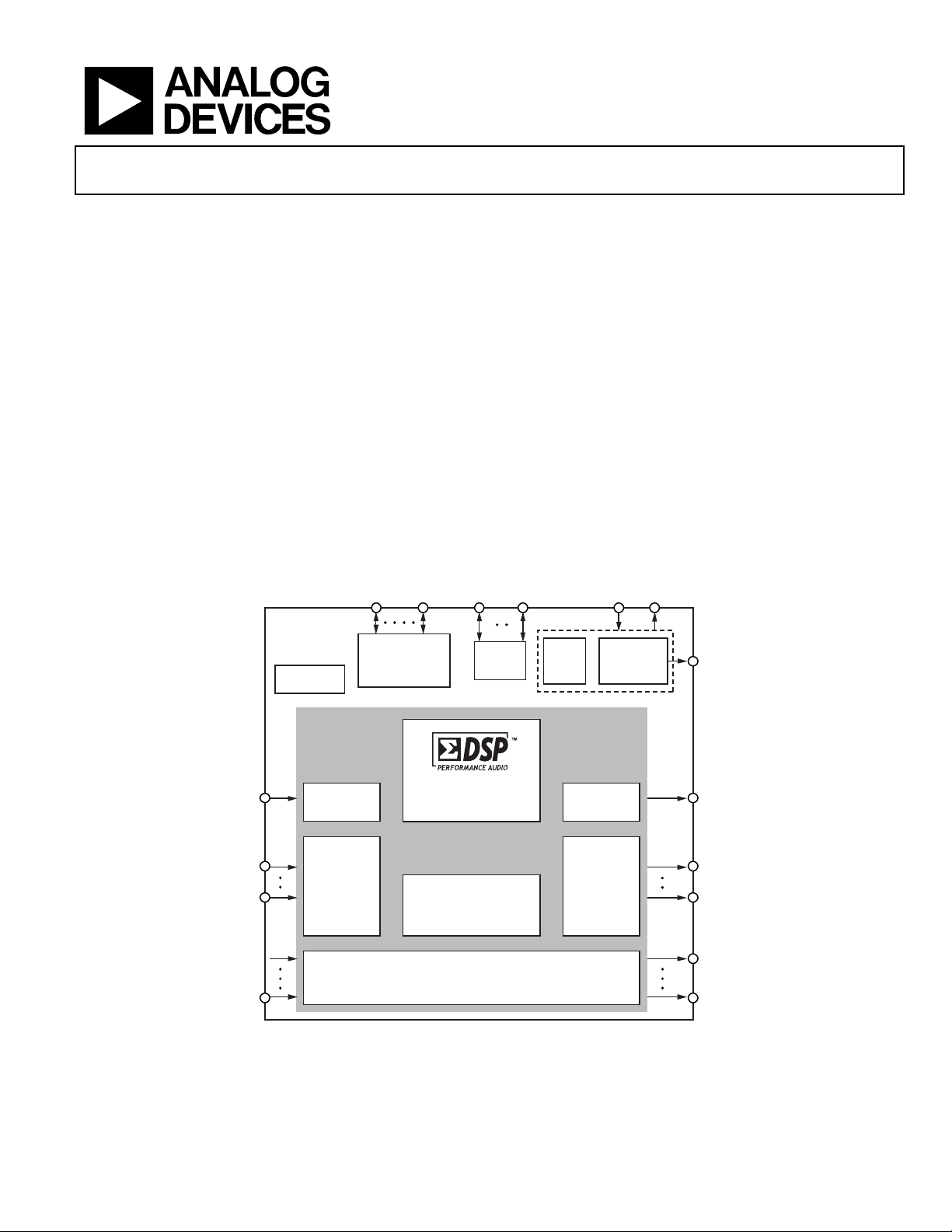
FUNCTIONAL BLOCK DIAGRAM
2
C* SELFBOOT
SPI/I
with Flexible Audio Routing Matrix
ADAU1445/ADAU1446
2
I
C and SPI control interfaces
Standalone operation
Self-boot from serial EEPROM
4-channel, 10-bit auxiliary control ADC
Multipurpose pins for digital controls and outputs
Easy implementation of available third-party algorithms
On-chip regulator for generating 1.8 V from 3.3 V supply
100-lead TQFP and LQFP packages
Temperature range: −40°C to +105°C
APPLICATIONS
Automotive audio processing
Head units
Navigation systems
Rear-seat entertainment systems
DSP amplifiers (sound system amplifiers)
Commercial audio processing
MP[3:0]/
MP[11:4]
ADC[3:0]
XTALI XTALO
ADAU1445/
ADAU1446
1.8V
REGULATOR
SPDIFI
SDATA_IN[8:0]
(24-CHANNEL
DIGITAL AUDI O
INPUT)
BIT CLOCK
FRAME CLOCK
*SPI/I
†
THERE ARE 12 BIT CLOCKS (BCLK[11:0]) AND 12 FRAM E CLOCKS (LRCL K[11:0]) IN T OTAL. OF THE 12 CL OCKS,
SIX ARE ASSI GNABLE, THREE MUST BE OUTPUTS, AND THREE M UST BE INPUTS.
†
(BCLK)
†
(LRCLK)
2
C = THE ADDR0, CLAT CH, S CL/CCLK, SDA/ COUT, AND ADDR1/CDATA P INS.
SERIAL DATA
INPUT PORT
S/PDIF
RECEIVER
(×9)
I2C/SPI CONT ROL
INTERFACE
AND SELF-BOO T
PROGRAMMABLE AUDIO
PROCESSOR CO RE
FLEXIBLE AUDIO ROUTING MATRIX
UP TO 16 CHANNELS OF
AUX ADC
(FARM)
ASYNCHRONOUS
SAMPLE RATE
CONVERTERS
SERIAL CLOCK
DOMAINS
(×12)
MP/
PLL
S/PDIF
TRANSMITTER
SERIAL DATA
OUTPUT PORT
(×9)
CLOCK
OSCILLATOR
CLKOUT
SPDIFO
SDATA_OUT[8:0]
(24-CHANNEL
DIGITAL AUDIO
OUTPUT)
BIT CLOCK
(BCLK)
FRAME CLOCK
(LRCLK)
†
†
07696-001
Figure 1.
Rev. A
Information furnished by Analog Devices is believed to be accurate and reliable. However, no
responsibility is assumed by Analog Devices for its use, nor for any infringements of patents or other
rights of third parties that may result from its use. Specifications subject to change without notice. No
license is granted by implication or otherwise under any patent or patent rights of Analog Devices.
Trademarks and registered trademarks are the property of their respective owners.
One Technology Way, P.O. Box 9106, Norwood, MA 02062-9106, U.S.A.
Tel: 781.329.4700 www.analog.com
Fax: 781.461.3113 ©2009 Analog Devices, Inc. All rights reserved.

ADAU1445/ADAU1446
TABLE OF CONTENTS
Features .............................................................................................. 1
Applications ....................................................................................... 1
Functional Block Diagram .............................................................. 1
Revision History ............................................................................... 2
General Description ......................................................................... 3
Specifications ..................................................................................... 4
Digital Timing Specifications ..................................................... 6
Absolute Maximum Ratings ............................................................ 9
Thermal Resistance ...................................................................... 9
ESD Caution .................................................................................. 9
Pin Configuration and Function Descriptions ........................... 10
Theory of Operation ...................................................................... 15
System Block Diagram ............................................................... 15
Overview ...................................................................................... 16
Initialization ................................................................................ 18
Master Clock and PLL ............................................................... 19
Voltage Regulator ....................................................................... 23
SRC Group Delay ....................................................................... 23
Control Port ................................................................................ 24
Serial Data Input/Output........................................................... 29
Serial Input Ports ........................................................................ 35
Serial Input Port Modes and Settings ...................................... 37
Serial Output Ports ..................................................................... 39
Serial Output Port Modes and Settings ................................... 40
Flexible Audio Routing Matrix (FARM) ................................. 44
Flexible Audio Routing Matrix Modes and Settings.............. 50
Asynchronous Sample Rate Converters .................................. 56
ASRC Modes and Settings ........................................................ 56
DSP Core ..................................................................................... 58
DSP Core Modes and Settings .................................................. 59
Reliability Features ..................................................................... 60
RAMs ........................................................................................... 62
S/PDIF Receiver and Transmitter ............................................ 63
S/PDIF Modes and Settings ...................................................... 64
Multipurpose Pins ...................................................................... 67
Multipurpose Pins Modes and Settings................................... 67
Auxiliary ADC ............................................................................ 68
Auxiliary ADC Modes and Settings ........................................ 68
Interfacing with Other Devices .................................................... 69
Drive Strength Modes and Settings ......................................... 69
Flexible TDM Modes ..................................................................... 74
Serial Input Flexible TDM Interface Modes and Settings..... 74
Serial Output Flexible TDM Interface Modes and Settings ........ 76
Software Features ............................................................................ 79
Software Safeload ....................................................................... 79
Software Slew .............................................................................. 79
Global RAM and Register Map .................................................... 80
Overview of Register Address Map ......................................... 80
Details of Register Address Map .............................................. 80
Applications Information .............................................................. 85
Layout Recommendations ........................................................ 85
Typical Application Schematics ................................................ 87
Outline Dimensions ....................................................................... 90
Ordering Guide .......................................................................... 90
REVISION HISTORY
4/09—Rev. 0 to Rev. A
Added ADAU1446 ............................................................. Universal
Added LQFP ........................................................................ Universal
Added Minimum Digital Current (DVDD) of ADAU1446,
Maximum Digital Current (DVDD) of ADAU1446, and
AVDD, DVDD, PVDD During Operation of ADAU1446
Parameters, Table 1 ....................................................................... 5
Changes to Table 4 ............................................................................ 9
Changes to Overview Section ....................................................... 16
Change to Table 9 ........................................................................... 21
Changes to Voltage Regulator Section ......................................... 23
Changes to EEPROM Format Section ......................................... 28
Changes to Serial Clock Domains Section .................................. 32
Rev. A | Page 2 of 92
Changes to Flexible Audio Routing Matrix—Input Side Section;
Added Figure 40; Renumbered Sequentially .......................... 46
Changes to Stereo ASRC Routing Overview Section ................ 47
Changes to ASRC Input Select Pairs[7:0] Registers (Address 0xE080
to Address 0xE087) Section ...................................................... 51
Changes to ASRC Output Rate Bits (Bits[5:0]) Section ............ 53
Changes to Serial Output Data Selector Bits
(Bits[5:0]) Section ....................................................................... 55
Changes to ASRC Modes and Settings Section .......................... 56
Added Table 43; Renumbered Sequentially ................................ 61
Updated Outline Dimensions ....................................................... 90
Changes to Ordering Guide .......................................................... 90
1/09—Revision 0: Initial Version

ADAU1445/ADAU1446
GENERAL DESCRIPTION
The ADAU1445/ADAU1446 are enhanced audio processors that
allow full flexibility in routing all input and output signals. The
SigmaDSP® core features full 28-bit processing (56-bit in doubleprecision mode), synchronous parameter loading for ensuring
filter stability, and 100% code efficiency with the SigmaStudio™
tools. This DSP allows system designers to compensate for the
real-world limitations of speakers, amplifiers, and listening
environments, resulting in a dramatic improvement of the
perceived audio quality through speaker equalization, multiband compression, limiting, and third-party branded algorithms.
The flexible audio routing matrix (FARM) allows the user to
multiplex inputs from multiple sources running at various
sample rates to or from the SigmaDSP core. This drastically
reduces the complexity of signal routing and clocking issues in
the audio system. FARM includes up to eight stereo asynchronous
sample rate converters (depending on the device model), Sony/
Philips Digital Interconnect Format (S/PDIF) input and output,
and serial (I
these inputs can be routed to the SigmaDSP core or to any of the
asynchronous sample rate converters (ASRCs). Similarly, any one
of the output signals can be taken from the SigmaDSP core or
2
S) and time division multiplexing (TDM) I/Os. Any of
from any of the ASRC outputs. This routing scheme, which can
be modified at any time via control registers, allows for maximum
system flexibility.
The ADAU1445 and ADAU1446 differ only in ASRC functionality
and packaging. The ADAU1445 contains 16 channels of ASRCs
and is packaged in a TQFP, whereas the ADAU1446 contains no
ASRCs and is packaged in an LQFP.
The ADAU1445/ADAU1446 can be controlled in one of two
operational modes. First, the settings of the chip can be loaded
and dynamically updated through the SPI/I
DSP can self-boot from an external EEPROM in a system with
no microcontroller. There is also a bank of multipurpose (MP) pins
that can be used as general-purpose digital I/Os or as inputs to
the 4-channel auxiliary control ADC.
The ADAU1445/ADAU1446 are supported by the SigmaStudio
graphical development environment. This software includes
audio processing blocks such as FIR and IIR filters, dynamics
processors, mixers, low level DSP functions, and third-party
algorithms for fast development of custom signal flows.
2
C® port. Second, the
Rev. A | Page 3 of 92

ADAU1445/ADAU1446
SPECIFICATIONS
AVDD = 3.3 V, DVDD = 1.8 V, PVDD = 3.3 V, IOVDD = 3.3 V, TA = 25°C, master clock input = 12.288 MHz, core clock f
unless otherwise noted.
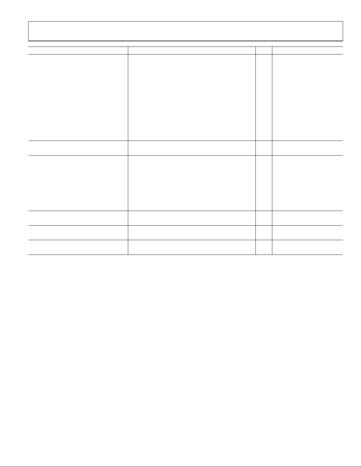
Table 1.
Parameter Min Typ Max Unit Test Conditions/Comments
ANALOG PERFORMANCE
Auxiliary Analog Inputs
Resolution 10 Bits
Full-Scale Analog Input AVDD V
Integral Nonlinearity (INL) −2.3 +2.3 LSB
Differential Nonlinearity (DNL) −2.0 +2.0 LSB
Gain Error −2.0 +2.0 LSB
Input Impedance 200 kΩ
Sample Rate f
/896 kHz
CORE
4:1 multiplexed input, each
channel at f
f
CORE
channel is sampled at 48 kHz.
DIGITAL I/O
Input Voltage, High (VIH) 0.7 × IOVDD V
Digital input pins except
SPDIFI.
Input Voltage, Low (VIL) 0.3 × IOVDD V
Digital input pins except
SPDIFI.
Input Leakage, High (IIH) at 3.3 V −2 +2 μA
Digital input pins except
MCLK and SPDIFI.
−2 +8 μA MCLK.
60 140 μA SPDIFI.
Input Leakage, Low (IIL) at 0 V −85 −10 μA All other pins.
−2 +2 μA
CLKMODEx, RSVD, PLLx,
RESET.
−8 +2 μA MCLK.
−140 −60 μA SPDIFI.
High Level Output Voltage (VOH) 0.85 × IOVDD V IOH = 1 mA.
Low Level Output Voltage (VOL) 0.1 × IOVDD V IOL = 1 mA.
Input Capacitance (Ci) 5 pF Guaranteed by design.
Multipurpose Pins Output Drive 2 6 mA
These pins are not designed
for static current draw and
should not drive LEDs directly.
2
POWER
Supply Voltage
Analog Voltage (AVDD) 2.97 3.3 3.63 V
Digital Voltage (DVDD) 1.62 1.8 1.98 V
PLL Voltage (PVDD) 2.97 3.3 3.63 V
IOVDD Voltage (IOVDD) 2.97 3.3 3.63 V
Supply Current
Analog Current (AVDD) 2 mA
PLL Current (PVDD) 10 mA
I/O Current (IOVDD) 10 mA
Depends greatly on the number of active serial ports, clock
pins, and characteristics of
external loads.
Minimum Digital Current (DVDD) of
ADAU1445
100 mA
Minimal program loaded,
one serial port active, no
ASRCs active.
= 172.032 MHz,
CORE
/3584. For
CORE
= 172.032 MHz, each
1
1
Rev. A | Page 4 of 92
ADAU1445/ADAU1446
Parameter Min Typ Max Unit Test Conditions/Comments
Maximum Digital Current (DVDD) of
ADAU1445
Minimum Digital Current (DVDD) of
ADAU1446
Maximum Digital Current (DVDD) of
ADAU1446
Power Dissipation
AVDD, DVDD, PVDD During Operation
of ADAU1445
AVDD, DVDD, PVDD During Operation
of ADAU1446
Reset, All Supplies 94 mW
TEMPERATURE RANGE
Functionality Guaranteed −40 +105 °C Ambient.
ASYNCHRONOUS SAMPLE RATE
CONVERTERS
Dynamic Range 139 dB A-weighted, 20 Hz to 20 kHz.
I/O Sample Rate 6 192 kHz
I/O Sample Rate Ratio 1:8 7.75:1
THD + N 120 133 −dB
Group Delay
CRYSTAL OSCILLATOR
Transconductance 40 mS
PLL
Lock Time 10 ms
REGULATOR
3
DVDD Voltage 1.65 1.75 1.85 V Maximum 500 mA load.
1
SPDIFI input voltage range exceeds the requirements of the S/PDIF specification.
2
Maximum specifications are measured across −40°C to +105°C ambient.
3
Regulator specifications are calculated using an NJT4030P transistor from On Semiconductor in the circuit.
260 310 mA
Full program loaded,
all serial ports active, all
ASRCs active.
100 mA
Minimal program loaded,
one serial port active.
195 235 mA
Full program loaded, all
serial ports active.
640 mW
IOVDD is not included in
measurement.
500 mW
IOVDD is not included in
measurement.
Refer to the SRC Group Delay
section.
Rev. A | Page 5 of 92

ADAU1445/ADAU1446
DIGITAL TIMING SPECIFICATIONS
TA = −40°C to +105°C, DVDD = 1.8 V, IOVDD = 3.3 V.
Table 2.
Parameter
MASTER CLOCK
f
tMP 40.69 354.36 ns
tMD 25 75 % Master clock (MCLK) duty cycle.
CLKOUT Jitter 250 ps Cycle-to-cycle rms average.
CORE CLOCK
f
SERIAL PORT
f
t
t
t
t
t
t
t
tTS 5 ns BCLKx output falling edge to LRCLKx output timing skew.
t
t
SPI PORT
f
f
t
t
t
t
t
t
t
t
t
I2C PORT
f
t
t
t
t
tDS 100 ns Data setup time.
tDH 0.9 μs Data hold time.
t
t
t
t
t
MULTIPURPOSE PINS AND RESET
fMP f
t
t
1
All timing specifications are given for the default (I2S) states of the serial audio input ports and the serial audio output ports (see Table 24 and Table 28).
2
Maximum SPI CCLK clock frequency is dependent on current drive strength and capacitive loads on the circuit board.
1
MP
172.032 MHz DSP core clock frequency.
CORE
24.576 MHz BCLK frequency.
BCLK
40.69 ns BCLK period.
BCLK
30 ns BCLKx low pulse width, slave mode.
BIL
30 ns BCLKx high pulse width, slave mode.
BIH
20 ns LRCLKx setup to BCLKx input rising edge, slave mode.
LIS
20 ns LRCLKx hold from BCLKx input rising edge, slave mode.
LIH
10 ns SDATA_INx setup to BCLKx input rising edge.
SIS
10 ns SDATA_INx hold from BCLKx input rising edge.
SIH
30 ns SDATA_OUTx delay in slave mode from BCLKx output falling edge.
SODS
30 ns SDATA_OUTx delay in master mode from BCLKx output falling edge.
SODM
32 MHz CCLK frequency.
CCLK write
16 MHz CCLK frequency.
CCLK read
20 ns CCLK pulse width low.
CCPL
20 ns CCLK pulse width high.
CCPH
0 ns CLATCH setup to CCLK rising edge.
CLS
35 ns CLATCH hold from CCLK rising edge.
CLH
20 ns CLATCH pulse width high.
CLPH
20 ns Minimum delay between CLATCH low pulses.
CLDLY
0 ns CDATA setup to CCLK rising edge.
CDS
35 ns CDATA hold from CCLK rising edge.
CDH
40 ns COUT valid output delay from CCLK falling edge.
COV
400 kHz SCL clock frequency.
SCL
0.6 μs SCL pulse width high.
SCLH
1.3 μs SCL pulse width low.
SCLL
0.6 μs Start and repeated start condition setup time.
SCS
0.6 μs Start condition hold time.
SCH
300 ns SCL rise time.
SCLR
300 ns SCL fall time.
SCLF
300 ns SDA rise time.
SDR
300 ns SDA fall time.
SDF
1.3 μs Bus-free time between stop and start.
BFT
1.5 × 1/f
MPIL
Min Max Unit Description
2.822 24.576 MHz
Master clock (MCLK) frequency. See the Master Clock and PLL section.
Master clock (MCLK) period. See the
/2 Hz MPx maximum switching rate.
S
μs MPx pin input latency until high/low value is read by core. Guaranteed by
S,NORMAL
Master Clock and PLL section.
2
2
design.
10 ns
RLPW
RESET
low pulse width.
Rev. A | Page 6 of 92
ADAU1445/ADAU1446
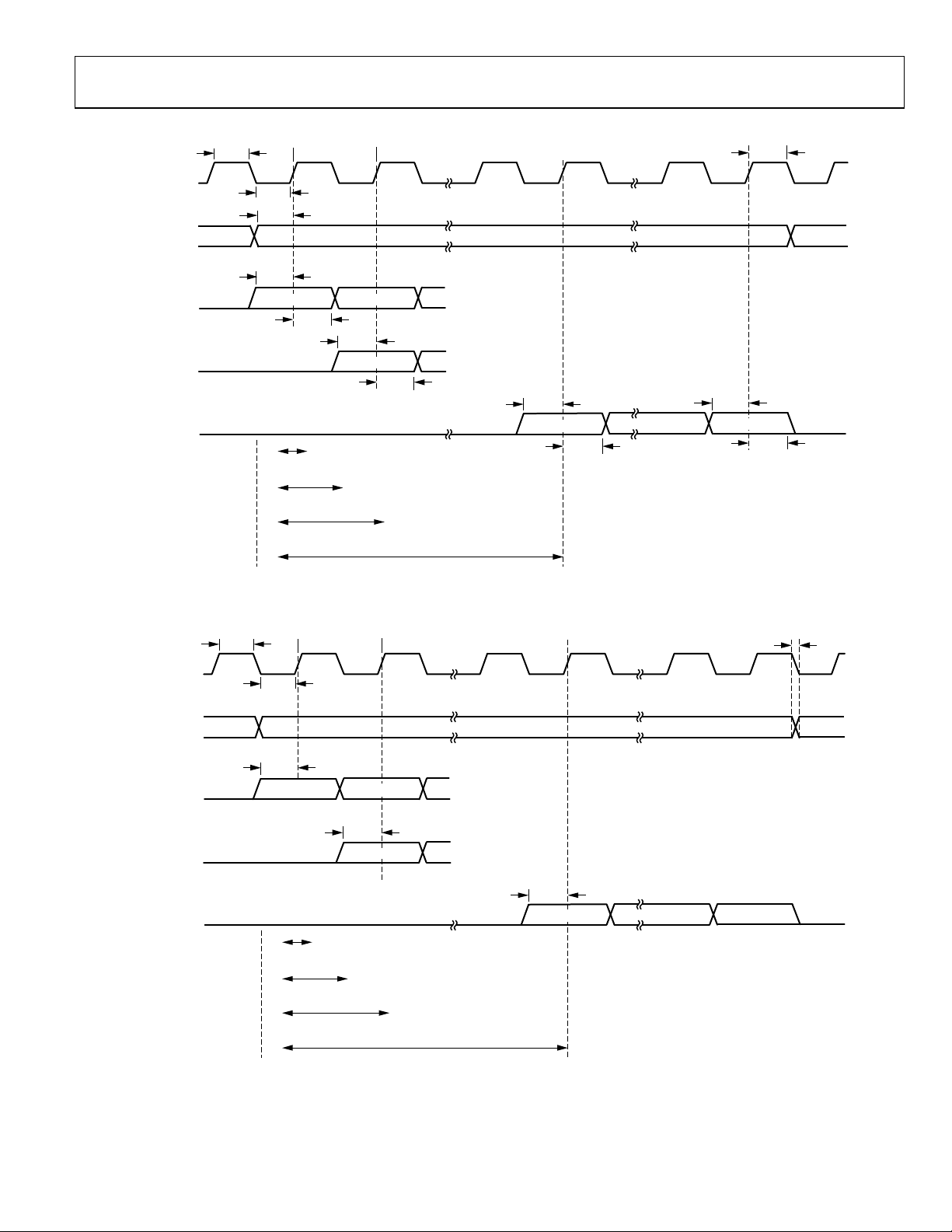
Digital Timing Diagrams
t
LIH
t
SIS
LSB
t
SIH
07696-002
t
TS
RIGHT-JUSTIFIED
BCLKx
INPUT
LRCLKx
INPUT
SDATA_INx
LEFT-JUSTIFIED
MODE
SDATA_INx
2
I
S MODE
SDATA_INx
MODE
BCLKx
OUTPUT
t
BIH
t
BIL
t
LIS
t
SIS
MSB
t
SIH
8-BIT CLOCKS
(24-BIT DATA)
12-BIT CLO CKS
(20-BIT DATA)
14-BIT CLO CKS
(18-BIT DATA)
16-BIT CLO CKS
(16-BIT DATA)
MSB – 1
t
SIS
MSB
t
SIH
t
SIS
MSB
t
SIH
Figure 2. Serial Input Port Timing
t
BIH
t
BIL
LRCLKx
OUTPUT
SDATA_OUTx
LEFT-JUSTIFIED
MODE
SDATA_OUTx
2
I
S MODE
SDATA_OUTx
RIGHT-JUSTIFIED
MODE
t
SODS
t
SODM
MSB
8-BIT CLO CKS
(24-BIT DAT A)
12-BIT CLOCKS
(20-BIT DAT A)
14-BIT CLOCKS
(18-BIT DAT A)
16-BIT CLOCKS
(16-BIT DAT A)
t
SODS
t
SODM
MSB – 1
MSB
Figure 3. Serial Output Port Timing
Rev. A | Page 7 of 92
t
SODS
t
SODM
MSB
LSB
07696-003
ADAU1445/ADAU1446
CLATCH
CCLK
CDATA
COUT
t
CLS
t
CCPL
t
CDS
t
CCPH
t
CDH
t
CLH
t
COV
t
CLPH
07696-004
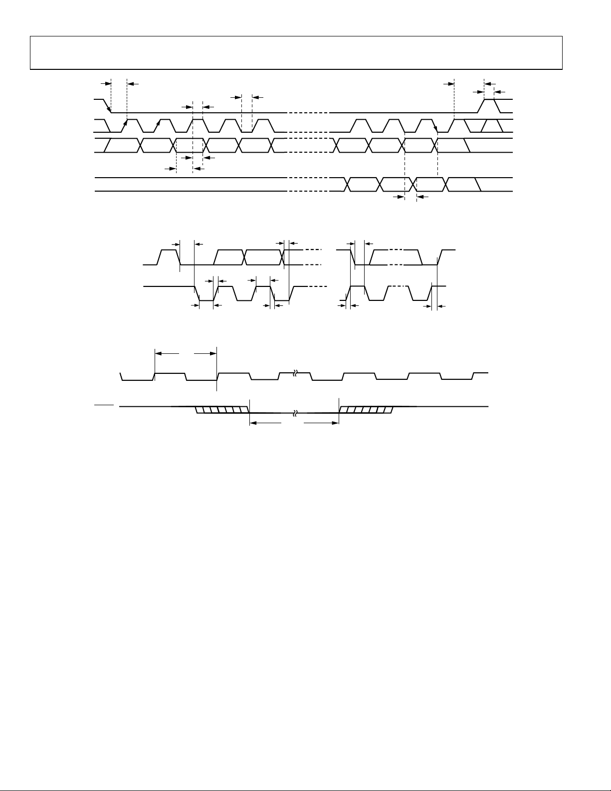
Figure 4. SPI Port Timing
t
DS
t
SCLH
Figure 5. I
t
2
C Port Timing
SCS
t
SCH
t
BFT
07696-005
SDA
SCL
t
SCH
t
SCLR
t
SCLLtSCLF
t
MP
MCLK
RESET
t
RLPW
07696-006
Figure 6. Master Clock and Reset Timing
Rev. A | Page 8 of 92
ADAU1445/ADAU1446
ABSOLUTE MAXIMUM RATINGS
Table 3.
Parameter Rating
DVDD to Ground 0 V to 2.2 V
AVDD to Ground 0 V to 4.0 V
IOVDD to Ground 0 V to 4.0 V
Digital Inputs DGND – 0.3 V to IOVDD + 0.3 V
Maximum Junction Temperature 150°C
Storage Temperature Range −65°C to +150°C
Soldering (10 sec) 300°C
Stresses above those listed under Absolute Maximum Ratings
may cause permanent damage to the device. This is a stress
rating only; functional operation of the device at these or any
other conditions above those indicated in the operational
section of this specification is not implied. Exposure to absolute
maximum rating conditions for extended periods may affect
device reliability.
THERMAL RESISTANCE
θJA is specified for the worst-case conditions, that is, a device
soldered in a circuit board for surface-mount packages.
Table 4. Thermal Resistance
Package Type θJA θ
100-Lead TQFP 26.3 9.4 °C/W
100-Lead LQFP 41.4 9.5 °C/W
Unit
JC
ESD CAUTION
Rev. A | Page 9 of 92
ADAU1445/ADAU1446
PIN CONFIGURATION AND FUNCTION DESCRIPTIONS
DVDD
SDATA_IN3
SDATA_OUT0
LRCLK4
BCLK4
SDATA_IN4
SDATA_OUT1
LRCLK5
BCLK5
SDATA_IN5
SDATA_OUT2
IOVDD
DGND
DVDD
LRCLK6
BCLK6
SDATA_IN6
SDATA_OUT3
LRCLK7
BCLK7
SDATA_IN7
SDATA_OUT4
LRCLK8
IOVDD
DGND
767778798081828384858687888990919293949596979899100
DVDD
DGND
IOVDD
BCLK3
LRCLK3
SDATA_IN2
BCLK2
LRCLK2
SDATA_IN1
BCLK1
LRCLK1
SDATA_IN0
BCLK0
DGND
IOVDD
LRCLK0
MP11
MP10
MP9
MP8
ADDR0
CLATCH
SCL/CCLK
SDA/COUT
ADDR1/CDATA
DVDD
1
PIN 1
2
3
4
5
6
7
8
9
10
11
12
13
14
15
16
17
18
19
20
21
22
23
24
25
26 27 28
29 30 31
ADAU1445/ADAU1446
TOP VIEW
(Not to S cale)
32
33 34 353637 38 39
41 42 43 44 45 46 47 48 49 50
40
75
BCLK8
74
SDATA_IN8
73
SDATA_OUT5
72
LRCLK9
71
BCLK9
70
SDATA_OUT6
69
LRCLK10
68
BCLK10
67
SDATA_OUT7
66
LRCLK11
65
BCLK11
64
IOVDD
63
DGND
62
SDATA_OUT8
61
PLL0
60
PLL1
59
MP0/ADC0
58
MP1/ADC1
57
56
MP2/ADC2
55
MP3/ADC3
54
RESET
53
CLKOUT
52
IOVDD
51
DGND
MP7
MP6
MP5
PLL2
DGND
IOVDD
SELFBOOT
NOTES
1. THE EXPOSED PAD DOES NOT HAVE AN INTERNAL EL E CTRICAL CONNECTI ON TO THE INTEGRATED CIRCUIT,
BUT SHOULD BE CONNECTED TO THE GROUND PLANE OF THE PCB FOR PROPER HEAT DISSIPATION.
RSVD
CLKMODE1
CLKMODE0
MP4
DVDD
DGND
IOVDD
XTALO
VDRIVE
PVDD
XTALI
PGND
PLL_FILT
AVDD
DVDD
SPDIFI
AGND
SPDIFO
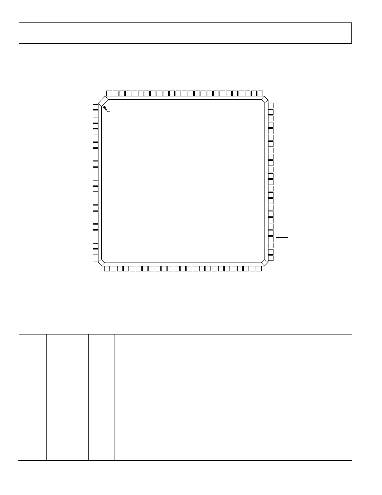
Figure 7. Pin Configuration
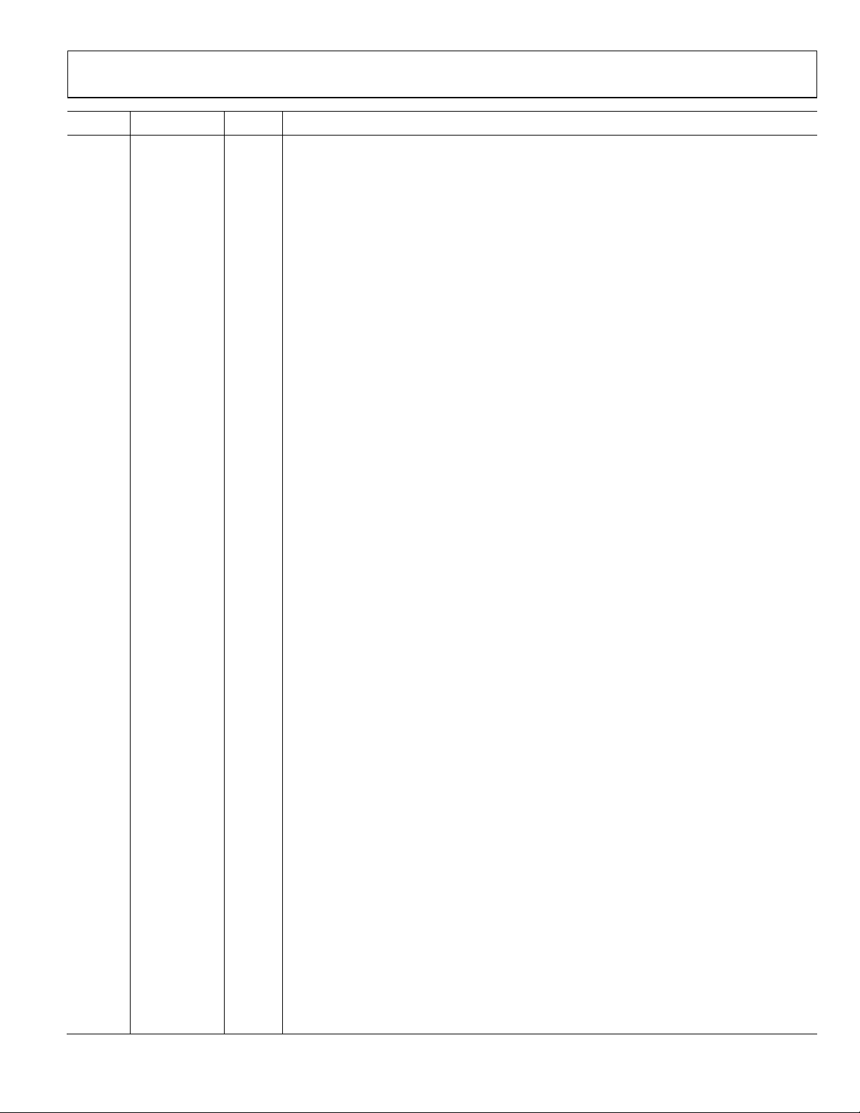
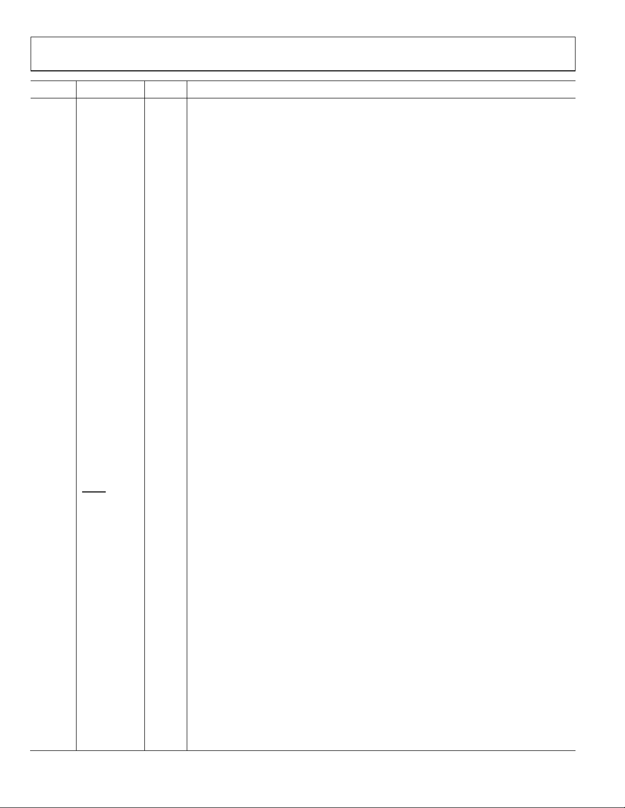
Table 5. Pin Function Descriptions
Pin No. Mnemonic Typ e
1, 13, 26,
DGND PWR
38, 51,
1
Description
Digital Ground. The AGND, DGND, and PGND pins should be tied directly together in a common
ground plane. DGND pins should be decoupled to a DVDD pin with a 100 nF capacitor.
62, 76,
88
2, 14, 27,
39, 52,
63, 77,
89
3 BCLK3 D_IO
IOVDD PWR
Input and Output Supply. The voltage on this pin sets the highest input voltage that should be
present on the digital input pins. This pin is also the supply for the digital output signals on the
clock, data, control port, and MP pins. IOVDD should always be set to 3.3 V. The current draw of this
pin is variable because it is dependent on the loads of the digital outputs.
Bit Clock, Input/Output Clock Domain 3. This pin is bidirectional, with the direction depending on
whether the Input/Output Clock Domain 3 is set up as a master or slave. When not used, this pin
can be left disconnected.
4 LRCLK3 D_IO
Frame Clock, Input/Output Clock Domain 3. This pin is bidirectional, with the direction depending on
whether the Input/Output Clock Domain 3 is set up as a master or slave. When not used, this pin
can be left disconnected.
5 SDATA_IN2 D_IN Serial Data Port 2 Input. When not used, this pin can be left disconnected.
07696-007
Rev. A | Page 10 of 92
ADAU1445/ADAU1446
Pin No. Mnemonic Typ e
6 BCLK2 D_IO
7 LRCLK2 D_IO
8 SDATA_IN1 D_IN Serial Data Port 1 Input. When not used, this pin can be left disconnected.
9 BCLK1 D_IO
10 LRCLK1 D_IO
11 SDATA_IN0 D_IN Serial Data Port 0 Input. When not used, this pin can be left disconnected.
12 BCLK0 D_IO
15 LRCLK0 D_IO
16 MP11 D_IO Multipurpose, General-Purpose Input/Output. When not used, this pin can be left disconnected.
17 MP10 D_IO Multipurpose, General-Purpose Input/Output. When not used, this pin can be left disconnected.
18 MP9 D_IO Multipurpose, General-Purpose Input/Output. When not used, this pin can be left disconnected.
19 MP8 D_IO Multipurpose, General-Purpose Input/Output. When not used, this pin can be left disconnected.
20 ADDR0 D_IN
21 CLATCH D_IN
22 SCL/CCLK D_IN
23 SDA/COUT D_IO
24 ADDR1/CDATA D_IN
25, 37,
DVDD PWR
50, 75,
87, 100
28 SELFBOOT D_IN
29 CLKMODE1 D_IN Output Clock Mode 1. With CLKMODE0, this pin sets the frequency of the CLKOUT signal.
30 CLKMODE0 D_IN Output Clock Mode 0. With CLKMODE1, this pin sets the frequency of the CLKOUT signal.
31 RSVD D_IN Reserved. Tie this pin to ground, preferably with a 10 kΩ pull-down resistor.
32 PLL2 D_IN PLL Mode Select Pin 2.
33 MP7 D_IO Multipurpose, General-Purpose Input/Output. When not used, this pin can be left disconnected.
1
Description
Bit Clock, Input Clock Domain 2. This pin is bidirectional, with the direction depending on whether
the Input Clock Domain 2 is set up as a master or slave. When not used, this pin can be left disconnected.
Frame Clock, Input Clock Domain 2. This pin is bidirectional, with the direction depending on whether
the Input Clock Domain 2 is set up as a master or slave. When not used, this pin can be left disconnected.
Bit Clock, Input Clock Domain 1. This pin is bidirectional, with the direction depending on whether
the Input Clock Domain 1 is set up as a master or slave. When not used, this pin can be left disconnected.
Frame Clock, Input Clock Domain 1. This pin is bidirectional, with the direction depending on whether
the Input Clock Domain 1 is set up as a master or slave. When not used, this pin can be left disconnected.
Bit Clock, Input Clock Domain 0. This pin is bidirectional, with the direction depending on whether
the Input Clock Domain 0 is set up as a master or slave. When not used, this pin can be left disconnected.
Frame Clock, Input Clock Domain 0. This pin is bidirectional, with the direction depending on whether
the Input Clock Domain 0 is set up as a master or slave. When not used, this pin can be left disconnected.
2
Address 0 for I
ADAU1445/ADAU1446 devices to be used on the same I
C and SPI. In I2C mode, this pin, in combination with ADDR1, allows up to four
2
C bus. In SPI mode, setting ADDR0 either
low or high allows up to two ICs to be used with a common SPI latch signal.
SPI Latch Signal. Must go low at the beginning of an SPI transaction and high at the end of a
transaction. Each SPI transaction may take a different number of CCLK cycles to complete,
depending on the address and read/write bits that are sent at the beginning of the SPI transaction.
When not used, this pin should be tied to ground, preferably with a 10 kΩ pull-down resistor.
2
Serial Clock/Continuous Clock. In I
input, except when in self-boot mode, where it is an open collector output (I
C mode, this pin functions as SCL and is always an open collector
2
C master). The line
connected to this pin should have a 2.0 kΩ pull-up resistor. In SPI mode, this pin functions as CCLK
and is an input pin that can either run continuously or be gated off between SPI transactions.
2
Serial Data/Continuous Output. In I
C mode, this pin functions as SDA and is a bidirectional open
collector. The line connected to the SDA pin should have a 2.0 kΩ pull-up resistor. In SPI mode, this
pin functions as COUT and is used for reading back registers and memory locations. The COUT pin
is three-stated when an SPI read is not active.
2
Address 1/Continuous Data. In I
ADDR0, sets the I
used on the same I
2
C address of the IC. This allows up to four ADAU1445/ADAU1446 devices to be
2
C bus. In SPI mode, this pin functions as CDATA and is the SPI data input.
C mode, this pin functions as ADDR1 and, in combination with
1.8 V Digital Supply. This can be supplied externally or generated from a 3.3 V supply with the on-board
1.8 V regulator. Each DVDD pin should be decoupled to DGND with a 100 nF capacitor.
Self-Boot Select. Allows the ADAU1445/ADAU1446 to be controlled by the control port or to
perform a self-boot. Setting this pin high (that is, to 1) initiates a self-boot operation when the
ADAU1445/ADAU1446 are brought out of a reset. This pin can be tied directly to a voltage source
or ground or pulled up/down with a resistor.
Rev. A | Page 11 of 92
ADAU1445/ADAU1446
D_IN
D_IO,
A_IN
D_IO,
A_IN
D_IO,
A_IN
D_IO,
A_IN
1
Description
Regulator Drive. Supplies the drive current for the 1.8 V regulator. The base of the voltage regulator’s
external PNP transistor is driven from VDRIVE.
Crystal Oscillator Output. A 100 Ω damping resistor should be connected between this pin and the
crystal. This output should not be used to directly drive a clock to another IC; the CLKOUT pin
exists for this purpose. If the crystal oscillator is not used, the XTALO pin can be left unconnected.
Crystal Oscillator Input. This pin provides the master clock for the ADAU1445/ADAU1446. If the
ADAU1445/ADAU1446 generate the master clock in the system, this pin should be connected to
the crystal oscillator circuit. If the ADAU1445/ADAU1446 are slaves to an external master clock, this
pin should be connected to the master clock signal generated by another IC.
Phase-Locked Loop Filter. Two capacitors and a resistor must be connected to this pin as shown in
Figure 11.
Phase-Locked Loop Supply. Provides the 3.3 V power supply for the PLL. This should be decoupled
to PGND with a100 nF capacitor.
Phase-Locked Loop Ground. Ground for the PLL supply. The AGND, DGND, and PGND pins can be
tied directly together in a common ground plane. PGND should be decoupled to PVDD with a
100 nF capacitor.
S/PDIF Input. Accepts digital audio data in the S/PDIF format. When not used, this pin can be left
disconnected.
S/PDIF Output. Outputs digital audio data in the S/PDIF format. When not used, this pin can be left
disconnected.
Analog Supply. 3.3 V analog supply for the auxiliary ADC. This pin should be decoupled to AGND
with a 100 nF capacitor.
Analog Ground. Ground for the analog supply. This pin should be decoupled to AVDD with a
100 nF capacitor.
Master Clock Output. Used to output a master clock to other ICs in the system. Set using the
CLKMODEx pins. When not used, this pin can be left disconnected.
Reset. Active-low reset input. Reset is triggered on a high-to-low edge and exited on a low-to-high
edge. For detailed information about initialization, see the Power-Up Sequence section. A reset
event sets all RAMs and registers to their default values.
Multipurpose, General-Purpose Input or Output/Auxiliary ADC Input 3. When not used, this pin can
be left disconnected.
Multipurpose, General-Purpose Input or Output/Auxiliary ADC Input 2. When not used, this pin can
be left disconnected.
Multipurpose, General-Purpose Input or Output/Auxiliary ADC Input 1. When not used, this pin can
be left disconnected.
Multipurpose, General-Purpose IO/Auxiliary ADC Input 0. When not used, this pin can be left
disconnected.
Bit Clock, Output Clock Domain 2. This pin is bidirectional, with the direction depending on whether the
Output Clock Domain 2 is set up as a master or slave. When not used, this pin can be left disconnected.
Frame Clock, Output Clock Domain 2. This pin is bidirectional, with the direction depending on
whether the Output Clock Domain 2 is set up as a master or slave. When not used, this pin can be
left disconnected.
Pin No. Mnemonic Typ e
34 MP6 D_IO Multipurpose, General-Purpose Input/Output. When not used, this pin can be left disconnected.
35 MP5 D_IO Multipurpose, General-Purpose Input/Output. When not used, this pin can be left disconnected.
36 MP4 D_IO Multipurpose, General-Purpose Input/Output. When not used, this pin can be left disconnected.
40 VDRIVE A_OUT
41 XTALO A_OUT
42 XTALI A_IN
43 PLL_FILT A_OUT
44 PVDD PWR
45 PGND PWR
46 SPDIFI D_IN
47 SPDIFO D_OUT
48 AVDD PWR
49 AGND PWR
53 CLKOUT D_OUT
54
RESET
55 MP3/ADC3
56 MP2/ADC2
57 MP1/ADC1
58 MP0/ADC0
59 PLL1 D_IN Phase-Locked Loop Mode Select Pin 1.
60 PLL0 D_IN Phase-Locked Loop Mode Select Pin 0.
61 SDATA_OUT8 D_OUT Serial Data Port 0 Output. When not used, this pin can be left disconnected.
64 BCLK11 D_IO
65 LRCLK11 D_IO
Rev. A | Page 12 of 92
ADAU1445/ADAU1446
Pin No. Mnemonic Typ e
66 SDATA_OUT7 D_OUT Serial Data Port 7 Output. When not used, this pin can be left disconnected.
67 BCLK10 D_IO
68 LRCLK10 D_IO
69 SDATA_OUT6 D_OUT Serial Data Port 6 Output. When not used, this pin can be left disconnected.
70 BCLK9 D_IO
71 LRCLK9 D_IO
72 SDATA_OUT5 D_OUT Serial Data Port 5 Output. When not used, this pin can be left disconnected.
73 SDATA_IN8 D_IN Serial Data Port 8 Input. When not used, this pin can be left disconnected.
74 BCLK8 D_IO
78 LRCLK8 D_IO
79 SDATA_OUT4 D_OUT Serial Data Port 4 Output. When not used, this pin can be left disconnected.
80 SDATA_IN7 D_IN Serial Data Port 7 Input. When not used, this pin can be left disconnected.
81 BCLK7 D_IO
82 LRCLK7 D_IO
83 SDATA_OUT3 D_OUT Serial Data Port 3 Output. When not used, this pin can be left disconnected.
84 SDATA_IN6 D_IN Serial Data Port 6 Input. When not used, this pin can be left disconnected.
85 BCLK6 D_IO
86 LRCLK6 D_IO
90 SDATA_OUT2 D_OUT Serial Data Port 2 Output. When not used, this pin can be left disconnected.
91 SDATA_IN5 D_IN Serial Data Port 5 Input. When not used, this pin can be left disconnected.
92 BCLK5 D_IO
93 LRCLK5 D_IO
94 SDATA_OUT1 D_OUT Serial Data Port 1 Output. When not used, this pin can be left disconnected.
95 SDATA_IN4 D_IN Serial Data Port 4 Input. When not used, this pin can be left disconnected.
1
Description
Bit Clock, Output Clock Domain 10. This pin is bidirectional, with the direction depending on whether
the Output Clock Domain 10 is set up as a master or slave. When not used, this pin can be left
disconnected.
Frame Clock, Output Clock Domain 10. This pin is bidirectional, with the direction depending on
whether the Output Clock Domain 10 is set up as a master or slave. When not used, this pin can be
left disconnected.
Bit Clock, Output Clock Domain 9. This pin is bidirectional, with the direction depending on whether the
Output Clock Domain 9 is set up as a master or slave. When not used, this pin can be left disconnected.
Frame Clock, Output Clock Domain 9. This pin is bidirectional, with the direction depending on
whether the Output Clock Domain 9 is set up as a master or slave. When not used, this pin can be
left disconnected.
Bit Clock, Input/Output Clock Domain 8. This pin is bidirectional, with the direction depending on
whether the Input/Output Clock Domain 8 is set up as a master or slave. When not used, this pin
can be left disconnected.
Frame Clock, Input/Output Clock Domain 8. This pin is bidirectional, with the direction depending
on whether the Input/Output Clock Domain 8 is set up as a master or slave. When not used, this
pin can be left disconnected.
Bit Clock, Input/Output Clock Domain 7. This pin is bidirectional, with the direction depending on
whether the Input/Output Clock Domain 7 is set up as a master or slave. When not used, this pin
can be left disconnected.
Frame Clock, Input/Output Clock Domain 7. This pin is bidirectional, with the direction depending
on whether the Input/Output Clock Domain 7 is set up as a master or slave. When not used, this
pin can be left disconnected.
Bit Clock, Input/Output Clock Domain 6. This pin is bidirectional, with the direction depending on
whether the Input/Output Clock Domain 6 is set up as a master or slave. When not used, this pin
can be left disconnected.
Frame Clock, Input/Output Clock Domain 6. This pin is bidirectional, with the direction depending
on whether the Input/Output Clock Domain 6 is set up as a master or slave. When not used, this
pin can be left disconnected.
Bit Clock, Input/Output Clock Domain 5. This pin is bidirectional, with the direction depending on
whether the Input/Output Clock Domain 5 is set up as a master or slave. When not used, this pin
can be left disconnected.
Frame Clock, Input/Output Clock Domain 5. This pin is bidirectional, with the direction depending
on whether the Input/Output Clock Domain 5 is set up as a master or slave. When not used, this
pin can be left disconnected.
Rev. A | Page 13 of 92
ADAU1445/ADAU1446
Pin No. Mnemonic Typ e
96 BCLK4 D_IO
97 LRCLK4 D_IO
98 SDATA_OUT0 D_OUT Serial Data Port 0 Output. When not used, this pin can be left disconnected.
99 SDATA_IN3 D_IN Serial Data Port 3 Output. When not used, this pin can be left disconnected.
1
PWR = power/ground, A_IN = analog input, D_IN = digital input, A_OUT = analog output, D_OUT = digital output, D_IO = digital input/output.
1
Description
Bit Clock, Input/Output Clock Domain 4. This pin is bidirectional, with the direction depending on
whether the Input/Output Clock Domain 4 is set up as a master or slave. When not used, this pin
can be left disconnected.
Frame Clock, Input/Output Clock Domain 4. This pin is bidirectional, with the direction depending
on whether the Input/Output Clock Domain 4 is set up as a master or slave. When not used, this
pin can be left disconnected.
Rev. A | Page 14 of 92
ADAU1445/ADAU1446
K
THEORY OF OPERATION
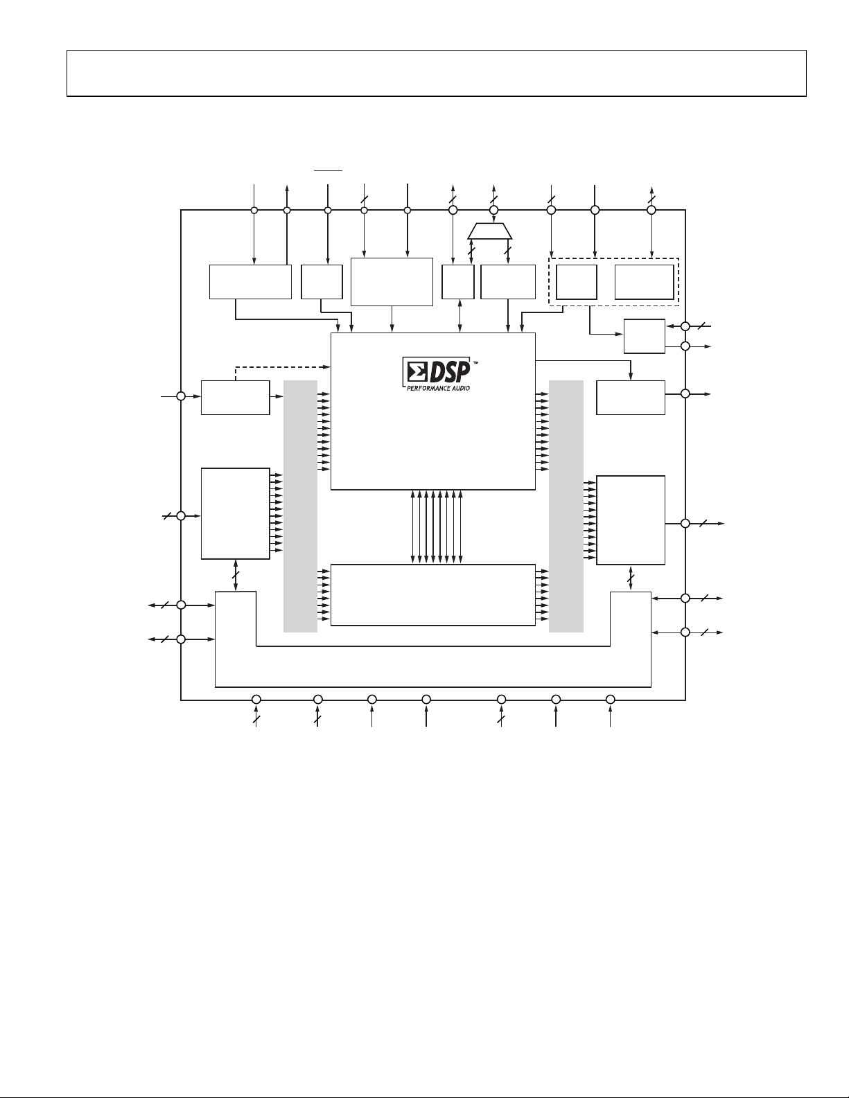
SYSTEM BLOCK DIAGRAM
MP[3:0]/
MP[11:4]SPI/I
ADC[3:0]
85
4
PLL[2:0] PLL_FILT
4
XTALI, XTAL ORESET
234
ADAU1445/
ADAU1446
+3.3V VDRIVE
2
C* SELFBOOT
SDATA_IN[8:0]
(24-CHANNEL
DIGITAL AUDIO
BIT CLOCK
(BCLK)
FRAME CLOC
(LRCLK)
SPDIFI
INPUT)
†
†
9
3TO 9
3TO 9
1.8V REGULATOR
S/PDIF
RECEIVER
SERIAL DATA
INPUT PORT
(×9)
9
FLEXIBLE AUDIO ROUT ING MATRIX
RESET
(INPUT SIDE )
I2C/SPI CONT ROL
INTERFACE
AND SELF-BO OT
28-/56-BIT, 172MHz
PROGRAMMABLE AUDIO
PROCESSOR CORE,
170ms DELAY MEMORY
UP TO 16 CHANNELS OF
ASYNCHRONOUS
SAMPLE RATE
CONVERTERS
SERIAL CLOCK
DOMAINS
(×12)
MP
AUXILIARY
ADC
PLL
(OUTPUT SIDE)
FLEXIBLE AUDIO ROUT ING MATRIX
CLOCK
OSCILLATOR
CLOCK
OUTPUT
S/PDIF
TRANSMITTER
SERIAL DATA
OUTPUT PORT
(×9)
9
2
9
3TO 9
3TO 9
CLKMODE[1:0]
CLKOUT
SPDIFO
SDATA_OUT[8:0]
(24-CHANNEL
DIGITAL AUDIO
OUTPUT)
BIT CLOCK
(BCLK)
FRAME CLOCK
(LRCLK)
†
†
DVDD DGND AVDD AGND
2
*SPI/I
C = THE ADDR0, CLAT CH, SCL/CCLK, SDA/COUT, AND ADDR1/CDATA PINS.
†
THERE ARE 12 BIT CLOCKS (BCL K[ 11: 0]) AND 12 FRAME CLOCKS (LRCLK[ 11: 0] ) IN TOTAL . OF T HE 1 2 CLOCKS,
SIX ARE ASSI GNABLE, THREE M US T BE OUTPUT S , AND THREE MUST BE INPUTS.
Figure 8. System Block Diagram
Rev. A | Page 15 of 92
IOVDD
886
PVDD PGND
07696-008

ADAU1445/ADAU1446
OVERVIEW
The ADAU1445/ADAU1446 are each a 24-channel audio DSP with
an integrated S/PDIF receiver and transmitter, flexible serial audio
ports, up to 16 channels of asynchronous sample rate converters
(ASRCs), flexible audio routing, and user interface capabilities.
Signal processing capabilities include equalization, crossover,
bass enhancement, multiband dynamics processing, delay compensation, speaker compensation, and stereo image widening.
These algorithms can be used to compensate for the real-world
limitations of speakers, amplifiers, and listening environments,
resulting in an improvement in perceived audio quality.
An on-board oscillator can be connected to an external crystal
to generate the master clock. A phase-locked loop (PLL) allows
the ADAU1445/ADAU1446 to be clocked from a variety of clock
frequencies. The PLL can accept inputs of 64 × f
384 × f
, or 512 × fS to generate the internal master clock of the core,
S
where f
is the sampling rate of audio in normal-rate processing
S
mode. In dual or quad rate mode, these multipliers are halved
or quartered, respectively. System sample rates include, but are
not limited to, 44.1 kHz, 48 kHz, 88.2 kHz, 96 kHz, and 192 kHz.
Each ADAU1445/ADAU1446 operates from a 1.8 V digital power
supply and a 3.3 V analog supply. An on-board voltage regulator
can be used to operate the chip from a single 3.3 V supply.
The ADAU1445/ADAU1446 have a sophisticated control port
that supports complete read and write capability of all memory
locations, excluding read-only addresses. Control registers are
provided to offer complete control of the chip’s configuration
and serial modes. Handshaking is included for ease of memory
uploads and downloads. The ADAU1445/ADAU1446 can be
configured for either SPI or I
2
C control. Program RAM, parameter
RAM, and register contents can be saved in an external EEPROM,
from which the ADAU1445/ADAU1446 can self-boot on startup.
The ADAU1445/ADAU1446 serial ports operate with digital audio
I/Os in the I
2
S, left-justified, right-justified, or TDM-compatible
mode. The flexible serial data ports allow for direct interconnection
to a variety of ADCs, DACs, and general-purpose DSPs. The
combination of an on-board S/PDIF transmitter and receiver
and 16 channels of ASRCs allows for easy compatibility with an
extensive number of external devices, and a system with up to
nine sampling rates.
The flexible audio routing matrix (FARM) is a system of multiplexers used to distribute the audio signals in the ADAU1445/
ADAU1446 among the serial inputs and outputs, audio core,
and ASRCs. FARM can easily be configured by setting the
appropriate registers.
The ADAU1445 and ADAU1446 are distinguished by the number
of on-board ASRCs and maximum sample rates. The ADAU1445
contains two 8-channel ASRCs, and the ADAU1446 has no ASRCs.
Two sets of serial ports at the input and output can operate in a
special flexible TDM mode, which allows the user to independently
, 128 × fS, 256 × fS,
S
assign byte-specific locations to audio streams at varying bit
depths. This mode ensures compatibility with codecs using
similar flexible TDM streams.
The core of the ADAU1445/ADAU1446 is a 28-bit DSP (or a
56-bit DSP when using double-precision mode) optimized for
audio processing, and it can process audio at sample rates of up
to 192 kHz. The program and parameter RAMs can be loaded with
a custom audio processing signal flow built with the SigmaStudio
graphical programming software from Analog Devices, Inc. The
values stored in the parameter RAM control individual signal processing blocks, such as IIR and FIR equalization filters, dynamics
processors, audio delays, and mixer levels. A software safeload
feature allows for transparent parameter updates and prevents
clicks on the output signals.
Reliability features such as a CRC and program counter watchdog
help ensure that the system can detect and recover from any
errors related to memory corruption.
S/PDIF signals can be routed through an ASRC for processing
in the DSP or can be sent directly to output on MP pins for
recovery of the embedded audio signal. Other components of
the embedded signal, including status and user bits, are not lost
and can be output on the MP pins as well.
Multipurpose (MP) pins are available for providing a simple
user interface without the need for an external microcontroller.
Twelve pins are available to input external control signals and
output flags or controls to other devices in the system. Four of
these can alternatively be assigned to an auxiliary ADC for use
with analog controls such as potentiometers or system voltages.
As inputs, MP pins can be connected to push buttons, switches,
rotary encoders, potentiometers, or other external control circuitry
to control the internal signal processing program. When configured as outputs, these pins can be used to drive LEDs (with a
buffer), to output flags to a microcontroller, to control other ICs,
or to connect to other external circuitry in an application.
The SigmaStudio software is used to program and control the
ADAU1445/ADAU1446 through the control port. Along with
designing and tuning a signal flow, the software can configure
all of the DSP registers in real time and download a new program
and parameter into the external self-boot EEPROM. SigmaStudio’s
easy-to-use graphical interface allows anyone with audio processing
knowledge to easily design a DSP signal flow and port it to a target
application without the need for writing line-level code. At the
same time, the software provides enough flexibility and programmability for an experienced DSP programmer to have in-depth
control of the design. In SigmaStudio, the user can add signal
processing cells from the library by dragging and dropping cells,
connect them together in a flow, compile the design, and load
the program and parameter files into the ADAU1445/ADAU1446
memory through the control port. The complicated tasks of
linking, compiling, and downloading the project are all handled
automatically by the software.
Rev. A | Page 16 of 92

ADAU1445/ADAU1446
Signal processing algorithms available in the provided libraries
include
• Single- and double-precision biquad filter
• Mono and multichannel dynamics processors with peak or
RMS detection
• Mixer and splitter
• Tone and noise generator
• Fixed and variable gain
• Loudness
• Delay
• Stereo enhancement
• Dynamic bass boost
• Noise and tone source
• Level detector
• MP pin control and conditioning
New processing algorithms are always being developed. Analog
Devices also provides proprietary and third-party algorithms
for applications such as matrix decoding, bass enhancement, and
surround virtualizers. Contact Analog Devices for information
about licensing these algorithms.
Several power-saving mechanisms have been designed into the
ADAU1445/ADAU1446, including programmable pad strength
for digital I/O pins and the ability to block the master clock
from reaching unused subsystems.
The ADAU1445/ADAU1446 are fabricated on a single monolithic integrated circuit for operation over the −40°C to +105°C
temperature range. The ADAU1445 is housed in a 100-lead
TQFP package, with an exposed pad to assist in heat dissipation,
and the ADAU1446, due to its lower power consumption, is
housed in a 100-lead LQFP package.
Rev. A | Page 17 of 92
ADAU1445/ADAU1446
INITIALIZATION
Power-Up Sequence
The ADAU1445/ADAU1446 have a built-in initialization period,
which allows sufficient time for the PLL to lock and the registers
to initialize their values. On a positive edge of
settings are immediately set by the PLL0, PLL1, and PLL2 pins,
and the master clock signal is blocked from the chip subsystems.
The initialization time lasts 10 ms, which is measured from the
rising edge of
control port until the initialization is complete.
Tabl e 6 shows some typical times to boot the ADAU1445/
ADAU1446 into the operational state necessary for an application,
assuming that a 400 kHz I
and a full program, parameter set, and all registers (9 kB) are
loaded. In reality, most applications use less than this full amount,
and unused program and parameter RAM need not be initialized;
therefore, the total boot time may be shorter.
. New values should not be written via the
RESET
2
C clock or a 5 MHz SPI clock is used
Recommended Program/Parameter Loading Procedure
When writing large amounts of data to the program or parameter
RAM in direct write mode, such as when downloading the initial
contents of the RAMs from an external memory, the processor core
should be disabled to prevent unpleasant noises from appearing
at the audio output. When small amounts of data are transmitted
during real-time operation of the DSP, such as when updating
individual parameters, the software safeload mechanism can be
used. More information is available in the Software Safeload section.
Power-Reduction Modes
Sections of the ADAU1445/ADAU1446 chips can be turned on
and off as needed to reduce power consumption. These include
the ASRCs, S/PDIF receiver and transmitter, auxiliary ADCs,
RESET
, the PLL
and DSP core. More information is available in the Master
Clock and PLL Modes and Settings section.
System Initialization Sequence
Before the IC can process audio in the DSP, the following initialization sequence must be completed. (Step 5 through Step 11
can be performed in any order, as needed.)
1. Power on the IC and bring it out of reset. The order of the
power supplies (DVDD, IOVDD, and AVDD) does not matter.
2. Wait at least 10 ms for the initialization to complete.
3. Enable the master clocks of all modules to be used (see the
Master Clock and PLL Modes and Settings section).
4. Deassert the core run bit (see the DSP Core Modes and
Settings section).
5. Set the serial input modes (see the Serial Input Port Modes
Registers (Address 0xE000 to Address 0xE008) section).
6. Set the serial output modes (see the Serial Output Port
Modes Registers (Address 0xE040 to Address 0xE049 section).
7. Set the routing matrix modes (see details of Address 0xE080
to Address 0xE09B in the Flexible Audio Routing Matrix
Modes section).
8. Set the DSP core rate select registers (see the DSP Core
Rate Select Register (Address 0xE220) section).
9. Write the parameter RAM (Address 0x0000 to Address
0x0FFF).
10. Write the program RAM (Address 0x2000 to Address
0x2FFF).
11. Write all other necessary control registers, such as ASRCs
and S/PDIF (Address 0xE221 to Address 0xE24C).
12. Assert the core run bit (see the DSP Core Modes and
Settings section).
Table 6. Power-Up Time
Approximate Boot Time; Loading Maximum Program/Parameter/Registers (ms)
PLL Lock Time (ms)
10 25 2 0.4 10.4 to 35
Rev. A | Page 18 of 92
Total (ms) I2C (@ 400 kHz SCL) SPI (@ 5 MHz CCLK) SPI (@ 25 MHz CCLK)
ADAU1445/ADAU1446
C
C
MASTER CLOCK AND PLL
Using the Oscillator
The ADAU1445/ADAU1446 can use an on-board oscillator to
generate its master clock. However, an external crystal must be
attached to complete the oscillator circuit. The on-board oscillator
is designed to work with a 256 × f
12.288 MHz when f
is 44.1 kHz. The resonant frequency of this crystal should
f
S,NORMAL
is 48 kHz and 11.2896 MHz when
S,NORMAL
be in this range even in the case when the core is processing
dual- or quad-rate signals. When the core is processing dualrate signals (for example, f
= 88.2 kHz or 96 kHz), resonant
S,DUAL
frequency of the crystal should be 128 × f
processing quad-rate signals (for example, f
the resonant frequency of the crystal should be 64 × f
The external crystal in the circuit should be an AT-cut parallel
resonance device operating at its fundamental frequency.
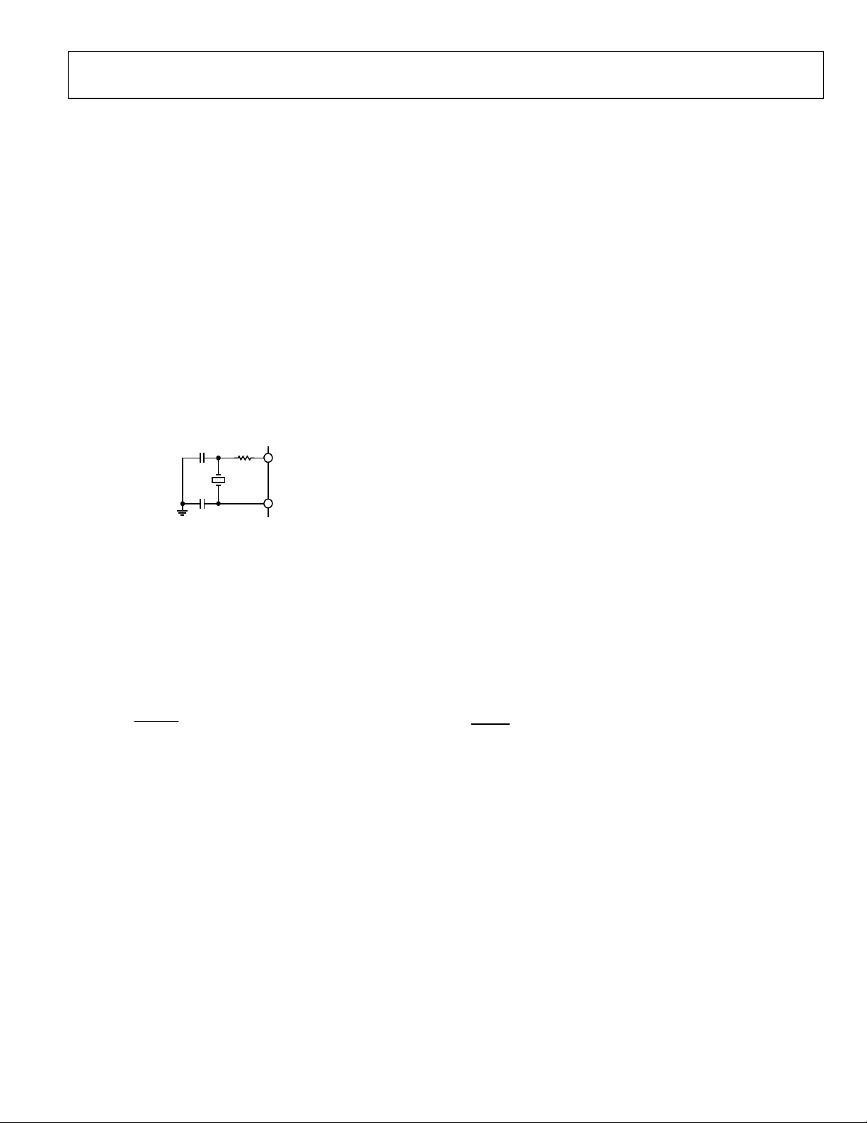
Ceramic resonators should not be used. Figure 9 shows the
crystal oscillator circuit recommended for proper operation.
C1
100Ω
C2
Figure 9. Crystal Oscillator Circuit
The 100 damping resistor on XTALO provides the oscillator
with a voltage swing of approximately 2.2 V at the XTALI pin.
The crystal shunt capacitance should be 7 pF. Its optimal load
capacitance, specified by the manufacturer, should be about 18 pF,
although the circuit supports values up to 25 pF. The equivalent
series resistance should also be as small as possible. The necessary
values of Load Capacitor C1 and Load Capacitor C2 can be
calculated from the crystal load capacitance with the following
equation:
×
C +
L
where C
STRAY
=
21
C
STRAY
CC
+
21
is the stray capacitance in the circuit and is usually
assumed to be approximately 2 pF to 5 pF.
Short trace lengths in the oscillator circuit decrease stray
capacitance, thereby increasing the loop gain of the circuit and
helping to avoid crystal start-up problems.
On the ADAU1445/ADAU1446 evaluation boards, the capacitance value for C1 and C2 is 22 pF.
XTALO should not be used to directly drive the crystal signal to
another IC. This signal is an analog sine wave and is not appropriate to drive a digital input. A separate pin, CLKOUT, is provided
master clock, which is
S,NORMAL
; when the core is
S,DUAL
S,QUAD
XTALO
XTALI
07696-009
= 192 kHz),
.
S,QUAD
for this purpose. CLKOUT can output 256 × f
f
, or a buffered, digital copy of the crystal oscillator
S,NORMAL
signal to other ICs in the system. CLKOUT is set up using the
CLKMODEx pins. For a more detailed explanation of CLKOUT,
refer to the Using the ADAU1445/ADAU1446 as Clock Master
section.
Setting Master Clock and PLL Mode
The ADAU1445/ADAU1446 master clock input feeds a PLL, which
generates the 3584 × f
clock (172.032 MHz when f
S,NORMAL
is 48 kHz) to run the DSP core. This rate is referred to as f
In normal operation, the input to the master clock must be one
of the following: 64 × f
384 × f
S,NORMAL
, or 512 × f
S,NORMAL
S,NORMAL
, 128 × f
, where f
S,NORMAL
S,NORMAL
sampling rate with the core in normal-rate processing mode.
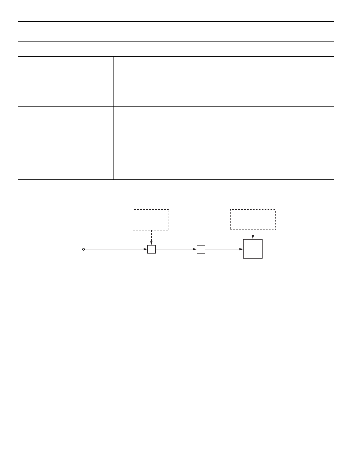
The PLL divider mode is set by PLL0, PLL1, and PLL2 as
detailed in Tab le 7 .
If the ADAU1445/ADAU1446 cores are set to receive dual-rate
signals (by reducing the number of program steps per sample by
a factor of 2 using the DSP core rate select register), then the master
clock frequency must be 32 × f
192 × f
S,DUAL
, or 256 × f
S,DUAL
.
S,DUAL
, 64 × f
S,DUAL
If the ADAU1445/ADAU1446 cores are set to receive quad-rate
signals (by reducing the number of program steps per sample by
a factor of 4 using the DSP core rate select register), then the master
clock frequency must be 16 × f
96 × f
S,QUAD
, or 128 × f
. On power-up, a clock signal must
S,QUAD
S,QUAD
, 32 × f
S,QUAD
be present on XTALI so that the ADAU1445/ADAU1446 can
complete its initialization routine.
If, at any point during operation, the clock signal is removed
from XTALI, the DSP should be reset to avoid unpredictable
behavior on output pins. The clock mode should not be changed
without also resetting the ADAU1445/ADAU1446. If the mode
is changed during operation, a click or pop can result on the
outputs. The state of the PLLx pins should be changed while
is held low.
RESET
The phase-locked loop uses the PLL mode select pins (PLL0,
PLL1, and PLL2) to derive a 64 × f
clock from whatever
S,NORMAL
signal is present at the XTALI pin. This clock signal is multiplied
by 56 to produce the core clock. Therefore, f
In a system with a f
of 48 kHz, the PLL derives a 3.072 MHz
S,NORMAL
CORE
clock and then multiplies it by 56 to produce a 172.032 MHz
core clock.
The core clock (f
) should never exceed 172.032 MHz,
CORE
though it may be lower in some applications.
, 512 ×
S,NORMAL
, 256 × f
is the audio
, 128 × f
, 64 × f
is 3584 × f
S,NORMAL
CORE
S,NORMAL
S,DUAL
S,QUAD
S,NORMAL
.
,
,
,
.
Rev. A | Page 19 of 92
ADAU1445/ADAU1446
X
Table 7. PLL Modes
Input to MCLK
DSP Core Rate
Normal 64 × f
128 × f
256 × f
384 × f
512 × f
Dual 32 × f
64 × f
128 × f
192 × f
256 × f
Quad 16 × f
32 × f
64 × f
96 × f
128 × f
1
If the normal DSP core rate (f
then f
S,DUAL
2
The PLL divider is set by the PLLx pins.
1
is 96 kHz and f
(XTALI Pin) PLL2 PLL1 PLL0
S,NORMAL
S,NORMAL
S,NORMAL
S,NORMAL
S,NORMAL
S,DUAL
S,DUAL
S,DUAL
S,DUAL
S,DUAL
S,QUAD
S,QUAD
S,QUAD
S,QUAD
S,QUAD
S,NORMAL
is 192 kHz.
S,QUAD
PLL
Divider
2
Core Clock
Multiplier
Core Clock
(f
CORE
0 0 0 1 56 3584 × f
0 0 1 2 56 3584 × f
0 1 0 4 56 3584 × f
0 1 1 6 56 3584 × f
1 0 0 8 56 3584 × f
0 0 0 1 56 1792 × f
0 0 1 2 56 1792 × f
0 1 0 4 56 1792 × f
0 1 1 6 56 1792 × f
1 0 0 8 56 1792 × f
0 0 0 1 56 896 × f
0 0 1 2 56 896 × f
0 1 0 4 56 896 × f
0 1 1 6 56 896 × f
1 0 0 8 56 896 × f
) is 44.1 kHz, the dual DSP core rate (f
) is 88.2 kHz, and the quad DSP core rate (f
S,DUAL
) is 176.4 kHz. Likewise, if f
S,QUAD
)
S,NORMAL
S,NORMAL
S,NORMAL
S,NORMAL
S,NORMAL
S,DUAL
S,DUAL
S,DUAL
S,DUAL
S,DUAL
S,QUAD
S,QUAD
S,QUAD
S,QUAD
S,QUAD
Instructions per
Sample
3584
3584
3584
3584
3584
1792
1792
1792
1792
1792
896
896
896
896
896
S,NORMAL
is 48 kHz,
TALI
f
S,NORMAL
f
S,DUAL
f
S,QUAD
× 32, 64, 128, 19 2, 256
PLL MODE PINS
× 64, 128, 256, 3 84, 512
× 16, 32, 64, 96, 128
SELECT THE
PLL DIVI DE R
(1, 2, 4, 6, 8)
f
× 64
S,NORMAL
f
× 32
S,DUAL
f
× 16
S,QUAD
÷
PLL DIVI DE R CORE CLO CK
×
MULTIPLIER
f
S,NORMAL
f
S,DUAL
f
S,QUAD
REGIST E R 0xE220
SELECTS THE
DSP CORE RATE
(NORMAL, DUAL , QUAD)
× 3584
× 1792
× 896
DSP
CORE
7696-010
Figure 10. Master Clock Signal Flow
Rev. A | Page 20 of 92
ADAU1445/ADAU1446
PLL Loop Filter
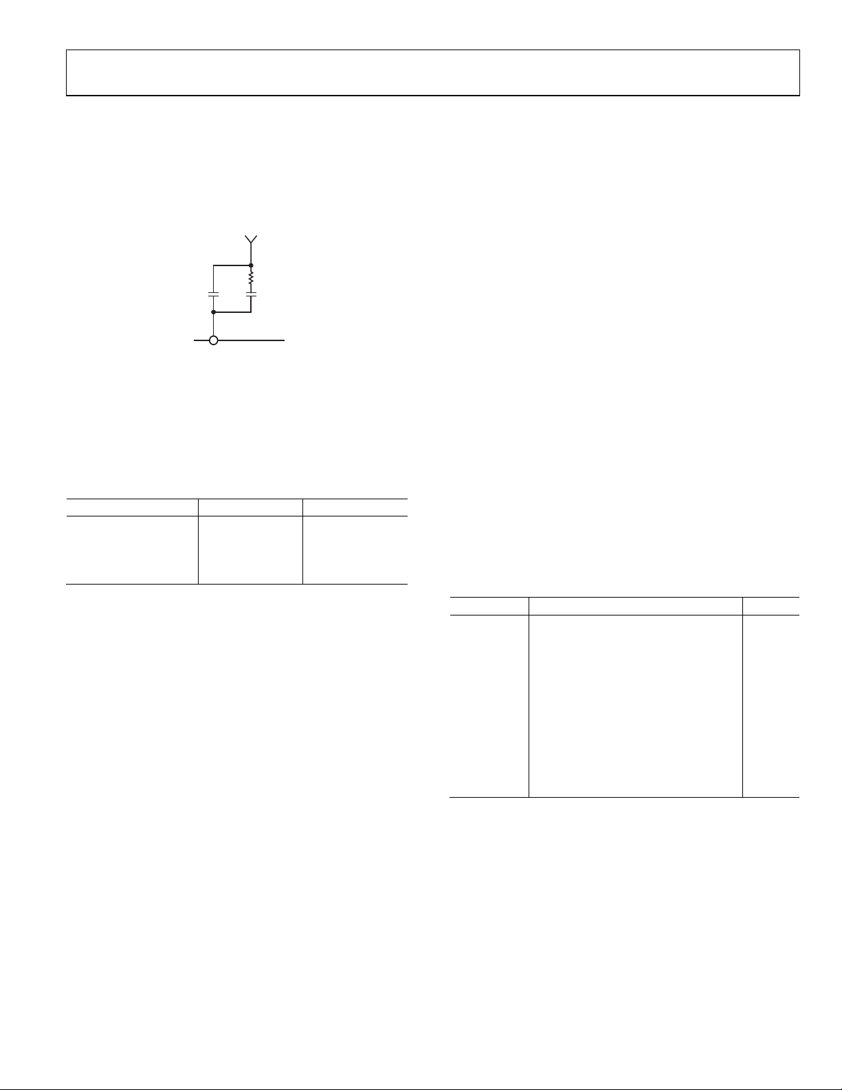
The PLL loop filter should be connected to the PLL_FILT pin. This
filter, shown in Figure 11, includes three passive components—
two capacitors and a resistor. The values of these components
do not need to be exact; the tolerance can be up to 10% for the
resistor and up to 20% for each capacitor. The 3.3 V signal shown
in the schematic can be connected to the PVDD supply of the chip.
PVDD
1.5kΩ
33nF1.8nF
ADAU1445/
ADAU1446
PLL_FILT
Figure 11. PLL Loop Filter
07696-011
Using the ADAU1445/ADAU1446 as Clock Masters
To output a master clock from the ADAU1445/ADAU1446 to
other chips in the system, the CLKOUT pin is used. To set the
frequency of this clock signal, the CLKMODEx pins must be set
(see Tabl e 8).
Table 8. CLKOUT Modes
CLKOUT Signal CLKMODE1 CLKMODE0
Disabled 0 0
Buffered Oscillator 0 1
256 × f
512 × f
1 0
S,NORMAL
1 1
S,NORMAL
Master Clock and PLL Modes and Settings
DSP Core Rate Select Register (Address 0xE220)
The core’s start pulse initiates the operation of the core and
determines the sample rate of signals processed inside the core.
This pulse can originate from one of three internally generated
f
signals (f
S
S,NORMAL
, f
S,DUAL
, or f
), one of the 12 serial input fS
S,QUAD
signals (an LRCLK signal associated with a serial input port),
one of the 12 serial output f
signals (an LRCLK signal associated
S
with a serial output port), or LRCLK recovered from the S/PDIF
receiver input.
Setting the value of the DSP core rate select register sets the speed
of the DSP core (see Ta ble 10). By default, the signals processed
in the core are at the normal DSP core rate; therefore, the core
clock is 3584 × f
. For a system processing signals in the
S, NORMAL
core at the dual rate, the start pulse should be set to the internally
generated dual rate, and the core clock is 1792 × f
S,DUAL
. For a
system processing signals in the core at the quad rate, the start
pulse should be set to the internally generated quad rate, and
the core clock is 896 × f
S,QUAD
.
Master Clock Enable Switch Register (Address 0xE280)
For power-saving purposes, various parts of the chip can be
switched on and off. Setting the appropriate bit to 0 disables the
corresponding subsystem, and setting the bit to 1 enables the
subsystem. This is the first register that should be set after the
device is powered on and completes its initialization. Failure to
set this register may compromise future register writes.
Table 9. Bit Descriptions of Register 0xE280
Bit Position Description
1
Default
[15:9] Reserved
[8] Enable MCLK to auxiliary ADCs 0
[7] Enable MCLK to S/PDIF transmitter 0
[6] Enable MCLK to S/PDIF receiver 0
[5] Enable MCLK to DSP core 0
[4] Enable MCLK to Stereo ASRC[7:4]
[3] Enable MCLK to Stereo ASRC[3:0]
2
2
0
0
[2] Enable MCLK to serial outputs 0
[1] Enable MCLK to serial inputs 0
[0]
Enable MCLK to flexible audio routing
0
matrix (FARM)
1
0 = disable, 1 = enable.
2
See the Flexible Audio Routing Matrix—Input Side section for more
information.
Rev. A | Page 21 of 92

ADAU1445/ADAU1446
Table 10. Bit Descriptions of Register 0xE220
Bit Position Description Default
[15:5] Reserved
[4:0] Start pulse select 00000
00000 = internally generated normal rate (f
00001 = internally generated dual rate (f
00010 = internally generated quad rate (f
00011 = fS from serial input Stereo Pair 0
00100 = fS from serial input Stereo Pair 1
00101 = fS from serial input Stereo Pair 2
00110 = fS from serial input Stereo Pair 3
00111 = fS from serial input Stereo Pair 4
01000 = fS from serial input Stereo Pair 5
01001 = fS from serial input Stereo Pair 6
01010 = fS from serial input Stereo Pair 7
01011 = fS from serial input Stereo Pair 8
01100 = fS from serial input Stereo Pair 9
01101 = fS from serial input Stereo Pair 10
01110 = fS from serial input Stereo Pair 11
S,DUAL
S,QUAD
1
1
1
1
1
1
1
1
1
1
1
1
01111 = fS from serial output Stereo Pair 0
10000 = fS from serial output Stereo Pair 1
10001 = fS from serial output Stereo Pair 2
10010 = fS from serial output Stereo Pair 3
10011 = fS from serial output Stereo Pair 4
10100 = fS from serial output Stereo Pair 5
10101 = fS from serial output Stereo Pair 6
10110 = fS from serial output Stereo Pair 7
10111 = fS from serial output Stereo Pair 8
11000 = fS from serial output Stereo Pair 9
11001 = fS from serial output Stereo Pair 10
11010 = fS from serial output Stereo Pair 11
11011 = fS from S/PDIF receiver
1
fS is the LRCLK of the associated stereo audio pair in the flexible audio routing matrix, whose frequency is dependent on the settings of its associated serial port and
the clock pad multiplexer. The intended function of the DSP core rate select register is to allow the DSP core to be synchronized to an external LRCLK signal that is
being used by any of the serial ports or S/PDIF receiver.
1
)
S,NORMAL
)
)
1
1
1
1
1
1
1
1
1
1
1
1
Rev. A | Page 22 of 92
ADAU1445/ADAU1446
V
VOLTAGE REGULATOR
The digital supply voltage of the ADAU1445/ADAU1446 must
be set to 1.8 V. The chip includes an on-board voltage regulator
that allows the device to be used in systems where a 1.8 V supply is
not available but a 3.3 V supply is. The only external components
needed for this are a PNP transistor and one resistor. Only one
pin, VDRIVE, is necessary to support the regulator.
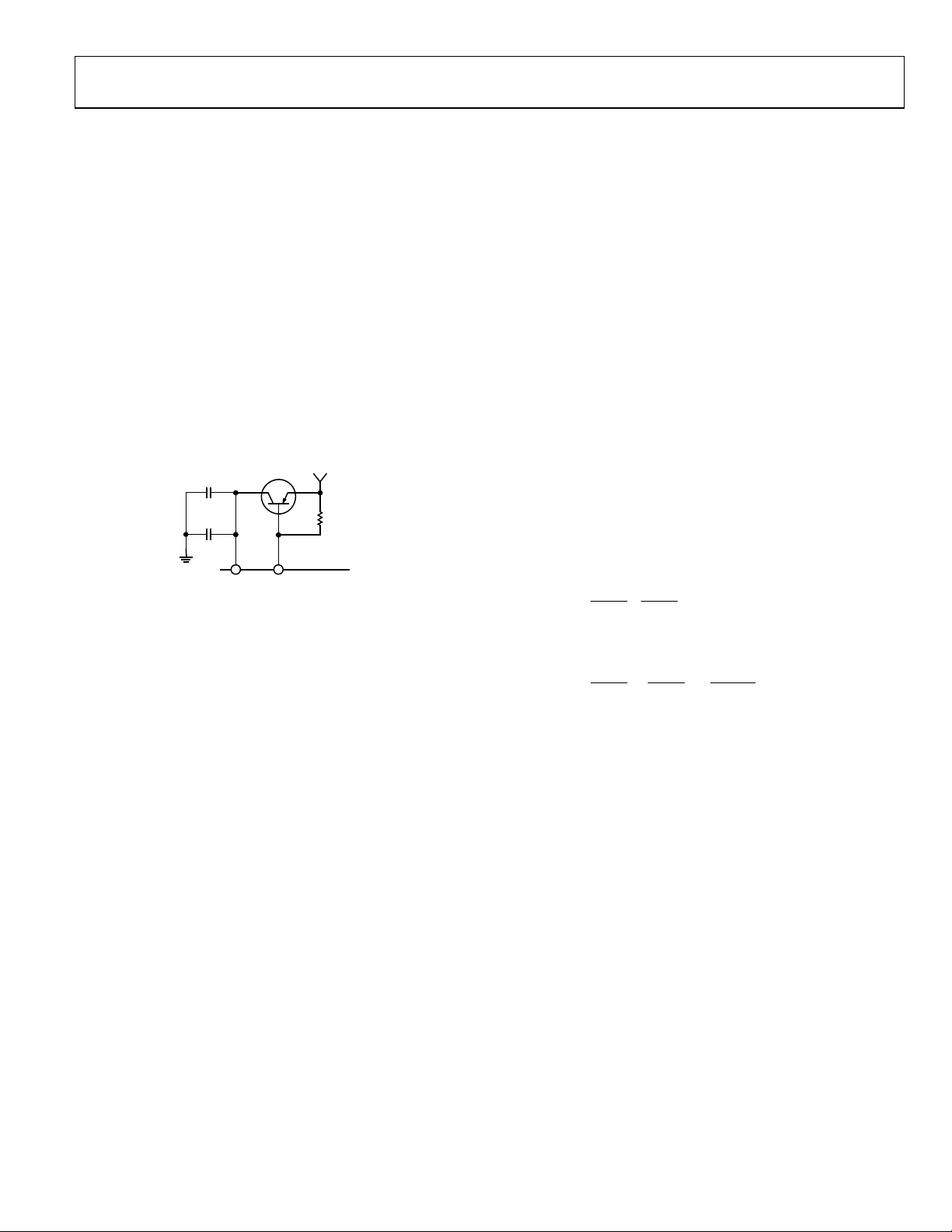
The recommended design for the voltage regulator is shown
in Figure 12. The 10 µF and 100 nF capacitors shown in this
schematic are recommended for bypassing but are not necessary
for operation. Each DVDD pin should have its own 100 nF
bypass capacitor, but only one bulk capacitor (10 µF) is needed
for all pins. In this design, 3.3 V is the main system voltage; 1.8 V
is generated at the collector of the transistor, which is connected
to the DVDD pins. VDRIVE is connected to the base of the PNP
transistor. If the regulator is not used in the design, VDRIVE
can be tied to ground.
10µF
+
100nF
DVDD
VDRIVE
Figure 12. Voltage Regulator Design
3.3
1kΩ
ADAU1445/
ADAU1446
07696-012
Two specifications must be considered when choosing a
regulator transistor. First, the transistor’s current amplification
factor (hFE or beta) should be at least 200. Second, the collector
of the transistor must be able to dissipate the heat generated when
regulating from 3.3 V to 1.8 V. The maximum digital current
draw of the ADAU1445, which uses ASRCs, is 310 mA. The
equation to determine the transistor’s minimum power
dissipation specifications is as follows:
(3.3 V − 1.8 V) × 310 mA = 465 mW
Many transistors fit these specifications. Analog Devices
recommends the NJT4030P from On Semiconductor. For
projects with stringent size constraints, an FMMT734 from
Zetex can be used.
The ADAU1446, which does not contain ASRCs, has a lower
maximum digital current draw of approximately 235 mA. The
maximum power dissipation of the transistor in this case should
be around 355 mW.
SRC GROUP DELAY
The group delay of the sample rate converter is dependent on
the input and output sampling frequencies as described in the
following equations.
For f
For f
S_OUT
GDS
S_OUT
> f
< f
S_IN
S_IN
,
,
3216
+=
ff
INSINS
__
⎛
3216
GDS
GDS is the group delay in seconds.
where
⎜
+=
⎜
ff
INSINS
__
⎝
⎛
⎞
⎜
⎟
×
⎟
⎜
⎠
⎝
⎞
f
_
INS
⎟
⎟
f
OUTS
_
⎠
Rev. A | Page 23 of 92

ADAU1445/ADAU1446
CONTROL PORT
Overview
The ADAU1445/ADAU1446 can operate in one of three control
modes: I
(no external controller).
The ADAU1445/ADAU1446 have both a 4-wire SPI control port
and a 2-wire I
RAMs and registers. When the SELFBOOT pin is low at power-up,
the chip defaults to I
by pulling Pin CLATCH low three times. When the SELFBOOT
pin is set high at power-up, the ADAU1445/ADAU1446 load
the program, parameters, and register settings from an external
EEPROM at startup.
The control port is capable of full read and write operations for
all memories and registers, except for those that are read only.
Most signal processing parameters are controlled by writing
new values to the parameter RAM using the control port. Other
functions, such as mute and input/output mode control, are
programmed by writing to the registers.
All addresses can be accessed in either a single-word mode or a
burst mode. A control word consists of the chip address, the
register/RAM subaddress, and the data to be written. The
number of bytes per word depends on the type of data that is
being written.
The first byte (Byte 0) of a control word contains the 7-bit chip
address plus the R/
together form the subaddress of the memory or register location
within the ADAU1445/ADAU1446. This subaddress must be
two bytes because the memory locations within the ADAU1445/
ADAU1446 are directly addressable, and their sizes exceed the
range of single-byte addressing. All subsequent bytes (starting
with Byte 3) contain the data, such as control port data, program
data, or parameter data. The exact formats for specific types of
writes are shown in and . Figure 13 Figure 19
The ADAU1445/ADAU1446 have several mechanisms for
updating signal processing parameters in real time without causing
pops or clicks on the output. In cases where large blocks of data
must be downloaded, the output of the DSP core can be halted,
new data can be loaded, and then the output of the DSP core can be
restarted. This is typically done during the booting sequence at
startup or when loading a new program into RAM. In cases
where only a few parameters must be changed, they can be
loaded without halting the program. A software-based safeload
mechanism is included for this purpose, and it can be used to
buffer a full set of parameters (for example, the five coefficients
of a biquad) and then transfer these parameters into the active
program within one audio frame.
The control port pins are multifunctional according to the
mode in which the part is operating. Ta b le 1 4 details these
functions.
2
C control mode, SPI control mode, or self-boot mode
2
C bus control port. Each can be used to set the
2
C mode but can be put into SPI control mode
bit. The next two bytes (Byte 1 and Byte 2)
W
I2C Port
The ADAU1445/ADAU1446 support a 2-wire serial (I2C
compatible) microprocessor bus driving multiple peripherals.
Two pins, serial data (SDA) and serial clock (SCL), carry information between the ADAU1445/ADAU1446 and the system I
2
master controller. In I
C mode, the ADAU1445/ADAU1446 are
2
always slaves on the bus, which means that the parts cannot initiate
a data transfer.
Each slave device is recognized by a unique address. The address
bit sequence is shown in Ta b le 1 1 . The ADAU1445/ADAU1446
have eight possible slave addresses: four for writing operations
and four for reading. These are unique addresses for the device
and are illustrated in Tabl e 12 .
Users can communicate with these addresses by using the USBi
communication channel list in the hardware configuration tab
of SigmaStudio. The LSB of the byte sets either a read or write
operation; Logic Level 1 corresponds to a read operation, and
Logic Level 0 corresponds to a write operation. Address Bit 5 and
Address Bit 6 are set by tying the ADDRx pins of the ADAU1445/
ADAU1446 to Logic Level 0 or Logic Level 1. Both SDA and
SCL should have pull-up resistors on the lines connected to them
(a standard value is 2.0 kΩ, but this can be changed depending
on the capacitive load on the line). The voltage on these signal
lines should not be greater than the voltage of IOVDD (3.3 V).
Table 11. ADAU1445/ADAU1446 Address Bit Sequence
Bit 0 Bit 1 Bit 2 Bit 3 Bit 4 Bit 5 Bit 6 Bit 7
0 1 1 1 0 ADDR1 ADDR0
R/W
Table 12. ADAU1445/ADAU1446 I2C Slave Addresses
ADDR1 ADDR0 Read/Write1 Slave Address
0 0 0 0x70
0 0 1 0x71
0 1 0 0x72
0 1 1 0x73
1 0 0 0x74
1 0 1 0x75
1 1 0 0x76
1 1 1 0x77
1
0 = write, 1 = read.
Addressing
Initially, all devices on the I2C bus are in an idle state, in which
the devices monitor the SDA and SCL lines for a start condition
2
and the proper address. The I
C master initiates a data transfer by
establishing a start condition, defined by a high-to-low transition
on SDA while SCL remains high. This indicates that an address or
an address and data stream follow. All devices on the bus respond
to the start condition and shift the next eight bits (7-bit address
bit) MSB first. The device that recognizes the transmitted
+ R/
W
address responds by pulling the data line low during the ninth
clock pulse. This ninth bit is known as an acknowledge bit. All
other devices withdraw from the bus at this point and return to
C
Rev. A | Page 24 of 92
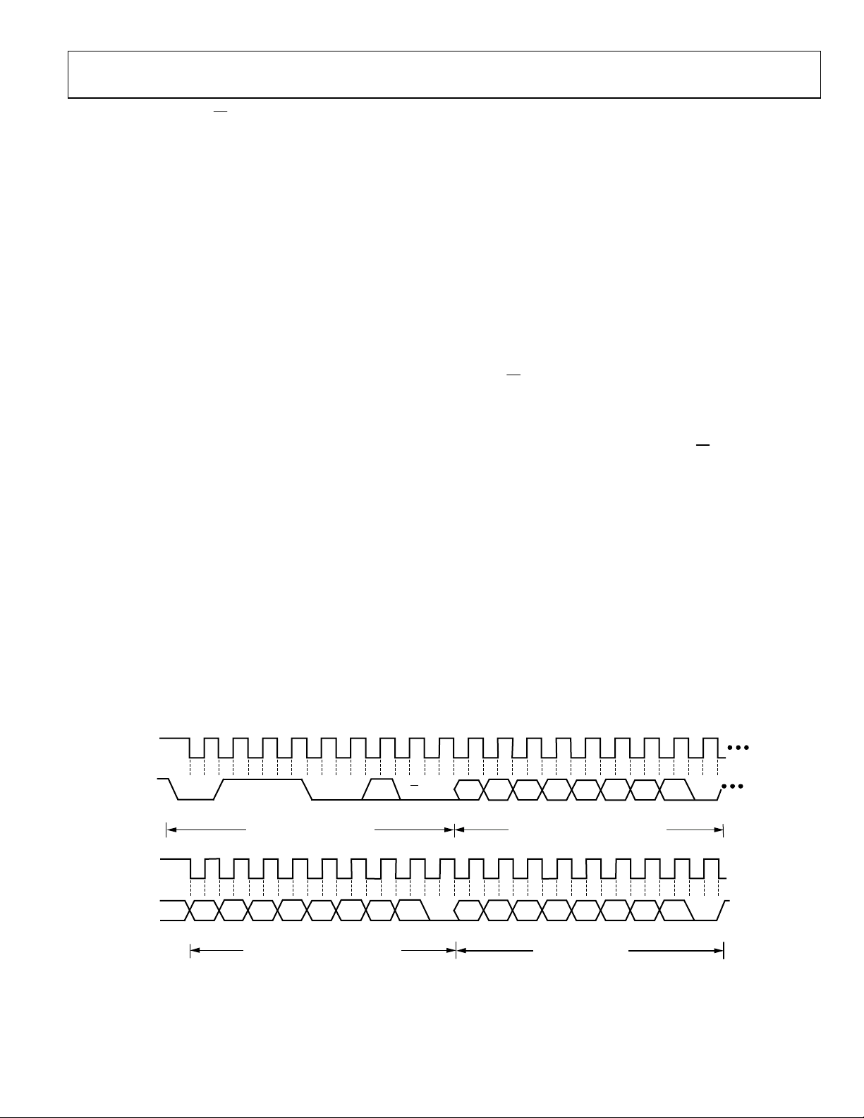
ADAU1445/ADAU1446
(
(
the idle condition. The R/W bit determines the direction of the
data. A Logic 0 on the LSB of the first byte means that the master
writes information to the peripheral. A Logic 1 on the LSB of
the first byte means that the master reads information from the
peripheral. A data transfer takes place until a stop condition is
encountered. A stop condition occurs when SDA transitions
from low to high while SCL is held high. shows the
2
timing of an I
C write.
Figure 13
Burst mode addressing, where the subaddresses are automatically
incremented at word boundaries, can be used for writing large
amounts of data to contiguous memory locations. This increment
happens automatically, unless a stop condition is encountered after
a single-word write. The registers and RAMs in the ADAU1445/
ADAU1446 range in width from one to five bytes; therefore, the
auto-increment feature knows the mapping between subaddresses
and the word length of the destination register (or memory location). A data transfer is always terminated by a stop condition.
Stop and start conditions can be detected at any stage during the
data transfer. If these conditions are asserted out of sequence
with normal read and write operations, they cause an immediate
jump to the idle condition. During a given SCL high period, the
user should only issue one start condition, one stop condition, or a
single stop condition followed by a single start condition. If an invalid subaddress is issued by the user, the ADAU1445/ADAU1446
do not issue an acknowledge and return to the idle condition. If
the user exceeds the highest subaddress while in auto-increment
mode, one of two actions is taken. In read mode, the ADAU1445/
ADAU1446 output the highest subaddress register contents
until the master device issues a no acknowledge, indicating the
end of a read. A no-acknowledge condition is where the SDA
line is not pulled low on the ninth clock pulse on SCL. If the
highest subaddress location is reached while in write mode, the
data for the invalid byte is not loaded into any subaddress register, a
no acknowledge is issued by the ADAU1445/ADAU1446, and
the part returns to the idle condition.
I2C Read and Write Operations
Figure 15 shows the sequence of a single-word write operation.
Every ninth clock, the ADAU1445/ADAU1446 issue an
acknowledge by pulling SDA low.
Figure 16 shows the sequence of a burst mode write operation.
This figure shows an example in which the target destination
registers are two bytes. The ADAU1445/ADAU1446 know to
increment the subaddress register every two bytes because the
requested subaddress corresponds to a register or memory area
with a 2-byte word length.
The sequence of a single-word read operation is shown in
Figure 17. Note that, even though this is a read operation, the
first R/
bit is a 0, indicating a write operation. This is because
W
the subaddress must be written to set up the internal address.
After the ADAU1445/ADAU1446 acknowledge the receipt of
the subaddress, the master must issue a repeated start command
followed by the chip address byte with the R/
set to 1, indicating
W
a read operation. This causes the SDA pin of the ADAU1445/
ADAU1446 to switch directions and begin driving data back to
the master. The master then responds every ninth pulse with an
acknowledge pulse to the ADAU1445/ADAU1446.
Figure 18 shows the sequence of a burst mode read operation.
This figure shows an example in which the target read registers
are two bytes. The ADAU1445/ADAU1446 increment the
subaddress every two bytes because the requested subaddress
corresponds to a register or memory area with word lengths of
two bytes. Other address ranges can have a variety of word
lengths, ranging from one to five bytes; the ADAU1445/
ADAU1446 always decode the subaddress and set the autoincrement circuit so that the address increments after the
appropriate number of bytes.
SCL
0
SDA
START BY
MASTER
SCL
CONTINUED)
SDA
CONTINUED)
111
CHIPADDRESS BYTE
SUBADDRESS BYTE 2
00
FRAME 1
FRAME 2
ADR
R/W
SEL
ADAU1445/ADAU1446
ADAU1445/ADAU1446
ACK BY
ACK BY
Figure 13. I
2
C Write Clocking
Rev. A | Page 25 of 92
FRAME 2
SUBADDRESS BYTE 1
FRAME 3
DATA BYTE 1
ADAU1445/ADAU1446
ADAU1445/ADAU1446
ACK BY
ACK BY
STOP BY
MASTER
07696-013
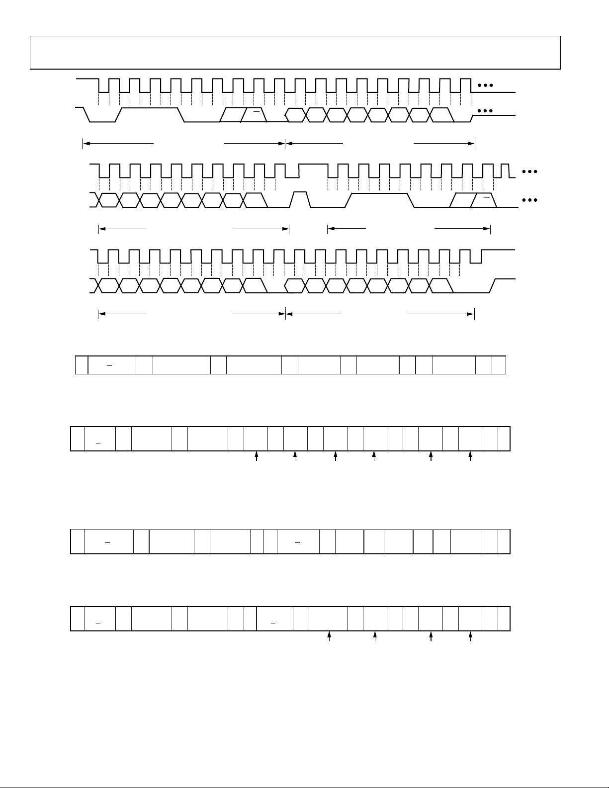
ADAU1445/ADAU1446
SCL
START BY
(CONTINUED)
(CONTINUED)
(CONTINUED)
(CONTINUED)
0
SDA
MASTER
SCL
SDA
SCL
SDA
CHIP ADDRESS,
S
S = START BI T, P = STOP BIT, AM = ACKNO WLEDGE BY MASTER, AS = ACKNOWLEDGE BY S LAVE.
SHOWS A ONE-W O RD W RI TE, WHERE EACH W O RD HAS N BYTE S.
111
R/W = 0
CHIP ADDRESS BYTE
SUBADDRESS BYTE 2
READ DATA BYTE 1
SUBADDRESS,
AS
00
FRAME 1
FRAME 3
FRAME 5
HIGH
ADR
R/W
SEL
ADAU1445/ADAU1446
ADAU1445/ADAU1446
AS AS AS AS ... AS P
Figure 15. Single-Word I
ACK BY
ACK BY
ACK BY
MASTER
Figure 14. I
SUBADDRESS,
LOW
REPEATED
START BY
MASTER
2
C Read Clocking
DATA
BYTE 1
2
C Write Sequence
FRAME 2
SUBADDRESS BYTE 1
0111
CHIP ADDRESS BYTE
FRAME 6
READ DATA BYTE 2
DATA
BYTE 2
ADAU1445/ADAU1446
FRAME 4
ACK BY
00
ADAU1445/ADAU1446
ACK BY
MASTER
DATA
BYTE N
ADR
SEL
R/W
STOP BY
MASTER
ACK BY
07696-014
07696-015
CHIP
S AS AS ASASASASAS ASAS
ADDRESS,
R/W = 0
S = START BI T, P = STOP BIT, AM = ACKNO WLEDGE BY M AS T ER, AS = ACKNOWLEDGE BY SL AV E.
SHOWS AN N-WORD WRITE, WHERE EACH WORD HAS TWO BY TES. (OTHER WORD LE NGTHS ARE POSS IBLE, RANGING FROM ONE TO FIVE BYTES.)
SUBADDRESS,
HIGH
SUBADDRESS,
LOW
DATA-WO RD 1 ,
BYTE 1
DATA-WORD 1,
BYTE 2
Figure 16. Burst Mode I
DATA-WO RD 2,
BYTE 1
2
C Write Sequence
DATA-WO RD 2 ,
BYTE 2
...
DATA-WO RD N,
BYTE 1
DATA-WO RD N ,
BYTE 2
P
7696-016
CHIP ADDRESS,
S
R/W = 0
S = START BIT, P = ST OP BIT, AM = ACKNOWLEDGE BY M AS TER, AS = ACKNOWLEDGE BY SLAVE.
SHOWS A ONE- WORD WRIT E , WHERE EACH WORD HAS N BYTES.
SUBADDRESS,
HIGH
SUBADDRESS,
LOW
Figure 17. Single-Word I
CHIP ADDRESS,
R/W = 1
2
C Read Sequence
DATA
BYTE 1
DATA
BYTE 2
DATA
...
AMAMAS AMAS SASAS
BYTE N
P
7696-017
CHIP
SAS AS AS AS AMAM AMAM
ADDRESS,
R/W = 0
S = START BIT, P = ST OP BIT, AM = ACKNOWLEDGE BY M AS TER, AS = ACKNOWLEDGE BY SLAVE.
SHOWS AN N-WORD WRITE, WHERE EACH WO RD HAS TWO BYTE S . (OTHER W ORD LENGTHS ARE POSSIBLE, RANGING FROM ONE TO FIVE BYTES.)
SUBADDRESS,
HIGH
SUBADDRESS,
LOW
Figure 18. Burst Mode I
S
CHIP
ADDRESS,
R/W = 1
DATA-WORD 1,
BYTE 1
2
C Read Sequence
DATA-WO RD 1 ,
BYTE 2
...
DATA-WO RD N,
BYTE 1
DATA-WO RD N,
BYTE 2
P
07696-018
Rev. A | Page 26 of 92
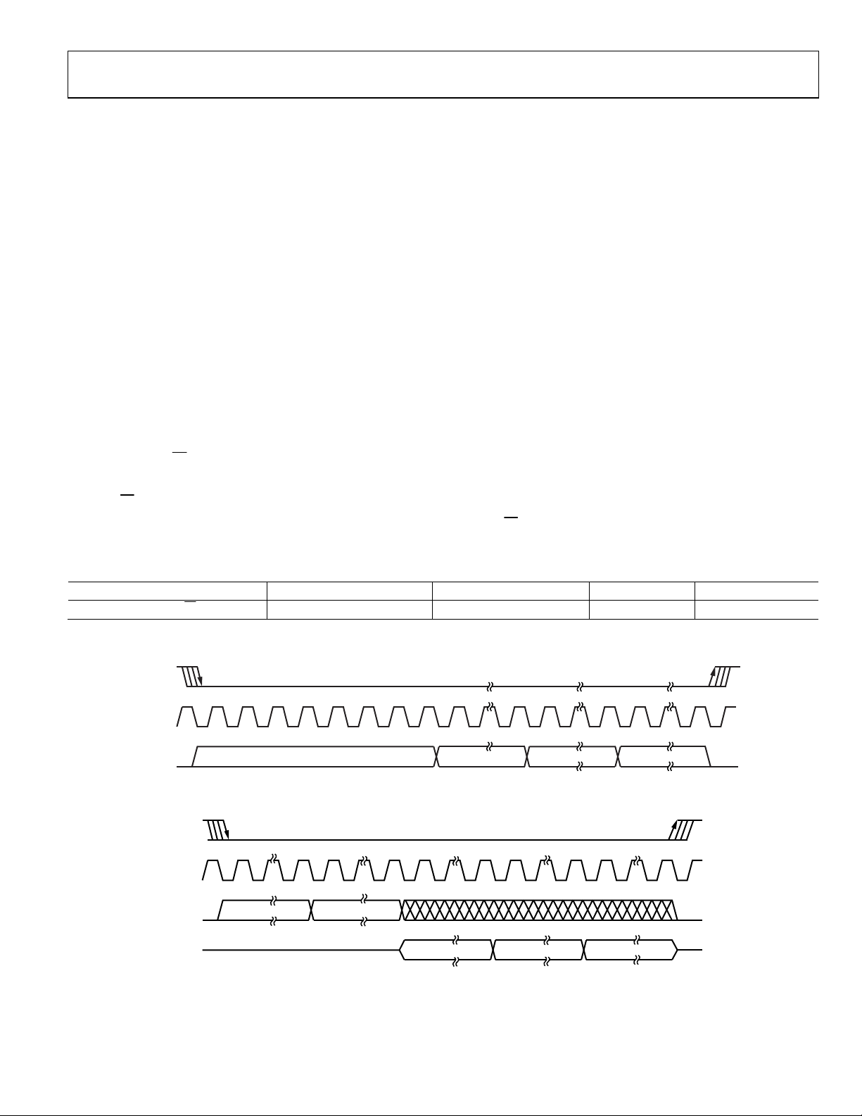
ADAU1445/ADAU1446
SPI Port
By default, the ADAU1445/ADAU1446 are in I2C mode, but
these parts can be put into SPI control mode by pulling CLATCH
low three times. Each low pulse should have a minimum duration
of 20 ns, and the delay between pulses should be at least 20 ns.
The SPI port uses a 4-wire interface, consisting of CLATCH,
CCLK, CDATA, and COUT signals. The CLATCH signal goes
low at the beginning of a transaction and high at the end of a
transaction. The CCLK signal latches CDATA on a low-to-high
transition. COUT data is shifted out of the ADAU1445/ADAU1446
on the falling edge of CCLK and should be clocked into a receiving
device, such as a microcontroller, on the next CCLK falling edge
(rising edge is possible if t
timing is met). The CDATA signal
COV
carries the serial input data, and the COUT signal is the serial
output data. The COUT signal remains three-stated until a read
operation is requested. This allows other SPI-compatible peripherals to share the same readback line. All SPI transactions have
the same word sequence shown in Tabl e 13 (see Figure 4 for an
SPI port timing diagram). All data written should be MSB first.
Chip Address R/W
The first byte of an SPI transaction includes the 7-bit chip address
and a R/
bit. The chip address is set by the ADDR0 pin. This
W
allows two ADAU1445/ADAU1446 devices to share a CLATCH
signal, yet still operate independently. When ADDR0 is low, the
chip address is 0000000; when ADDR0 is high, the address is
0000001. The LSB of the first byte determines whether the SPI
transaction is a read (Logic Level 1) or a write (Logic Level 0).
Users can communicate with both ICs with up to five latch signals
by using the USBi communication channel list in the hardware
configuration tab in SigmaStudio.
Subaddress
The 16-bit subaddress word is decoded into a location in one of
the memories or registers. This subaddress is the location of the
appropriate RAM location or register.
Data Bytes
The number of data bytes varies according to the register or
memory being accessed. In burst write mode, an initial
subaddress is given followed by a continuous sequence of data
for consecutive memory or register locations. The detailed data
format for continuous mode operation is shown in Figure 4.
A sample timing diagram for a single SPI write operation to the
parameter RAM is shown in Figure 19. A sample timing
diagram of a single SPI read operation is shown in Figure 20.
The COUT pin goes from three-state to driven at the beginning
of Byte 3. In this example, Byte 0 to Byte 2 contain the addresses
and R/
bit, and subsequent bytes carry the data.
W
Table 13. Generic Control Word Sequence
Byte 0 Byte 1 Byte 2 Byte 3 Byte 4
Chip Address[6:0], R/W
1
Continues to end of data.
Subaddress[15:8] Subaddress[7:0] Data Data
CLATCH
CCLK
CDATA
Figure 19. SPI Write Clocking (Single-Write Mode)
BYTE 3BYTE 2BYTE 0 BYTE 1
CLATCH
CCLK
CDATA
COUT
BYTE 0
HIGH-Z
BYTE 1
DATA
Figure 20. SPI Read Clocking (Single-Read Mode)
DATA DATA
HIGH-Z
7696-020
1
07696-019
Rev. A | Page 27 of 92

ADAU1445/ADAU1446
Self-Boot
On power-up, the ADAU1445/ADAU1446 can load a program
and a set of parameters that are saved in an external EEPROM.
Combined with the auxiliary ADC and the multipurpose pins,
this can potentially eliminate the need for a microcontroller in a
simple audio system. The self-boot sequence is accomplished by
2
the ADAU1445/ADAU1446 acting as masters on the I
C bus on
startup, which occurs when the SELFBOOT pin is set high. The
ADAU1445/ADAU1446 cannot self-boot in SPI mode.
The maximum necessary EEPROM size is 40,960 bytes, or
40 kB. This much memory is only needed if the program RAM
(4096 × 6 bytes) and parameter RAM (4096 × 4 bytes) are each
completely full.
A self-boot operation is triggered on the rising edge of
RESET
when the SELFBOOT pin is set high, and it occurs after 10 ms
when the PLL has locked. The ADAU1445/ADAU1446 read the
program, parameter, and register data from the EEPROM. After
the ADAU1445/ADAU1446 have finished self-booting, additional
2
messages can be sent to the ADAU1445/ADAU1446 on the I
C
bus, although this typically is not necessary in a self-booting
2
application. The I
C device address for the ADAU1445/ADAU1446
is 0x68 for a write and 0x69 for a read in this mode. The ADDRx
pins have different functions when the chip is in this mode;
therefore, the settings on them are ignored.
2
The ADAU1445/ADAU1446 are masters on the I
C bus during
a self-boot operation. Care should be taken that no other device
2
on the I
booting. The ADAU1445/ADAU1446 generate SCL at 8 × f
therefore, when f
has a duty cycle of ⅜ in accordance with the I
C bus tries to perform a write operation during self-
is 48 kHz, SCL runs at 384 kHz. SCL
s,NORMAL
2
C specification.
;
s
The ADAU1445/ADAU1446 read from EEPROM Chip Address
0xA1. The LSBs of the addresses of some EEPROMs are pin configurable; in most cases, these pins should be tied low to set this
address. SigmaStudio writes to the EEPROM at Address 0xA0.
EEPROM Format
The EEPROM data contains a sequence of messages. Each
discrete message is one of the four types defined in Tabl e 15.
Each message consists of a sequence of one or more bytes. The
first byte identifies the message type. Bytes are written MSB
first. Most messages are block write (0x01) types, which are
used for writing to the ADAU1445/ADAU1446 program RAM,
parameter RAM, and control registers.
The body of the message following the message type should
start with a byte indicating message length and then include a
byte indicating the chip address. Following this is always a
2-byte register or memory address field, as with all other
control port transactions.
SigmaStudio is capable of generating the EEPROM data necessary
to self-boot the ADAU1445/ADAU1446, using the function
called write latest compilation to E2PROM. This function can
be accessed by right-clicking the ADAU1445/ADAU1446 IC in
the hardware configuration window.
Table 14. Functions of the Control Port Pins
Pin I2C Mode SPI Mode Self-Boot
SCL/CCLK SCL—input CCLK—input SCL—output
SDA/COUT SDA—open collector output COUT—output SDA—open collector output
ADDR1/CDATA ADDR1—input CDATA—input Unused input—tie to ground or power
CLATCH Unused input—tie to ground or power CLATCH—input Unused input—tie to ground or power
ADDR0 ADDR0—input ADDR0—input Unused input—tie to ground or power
Table 15. EEPROM Message Types
Message ID Message Type Following Bytes
0x00 End None
0x01 Write
0x02 Delay Two bytes for delay
0x03 No op None
One byte indicating message length (including chip address and
subaddress), one byte indicating chip address, two bytes
indicating subaddress, and an appropriate number of data bytes
Rev. A | Page 28 of 92
 Loading...