
SigmaDSP 28-/56-Bit Audio Processor
www.BDTIC.com/ADI
FEATURES
28-/56-bit, 50 MIPS digital audio processor
2 ADCs: SNR of 100 dB, THD + N of −83 dB
4 DACs: SNR of 104 dB, THD + N of −90 dB
Complete standalone operation
Self-boot from serial EEPROM
Auxiliary ADC with 4-input mux for analog control
GPIOs for digital controls and outputs
Fully programmable with SigmaStudio graphical tool
28-bit × 28-bit multiplier with 56-bit accumulator for full
double-precision processing
Clock oscillator for generating master clock from crystal
PLL for generating master clock from 64 × f
384 × f
Flexible serial data input/output ports with I
left-justified, right-justified, and TDM modes
Sampling rates of up to 192 kHz supported
On-chip voltage regulator for compatibility with 3.3 V systems
48-lead, plastic LQFP
, or 512 × fS clocks
S
APPLICATIONS
Multimedia speaker systems
MP3 player speaker docks
Automotive head units
Minicomponent stereos
Digital televisions
Studio monitors
Speaker crossovers
Musical instrument effects processors
In-seat sound systems (aircraft/motor coaches)
, 256 × fS,
S
2
S-compatible,
with Two ADCs and Four DACs
ADAU1401
GENERAL DESCRIPTION
The ADAU1401 is a complete single-chip audio system with a
28-/56-bit audio DSP, ADCs, DACs, and microcontroller-like
control interfaces. Signal processing includes equalization, cross
over, bass enhancement, multiband dynamics processing, delay
compensation, speaker compensation, and stereo image widening.
This processing can be used to compensate for real-world limitations of speakers, amplifiers, and listening environments,
providing dramatic improvements in perceived audio quality.
Its signal processing is comparable to that found in high end
studio equipment. Most processing is done in full 56-bit, double
precision mode, resulting in very good low level signal performance. The ADAU1401 is a fully programmable DSP. The easy
to use SigmaStudio™ software allows the user to graphically
configure a custom signal processing flow using blocks such as
biquad filters, dynamics processors, level controls, and GPIO
interface controls.
ADAU1401 programs can be loaded on power-up either from a
serial EEPROM through its own self-boot mechanism or from
an external microcontroller. On power-down, the current state
of the parameters can be written back to the EEPROM from the
ADAU1401 to be recalled the next time the program is run.
Two Σ-Δ ADCs and four Σ-Δ DACs provide a 98.5 dB analog
input to analog output dynamic. Each ADC has a THD + N of
−83 dB, and each DAC has a THD + N of −90 dB. Digital input
and output ports allow a glueless connection to additional
ADCs and DACs. The ADAU1401 communicates through an
2
I
C® bus or a 4-wire SPI port.
Rev. A
Information furnished by Analog Devices is believed to be accurate and reliable. However, no
responsibility is assumed by Analog Devices for its use, nor for any infringements of patents or other
rights of third parties that may result from its use. Specifications subject to change without notice. No
license is granted by implication or otherwise under any patent or patent rights of Analog Devices.
Trademarks and registered trademarks are the property of their respective owners.
One Technology Way, P.O. Box 9106, Norwood, MA 02062-9106, U.S.A.
Tel: 781.329.4700 www.analog.com
Fax: 781.461.3113 ©2007–2008 Analog Devices, Inc. All rights reserved.

ADAU1401
www.BDTIC.com/ADI
TABLE OF CONTENTS
Features .............................................................................................. 1
Applications ....................................................................................... 1
General Description ......................................................................... 1
Revision History ............................................................................... 3
Functional Block Diagram .............................................................. 4
Specifications ..................................................................................... 5
Analog Performance .................................................................... 5
Digital Input/Output .................................................................... 7
Power .............................................................................................. 7
Temperature Range ...................................................................... 7
PLL and Oscillator ........................................................................ 7
Regulator ........................................................................................ 8
Digital Timing Specifications ..................................................... 8
Absolute Maximum Ratings .......................................................... 11
Thermal Resistance .................................................................... 11
ESD Caution ................................................................................ 11
Pin Configuration and Function Descriptions ........................... 12
Typical Performance Characteristics ........................................... 15
System Block Diagram ................................................................... 16
Theory of Operation ...................................................................... 17
Initialization .................................................................................... 18
Power-Up Sequence ................................................................... 18
Control Registers Setup ............................................................. 18
Recommended Program/Parameter Loading Procedure ..... 18
Power Reduction Modes ............................................................ 18
Using the Oscillator .................................................................... 19
Setting Master Clock/PLL Mode .............................................. 19
Voltage Regulator ....................................................................... 20
Audio ADCs .................................................................................... 21
Audio DACs .................................................................................... 22
Control Ports ................................................................................... 23
I2C Port ........................................................................................ 24
SPI Port ........................................................................................ 27
Self-Boot ...................................................................................... 28
Signal Processing ............................................................................ 30
Numeric Formats ........................................................................ 30
Programming .............................................................................. 30
RAMs and Registers ....................................................................... 31
Address Maps .............................................................................. 31
Parameter RAM .......................................................................... 31
Data RAM ................................................................................... 31
Read/Write Data Formats ......................................................... 31
Control Register Map ..................................................................... 33
Control Register Details ................................................................ 35
2048 to 2055 (0x0800 to 0x0807)—Interface Registers ......... 35
2056 (0x808)—GPIO Pin Setting Register .............................. 36
2057 to 2060 (0x809 to 0x80C)—Auxiliary ADC Data
Registers ....................................................................................... 37
2064 to 2068 (0x0810 to 0x814)—Safeload Data Registers .. 38
2069 to 2073 (0x0815 to 0x819)—Safeload Address Registers
....................................................................................................... 38
2074 to 2075 (0x081A to 0x081B)—Data Capture Registers 39
2076 (0x081C)—DSP Core Control Register ......................... 40
2078 (0x081E)—Serial Output Control Register ................... 41
2079 (0x081F)—Serial Input Control Register ....................... 42
2080 to 2081 (0x0820 to 0x0821)—Multipurpose Pin
Configuration Registers ............................................................. 43
2082 (0x0822)—Auxiliary ADC and Power Control ............ 44
2084 (0x0824)—Auxiliary ADC Enable .................................. 44
2086 (0x0826)—Oscillator Power-Down ................................ 44
2087 (0x0827)—DAC Setup ...................................................... 44
Multipurpose Pins .......................................................................... 45
Auxiliary ADC ............................................................................ 45
General-Purpose Input/Output Pins ....................................... 45
Serial Data Input/Output Ports ................................................ 45
Layout Recommendations ............................................................. 48
Parts Placement .......................................................................... 48
Grounding ................................................................................... 48
Typical Application Schematics .................................................... 49
Self-Boot Mode ........................................................................... 49
I2C Control .................................................................................. 50
SPI Control .................................................................................. 51
Outline Dimensions ....................................................................... 52
Ordering Guide .......................................................................... 52
Rev. A | Page 2 of 52

ADAU1401
www.BDTIC.com/ADI
REVISION HISTORY
4/08—Rev. 0 to Rev. A
Changes to Figure 1 ........................................................................... 4
Changes to Table 11 ........................................................................ 12
Replaced Figure 8 to Figure 11 ...................................................... 15
Renamed Theory of Operation Section ...................................... 17
Changes to Initialization Section .................................................. 18
Change to Setting the Master Clock/PLL Mode Section ........... 19
Replaced Figure 22 through Figure 25 ......................................... 26
Changes to EEPROM Format Section .......................................... 28
Deleted Table 21, Renumbered Sequentially ............................... 29
Inserted Figure 28, Renumbered Sequentially ............................ 29
Changes to Figure 37 ...................................................................... 49
Changes to Figure 38 ...................................................................... 50
Changes to Figure 39 ...................................................................... 51
7/07—Revision 0: Initial Version
Rev. A | Page 3 of 52
ADAU1401
www.BDTIC.com/ADI
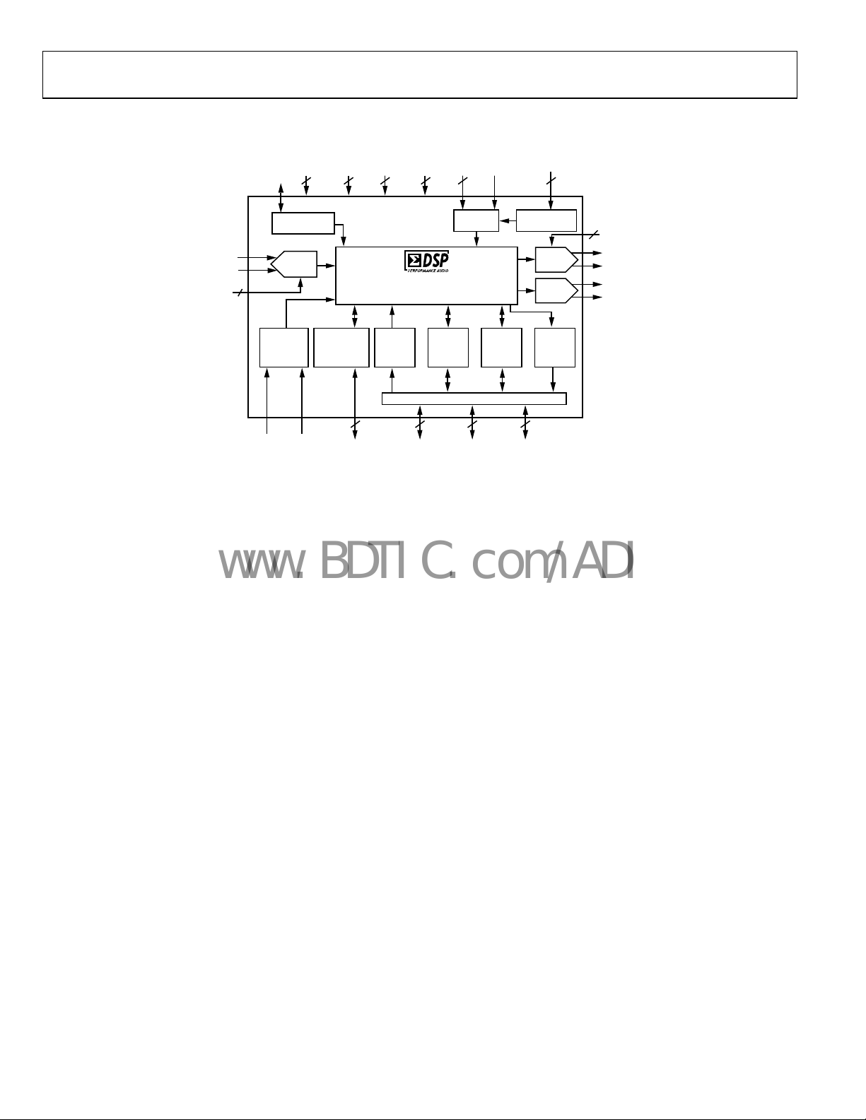
FUNCTIONAL BLOCK DIAGRAM
DIGITAL
DIGITAL
ANALOG
VDD
3.3V
GROUND
3 3 3 2 23
VDD
ANALOG
GROUND
PLL
MODE
PLL LOOP
FILTER
CRYSTAL
OSCILLATOR
GPIO
DIGITAL OUT
OR GPIO
CLOCK
DAC
DAC
8-CH
DIGITAL
OUTPUT
3335
FILTD/ CM
2
4-CHANNEL
ANALOG
OUTPUT
06752-001
2-CHANNEL
ANALOG
INPUT
FILTA/
ADC_RES
2
RESET
1.8V
REGULATOR
STEREO
ADC
RESET/
MODE
SELECT
SELFBOOT
ADAU1401
AUDIO PROCESS OR CORE
CONTROL
INTERFACE
AND
SELFBOOT
2
I
C/SPI
AND WRITEBACK
28-/56-BIT, 50MIPS
40ms DELAY MEMO RY
8-CH
DIGITAL
INPUT
8-BIT
AUX
ADC
INPUT/OUTPUT MATRIX
DIGITAL IN
OR GPIO
AUX ADC
OR GPIO
Figure 1.
PLL
Rev. A | Page 4 of 52

ADAU1401
www.BDTIC.com/ADI
SPECIFICATIONS
AVDD = 3.3 V, DVDD = 1.8 V, PVDD = 3.3 V, IOVDD = 3.3 V, master clock input = 12.288 MHz, unless otherwise noted.
ANALOG PERFORMANCE
Specifications are guaranteed at 25°C (ambient).
Table 1.
Parameter Min Typ Max Unit Test Conditions/Comments
ADC INPUTS
Number of Channels 2 Stereo input
Resolution 24 Bits
Full-Scale Input 100 (283) µA rms (µA p-p)
Signal-to-Noise Ratio
Dynamic Range −60 dB with respect to full-scale analog input
Total Harmonic Distortion + Noise −83 dB −3 dB with respect to full-scale analog input
Interchannel Gain Mismatch 25 250 mdB
Crosstalk −82 dB Analog channel-to-channel crosstalk
DC Bias 1.4 1.5 1.6 V
Gain Error −11 +11 %
DAC OUTPUTS
Number of Channels 4 Two stereo output channels
Resolution 24 Bits
Full-Scale Analog Output 0.9 (2.5) V rms (V p-p)
Signal-to-Noise Ratio
Dynamic Range −60 dB with respect to full-scale analog output
Total Harmonic Distortion +
Noise
Crosstalk −100 dB Analog channel-to-channel crosstalk
Interchannel Gain Mismatch 25 250 mdB
Gain Error −10 +10 %
DC Bias 1.4 1.5 1.6 V
VOLTAGE REFERENCE
Absolute Voltage (CM) 1.4 1.5 1.6 V
AUXILIARY ADC
Full-Scale Analog Input 2.8 3.0 3.1 V
INL 0.5 LSB
DNL 1.0 LSB
Offset 15 mV
Input Impedance 17.8 30 42 kΩ
A-Weighted 100 dB
A-Weighted 95 100 dB
A-Weighted 104 dB
A-Weighted 99 104 dB
2 V rms input with 20 kΩ (18 kΩ external + 2 kΩ internal)
series resistor
−90 dB −1 dB with respect to full-scale analog output
Rev. A | Page 5 of 52

ADAU1401
www.BDTIC.com/ADI
Specifications are guaranteed at 130°C (ambient).
Table 2.
Parameter Min Typ Max Unit Test Conditions/Comments
ADC INPUTS
Number of Channels 2 Stereo input
Resolution 24 Bits
Full-Scale Input 100 (283) µA rms (µA p-p)
Signal-to-Noise Ratio
Dynamic Range −60 dB with respect to full-scale analog input
Tot al H a r monic
Distortion + Noise
Interchannel Gain Mismatch 25 250 mdB
Crosstalk −82 dB Analog channel-to-channel crosstalk
DC Bias 1.4 1.5 1.6 V
Gain Error −11 +11 %
DAC OUTPUTS
Number of Channels 4 Two stereo output channels
Resolution 24 Bits
Full-Scale Analog Output 0.9 (2.5) V rms (V p-p)
Signal-to-Noise Ratio
Dynamic Range −60 dB with respect to full-scale analog output
Total Harmonic Distortion +
Noise
Crosstalk −100 dB Analog channel-to-channel crosstalk
Interchannel Gain Mismatch 25 250 mdB
Gain Error −10 +10 %
DC Bias 1.4 1.5 1.6 V
VOLTAGE REFERENCE
Absolute Voltage (CM) 1.4 1.5 1.6 V
AUXILIARY ADC
Full-Scale Analog Input 2.8 3.0 3.1 V
INL 0.5 LSB
DNL 1.0 LSB
Offset 15 mV
Input Impedance 17.8 30 42 kΩ
A-Weighted 100 dB
A-Weighted 92 100 dB
A-Weighted 104 dB
A-Weighted 98 104 dB
2 V rms input with 20 kΩ (18 kΩ external + 2 kΩ internal)
series resistor
−83 dB −3 dB with respect to full-scale analog input
−90 dB −1 dB with respect to full-scale analog output
Rev. A | Page 6 of 52

ADAU1401
www.BDTIC.com/ADI
DIGITAL INPUT/OUTPUT
Table 3.
Parameter Min Typ Max1 Unit Comments
Input Voltage, High (VIH) 2.0 IOVDD V
Input Voltage, Low (VIL) 0.8 V
Input Leakage, High (IIH) 1 µA Excluding MCLKI
Input Leakage, Low (IIL) 1 µA Excluding MCLKI and bidirectional pins
Bidirectional Pin Pull-Up Current, Low 150 µA
MCLKI Input Leakage, High (IIH) 3 µA
MCLKI Input Leakage, Low (IIL) 3 µA
High Level Output Voltage (VOH), IOH = 2 mA 2.0 V
Low Level Output Voltage (VOL), IOL = 2 mA 0.8 V
Input Capacitance 5 pF
GPIO Output Drive 2 mA
1
Maximum specifications are measured across a temperature range of −40°C to +130°C (case), a DVDD range of 1.62 V to 1.98 V, and an AVDD range of 2.97 V to 3.63 V.
POWER
Table 4.
Parameter Min Typ Max
1
Unit
SUPPLY VOLTAGE
Analog Voltage 3.3 V
Digital Voltage 1.8 V
PLL Voltage 3.3 V
IOVDD Voltage 3.3 V
SUPPLY CURRENT
Analog Current (AVDD and PVDD) 50 85 mA
Digital Current (DVDD) 40 60 mA
Analog Current, Reset 35 55 mA
Digital Current, Reset 1.5 4.5 mA
DISSIPATION
Operation (AVDD, DVDD, PVDD)
2
286.5 mW
Reset, All Supplies 118 mW
POWER SUPPLY REJECTION RATIO (PSRR)
1 kHz, 200 mV p-p Signal at AVDD 50 dB
1
Maximum specifications are measured across a temperature range of −40°C to +130°C (case), a DVDD range of 1.62 V to 1.98 V, and an AVDD range of 2.97 V to 3.63 V.
2
Power dissipation does not include IOVDD power because the current drawn from this supply is dependent on the loads at the digital output pins.
TEMPERATURE RANGE
Table 5.
Parameter Min Typ Max Unit
Functionality Guaranteed −40 +105 °C ambient
PLL AND OSCILLATOR
Table 6. PLL and Oscillator1
Parameter Min Typ Max Unit
PLL Operating Range MCLK_Nom − 20% MCLK_Nom + 20% MHz
PLL Lock Time 20 ms
Crystal Oscillator Transconductance (gm) 78 mmho
1
Maximum specifications are measured across a temperature range of −40°C to +130°C (case), a DVDD range of 1.62 V to 1.98 V, and an AVDD range of 2.97 V to 3.63 V.
Rev. A | Page 7 of 52

ADAU1401
www.BDTIC.com/ADI
REGULATOR
Table 7. Regulator1
Parameter Min Typ Max Unit
DVDD Voltage 1.7 1.8 1.84 V
1
Regulator specifications are calculated using a Zetex Semiconductors FZT953 transistor in the circuit.
DIGITAL TIMING SPECIFICATIONS
Table 8. Digital Timing1
Limit
Parameter t
MASTER CLOCK
tMP 36 244 ns MCLKI period, 512 × fS mode
tMP 48 366 ns MCLKI period, 384 × fS mode
tMP 73 488 ns MCLKI period, 256 × fS mode
tMP 291 1953 ns MCLKI period, 64 × fS mode
SERIAL PORT
t
40 ns INPUT_BCLK low pulse width
BIL
t
40 ns INPUT_BCLK high pulse width
BIH
t
10 ns INPUT_LRCLK setup; time to INPUT_BCLK rising
LIS
t
10 ns INPUT_LRCLK hold; time from INPUT_BCLK rising
LIH
t
10 ns SDATA_INx setup; time to INPUT_BCLK rising
SIS
t
10 ns SDATA_INx hold; time from INPUT_BCLK rising
SIH
t
10 ns OUTPUT_LRCLK setup in slave mode
LOS
t
10 ns OUTPUT_LRCLK hold in slave mode
LOH
tTS 5 ns OUTPUT_BCLK falling to OUTPUT_LRCLK timing skew
t
40 ns SDATA_OUTx delay in slave mode; time from OUTPUT_BCLK falling
SODS
t
40 ns SDATA_OUTx delay in master mode; time from OUTPUT_BCLK falling
SODM
SPI PORT
f
CCLK
t
80 ns CCLK pulse width low
CCPL
t
80 ns CCLK pulse width high
CCPH
t
0 ns CLATCH setup; time to CCLK rising
CLS
t
100 ns CLATCH hold; time from CCLK rising
CLH
t
80 ns CLATCH pulse width high
CLPH
t
0 ns CDATA setup; time to CCLK rising
CDS
t
80 ns CDATA hold; time from CCLK rising
CDH
t
101 ns COUT delay; time from CCLK falling
COD
I2C PORT
f
SCL
t
0.6 µs SCL high
SCLH
t
1.3 µs SCL low
SCLL
t
0.6 µs Setup time, relevant for repeated start condition
SCS
t
0.6 µs Hold time; after this period, the first clock is generated
SCH
tDS 100 ns Data setup time
t
300 ns SCL rise time
SCR
t
300 ns SCL fall time
SCF
t
300 ns SDA rise time
SDR
t
300 ns SDA fall time
SDF
t
0.6 Bus-free time; time between stop and start
BFT
t
MIN
Unit Description
MAX
6.25 MHz CCLK frequency
400 kHz SCL frequency
Rev. A | Page 8 of 52
ADAU1401
www.BDTIC.com/ADI
Limit
Parameter t
MULTIPURPOSE PINS AND RESET
t
50 ns GPIO rise time
GRT
t
50 ns GPIO fall time
GFT
t
1.5 × 1/fS µs GPIO input latency; time until high/low value is read by core
GIL
t
20 ns
RLPW
1
All timing specifications are given for the default (I2S) states of the serial input port and the serial output port (see Table 66).
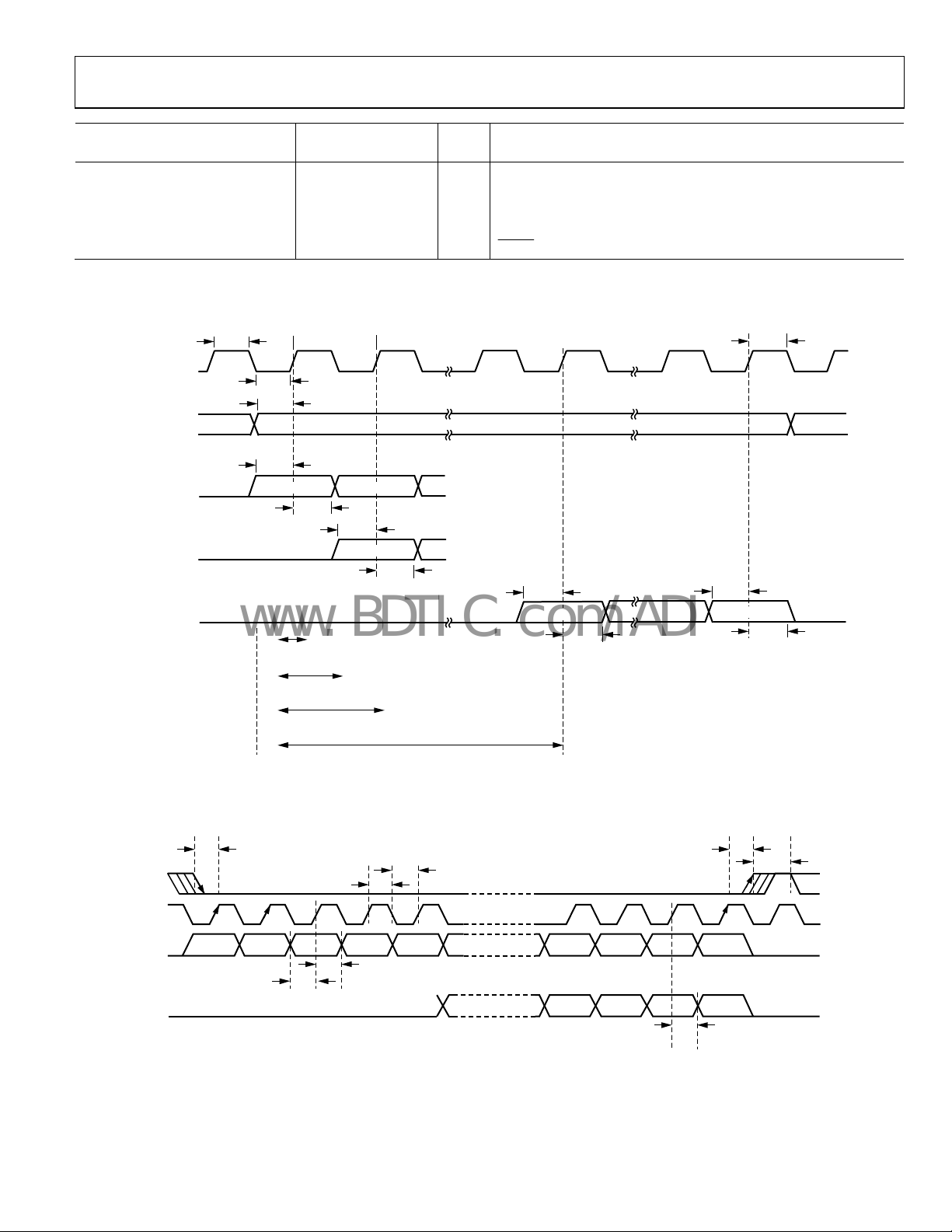
Digital Timing Diagrams
t
BIH
INPUT_BCLK
t
BIL
t
LIS
INPUT_LRCLK
t
SDATA_INx
LEFT-JUSTIFIED
MODE
SDATA_INx
2
I
S MODE
SDATA_INx
RIGHT-JUSTIFIED
MODE
SIS
t
MIN
MSB
t
SIH
8-BIT CLOCKS
(24-BIT DATA)
12-BIT CLOCKS
(20-BIT DATA)
14-BIT CLOCKS
(18-BIT DATA)
16-BIT CLOCKS
(16-BIT DATA)
t
SIS
Unit Description
MAX
MSB–1
MSB
t
SIH
Figure 2. Serial Input Port Timing
RESET
low pulse width
t
SIS
MSB
t
LIH
t
SIS
LSB
t
t
SIH
SIH
06752-002
t
CLS
t
CCPL
CLATCH
CCLK
CDATA
COUT
t
CCPH
t
t
CDS
CDH
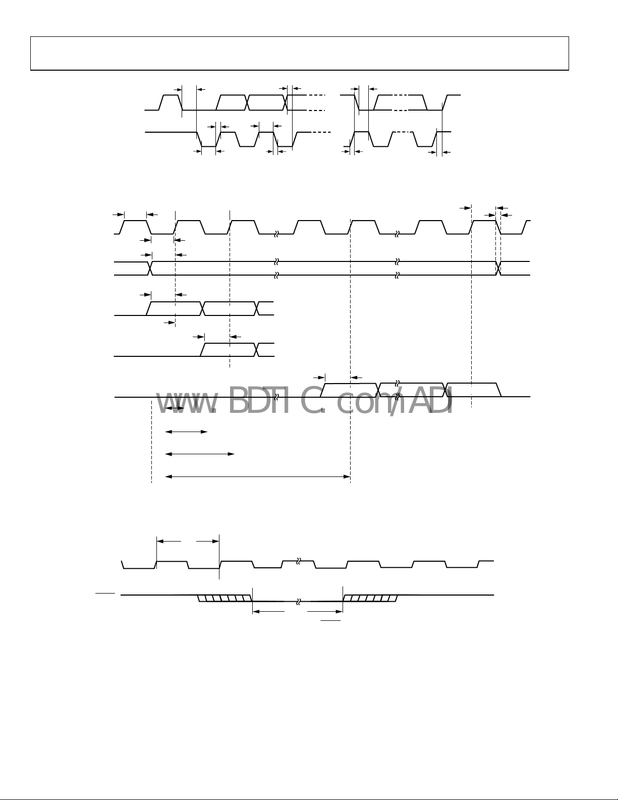
Figure 3. SPI Port Timing
Rev. A | Page 9 of 52
t
CLH
t
COD
t
CLPH
06752-004
ADAU1401
www.BDTIC.com/ADI
t
t
SCLH
DS
t
SCH
SDA
t
SCH
t
SCR
OUTPUT_BCLK
OUTPUT_L RCLK
SDATA_OUTx
LEFT-JUSTIFIED
MODE
SDATA_OUTx
2
S MODE
I
SDATA_OUTx
RIGHT -JUSTI FIED
MODE
SCL
t
BIH
t
BIL
t
LOS
t
SODS
t
SODM
MSB
8-BIT CLOCKS
(24-BIT DATA)
12-BIT CLO CKS
(20-BIT DATA)
14-BIT CLO CKS
(18-BIT DATA)
16-BIT CLO CKS
(16-BIT DATA)
t
SODS
t
SODM
t
t
SCLL
SCF
Figure 4. I
MSB–1
MSB
2
C Port Timing
Figure 5. Serial Output Port Timing
t
SCS
t
t
SODS
SODM
MSB
t
BFT
06752-005
t
LCH
LSB
t
TS
06752-003
t
MP
MCLKI
RESET
t
RLPW
Figure 6. Master Clock and
Rev. A | Page 10 of 52
RESET
06752-006
Timing
ADAU1401
www.BDTIC.com/ADI
ABSOLUTE MAXIMUM RATINGS
Table 9.
Parameter Rating
DVDD to GND 0 V to 2.2 V
AVDD to GND 0 V to 4.0 V
IOVDD to GND 0 V to 4.0 V
Digital Inputs DGND − 0.3 V, IOVDD + 0.3 V
Maximum Junction Temperature 135°C
Storage Temperature Range −65°C to +150°C
Soldering (10 sec) 300°C
Stresses above those listed under Absolute Maximum Ratings
may cause permanent damage to the device. This is a stress
rating only; functional operation of the device at these or any
other conditions above those indicated in the operational
section of this specification is not implied. Exposure to absolute
maximum rating conditions for extended periods may affect
device reliability.
THERMAL RESISTANCE
θJA is specified for the worst-case conditions, that is, a device
soldered in a circuit board for surface-mount packages.
Table 10. Thermal Resistance
Package Type θJA θ
48-Lead LQFP 72 19.5 °C/W
Unit
JC
ESD CAUTION
Rev. A | Page 11 of 52
ADAU1401
www.BDTIC.com/ADI
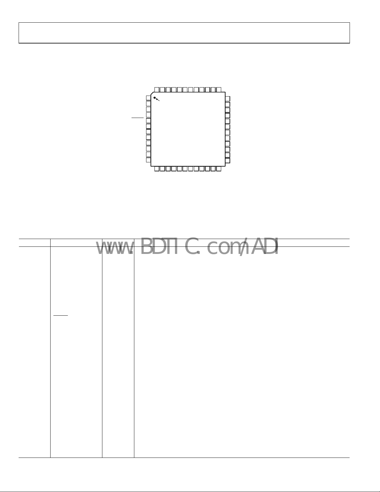
PIN CONFIGURATION AND FUNCTION DESCRIPTIONS
AVDD
FILTA
VOUT0
VOUT1
VOUT2
VOUT3
AGND
FILTDCMPLL_MODE1
PLL_MODE0
AGND
36
AVDD
35
PLL_LF
34
PVDD
33
PG
ND
32
KI
MCL
31
OSCO
30
RSVD
29
MP2
28
MP3
27
MP8
26
MP9
25
DGND
DVDD
SCL/CCLK
SDA/COUT
CLATCH/WP
AGND
ADC1
ADC_RES
ADC0
RESET
SELFBOOT
ADDR0
MP4
MP5
MP1
MP0
DGND
48 47 46 45 44 43 42 41 40 39 38 37
1
PIN 1
INDICATOR
2
3
4
5
6
7
8
9
10
11
12
13 14 15 16 17 18 19 20 21 22 23 24
DVDD
MP7
MP6
ADAU1401
TOP VIEW
(Not to Scale)
MP10
MP11
IOVDD
VDRIVE
Table 11. Pin Function Descriptions
Pin No. Mnemonic Ty pe
1, 37, 42 AGND PWR
1
Description
Analog Ground Pin. The AGND, DGND, and PGND pins can be tied directly together in a
common ground plane. AGND should be decoupled to an AVDD pin with a 100 nF
capacitor.
2 ADC1 A_IN
Analog Audio Input 1. Full-scale 100 A rms input. Current input allows input voltage level
to be scaled with an external resistor. An 18 kΩ resistor gives a 2 V rms full-scale input. See
the Audio ADCs section for details.
3 ADC_RES A_IN
ADC Reference Current. The full-scale current of the ADCs can be set with an external 18 kΩ
resistor connected between this pin and ground. See the Audio ADCs section for details.
4 ADC0 A_IN
Analog Audio Input 0. Full-scale 100 A rms input. Current input allows input voltage level
to be scaled with an external resistor. An 18 kΩ resistor gives a 2 V rms full-scale input.
5
RESET
D_IN
Active Low Reset Input. Reset is triggered on a high-to-low edge, and the ADAU1401 exits
reset on a low-to-high edge. For more information about initialization, see the Power-Up
Sequence section for details.
6 SELFBOOT D_IN
Enable/Disable Self-Boot. SELFBOOT selects control port (low) or self-boot (high). Setting
this pin high initiates a self-boot operation when the ADAU1401 is brought out of a reset. This
pin can be tied directly to the control voltage or pulled up/down with a resistor. See the
Self-Boot section for details.
7 ADDR0 D_IN
2
C and SPI Address 0. In combination with ADDR1, this pin allows up to four ADAU1401s
I
to be used on the same I
signal. See the I
8 MP4 D_IO
Multipurpose GPIO or Serial Input Port LRCLK (INPUT_LRCLK). See the Multipurpose Pins
section for more details.
9 MP5 D_IO
Multipurpose GPIO or Serial Input Port BCLK (INPUT_BCLK). See the Multipurpose Pins
section for more details.
10 MP1 D_IO
Multipurpose GPIO or Serial Input Port Data 1 (SDATA_IN0). See the Multipurpose Pins
section for more details.
11 MP0 D_IO
Multipurpose GPIO or Serial Input Port Data 0 (SDATA_IN1). See the Multipurpose Pins
section for more details.
12, 25 DGND PWR
Digital Ground Pin. The AGND, DGND, and PGND pins can be tied directly together in a
common ground plane. DGND should be decoupled to a DVDD pin with a 100 nF
capacitor.
ADDR1/CDATA/WB
Figure 7. 48-Lead LQFP Pin Configuration
2
2
C Port section for details.
C bus and up to two ICs to be used with a common SPI CLATCH
06752-007
Rev. A | Page 12 of 52
ADAU1401
www.BDTIC.com/ADI
Pin No. Mnemonic Ty pe
13, 24 DVDD PWR
14 MP7 D_IO
15 MP6 D_IO
16 MP10 D_IO
17 VDRIVE A_OUT
18 IOVDD PWR
19 MP11 D_IO
20 ADDR1/CDATA/WB D_IN
CDATA: SPI Data Input. See the SPI Port section for details.
21 CLATCH/WP D_IO
22 SDA/COUT D_IO
23 SCL/CCLK D_IO
26 MP9 D_IO/A_IO
27 MP8 D_IO/A_IO
28 MP3 D_IO/A_IO
29 MP2 D_IO/A_IO
30 RSVD X Reserved. Tie to ground, either directly or through a pull-down resistor.
31 OSCO D_OUT
32 MCLKI D_IN
33 PGND PWR
1
Description
1.8 V Digital Supply. This can be supplied either externally or generated from a 3.3 V
supply with the on-board 1.8 V regulator. DVDD should be decoupled to DGND with a 100
nF capacitor.
Multipurpose GPIO or Serial Output Port Data 1 (SDATA_OUT1). See the Multipurpose Pins
section for more details.
Multipurpose GPIO, Serial Output Port Data 0, or TDM Data Output (SDATA_OUT0). See the
Multipurpose Pins section for more details.
Multipurpose GPIO or Serial Output Port LRCLK (OUTPUT_LRCLK). See the Multipurpose
Pins section for more details.
Drive for 1.8 V Regulator. The base of the voltage regulator external PNP transistor is
driven from VDRIVE. See the Voltage Regulator section for details.
Supply for Input and Output Pins. The voltage on this pin sets the highest input voltage
that should be seen on the digital input pins. This pin is also the supply for the digital
output signals on the control port and MP pins. IOVDD should always be set to 3.3 V. The
current draw of this pin is variable because it is dependent on the loads of the digital
outputs.
Multipurpose GPIO or Serial Output Port BCLK (OUTPUT_BCLK). See the Multipurpose Pins
section for more details.
ADDR1: I
that four ADAU1401s can be used on the same I
WB: EEPROM Writeback Trigger. A rising (default) or falling (if set in the EEPROM messages)
edge on this pin triggers a writeback of the interface registers to the external EEPROM.
This function can be used to save parameter data on power-down. See the Self-Boot
section for details.
CLATCH: SPI Latch Signal. Must go low at the beginning of an SPI transaction and high at the
end of a transaction. Each SPI transaction can take a different number of cycles on the CCLK
pin to complete, depending on the address and read/write bit that are sent at the
beginning of the SPI transaction. See the SPI Port section for details.
WP: Self-Boot EEPROM Write Protect. This pin is an open-collector output when in selfboot mode. The ADAU1401 pulls this low to enable writes to an external EEPROM. This pin
should be pulled high to 3.3 V. See the Self-Boot section for details.
SDA: I
should have a 2.2 kΩ pull-up resistor. See the I
COUT: This SPI data output is used for reading back registers and memory locations. It is
three-stated when an SPI read is not active. See the SPI Port section for details.
SCL: I
boot mode, this pin is an open-collector output (I
should have a 2.2 kΩ pull-up resistor. See the I
CCLK: SPI Clock. This pin can either run continuously or be gated off between SPI
transactions. See the SPI Port section for details.
Multipurpose GPIO, Serial Output Port Data 3 (SDATA_OUT3), or Auxiliary ADC Input 0. See
the Multipurpose Pins section for more details.
Multipurpose GPIO, Serial Output Port Data 2 (SDATA_OUT2), or Auxiliary ADC Input 3. See
the Multipurpose Pins section for more details.
Multipurpose GPIO, Serial Input Port Data 3 (SDATA_IN3), or Auxiliary
ADC Input 2. See the Multipurpose Pins section for more details.
Multipurpose GPIO, Serial Input Port Data 2 (SDATA_IN2), or Auxiliary
ADC Input 1. See the Multipurpose Pins section for more details.
Crystal Oscillator Circuit Output. A 100 Ω damping resistor should be connected between
this pin and the crystal. This output should not be used to directly drive a clock to another
IC. If the crystal oscillator is not used, this pin can be left disconnected. See the Using the
Oscillator section for details.
Master Clock Input. MCLKI can either be connected to a 3.3 V clock signal or be the input
from the crystal oscillator circuit. See the Setting Master Clock/PLL Mode section for
details.
PLL Ground Pin. The AGND, DGND, and PGND pins can be tied directly together in a
common ground plane. PGND should be decoupled to PVDD with a 100 nF capacitor.
2
C Address 1. In combination with ADDR0, this sets the I2C address of the IC so
2
C Data. This pin is a bidirectional open-collector. The line connected to this pin
2
C Clock. This pin is always an open-collector input when in I2C control mode. In self-
Rev. A | Page 13 of 52
2
C bus. See the I2C Port section for details.
2
C Port section for details.
2
C master). The line connected to this pin
2
C Port section for details.

ADAU1401
www.BDTIC.com/ADI
Pin No. Mnemonic Ty pe
34 PVDD PWR
35 PLL_LF A_OUT
36, 48 AVDD PWR 3.3 V Analog Supply. This should be decoupled to AGND with a 100 nF capacitor.
38, 39
40 CM A_OUT
41 FILTD A_OUT
43 to 46 VOUT3 A_OUT
44 VOUT2 A_OUT
45 VOUT1 A_OUT
46 VOUT0 A_OUT
47 FILTA A_OUT
1
PWR = power/ground, A_IN = analog input, D_IN = digital input, A_OUT = analog output, D_IO = digital input/output, D_IO/A_IO = digital input/output or analog
input/output.
PLL_MODE0,
PLL_MODE1
D_IN
1
Description
3.3 V Power Supply for the PLL and the Auxiliary ADC Analog Section. This pin should be
decoupled to PGND with a 100 nF capacitor.
PLL Loop Filter Connection. Two capacitors and a resistor need to be connected to this pin, as
shown in Figure 15. See the Setting Master Clock/PLL Mode section for more details.
PLL Mode Setting. PLL_MODE0 and PLL_MODE1 set the output frequency of the master
clock PLL. See the Setting Master Clock/PLL Mode section for more details.
1.5 V Common-Mode Reference. A 47 F decoupling capacitor should be connected
between this pin and ground to reduce crosstalk between the ADCs and DACs. The material of
the capacitors is not critical. This pin can be used to bias external analog circuits, as long as
those circuits are not drawing current from the pin (such as when CM is connected to the
noninverting input of an op amp).
DAC Filter Decoupling Pin. A 10 F capacitor should be connected between this pin and
ground. The capacitor material is not critical. The voltage on this pin is 1.5 V.
VOUT DAC Output. The full-scale output voltage is 0.9 V rms. This output can be used with
either an active or passive output reconstruction filter. See the Audio DACs section for
details.
VOUT2 DAC Output. The full-scale output voltage is 0.9 V rms. This output can be used
with either an active or passive output reconstruction filter. See the Audio DACs section
for details.
VOUT1 DAC Output. The full-scale output voltage is 0.9 V rms. This output can be used
with either an active or passive output reconstruction filter. See the Audio DACs section
for details.
VOUT0 DAC Output. The full-scale output voltage is 0.9 V rms. This output can be used
with either an active or passive output reconstruction filter. See the Audio DACs section
for details.
ADC Filter Decoupling Pin. A 10 F capacitor should be connected between this pin and
ground. The capacitor material is not critical. The voltage on this pin is 1.5 V.
Rev. A | Page 14 of 52
ADAU1401
www.BDTIC.com/ADI
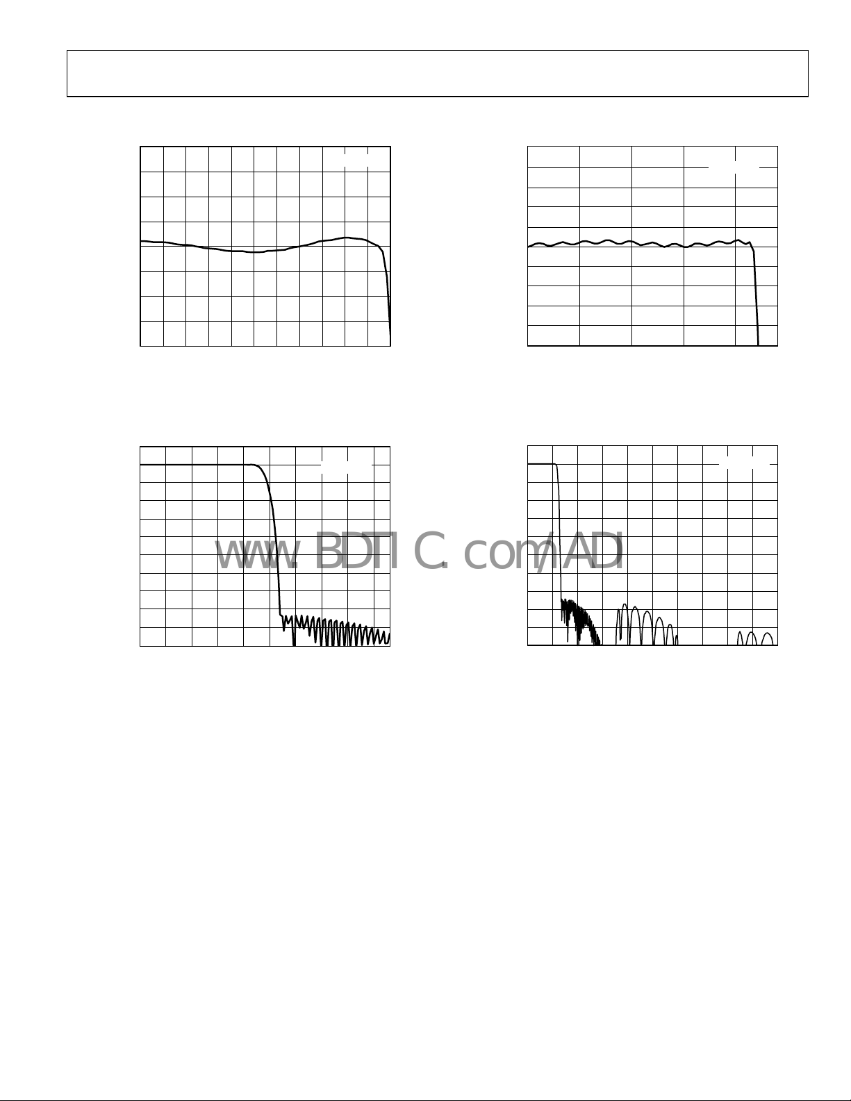
TYPICAL PERFORMANCE CHARACTERISTICS
0.20
0.15
0.10
0.05
0
GAIN (dB)
–0.05
–0.10
–0.15
–0.20
0 2 4 6 8 10121416182022
FREQUENCY (kHz)
Figure 8. ADC Pass-Band Filter Response
f
= 48kHz
S
06752-008
0.10
0.08
0.06
0.04
0.02
0
GAIN (dB)
–0.02
–0.04
–0.06
–0.08
–0.10
0 5 10 15 20
FREQUENCY (kHz)
Figure 10. DAC Pass-Band Filter Response
f
= 48kHz
S
06752-010
10
0
–10
–20
–30
–40
–50
GAIN (dB)
–60
–70
–80
–90
–100
0 2530354020151054
FREQUENCY (kHz)
f
= 48kHz
S
06752-009
5
Figure 9. ADC Stop-Band Filter Response
10
0
–10
–20
–30
–40
–50
GAIN (dB)
–60
–70
–80
–90
–100
02468101214161820
FREQUENCY (kHz)
f
Figure 11. DAC Stop-Band Filter Response
= 48kHz
S
06752-011
Rev. A | Page 15 of 52
ADAU1401
www.BDTIC.com/ADI
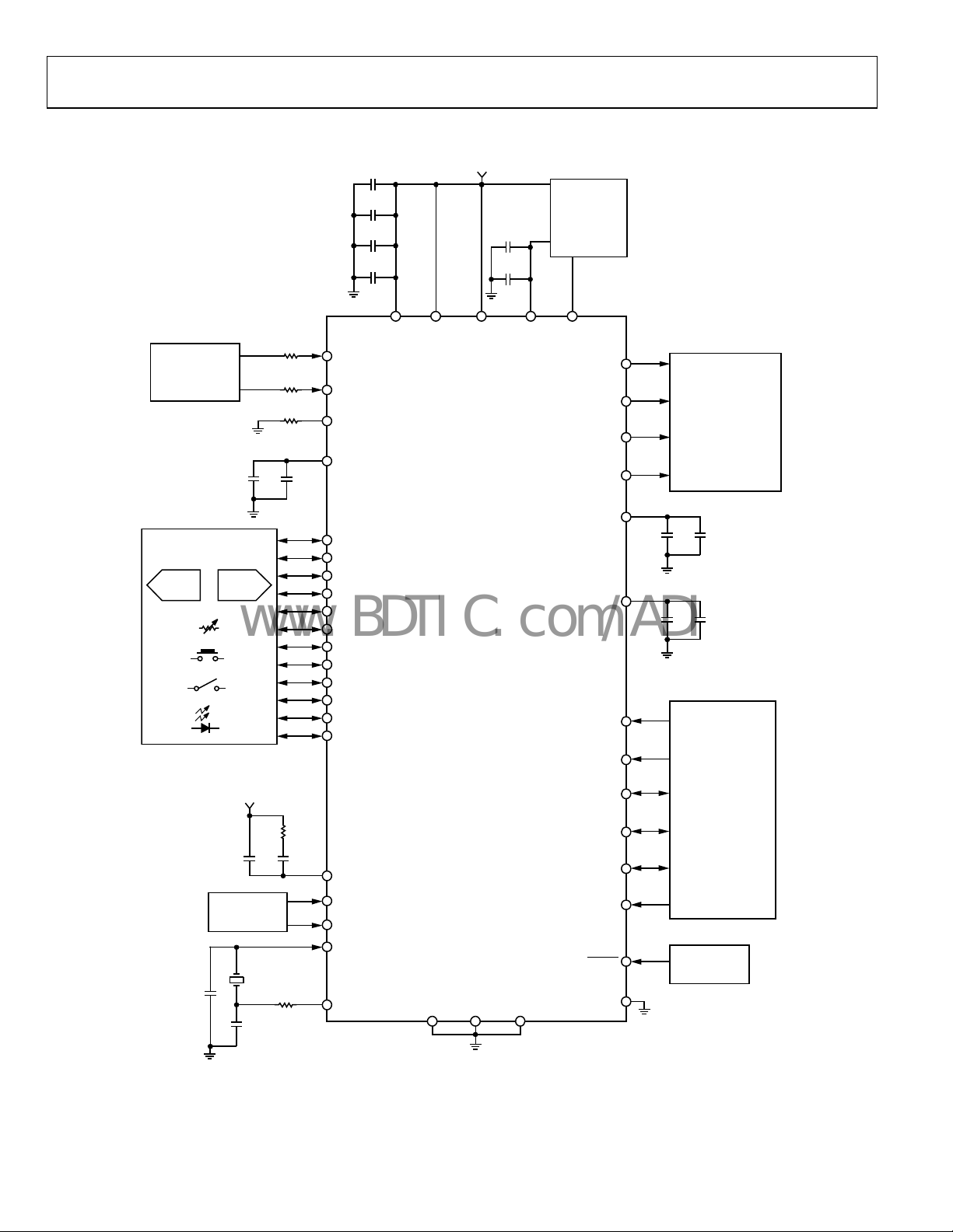
SYSTEM BLOCK DIAGRAM
100nF
3.3V
AUDIO ADC
INPUT SIGNALS
10µF
MULTIPURPOSE
PIN INTERF ACES
ADCs DACs
100nF
100nF
10µF
+
IOVDD PVDD AVDD DVDD VDRIVE
18k
18k
18k
+
100nF
ADC0
ADC1
ADC_RES
FILTA
MP0
MP1
MP2
MP3
MP4
MP5
MP6
MP7
MP8
MP9
MP10
MP11
ADAU1401
100nF
10µF
+
3.3V TO 1. 8V
REGULATOR
CIRCUIT
VOUT0
VOUT1
VOUT2
VOUT3
FILTD
CM
ADDR0
ADDR1/CDATA/WB
DAC OUTPUT FILTERS
(ACTIVE OR PASSIVE)
+
+
10µF
100nF10µF
100nF
3.3V
475
56nF3. 3nF
PLL_LF
PLL_MODE0
PLL_MODE1
MCLKI
OSCO
AGND DGND PG ND
22pF
PLL
SETTINGS
3MHz TO 25MHz
22pF
100
Figure 12. System Block Diagram
Rev. A | Page 16 of 52
CLATCH/WP
SDA/COUT
SCL/CCLK
SELFBOOT
RESET
RSVD
EEPROM,
MICROCONTRO LLER,
AND/OR SELF BOOT
LOGIC
RESET LOGIC
06752-012
 Loading...