Low Noise Stereo Codec with Enhanced
FEATURES
24-bit stereo audio ADC and DAC
400 mW speaker amplifier (into 8 Ω load)
Built-in sound engine for audio processing
Wind noise detection and autofiltering
Enhanced stereo capture (ESC)
Dual-band automatic level control (ALC)
6-band equalizer, including notch filter
Sampling rates from 8 kHz to 96 kHz
Stereo pseudo differential microphone input
Optional stereo digital microphone input pulse-density
modulation (PDM)
Stereo line output
PLL supporting a range of input clock rates
Analog and digital I/O 1.8 V to 3.3 V
Software control via SigmaStudio graphical user interface
Software-controllable, clickless mute
Software register and hardware pin standby mode
32-lead, 5 mm × 5 mm LFCSP or 30-ball, 6 × 5 bump WLCSP
APPLICATIONS
Digital still cameras
Digital video cameras
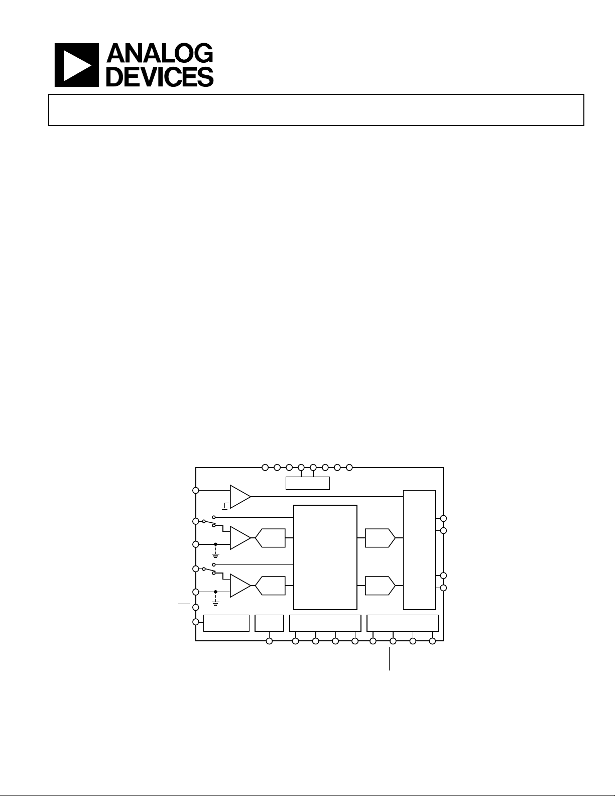
FUNCTIONAL BLOCK DIAGRAM
Recording and Playback Processing
ADAU1381
GENERAL DESCRIPTION
The ADAU1381 is a low power, 24-bit stereo audio codec. The
low noise DAC and ADC support sample rates from 8 kHz to
96 kHz. Low current draw and power saving modes make the
ADAU1381 ideal for battery-powered audio applications.
A configurable sound engine provides enhanced record and
playback processing to improve overall audio quality.
The record path includes two digital stereo microphone inputs
and an analog stereo input path. The analog inputs can be
configured for either a pseudo differential or a single-ended
stereo source. A dedicated analog beep input signal can be
mixed into any output path. The ADAU1381 includes a stereo
line output and speaker driver, which makes the device capable of
supporting dynamic speakers.
The serial control bus supports the I
the serial audio bus is programmable for I
justified, or TDM mode. A programmable PLL supports flexible
clock generation for all standard rates and available master clocks
from 11 MHz to 20 MHz.
2
C® or SPI protocols, and
2
S, left-justified, right-
CM
IOVDD
DGND
BEEP
LMIC/LMICN/
MICD1
LMICP
RMIC/RMICN/
MICD2
RMICP
PDN
MICBIAS
Rev. B
Information furnished by Analog Devices is believed to be accurate and reliable. However, no
responsibility is assumed by Analog Devices for its use, nor for any infringements of patents or other
rights of third parties that may result from its use. Specifications subject to change without notice. No
license is granted by implication or otherwise under any patent or patent rights of Analog Devices.
Trademarks and registered trademarks are the property of their respective owners.
PGA
PGA
PGA
MICROPHONE
BIAS
REGULATOR
LEFT
ADC
RIGHT
ADC
PLL
INPUT/OUTPUT PORTS
MCKI
ADC_SDATA/
DVDDOUT
AVDD1
AGND1
AVDD2
SOUND ENGINE
DECIMATION
FILTERS
WIND NOIS E
NOTCH FILTER
EQUALIZER
DIGITAL VOLUME
CONTROL
AUTOMATIC LEVEL
CONTROL
SERIAL DATA
GPIO1
BCLK/GPIO2
LRCLK/GPIO3
Figure 1.
One Technology Way, P.O. Box 9106, Norwood, MA 02062-9106, U.S.A.
Tel: 781.329.4700 www.analog.com
Fax: 781.461.3113 ©2009–2011 Analog Devices, Inc. All rights reserved.
AGND2
GPIO0
DAC_SDATA/
ADAU1381
LEFT
DAC
RIGHT
DAC
I2C/SPI
CONTROL P ORT
ADDR0/CDATA
ADDR1/CLATCH
OUTPUT
MIXER
SCL/CCLK
AOUTL
AOUTR
SPP
SPN
SDA/COUT
08313-001

ADAU1381
TABLE OF CONTENTS
Features.............................................................................................. 1
Input Signal Path ........................................................................ 30
Applications....................................................................................... 1
General Description ......................................................................... 1
Functional Block Diagram .............................................................. 1
Revision History ............................................................................... 3
Specifications..................................................................................... 4
Record Side Performance Specifications................................... 4
Output Side Performance Specifications................................... 6
Power Supply Specifications........................................................ 8
Typical Power Management Measurements ............................. 9
Digital Filters................................................................................. 9
Digital Input/Output Specifications......................................... 10
Digital Timing Specifications ...................................................11
Absolute Maximum Ratings.......................................................... 14
Thermal Resistance .................................................................... 14
ESD Caution................................................................................ 14
Analog-to-Digital Converters................................................... 31
Digital Dual-Band Automatic Level Control (ALC) ............. 31
Playback Signal Path ...................................................................... 32
Output Signal Paths ................................................................... 32
Digital-to-Analog Converters................................................... 32
Line Outputs ............................................................................... 32
Speaker Output........................................................................... 32
Control Ports................................................................................... 33
I2C Port ........................................................................................ 33
SPI Port........................................................................................ 36
Memory and Register Access.................................................... 36
Serial Data Input/Output Ports .................................................... 38
TDM Modes................................................................................ 38
General-Purpose Input/Outputs.................................................. 40
Sound Engine.................................................................................. 41
Pin Configuration and Function Descriptions........................... 15
Typical Performance Characteristics ........................................... 17
System Block Diagrams ................................................................. 20
Theory of Operation ...................................................................... 24
Startup, Initialization, and Power................................................. 25
Power-Up Sequence ................................................................... 25
Clock Generation and Management........................................ 26
Enabling Digital Power to Functional Subsystems................ 26
Setting Up the Sound Engine.................................................... 26
Power Reduction Modes............................................................ 26
Power-Down Sequence.............................................................. 26
Clocking and Sampling Rates .......................................................27
Core Clock................................................................................... 27
Sampling Rates............................................................................ 27
PLL ............................................................................................... 28
Signal Processing........................................................................ 41
Processing Flow.......................................................................... 41
Programming.............................................................................. 41
Parameter Memory .................................................................... 41
Applications Information.............................................................. 42
Power Supply Bypass Capacitors.............................................. 42
GSM Noise Filter........................................................................ 42
Grounding................................................................................... 42
Speaker Driver Supply Trace (AVDD2) .................................. 42
Exposed Pad PCB Design ......................................................... 42
Control Register Map..................................................................... 43
Clock Management, Internal Regulator, and PLL Control... 44
Record Path Configuration....................................................... 48
Serial Port Configuration.......................................................... 53
Audio Converter Configuration............................................... 58
Record Signal Path.......................................................................... 30
Rev. B | Page 2 of 84
Playback Path Configuration.................................................... 63

ADAU1381
Pad Configuration.......................................................................70
Outline Dimensions........................................................................84
Digital Subsystem Configuration..............................................77
REVISION HISTORY
1/11—Rev. A to Rev. B
PDN
Changes to Pin
Changes to Power-Down Pin (
Changes to Table 23 ........................................................................36
3/10—Rev. 0 to Rev. A
Changes to Output Side Performance Specifications Section
Condition Statement.....................................................................6
Added Endnote 1 to Table 3.............................................................8
Changes to Figure 23 ......................................................................20
Changes to Figure 24 ......................................................................21
Changes to Figure 25 ......................................................................22
Changes to Figure 26 ......................................................................23
Changes to Table 27 ........................................................................43
Added Register 16434 (0x4032), Dejitter Control Section ........76
Changes to Ordering Guide...........................................................84
10/09—Revision 0: Initial Version
Description in Table 10 .............................16
PDN
) Section..............................26
Ordering Guide...........................................................................84
Rev. B | Page 3 of 84

ADAU1381
SPECIFICATIONS
Performance of all channels is identical, exclusive of the interchannel gain mismatch and interchannel phase deviation specifications.
Supply voltages AVDD = AVDD1 = AVDD2 = I/O supply = 3.3 V, digital supply = 1.5 V, unless otherwise noted; temperature = 25°C;
master clock (MCLK) = 12.288 MHz (f
word width = 24 bits; load capacitance (digital output) = 20 pF; load current (digital output) = 2 mA; high level input voltage = 0.7 × IOVDD;
and low level input voltage = 0.3 × IOVDD. All power management registers are set to their default states.
RECORD SIDE PERFORMANCE SPECIFICATIONS
Specifications guaranteed at 25°C (ambient).
Table 1.
Parameter Test Conditions/Comments Min Typ Max Unit
ANALOG-TO-DIGITAL CONVERTERS
ADC Resolution All ADCs 24 Bits
Digital Attenuation Step 0.375 dB
Digital Attenuation Range 95 dB
INPUT RESISTANCE
Noninverting Inputs PGA
(LMICP, RMICP)
Inverting Inputs PGA (LMICN, RMICN) 0 dB gain 62 kΩ
6 dB gain 32 kΩ
10 dB gain 22 kΩ
14 dB gain 14 kΩ
17 dB gain 10 kΩ
20 dB gain 8 kΩ
26 dB gain 5 kΩ
32 dB gain 4 kΩ
Beep Input PGA 0 dB 20 kΩ
6 dB 9 kΩ
10 dB 6 kΩ
14 dB 3.5 kΩ
−23 dB 50 kΩ
20 dB 2 kΩ
26 dB 2 kΩ
32 dB 2 kΩ
SINGLE-ENDED MICROPHONE INPUT
TO ADC PATH
Full-Scale Input Voltage (0 dB) Scales linearly with AVDD AVDD/3.3 V rms
AVDD = 1.8 V 0.55 (1.56) V rms (V p-p)
AVDD = 3.3 V 1.0 (2.83) V rms (V p-p)
Dynamic Range −60 dB input
With A-Weighted Filter (RMS) AVDD = 1.8 V 96 dB
AVDD = 3.3 V 94 99.2 dB
No Filter (RMS) AVDD = 1.8 V 92 dB
AVDD = 3.3 V 92 96.5 dB
Total Harmonic Distortion + Noise −3 dBFS
AVDD = 1.8 V −88 dB
AVDD = 3.3 V −90 dB
Signal-to-Noise Ratio
With A-Weighted Filter (RMS) AVDD = 1.8 V 96 dB
AVDD = 3.3 V 100 dB
No Filter (RMS) AVDD = 1.8 V 92 dB
AVDD = 3.3 V 97 dB
= 48 kHz, 256 × fS mode); input sample rate = 48 kHz; measurement bandwidth = 20 Hz to 20 kHz;
S
All gain settings 500 kΩ
Rev. B | Page 4 of 84

ADAU1381
Parameter Test Conditions/Comments Min Typ Max Unit
Left/Right Microphone PGA Gain
Range
Left/Right Microphone PGA Mute
Attenuation
Interchannel Gain Mismatch AVDD = 3.3 V 50 mdB
Offset Error AVDD = 3.3 V 0.25 mV
Gain Error AVDD = 3.3 V −1 %
Interchannel Isolation AVDD = 3.3 V −98 dB
Power Supply Rejection Ratio CM capacitor = 10 F
AVDD = 3.3 V, 100 mV p-p at 217 Hz −55 dB
AVDD = 3.3 V, 100 mV p-p at 1 kHz −55 dB
DIFFERENTIAL MICROPHONE INPUT TO
ADC PATH
Full-Scale Input Voltage (0 dB) Scales linearly with AVDD AVDD/3.3 V rms
AVDD = 1.8 V 0.55 (1.56) V rms (V p-p)
AVDD = 3.3 V 1.0 (2.83) V rms (V p-p)
Dynamic Range −60 dB input
With A-Weighted Filter (RMS) AVDD = 1.8 V 96 dB
AVDD = 3.3 V 94 99.2 dB
No Filter (RMS) AVDD = 1.8 V 92 dB
AVDD = 3.3 V 92 96.5 dB
Total Harmonic Distortion + Noise −3 dBFS
AVDD = 1.8 V −84 dB
AVDD = 3.3 V −85 dB
Signal-to-Noise Ratio
With A-Weighted Filter (RMS) AVDD = 1.8 V 96 dB
AVDD = 3.3 V 100 dB
No Filter (RMS) AVDD = 1.8 V 92 dB
AVDD = 3.3 V 97 dB
Left/Right Microphone PGA Mute
Attenuation
Interchannel Gain Mismatch AVDD = 3.3 V 50 mdB
Offset Error AVDD = 3.3 V 0.25 mV
Gain Error AVDD = 3.3 V −1 %
Interchannel Isolation AVDD = 3.3 V −85 dB
Common-Mode Rejection Ratio AVDD = 3.3 V, 100 mV rms, 1 kHz −60 dB
AVDD = 3.3 V, 100 mV rms, 20 kHz −45 dB
BEEP TO LINE OUTPUT PATH
Full-Scale Input Voltage (0 dB) Scales linearly with AVDD AVDD/3.3 V rms
AVDD = 1.8 V 0.55 (1.56) V rms (V p-p)
AVDD = 3.3 V 1.0 (2.83) V rms (V p-p)
Total Harmonic Distortion + Noise
AVDD = 1.8 V −88 dB
AVDD = 3.3 V −88 dB
Signal-to-Noise Ratio
With A-Weighted Filter (RMS) AVDD = 1.8 V 99 dB
AVDD = 3.3 V 105 dB
No Filter (RMS) AVDD = 1.8 V 96 dB
AVDD = 3.3 V 102 dB
AVDD = 3.3 V 0 32 dB
AVDD = 3.3 V; mute set by Register
0x400E, Bit 1, and Register 0x400F, Bit 1
AVDD = 3.3 V; mute set by Register
0x400E, Bit 1, and Register 0x400F, Bit 1
−3 dBFS input, measured at AOUTL pin,
beep gain set to 0 dB
−98 dB
−98 dB
Rev. B | Page 5 of 84

ADAU1381
Parameter Test Conditions/Comments Min Typ Max Unit
Dynamic Range −60 dB input
With A-Weighted Filter (RMS) AVDD = 1.8 V 99 dB
AVDD = 3.3 V 105 dB
No Filter (RMS) AVDD = 1.8 V 96 dB
AVDD = 3.3 V 102 dB
Beep Input Mute Attenuation
Offset Error AVDD = 3.3 V 10 mV
Gain Error AVDD = 3.3 V −0.3 dB
Interchannel Gain Mismatch 30 mdB
Beep Input PGA Gain Range AVDD = 3.3 V −23 +32 dB
Beep Playback Mixer Gain Range AVDD = 3.3 V −15 +6 dB
Power Supply Rejection Ratio CM capacitor = 10 F
AVDD = 3.3 V, 100 mV p-p at 217 Hz −58 dB
AVDD = 3.3 V, 100 mV p-p at 1 kHz −72 dB
MICROPHONE BIAS Microphone bias enabled
Bias Voltage
0.65 × AVDD AVDD = 1.8 V, low bias 1.17 V
AVDD = 3.3 V, low bias 2.145 V
0.90 × AVDD AVDD = 1.8 V, high bias 1.62 V
AVDD = 3.3 V, high bias 2.97 V
Bias Current Source
Noise in the Signal Bandwidth AVDD = 3.3 V, 20 Hz to 20 kHz
High bias, high performance 39 nV√Hz
High bias, low performance 78 nV√Hz
Low bias, high performance 25 nV√Hz
Low bias, low performance 35 nV√Hz
AVDD = 1.8 V, 20 Hz to 20 kHz
High bias, high performance 35 nV√Hz
High bias, low performance 45 nV√Hz
Low bias, high performance 23 nV√Hz
Low bias, low performance 23 nV√Hz
AVDD = 3.3 V; mute set by
Register 0x4008, Bit 3
AVDD = 3.3 V, high bias, high
performance
−90 dB
5 mA
OUTPUT SIDE PERFORMANCE SPECIFICATIONS
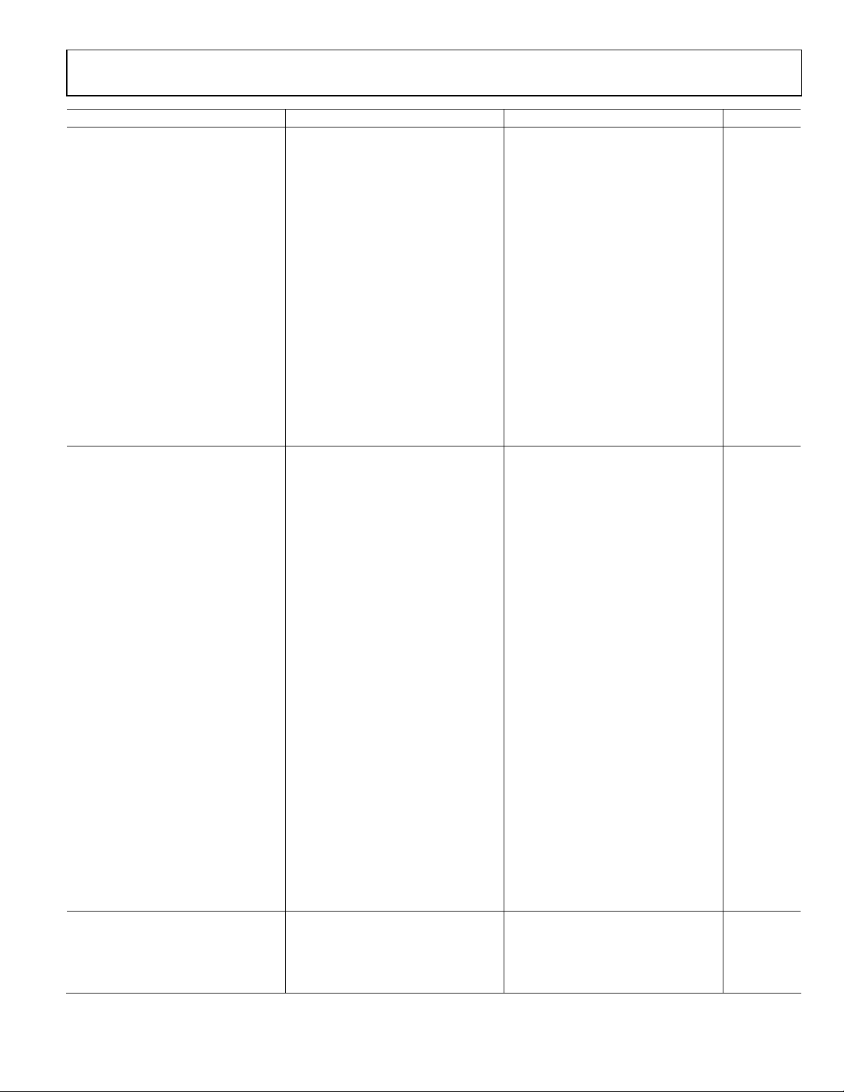
Specifications guaranteed at 25°C (ambient). The output load for the speaker output path is an 8 Ω, 400 mW speaker.
Table 2.
Parameter Test Conditions/Comments Min Typ Max Unit
DIGITAL-TO-ANALOG CONVERTERS
DAC Resolution All DACs 24 Bits
Digital Attenuation Step 0.375 dB
Digital Attenuation Range 95 dB
DAC TO LINE OUTPUT PATH
Full-Scale Output Voltage (0 dB) Scales linearly with AVDD AVDD/3.3 V rms
AVDD = 1.8 V 0.55 (1.56) V rms (V p-p)
AVDD = 3.3 V 1.0 (2.83) V rms (V p-p)
Line Output Mute Attenuation,
DAC to Mixer Path Muted
Line Output Mute Attenuation,
Line Output Muted
AVDD = 3.3 V; mute set by Register
0x401C, Bit 5, and Register 0x401E, Bit 6
AVDD = 3.3 V; mute set by Register
0x4025, Bit 1, and Register 0x4026, Bit 1
Rev. B | Page 6 of 84
−85 dB
−85 dB
ADAU1381
Parameter Test Conditions/Comments Min Typ Max Unit
Dynamic Range −60 dB input
With A-Weighted Filter (RMS) AVDD = 1.8 V 99 dB
AVDD = 3.3 V 94 103 dB
No Filter (RMS) AVDD = 1.8 V 97 dB
AVDD = 3.3 V 92 100 dB
Total Harmonic Distortion + Noise −3 dBFS dB
AVDD = 1.8 V −88 dB
AVDD = 3.3 V −88 dB
Signal-to-Noise Ratio
With A-Weighted Filter (RMS) AVDD = 1.8 V 99 dB
AVDD = 3.3 V 103 dB
No Filter (RMS) AVDD = 1.8 V 97 dB
AVDD = 3.3 V 100 dB
Power Supply Rejection Ratio CM capacitor = 10 F
AVDD = 3.3 V, 100 mV p-p at 217 Hz −55 dB
AVDD = 3.3 V, 100 mV p-p at 1 kHz −63 dB
Gain Error AVDD = 3.3 V −1 dB
Interchannel Gain Mismatch AVDD = 3.3 V 50 mdB
Offset Error AVDD = 3.3 V 10 mV
DAC TO SPEAKER OUTPUT PATH PO = output power
Differential Full-Scale Output Voltage
(0 dB)
AVDD = 1.8 V 1.1 (3.12) V rms (V p-p)
AVDD = 3.3 V 2.0 (5.66) V rms (V p-p)
Total Harmonic Distortion + Noise
4 Ω Load AVDD = 1.8 V, PO = 50 mW −60 dB
AVDD = 3.3 V, PO = 175 mW −60 dB
8 Ω Load AVDD = 1.8 V, PO = 50 mW −60 dB
AVDD = 3.3 V, PO = 175 mW −60 dB
AVDD = 3.3 V, PO = 330 mW −60 dB
AVDD = 3.3 V, PO = 440 mW −16 dB
Dynamic Range −60 dB input
With A-Weighted Filter (RMS) AVDD = 1.8 V 100 dB
AVDD = 3.3 V 94 105 dB
No Filter (RMS) AVDD = 1.8 V 98 dB
AVDD = 3.3 V 92 103 dB
Signal-to-Noise Ratio
With A-Weighted Filter (RMS) AVDD = 1.8 V 100 dB
AVDD = 3.3 V 105 dB
No Filter (RMS) AVDD = 1.8 V 98 dB
AVDD = 3.3 V 103 dB
Power Supply Rejection Ratio CM capacitor = 10 F
AVDD = 3.3 V,100 mV p-p at 217 Hz −55 dB
AVDD = 3.3 V, 100 mV p-p at 1 kHz −55 dB
Differential Offset Error AVDD = 3.3 V 2 mV
Mono Mixer Mute Attenuation,
DAC to Mixer Path Muted
BEEP TO SPEAKER OUTPUT PATH PO = output power
Differential Full-Scale Output Voltage
(0 dB)
AVDD = 1.8 V 1.1 (3.12) V rms (V p-p)
AVDD = 3.3 V 2.0 (5.66) V rms (V p-p)
Scales linearly with AVDD AVDD/1.65 V rms
Mute set by Register 0x401F, Bit 0 −90 dB
Scales linearly with AVDD AVDD/1.65 V rms
Rev. B | Page 7 of 84
ADAU1381
Parameter Test Conditions/Comments Min Typ Max Unit
Total Harmonic Distortion + Noise
8 Ω, 1 nF load, AVDD = 1.8 V, PO = 50 mW −60 dB
AVDD = 3.3 V, PO = 175 mW −60 dB
Dynamic Range −60 dB input
With A-Weighted Filter (RMS) AVDD = 1.8 V 97 dB
AVDD = 3.3 V 103 dB
No Filter (RMS) AVDD = 1.8 V 94 dB
AVDD = 3.3 V 100 dB
Signal-to-Noise Ratio
With A-Weighted Filter (RMS) AVDD = 1.8 V 98 dB
AVDD = 3.3 V 103 dB
No Filter (RMS) AVDD = 1.8 V 96 dB
AVDD = 3.3 V 101 dB
Power Supply Rejection Ratio CM capacitor = 10 F
100 mV p-p at 217 Hz −57 dB
100 mV p-p at 1 kHz −60 dB
Differential Offset Error 2 mV
Mono Mixer Mute Attenuation,
Beep to Mixer Path Muted
REFERENCE (CM PIN)
Common-Mode Reference Output AVDD/2 V
Mute set by Register 0x401F, Bit 0 −90 dB
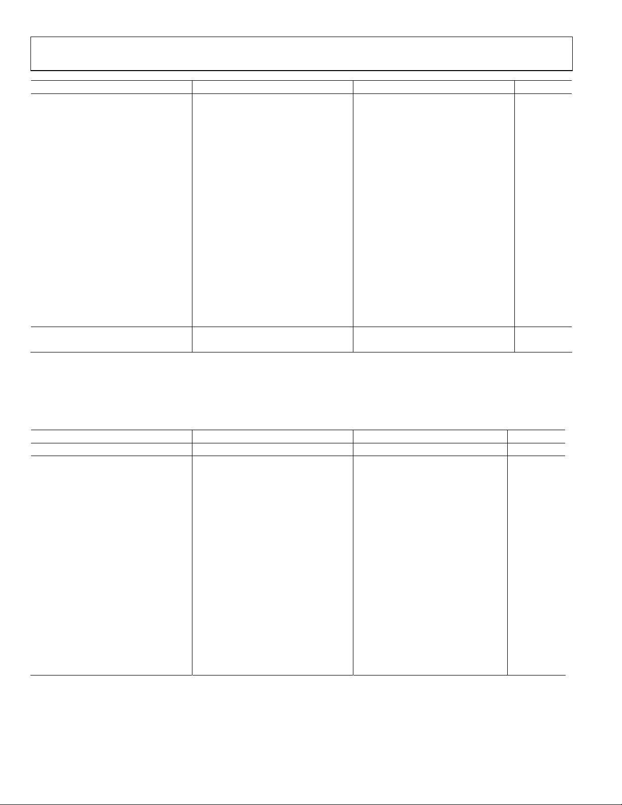
POWER SUPPLY SPECIFICATIONS
AVDD1 and AVDD2 must always be equal. Power supply measurements are taken with the sound engine processing path enabled.
Table 3.
Parameter Test Conditions/Comments Min Typ Max Unit
AVDD1, AVDD2 1.81 3.3 3.65 V
IOVDD 1.63 3.3 3.65 V
Digital I/O Current (IOVDD = 3.3 V) 20 pF capacitive load on all digital pins
= 48 kHz 0.20 mA
Slave Mode, Analog I/O,
12.288 MHz External MCLK Input
f
f
Master Mode, MCKO Disabled fS = 48 kHz 1.25 mA
f
f
Digital I/O Current (IOVDD = 1.8 V) 20 pF capacitive load on all digital pins
Slave Mode, Analog I/O,
12.288 MHz External MCLK Input
f
f
Master Mode, MCKO Disabled fS = 48 kHz 0.68 mA
f
f
Analog Current (AVDD) See Table 4
1
The zero-cross detection of the beep path is not supported at AVDD1, AVDD2 < 2.2 V.
f
S
= 96 kHz 0.35 mA
S
= 8 kHz 0.04 mA
S
= 96 kHz 2.50 mA
S
= 8 kHz 0.22 mA
S
= 48 kHz 0.10 mA
f
S
= 96 kHz 0.18 mA
S
= 8 kHz 0.02 mA
S
= 96 kHz 1.33 mA
S
= 8 kHz 0.12 mA
S
Rev. B | Page 8 of 84

ADAU1381
TYPICAL POWER MANAGEMENT MEASUREMENTS
Master clock = 12.288 MHz, PLL is active in integer mode at a 256 × fS input rate for fS = 48 kHz, analog and digital input tones are
−1 dBFS with a frequency of 1 kHz. Analog input and output are simultaneously active. Pseudo differential stereo input is routed to
ADCs, and DACs are routed to stereo line output with a 16 k load. ADC input at −1 dBFS, DAC input at 0 dBFS. The speaker output is
disabled. The serial port is configured in slave mode. The beep path is disabled. The sound engine processing path is enabled. Current
measurements are given in units of mA rms.
Table 4. Mixer Boost and Power Management Conditions
Typical AVDD Current
Operating Voltage Power Management Mode1 Mixer Boost Mode2
AVDD = IOVDD = 3.3 V Normal (default) Normal operation 16.84 88.5 93.0
Boost Level 1 16.88 88.5 93.0
Boost Level 2 16.92 88.5 93.0
Boost Level 3 17.00 88.5 93.0
Extreme power saving Normal operation 15.66 88.0 87.5
Boost Level 1 15.68 88.0 87.5
Boost Level 2 15.70 88.0 87.5
Boost Level 3 15.75 88.0 87.5
Enhanced performance Normal operation 17.43 88.5 94.5
Boost Level 1 17.50 88.5 94.5
Boost Level 2 17.53 88.5 94.5
Boost Level 3 17.63 88.5 94.5
Power saving Normal operation 16.25 89.0 90.5
Boost Level 1 16.28 89.0 90.5
Boost Level 2 16.31 89.0 90.5
Boost Level 3 16.38 89.0 90.5
AVDD = IOVDD = 1.8 V Normal (default) Normal operation 15.15 88.5 89.5
Boost Level 1 15.19 88.5 89.5
Boost Level 2 15.23 88.5 89.5
Boost Level 3 15.30 88.5 89.5
Extreme power saving Normal operation 14.03 86.5 85.5
Boost Level 1 14.05 86.5 85.5
Boost Level 2 14.07 86.5 85.5
Boost Level 3 14.12 86.5 85.5
Enhanced performance Normal operation 15.71 88.5 90.5
Boost Level 1 15.76 88.5 90.5
Boost Level 2 15.81 88.5 90.5
Boost Level 3 15.89 88.5 90.5
Power saving Normal operation 14.59 88.0 88.0
Boost Level 1 14.62 88.0 88.0
Boost Level 2 14.65 88.0 88.0
Boost Level 3 14.71 88.0 88.0
1
Set by Register 0x4009, Bits[4:1], and Register 0x4029, Bits[5:2].
2
Set by Register 0x4009, Bits[6:5].
Consumption (mA)
Typical ADC
THD + N (dB)
Typical Line Output
THD + N (dB)
DIGITAL FILTERS
Table 5.
Parameter Mode Factor Min Typ Max Unit
ADC DECIMATION FILTER
Pass Band 0.4375 × f
Pass-Band Ripple ±0.015 dB
Transition Band 0.5 × f
Stop Band 0.5625 × f
Stop-Band Attenuation 70 dB
Group Delay 22.9844/f
All modes, typ value is for 48 kHz
Rev. B | Page 9 of 84
S
S
S
S
21 kHz
24 kHz
27 kHz
479 µs

ADAU1381
Parameter Mode Factor Min Typ Max Unit
DAC INTERPOLATION FILTER
Pass Band 48 kHz mode, typ value is for 48 kHz 0.4535 × f
96 kHz mode, typ value is for 96 kHz 0.3646 × f
Pass-Band Ripple 48 kHz mode, typ value is for 48 kHz ±0.01 dB
96 kHz mode, typ value is for 96 kHz ±0.05 dB
Transition Band 48 kHz mode, typ value is for 48 kHz 0.5 × f
96 kHz mode, typ value is for 96 kHz 0.5 × f
S
S
Stop Band 48 kHz mode, typ value is for 48 kHz 0.5465 × f
96 kHz mode, typ value is for 96 kHz 0.6354 × f
Stop-Band Attenuation 48 kHz mode, typ value is for 48 kHz 70 dB
96 kHz mode, typ value is for 96 kHz 70 dB
Group Delay 48 kHz mode, typ value is for 48 kHz 25/f
96 kHz mode, typ value is for 96 kHz 11/f
S
S
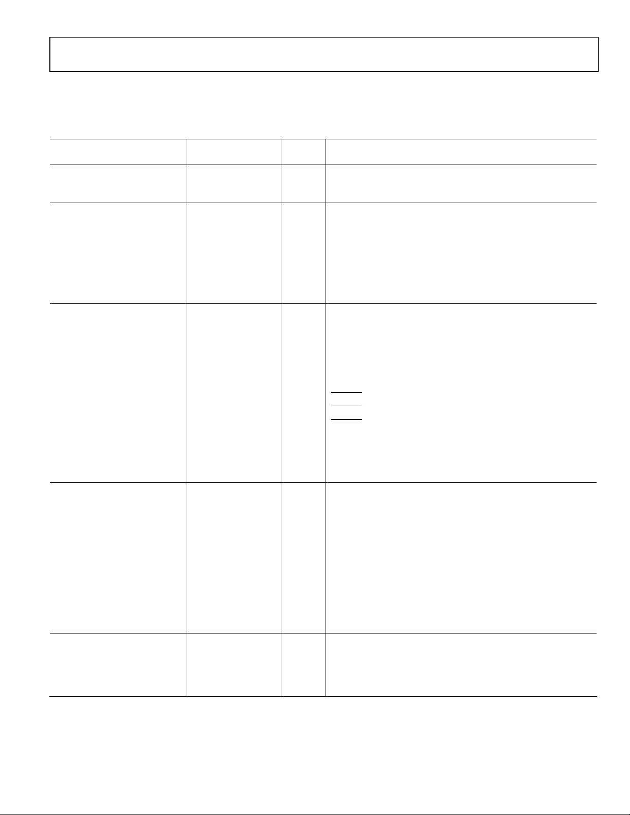
DIGITAL INPUT/OUTPUT SPECIFICATIONS
−25°C < TA < +85°C, IOVDD = 1.62 V to 3.63 V, unless otherwise specified.
Table 6.
Parameter Conditions/Comments Min Typ Max Unit
HIGH LEVEL INPUT VOLTAGE (VIH) 0.7 × IOVDD V
LOW LEVEL INPUT VOLTAGE (VIL) IOVDD ≥ 2.97 V 0.3 × IOVDD V
1.8 V ≤ IOVDD ≤ 2.97 V 0.2 × IOVDD V
IOVDD < 1.8 V 0.1 × IOVDD V
INPUT LEAKAGE IIH at VIH = 2.4 V ±0.17 µA
I
I
I
I
I
I
HIGH LEVEL OUTPUT VOLTAGE (VOH)
LOW LEVEL OUTPUT VOLTAGE (VOL)
INPUT CAPACITANCE 5 pF
at VIL = 0.8 V ±0.17 µA
IL
of MCKI −7 µA
IL
with internal pull-up ±0.7 µA
IH
with internal pull-down −7 µA
IL
with internal pull-up 5 µA
IH
with internal pull-down ±0.18 µA
IL
For low drive strength, I
at IOVDD = 3.3 V, I
IOVDD = 1.8 V; for high drive strength, I
and I
= 3 mA at IOVDD = 3.3 V, IOH = 0.9 mA and
OL
= 0.9 mA at IOVDD = 1.8 V
I
OL
For low drive strength, I
at IOVDD = 3.3 V, I
IOVDD = 1.8 V; for high drive strength, I
and I
= 3 mA at IOVDD = 3.3 V, IOH = 0.9 mA and
OL
= 0.9 mA at IOVDD = 1.8 V
I
OL
= 2 mA and IOL = 2 mA
OH
= 0.6 mA and IOL = 0.6 mA at
OH
= 2 mA and IOL = 2 mA
OH
= 0.6 mA and IOL = 0.6 mA at
OH
= 3 mA
OH
= 3 mA
OH
22 kHz
S
35 69 kHz
S
24 kHz
48 kHz
26 kHz
S
61 kHz
S
521 µs
115 µs
IOVDD − 0.4 V
0.4 V
Rev. B | Page 10 of 84
ADAU1381
DIGITAL TIMING SPECIFICATIONS
−25°C < TA < +85°C, IOVDD = 1.62 V to 3.63 V, unless otherwise specified.
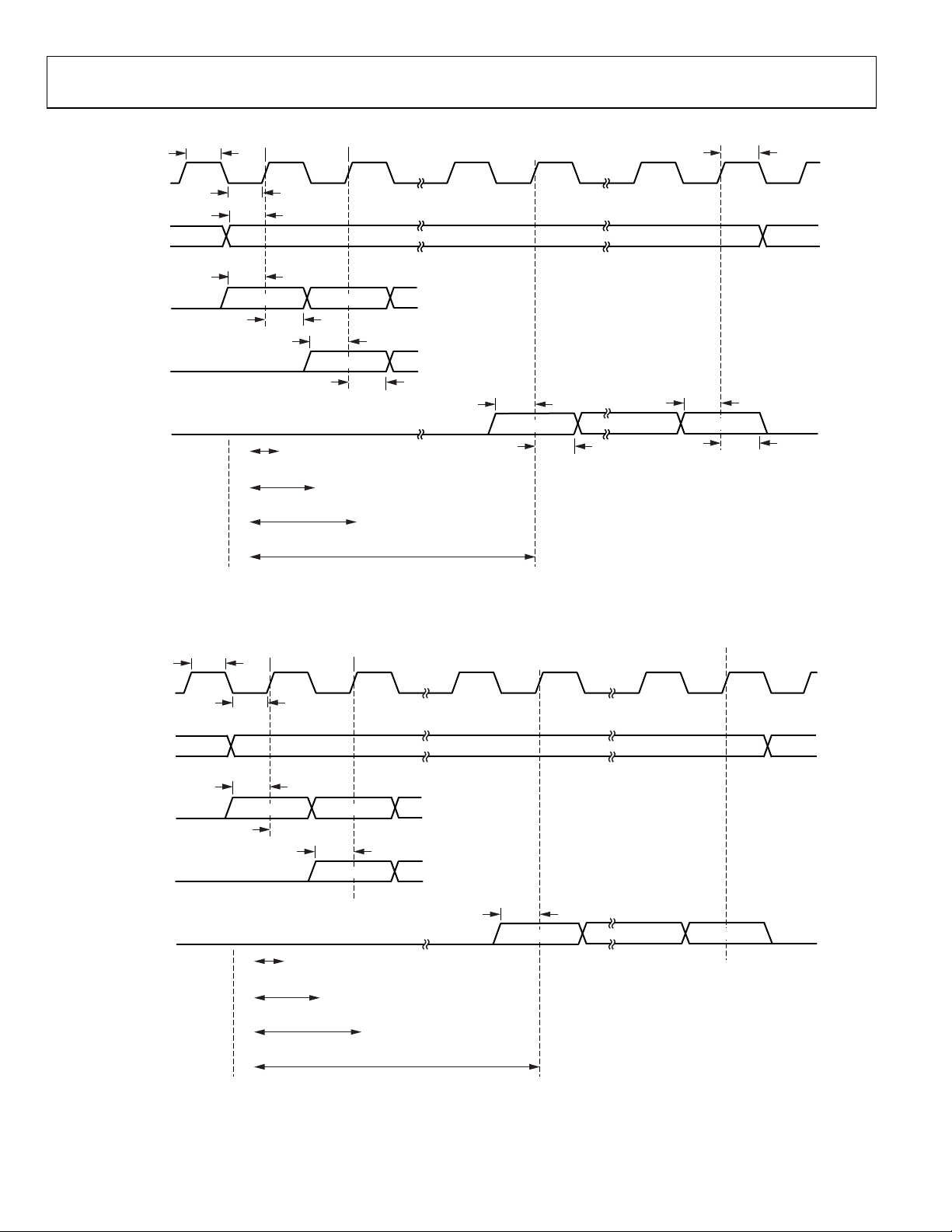
Table 7. Digital Timing
Limit
Parameter t
MASTER CLOCK
tMP 50 90.9 ns Master clock (MCLK) period (that is, period of the signal input to MCKI).
Duty Cycle 30 70 %
SERIAL PORT
t
10 ns BCLK pulse width low.
BIL
t
10 ns BCLK pulse width high.
BIH
t
5 ns LRCLK setup. Time to BCLK rising.
LIS
t
5 ns LRCLK hold. Time from BCLK rising.
LIH
t
5 ns DAC_SDATA setup. Time to BCLK rising.
SIS
t
5 ns DAC_SDATA hold. Time from BCLK rising.
SIH
t
70 ns ADC_SDATA delay. Time from BCLK falling in master mode.
SODM
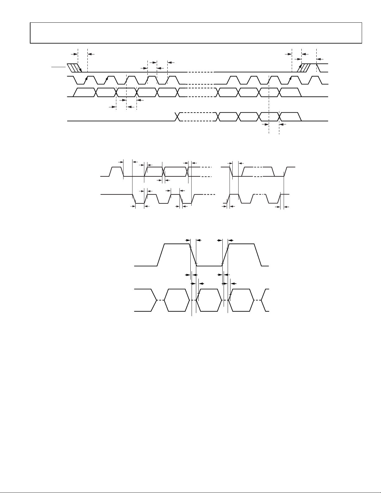
SPI PORT
f
5 MHz CCLK frequency, read operation, IOVDD = 1.8 V ± 10%.
CCLK,R
f
10 MHz CCLK frequency, read operation, IOVDD = 3.3 V ± 10%.
CCLK,R
f
25 MHz CCLK frequency, write operation, IOVDD = 1.8 V ± 10%.
CCLK,W
f
25 MHz CCLK frequency, write operation, IOVDD = 3.3 V ± 10%.
CCLK,W
t
10 ns CCLK pulse width low.
CCPL
t
10 ns CCLK pulse width high.
CCPH
t
10 ns
CLS
t
5 ns
CLH
t
10 ns
CLPH
t
5 ns CDATA setup. Time to CCLK rising.
CDS
t
5 ns CDATA hold. Time from CCLK rising.
CDH
t
70 COUT delay from CCLK edge to valid data, IOVDD = 1.8 V ± 10%.
COD
40 ns COUT delay from CCLK edge to valid data, IOVDD = 3.3 V ± 10%.
I2C PORT
f
400 kHz SCL frequency.
SCL
t
0.6 µs SCL high.
SCLH
t
1.3 µs SCL low.
SCLL
t
0.6 µs Setup time; relevant for repeated start condition.
SCS
t
0.6 µs Hold time. After this period, the first clock is generated.
SCH
tDS 100 ns Data setup time.
t
300 ns SCL rise time.
SCR
t
300 ns SCL fall time.
SCF
t
300 ns SDA rise time.
SDR
t
300 ns SDA fall time.
SDF
t
0.6 µs Bus-free time. Time between stop and start.
BFT
DIGITAL MICROPHONE RL = 1 MΩ, CL = 14 pF.
t
10 ns Digital microphone clock fall time.
DCF
t
10 ns Digital microphone clock rise time.
DCR
t
22 30 ns Digital microphone delay time for valid data.
DDV
t
0 12 ns Digital microphone delay time for data three-stated.
DDH
t
MIN
MAX
Unit Description
setup. Time to CCLK rising.
CLATCH
hold. Time from CCLK rising.
CLATCH
pulse width high.
CLATCH
Rev. B | Page 11 of 84
ADAU1381
Digital Timing Diagrams
t
LIH
t
SIS
LSB
t
SIH
08313-002
BCLK
LRCLK
DAC_SDATA
LEFT-JUSTIFIED
RIGHT-JUSTIFIED
MODE
DAC_SDATA
2
I
S MODE
DAC_SDATA
MODE
t
BIH
t
BIL
t
LIS
t
SIS
MSB
t
SIH
8-BIT CLOCKS
(24-BIT DATA)
12-BIT CLO CKS
(20-BIT DATA)
14-BIT CLO CKS
(18-BIT DATA)
16-BIT CLO CKS
(16-BIT DATA)
MSB – 1
t
SIS
MSB
t
SIH
t
SIS
MSB
t
SIH
Figure 2. Serial Input Port Timing
BCLK
LRCLK
ADC_SDATA
LEFT-JUSTIFIED
MODE
ADC_SDATA
2
I
S MODE
ADC_SDATA
RIGHT-JUSTIFIED
MODE
t
BIH
t
BIL
t
SODM
MSB
8-BIT CLO CKS
(24-BIT DAT A)
12-BIT CLOCKS
(20-BIT DAT A)
14-BIT CLOCKS
(18-BIT DAT A)
16-BIT CLOCKS
(16-BIT DAT A)
t
SODM
MSB – 1
MSB
t
SODM
MSB
LSB
08313-003
Figure 3. Serial Output Port Timing
Rev. B | Page 12 of 84
ADAU1381
t
CLS
t
CCPL
CLATCH
CCLK
CDATA
COUT
t
CCPH
t
t
CDS
CDH
Figure 4. SPI Port Timing
t
t
SDR
SCR
t
DS
t
SDF
t
SCLL
t
SCLH
t
SCF
Figure 5. I
2
C Port Timing
t
SCS
t
SCH
SDA
SCL
t
SCH
t
CLH
t
COD
t
BFT
08313-005
t
CLPH
08313-004
t
CLK
DATA1/
DATA1 DATA1 DATA2DATA2
DATA2
DCF
t
DDH
t
DDV
t
DDH
Figure 6. Digital Microphone Timing
t
DCR
t
DDV
08313-106
Rev. B | Page 13 of 84
ADAU1381
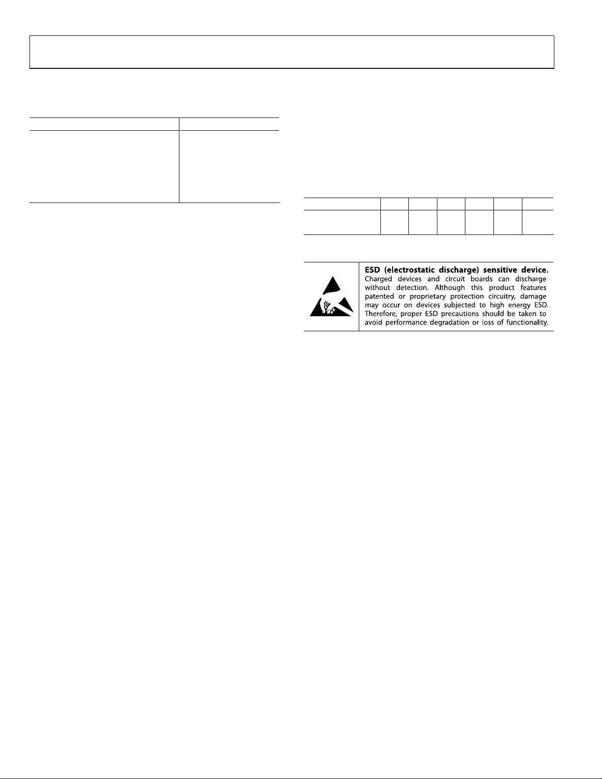
ABSOLUTE MAXIMUM RATINGS
Table 8.
Parameter Rating
Power Supply (AVDD1 = AVDD2) −0.3 V to +3.9 V
Input Current (Except Supply Pins) ±20 mA
Analog Input Voltage (Signal Pins) –0.3 V to VDD + 0.3 V
Digital Input Voltage (Signal Pins) −0.3 V to VDD + 0.3 V
Operating Temperature Range (Case) −25°C to +85°C
Storage Temperature Range −65°C to +150°C
Stresses above those listed under Absolute Maximum Ratings
may cause permanent damage to the device. This is a stress
rating only; functional operation of the device at these or any
other conditions above those indicated in the operational
section of this specification is not implied. Exposure to absolute
maximum rating conditions for extended periods may affect
device reliability.
THERMAL RESISTANCE
In Ta b le 9 , θJA is the junction-to-ambient thermal resistance, θJB is
the junction-to-board thermal resistance, θ
thermal resistance, ψ
mal resistance, and ψ
is the in-use junction-to-top of package ther-
JB
is the in-use junction-to-board thermal
JT
is the junction-to-case
JC
resistance. All characteristics are for a 4-layer board.
Table 9. Thermal Resistance
Package Type θ
32-Lead LFCSP 35 19 2.5 18 0.3 °C/W
30-Ball WLCSP 39 7 0.5 °C/W
JA
θJB θ
JC
ψJB ψJT Unit
ESD CAUTION
Rev. B | Page 14 of 84
ADAU1381
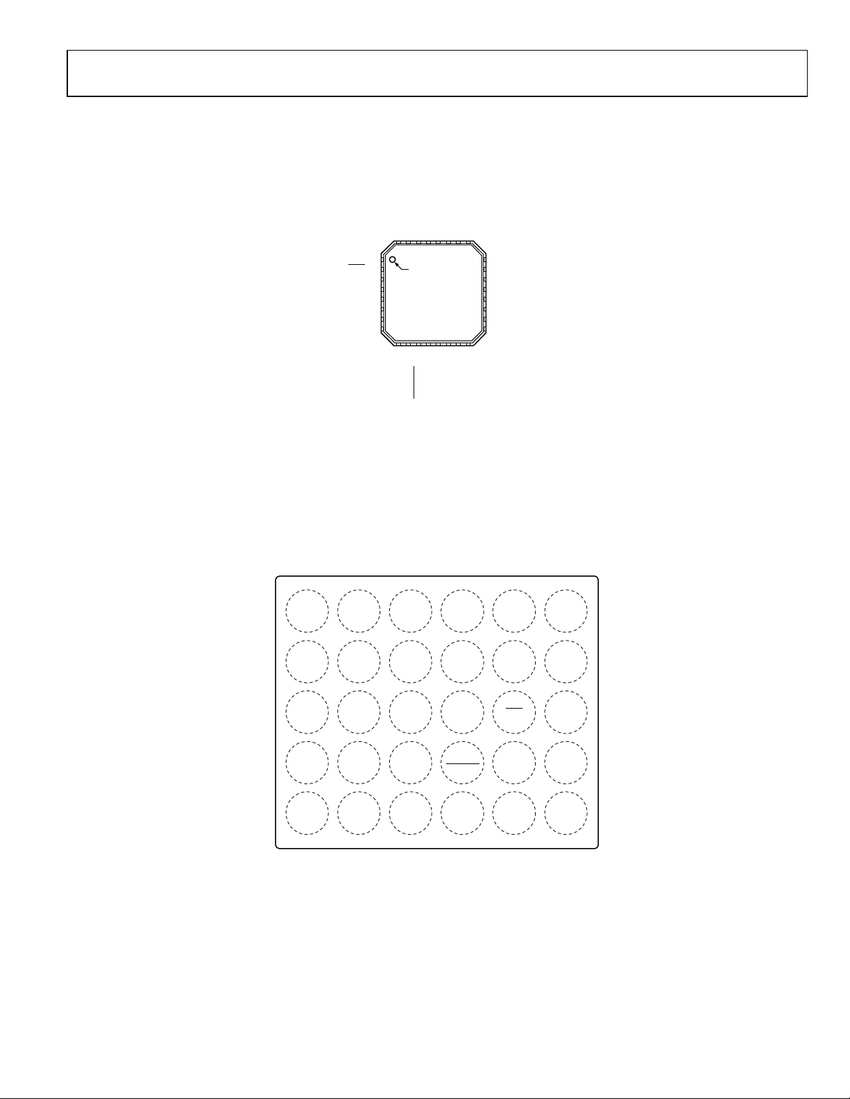
PIN CONFIGURATION AND FUNCTION DESCRIPTIONS
MICBIAS
BEEP
LMIC/LMICN/MICD1
LMICP
RMICP
RMIC/RMICN/MICD2
AOUTL
AOUTR
27
26
25
29
28
31
30
32
1CM
PIN 1
2PDN
INDICATOR
3AGND1
4AVDD1
ADAU1381
5DVDDOUT
6DGND
7GPIO
8SCL/CCLK
NOTES
1. NC = NO CONNECT.
2. THE EXPOSED PAD IS CONNECTED INTERNALLY TO THE
ADAU1381 GROUNDS. F OR INCREASED RELIABILIT Y OF THE
SOLDER JOINTS AND MAXIMUM THERMAL CAPABILITY, IT IS
RECOMMENDED THAT THE PAD BE SOL DE RE D TO THE
GROUND PLANE.
TOP VIEW
(Not to Scale)
9
11
12
10
IOVDD
SDA/COUT
ADDR0/CDATA
ADDR1/CLATCH
13
DAC_SDATA/GPIO0
24 NC
23 AGND2
22 SPP
21 NC
20 SPN
19 AVDD2
18 MCKO
17 MCKI
14
15
16
BCLK/GPIO2
LRCLK/GPIO3
ADC_SDATA/GPIO1
08313-007
Figure 7. 32-Lead LFCSP Pin Configuration
1
AGND2 AOUTL RMICP
A
SPP AOUTR
B
234
RMIC/
RMICN/
MICD2
LMIC/
LIMICN/
MICD1
LMICP BEEP AGND1
MICBIAS CM
56
C
AVDD2 MCKO
D
MCKI
E
SPN
LRCLK/
GPIO3
BCLK/
GPIO2
ADDR0/
CDATA
ADC_
SDATA/
GPIO1
DAC_
SDATA/
GPIO0
(BALL SIDE DOWN)
ADDR1/
CLATCH
TOP VIEW
Not to Scale
SCL/
CCLK
IOVDD
PDN AVDD1
GPIO DVDDOUT
SDA/
COUT
DGND
8313-008
Figure 8. 30-Ball, 6 × 5 WLCSP Pin Configuration (Bottom View)
Rev. B | Page 15 of 84
ADAU1381
Table 10. Pin Function Descriptions
Pin No.
LFCSP WLCSP Mnemonic Type1 Description
1 A6 CM A_OUT
2 C5
PDN
A_IN
3 B6 AGND1 PWR Analog Ground.
4 C6 AVDD1 PWR Analog Power Supply. Should be equivalent to AVDD2.
5 D6 DVDDOUT PWR
6 E6 DGND PWR Digital Ground.
7 D5 GPIO D_IO Dedicated General-Purpose Input/Output.
8 C4 SCL/CCLK D_IN I2C Clock/SPI Clock.
9 E5 SDA/COUT D_IO I2C Data/SPI Data Output.
10 C3 ADDR0/CDATA D_IN I2C Address 0/SPI Data Input.
11 D4
ADDR1/CLATCH
D_IN I
12 E4 IOVDD PWR
13 E3 DAC_SDATA/GPIO0 D_IO DAC Serial Input Data/General-Purpose Input and Output.
14 D3 ADC_SDATA/GPIO1 D_IO ADC Serial Output Data/General-Purpose Input and Output.
15 E2 BCLK/GPIO2 D_IO Serial Data Port Bit Clock/General-Purpose Input and Output.
16 C2 LRCLK/GPIO3 D_IO Serial Data Port Frame Clock/General-Purpose Input and Output.
17 E1 MCKI D_IN Master Clock Input.
18 D2 MCKO D_OUT Master Clock Output.
19 D1 AVDD2 PWR Analog Power Supply. Should be equivalent to AVDD1.
20 C1 SPN A_OUT Speaker Amplifier Negative Signal Output.
21 N/A NC No Connect.
22 B1 SPP A_OUT Speaker Amplifier Positive Signal Output.
23 A1 AGND2 PWR Speaker Amplifier Ground.
24 N/A NC No Connect.
25 B2 AOUTR A_OUT Line Output Amplifier, Right Channel.
26 A2 AOUTL A_OUT Line Output Amplifier, Left Channel.
27 B3 RMIC/RMICN/MICD2 A_IN
28 A3 RMICP A_IN Right Channel Input from Positive Pseudo Differential Source.
29 B4 LMICP A_IN Left Channel Input from Positive Pseudo Differential Source.
30 A4 LMIC/LMICN/MICD1 A_IN
31 B5 BEEP A_IN Beep Signal Input.
32 A5 MICBIAS PWR Microphone Bias.
THERM_PAD
(Exposed Pad)
1
A_OUT = analog output, A_IN = analog input, PWR = power, D_IO = digital input/output, D_OUT = digital output, and D_IN = digital input.
VDD/2 V Common-Mode Reference. A 10 F to 47 F decoupling capacitor should be
connected between this pin and ground to reduce crosstalk between the ADCs and
DACs. The material of the capacitors is not critical. This pin can be used to bias external
analog circuits, as long as they are not drawing current from CM (for example, the
noninverting input of an op amp).
Power-Down. Connecting this pin to GND powers down the chip. Resides in AVDD1
domain.
Digital Core Supply Decoupling Point. The digital supply is generated from an onboard regulator and does not require an external supply. DVDDOUT should be
decoupled to DGND with a 100 nF capacitor.
2
C Address 1/SPI Latch Signal.
Supply for Digital Input and Output Pins. The digital output pins are supplied from
IOVDD, which sets the highest allowed input voltage for the digital input pins. The
current draw of this pin is variable because it is dependent on the loads of the digital
outputs. IOVDD should be decoupled to DGND with a 100 nF capacitor.
Right Channel Input from Single-Ended Source/Right Channel Input from Negative
Pseudo Differential Source/Digital Microphone Input 2.
Left Channel Input from Single-Ended Source/Left Channel Input from Negative
Pseudo Differential Source/Digital Microphone Input 1.
Exposed Pad. The exposed pad is connected internally to the ADAU1381 grounds. For
increased reliability of the solder joints and maximum thermal capability, it is
recommended that the pad be soldered to the ground plane.
Rev. B | Page 16 of 84
ADAU1381
TYPICAL PERFORMANCE CHARACTERISTICS
0
–10
–20
–30
–40
–50
–60
MAGNITUDE (dBFS)
–70
–80
–90
–100
0 0.1 0.2 0.3 0.4 0.5 0.6 0.7 0.8 0.9 1.0
FREQUENCY (NO RM ALIZED TO
f
)
S
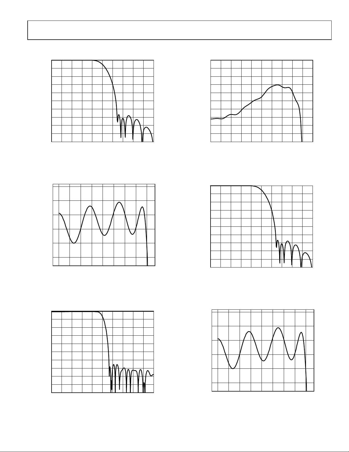
Figure 9. ADC Decimation Filter, 64× Oversampling,
Normalized to f
S
08313-009
0.10
0.08
0.06
0.04
0.02
0
–0.02
MAGNITUDE (dBFS)
–0.04
–0.06
–0.08
–0.10
0 0.05 0.10 0.15 0.20 0.25 0.30 0.35 0.40 0.45 0.50
FREQUENCY (NORMALIZED TO
f
)
S
Figure 12. ADC Decimation Filter Pass-Band Ripple, 128× Oversampling,
Normalized to f
S
08313-012
0.04
0.02
0
–0.02
MAGNITUDE (dBFS)
–0.04
–0.06
0.400.350.300.250.200.150.100.050
FREQUENCY (NORMALIZED TO
f
)
S
Figure 10. ADC Decimation Filter Pass-Band Ripple, 64× Oversampling,
Normalized to f
0
–10
–20
–30
–40
–50
–60
MAGNITUDE (d BF S)
–70
–80
–90
–100
0 0.1 0.2 0.3 0.4 0.5 0.6 0.7 0.8 0.9 1.0
FREQUENCY (NO RM ALIZED TO
S
f
)
S
Figure 11. ADC Decimation Filter, 128× Oversampling,
Normalized to f
S
0
–10
–20
–30
–40
–50
–60
MAGNITUDE (d BFS)
–70
–80
–90
–100
0 0.1 0.2 0.3 0.4 0.5 0.6 0.7 0.8 0.9 1.0
08313-010
FREQUENCY (NO RM ALIZED TO
f
)
S
08313-013
Figure 13. ADC Decimation Filter, Double-Rate Mode,
Normalized to f
0.04
0.02
0
–0.02
MAGNITUDE (dBFS)
–0.04
–0.06
08313-011
14. ADC Decimation Filter Pass-Band Ripple, Double-Rate Mode,
Figure
FREQUENCY (NORMALIZED TO
Normalized to f
S
0.400.350.300.250.200.150.100.050
f
)
S
S
08313-014
Rev. B | Page 17 of 84
ADAU1381
0
–10
–20
–30
–40
–50
–60
MAGNITUDE (dBFS)
–70
–80
–90
–100
0 0.1 0.2 0.3 0.4 0.5 0.6 0.7 0.8 0.9 1.0
FREQUENCY (NO RM ALIZED TO
f
)
S
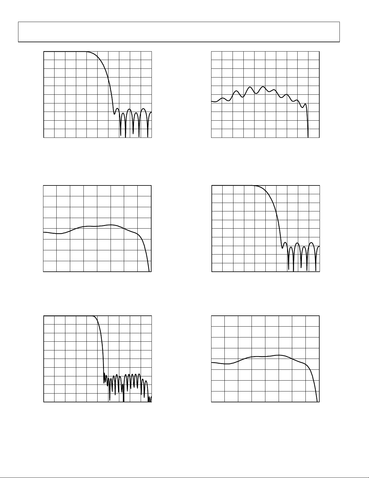
Figure 15. DAC Interpolation Filter, 64× Oversampling,
Normalized to f
S
08313-015
0.05
0.04
0.03
0.02
0.01
0
–0.01
MAGNITUDE (dBFS)
–0.02
–0.03
–0.04
–0.05
0 0.05 0.10 0.15 0.20 0.25 0.30 0.35 0.40 0.45 0.50
FREQUENCY (NORMALIZED TO
f
)
S
Figure 18. DAC Interpolation Filter Pass-Band Ripple, 128× Oversampling,
Normalized to f
S
08313-018
0.20
0.15
0.10
0.05
0
–0.05
MAGNITUDE (dBFS)
–0.10
–0.15
–0.20
0 0.05 0.10 0.15 0.20 0.25 0.30 0.35 0.40
FREQUENCY (NORMALIZED TO
f
)
S
Figure 16. DAC Interpolation Filter Pass-Band Ripple, 64× Oversampling,
Normalized to f
0
–10
–20
–30
–40
–50
–60
MAGNITUDE (dBFS)
–70
–80
–90
–100
0 0.1 0.2 0.3 0.4 0.5 0.6 0.7 0.8 0.9 1.0
FREQUENCY (NO RM ALIZED TO
S
f
)
S
08313-017
Figure 17. DAC Interpolation Filter, 128× Oversampling,
Normalized to f
S
0
–10
–20
–30
–40
–50
–60
MAGNITUDE (dBFS)
–70
–80
–90
–100
0 0.1 0.2 0.3 0.4 0.5 0.6 0.7 0.8 0.9 1.0
08313-016
FREQUENCY (NO RM ALIZED TO
f
)
S
08313-019
Figure 19. DAC Interpolation Filter, Double-Rate Mode,
Normalized to f
0.20
0.15
0.10
0.05
0
–0.05
MAGNITUDE (dBFS)
–0.10
–0.15
–0.20
0 0.05 0.10 0.15 0.20 0.25 0.30 0.35 0.40
FREQUENCY (NORMALIZED TO
S
f
)
S
08313-020
Figure 20. DAC Interpolation Filter Pass-Band Ripple, Double-Rate Mode,
Normalized to f
S
Rev. B | Page 18 of 84
ADAU1381
0
–10
–20
–30
–40
–50
–60
THD + N (dB)
–70
–80
–90
–100
SPEAKER OUTPUT P O WER (mW)
600100101
08313-121
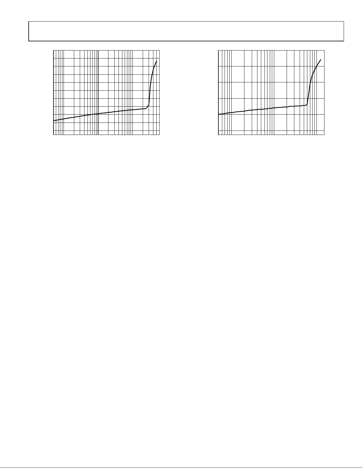
Figure 21. THD + N vs. Speaker Output Power, 8 Ω Load, 3.3 V Supply Figure 22. THD + N vs. Speaker Output Power, 8 Ω Load, 1.8 V Supply
THD + N (dB)
–20
–40
–60
–80
–100
0
SPEAKER OUTPUT P O WER (mW)
100101
08313-122
Rev. B | Page 19 of 84
ADAU1381
A
SYSTEM BLOCK DIAGRAMS
MICBIAS
0.1µF
10µF
0.1µF
IOVDD
+
10µF
0.1µF
VDD1
+
10µF
0.1µF
AVDD2
+
47µF
+
8Ω
0.1µF
–
+
SPEAKER
OUT
DIFFERENTIAL INPUT
(LEFT)
49.9kΩ
49.9kΩ
DIFFERENTIAL INPUT
(RIGHT)
49.9kΩ
49.9kΩ
EXTERNAL
BEEP INPUT
EXTERNAL
MCLK SOURCE
MCKO
PDN
10µF
10µF
10µF
10µF
10µF
49.9Ω
2.2pF
49.9Ω
IOVDD
MICBIAS
LMIC/LMICN/MICD1
LMICP
ADAU1381
RMIC/RMICN/MICD2
RMICP
BEEP
MCKI
MCKO
PDN
THERM_PAD
(EXPOSED PAD)
AVDD1
DVDDOUT
DAC_SDATA/GPIO0
ADC_SDATA/GPIO1
BCLK/GPIO2
LRCLK/GPIO3
ADDR1/CLATCH
ADDR0/CDATA
DGND
AGND1
SPN
SPP
AOUTL
AOUTR
CM
GPIO
SDA/COUT
SCL/CCLK
AGND2
AVDD2
+
100nF 10µF
SERIAL
DATA
SYSTEM
CONTROLLER
10kΩ
10kΩ
GPIO
100pF
10kΩ
100pF
10kΩ
STEREO
HEADPHONE
AMPLIFIER
STEREO SINGLE-ENDED
HEADPHONE OUTP UT
LEFT_OUT
220µF
10Ω
+
10kΩ
10kΩ
220µF
10Ω
+
RIGHT_OUT
08313-021
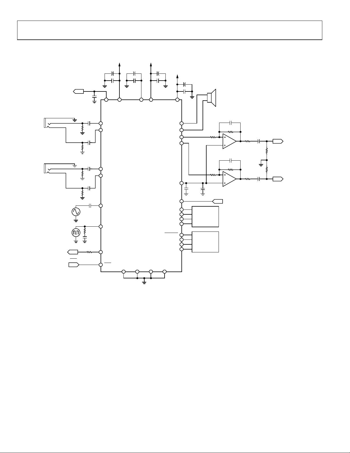
Figure 23. System Block Diagram with Differential Inputs
Rev. B | Page 20 of 84
ADAU1381
A
A
A
MICBIAS
0.1µF
MICBIAS
49.9kΩ
49.9kΩ
EXTERNAL
BEEP INPUT
EXTERNAL
0.1µF
10µF
MICBIAS
0.1µF
10µF
MCKO
PDN
CM
CM
10µF
49.9Ω
2.2pF
49.9Ω
NALOG
MIC 1
NALOG
MIC 2
2kΩ
2kΩ
MCLK SOURCE
IOVDD
10µF
0.1µF
MICBIAS
LMIC/LMICN/MICD1
LMICP
10µF
+
0.1µF
IOVDD
ADAU1381
RMIC/RMICN/MICD2
RMICP
BEEP
MCKI
MCKO
PDN
THERM_PAD
(EXPOSED PAD)
VDD1
+
10µF
0.1µF
AVDD1
DVDDOUT
DAC_SDATA/GPIO0
ADC_SDATA/GPIO1
ADDR1/CLATCH
ADDR0/CDATA
DGND
AGND1
AVDD2
+
SPN
SPP
AOUTL
AOUTR
CM
GPIO
BCLK/GPIO2
LRCLK/GPIO3
SDA/COUT
SCL/CCLK
AGND2
47µF
0.1µF
AVDD2
+
–
+
10kΩ
10kΩ
+
100nF 10µF
SERIAL
DATA
SYSTEM
CONTROLLER
CM
GPIO
8Ω
SPEAKER
OUT
100pF
10kΩ
100pF
10kΩ
STEREO
HEADPHONE
AMPLIFIER
STEREO SINGLE-ENDED
HEADPHONE OUTP UT
LEFT_OUT
220µF
10Ω
+
10kΩ
10kΩ
220µF
10Ω
+
RIGHT_OUT
08313-022
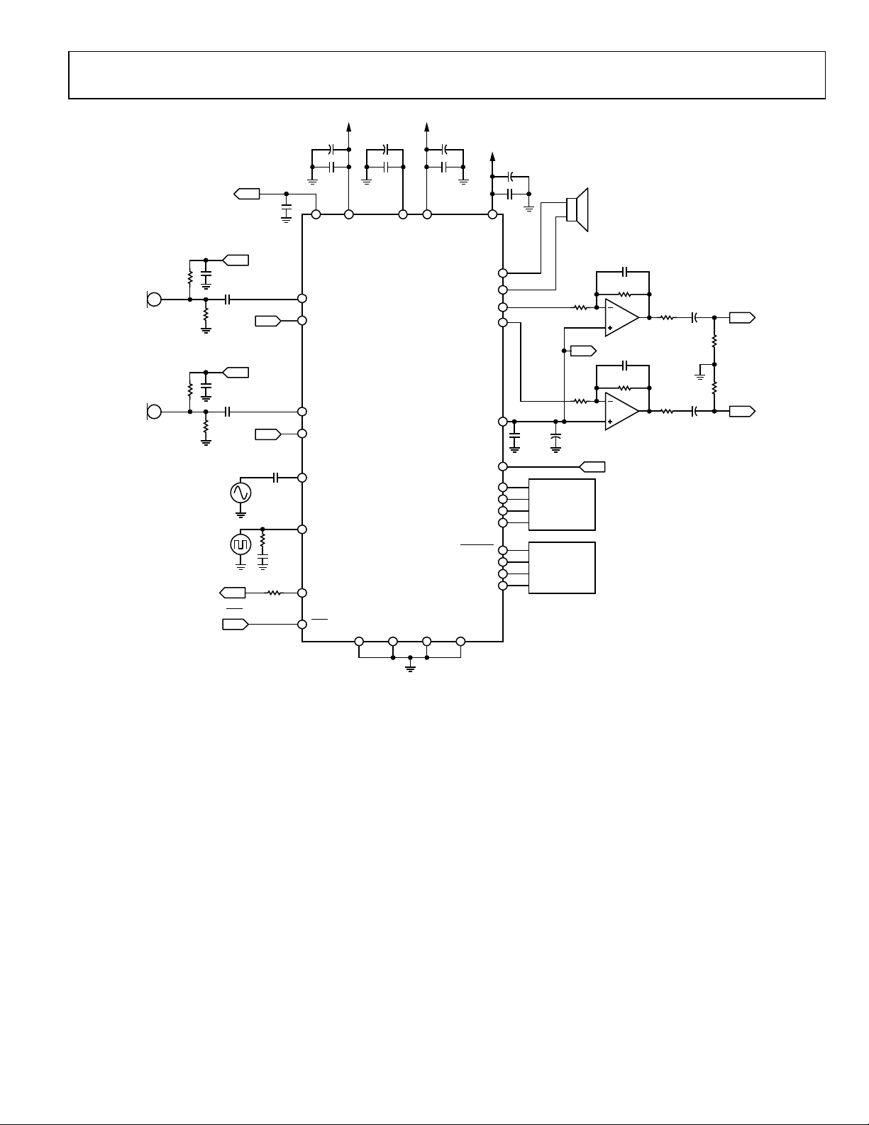
Figure 24. System Block Diagram with Analog Microphone Inputs
Rev. B | Page 21 of 84

ADAU1381
A
SINGLE-ENDED
STEREO INPUT
MCLK SOURCE
1kΩ
49.9kΩ
1kΩ
49.9kΩ
EXTERNAL
BEEP INPUT
EXTERNAL
MICBIAS
10µF
10µF
MCKO
PDN
0.1µF
CM
CM
10µF
49.9Ω
49.9Ω
2.2pF
IOVDD
10µF
0.1µF
MICBIAS
LMIC/LMICN/MICD1
LMICP
10µF
+
0.1µF
IOVDD
ADAU1381
RMIC/RMICN/MICD2
RMICP
BEEP
MCKI
MCKO
PDN
THERM_PAD
(EXPOSED PAD)
VDD1
+
10µF
0.1µF
AVDD1
DVDDOUT
DAC_SDATA/GPIO0
ADC_SDATA/GPIO1
ADDR1/CLATCH
ADDR0/CDATA
DGND
AGND1
AVDD2
+
SPN
SPP
AOUTL
AOUTR
CM
GPIO
BCLK/GPIO2
LRCLK/GPIO3
SDA/COUT
SCL/CCLK
AGND2
47µF
0.1µF
AVDD2
+
–
+
+
100nF 10µF
SERIAL
DATA
SYSTEM
CONTROLLER
10kΩ
CM
10kΩ
8Ω
SPEAKER
OUT
GPIO
100pF
10kΩ
100pF
10kΩ
STEREO
HEADPHONE
AMPLIFIER
STEREO SINGLE-ENDED
HEADPHONE OUTPUT
LEFT_OUT
220µF
10Ω
+
10kΩ
10kΩ
220µF
10Ω
+
RIGHT_OUT
08313-023
Figure 25. System Block Diagram with Single-Ended Stereo Line Inputs
Rev. B | Page 22 of 84
ADAU1381
A
MICBIAS
0.1µF
BCLK OR MCLKO
STEREO DIGI T AL
MIC INPUT
1kΩ
10µF
EXTERNAL
BEEP INPUT
EXTERNAL
MCLK SOURCE
MCKO
49.9Ω
2.2pF
49.9Ω
PDN
IOVDD
10µF
0.1µF
MICBIAS
LMIC/LMICN/MICD1
LMICP
10µF
+
0.1µF
IOVDD
ADAU1381
RMIC/RMICN/MICD2
RMICP
BEEP
MCKI
MCKO
PDN
THERM_PAD
(EXPOSED PAD)
VDD1
+
10µF
0.1µF
AVDD1
DVDDOUT
DAC_SDATA/GPIO0
ADC_SDATA/GPIO1
ADDR1/CLATCH
ADDR0/CDATA
DGND
AGND1
AVDD2
+
SPN
SPP
AOUTL
AOUTR
CM
GPIO
BCLK/GPIO2
LRCLK/GPIO3
SDA/COUT
SCL/CCLK
AGND2
47µF
0.1µF
AVDD2
+
–
+
10kΩ
10kΩ
+
100nF 10µF
SERIAL
DATA
SYSTEM
CONTROLLER
8Ω
SPEAKER
OUT
GPIO
100pF
10kΩ
100pF
10kΩ
STEREO
HEADPHONE
AMPLIFIER
BCLK
STEREO SINGLE-ENDED
HEADPHONE OUTP UT
LEFT_OUT
220µF
10Ω
+
10kΩ
10kΩ
220µF
10Ω
+
RIGHT_OUT
08313-024
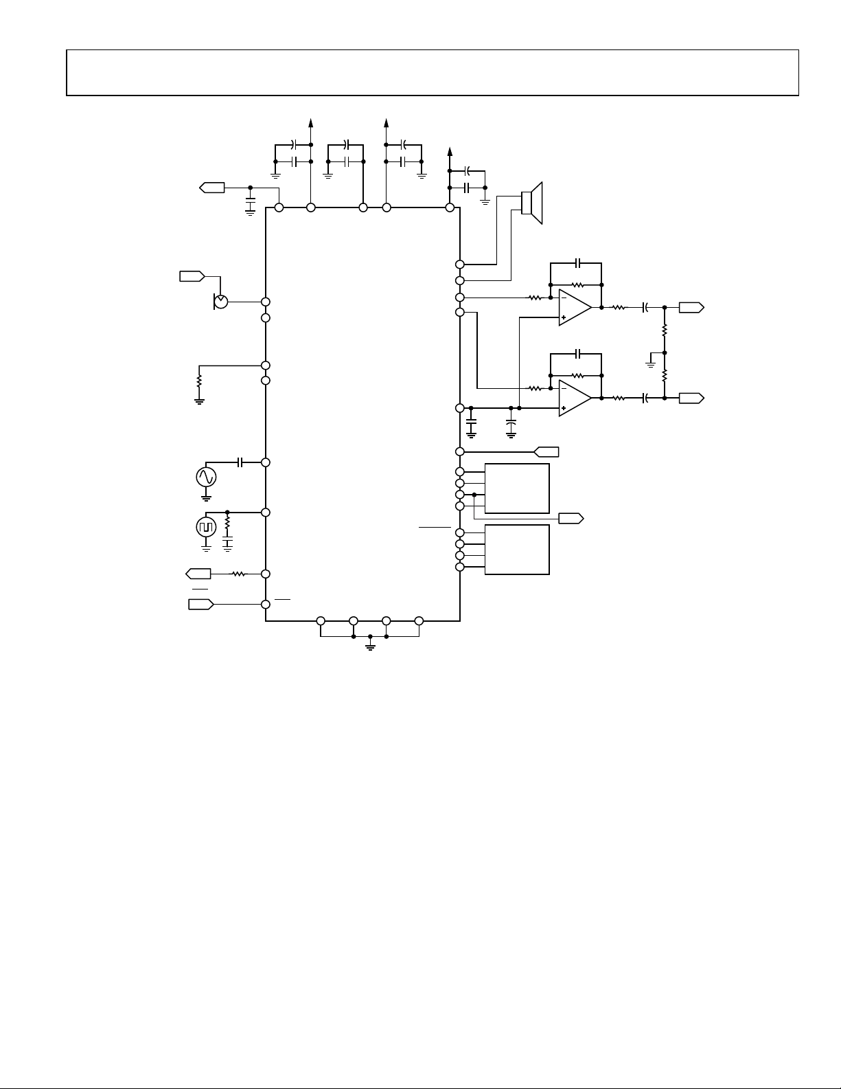
Figure 26. System Block Diagram with Stereo Digital Microphone Inputs
Rev. B | Page 23 of 84

ADAU1381
THEORY OF OPERATION
The ADAU1381 is a low power audio codec with an integrated,
fixed-function audio processing sound engine. It is an all-in-one
package that offers high quality audio, low power, small size, and
many advanced features. The stereo ADC and stereo DAC each
have a dynamic range (DNR) performance of at least 96.5 dB and
a total harmonic distortion plus noise (THD + N) performance
of at least −90 dB. The serial data port is compatible with I
justified, right-justified, and TDM modes for interfacing to digital
audio data. The operating voltage range is 1.8 V to 3.65 V, with
an on-board regulator generating the internal digital supply voltage.
The record path includes very flexible input configurations that
can accept differential or single-ended analog microphone inputs
as well as two stereo digital microphone inputs. There is also a
beep input pin (BEEP) dedicated to analog beep signals that are
common in digital still camera applications. A microphone bias
pin that can power electrets-type microphones is also available.
Each input signal has its own programmable gain amplifier (PGA)
for input volume adjustment. An automatic level control (ALC)
is built into the sound engine to maintain a constant input recording volume.
The ADCs and DACs are high quality, 24-bit Σ- converters
that operate at selectable 64× or 128× oversampling rates. The
base sampling rate of the converters is set by the input clock rate
and can be further scaled with the converter control register
settings. The converters can operate at sampling frequencies
from 8 kHz to 96 kHz. The ADCs and DACs also include very
fine-step digital volume controls.
2
S, left-
The playback path allows input signals and DAC outputs to be
mixed into speaker and/or line outputs. The speaker driver is
capable of driving 400 mW into an 8 Ω load.
The fixed-function sound engine contains a digital audio
processing flow optimized for digital still camera stereo audio
processing. However, the flexibility offered by the built-in
sound engine allows this codec to be used for a wide variety of
low power applications. Signal processing blocks included in the
sound engine include the following:
• Wind noise detection and autofiltering
• Dual-band compression with programmable crossover,
compression curves, and timing
• Programmable multiband equalizer
• Configurable notch filter
• Enhanced stereo capture algorithm
• Automatic level control
• Digital volume control
• Multiplexers for signal routing
The ADAU1381 can generate its internal clocks from a wide
range of input clocks by using the on-board fractional PLL.
The PLL accepts inputs from 11 MHz to 20 MHz.
The ADAU1381 is provided in a small, 32-lead, 5 mm × 5 mm
lead frame chip scale package (LFCSP) with an exposed bottom
pad, or a 30-ball (6 × 5 bump), 3.4 mm × 2.64 mm wafer level
chip scale package (WLCSP).
Rev. B | Page 24 of 84
ADAU1381
STARTUP, INITIALIZATION, AND POWER
This section details the procedure for setting up the ADAU1381
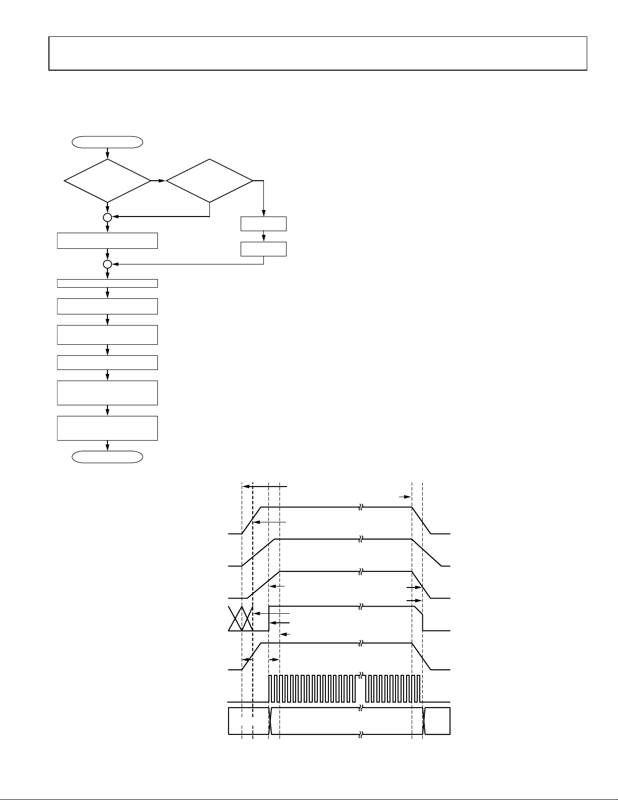
properly. Figure 27 provides an overview of how to initialize the IC.
START
ARE AVDD1 AND AVDD2
SUPPLIED SEPARATELY?
NO
SUPPLY POWER TO AVDD1/AVDD2
PINS SIMULTANEOUSLY
CAN AVDD1 AND AVDD2
BE SIMULTANEOUSLY
SUPPLIED?
YES
NOYES
SUPPLY POWER
TO AVDD1
SUPPLY POWER
TO AVDD2
POWER-UP SEQUENCE
If AVDD1 and AVDD2 are from the same supply, they can
power up simultaneously. If AVDD1 and AVDD2 are from
separate supplies, then AVDD1 should be powered up first.
IOVDD should be applied simultaneously with AVDD1, if
possible.
The ADAU1381 uses a power-on reset (POR) circuit to reset the
registers upon power-up. The POR monitors the DVDDOUT
pin and generates a reset signal whenever power is applied to
the chip. During the reset, the ADAU1381 is set to the default
values documented in the register map (see the Control Register
Map section).
SUPPLY POWER TO I OVDD
WAIT 14ms FOR POWER-ON RESET
AND INITIALIZATION ROM BOOT
CONFIGURE CLOCK GENERATION
REGISTER 16384 (0x4000)
AND REGISTER 16386 (0x4002)
WAIT FOR PLL LOCK
(2.4ms TO 3.5ms)
ENABLE DIG ITAL POW E R T O
FUNCTIONA L SUBSY ST EMS
REGISTER 16512 (0x4080)
AND REGISTER 16513 (0x4081)
SET UP SOUND ENGINE REG ISTERS
FOR CUSTOMI ZED SIGNAL PATH
(INCLUDING VOLUME, SAMPLE RATES,
FILTER COEFFICIENTS)
INITIALIZATION
COMPLETE
Figure 27. Initialization Sequence
AVDD1
AVDD2
DVDDOUT
POWER-UP
(INTERNAL
SIGNAL)
IOVDD
14ms
The POR is also used to prevent clicks and pops on the speaker
driver output. The power-up sequencing and timing involved is
described in Figure 28 in this section, and in Figure 36 and
Figure 37 of the Speaker Output section.
A self-boot ROM initializes the memories after the POR has
completed. When the self-boot sequence is complete, the control
registers are accessible via the I
then be configured as required for the application. Typically,
with a 10 F capacitor on AVDD1, the power supply ramp-up,
POR, and self-boot combined take approximately 14 ms.
08313-025
MAIN SUPPLY ENABLED
MAIN SUPPLY DISABLED
1.5V
1.5V
1.35V
ACTIVE
POR ACTIVATES
POR COMPLETE/SELF-BOOT INITIATES
SELF-BOOT COMPLETE/MEMORY
IS ACCESSIBLE
0.95V
POR
2
C/SPI control port and should
INTERNAL MCLK
(NOT TO SCALE)
INPUT/OUTPUT
PINS
Figure 28. Power-Up and Power-Down Sequence Timing Diagram
ACTIVE
HIGH-ZHIGH-Z
08313-026
Rev. B | Page 25 of 84

ADAU1381
CLOCK GENERATION AND MANAGEMENT
The ADAU1381 uses a flexible clocking scheme that enables the
use of many different input clock rates. The PLL can be bypassed
or used, resulting in two different approaches to clock management. For more information about clocking schemes, PLL
configuration, and sampling rates, see the Clocking and
Sampling Rates section.
Case 1: PLL Is Bypassed
If the PLL is bypassed, the core clock is derived directly from
the master clock (MCLK) input. The rate of this clock must be
set properly in Register 16384 (0x4000), clock control, Bits[2:1],
input master clock frequency. When the PLL is bypassed,
supported external clock rates are 256 × f
and 1024 × f
of the chip is off until Register 16384 (0x4000), clock control,
Bit 0, core clock enable, is set to 1.
, where fS is the base sampling rate. The core clock
S
Case 2: PLL Is Used
The core clock to the entire chip is off during the PLL lock
acquisition period. The user can poll the lock bit to determine
when the PLL has locked. After lock is acquired, the ADAU1381
can be started by setting Register 16384 (0x4000), clock control,
Bit 0, core clock enable, to 1.This bit enables the core clock to all
the internal functional blocks of the ADAU1381.
PLL Lock Acquisition
During the lock acquisition period, only Register 16384 (0x4000),
clock control, and Register 16386 (0x4002), PLL control, are
accessible through the control port. Reading from or writing to
any other address is prohibited until Register 16384 (0x4000),
clock control, Bit 0, core clock enable, and Register 16386 (0x4002),
PLL control, Bit 1, PLL lock, are set to 1.
Register 16386 (0x4002), PLL control, is a 48-bit register for which
all bits must be written with a single continuous write to the
control port.
The PLL lock time is dependent on the MCLK rate. Typical lock
times are provided in Tab le 1 1.
Table 11. PLL Lock Time
PLL Mode MCLK Frequency Lock Time (Typical)
Fractional 12 MHz 3.0 ms
Integer 12.288 MHz 2.96 ms
Fractional 13 MHz 2.4 ms
Fractional 14.4 MHz 2.4 ms
Fractional 19.2 MHz 2.98 ms
Fractional 19.68 MHz 2.98 ms
Fractional 19.8 MHz 2.98 ms
, 512 × fS, 768 × fS,
S
ENABLING DIGITAL POWER TO FUNCTIONAL SUBSYSTEMS
To power subsystems in the device, they must be enabled using
Register 16512 (0x4080), Digital Power-Down 0, and Register
16513 (0x4081), Digital Power-Down 1. The exact settings depend
on the application. However, to proceed with the initialization
sequence and access the RAMs and registers of the ADAU1381,
Register 16512 (0x4080), Digital Power-Down 0, Bit 6, memory
controller, and Bit 0, sound engine, must be enabled.
SETTING UP THE SOUND ENGINE
After the PLL has locked, the ADAU1381 is in an operational
state, and the control port can be used to configure the sound
engine. For more information, see the Sound Engine section.
POWER REDUCTION MODES
Sections of the ADAU1381 chip can be turned on and off as
needed to reduce power consumption. These include the ADCs,
the DACs, and the PLL.
In addition, some functions can be set in the registers to operate
in power saving, normal, or enhanced performance operation.
See the respective portions of the General-Purpose Input/Outputs
section for more information.
Each digital filter of the ADCs and DACs can be set to a 64× or
128× (default) oversampling ratio. Setting the oversampling ratio
to 64× lowers power consumption with a minimal impact on
performance. See the Typical Performance Characteristics section
and the Typical Power Management Measureme nts section for
specifications and graphs of the filters.
Detailed information regarding individual power reduction control
registers can be found in the Control Register Map section of this
document.
Power-Down Pin (
The power-down pin provides a simple hardware-based
method for initiating low power mode without requiring access
via the control port. When the
potential as ground, the internal digital regulator is disabled
and the device ceases to function, with power consumption
dropping to a very low level. The common-mode voltage sinks,
and all internal memories and registers lose their contents.
When the
AVDD1, the device reinitializes in its default state, as described
in the section. Power-Up Sequence
PDN
PDN
)
PDN
pin is lowered to the same
pin is raised back to the same potential as
POWER-DOWN SEQUENCE
When powering down the device, the IOVDD, AVDD1, and
AVDD2 supplies should be disabled at the same time, if possible,
but only after the analog and speaker outputs have been muted. If
the supplies cannot be disabled simultaneously, the preferred
sequence is IOVDD first, AVDD2 second, and AVDD1 last.
Rev. B | Page 26 of 84
 Loading...