


200 MHz Dual Integrated DCL with Level
www.BDTIC.com/ADI
Setting DACs, Per Pin PMU, and Per Chip VHH
FEATURES
Driver
3-level driver with high-Z mode and built-in clamps
Precision trimmed output resistance
Low leakage mode (typically <10 nA)
Voltage range: up to −2.0 V to +6.0 V
2.4 ns minimum pulse width, 2 V terminated
Comparator
Window and differential comparator
500 MHz input equivalent bandwidth
Load
±12 mA maximum current capability
Per pin PMU
Force voltage range: up to −2.0 V to +6.0 V
5 current ranges: 32 mA, 2 mA, 200 μA, 20 μA, 2 μA
Levels
14-bit DAC for DCL levels
Typically < ±5 mV INL (calibrated)
16-bit DAC for PMU levels
Typically < ±1.5 mV INL (calibrated) linearity in FV mode
HVOUT output buffer
0 V to 13.5 V output range
84-lead, 9 mm × 9 mm, CSP_BGA package
900 mW per channel with no load
APPLICATIONS
Automatic test equipment
Semiconductor test systems
Board test systems
Instrumentation and characterization equipment
ADATE304
GENERAL DESCRIPTION
The ADATE304 is a complete, single-chip solution that performs
the pin electronic functions of the driver, the comparator, and
the active load (DCL), per pin PMU, and dc levels for ATE applications. The device also contains an HVOUT driver with a VHH
buffer capable of generating up to 13.5 V.
The driver features three active states: data high mode, data low
mode, and term mode, as well as an inhibit state. The inhibit
state, in conjunction with the integrated dynamic clamp, facilitates the implementation of a high speed active termination.
The ADATE304 supports two output voltage ranges: −2.0 V
to +6.0 V and −1.25 V to +6.75 V by adjusting the positive and
negative supply voltages.
Each channel of the ADATE304 features a high speed window
comparator per pin for functional testing, as well as a per pin
PMU with FV, or FI and MV, or MI functions. All necessary dc
levels for DCL functions are generated by on-chip 14-bit DACs.
The per pin PMU features an on-chip 16-bit DAC for high
accuracy and contains integrated range resistors to minimize
external component counts.
The ADATE304 uses a serial bus to program all functional blocks
and has an on-board temperature sensor for monitoring the
device temperature.
Rev. 0
Information furnished by Analog Devices is believed to be accurate and reliable. However, no
responsibility is assumed by Analog Devices for its use, nor for any infringements of patents or other
rights of third parties that may result from its use. Specifications subject to change without notice. No
license is granted by implication or otherwise under any patent or patent rights of Analog Devices.
Trademarks and registered trademarks are the property of their respective owners.
One Technology Way, P.O. Box 9106, Norwood, MA 02062-9106, U.S.A.
Tel: 781.329.4700 www.analog.com
Fax: 781.461.3113 ©2008 Analog Devices, Inc. All rights reserved.

ADATE304
www.BDTIC.com/ADI
TABLE OF CONTENTS
Features .............................................................................................. 1
Applications ....................................................................................... 1
General Description ......................................................................... 1
Revision History ............................................................................... 2
Functional Block Diagram .............................................................. 3
Specifications ..................................................................................... 4
Total Function ............................................................................... 4
Driver ............................................................................................. 5
Reflection Clamp .......................................................................... 7
Normal Window Comparator .................................................... 7
Differential Comparator .............................................................. 9
Active Load .................................................................................. 10
PMU ............................................................................................. 11
External Sense (PMUS_CHx) ................................................... 16
DUTGND Input ......................................................................... 16
Serial Peripheral Interface ......................................................... 16
HVOUT Driver ........................................................................... 17
Overvoltage Detector (OVD) ................................................... 18
16-Bit DAC Monitor MUX ....................................................... 18
Absolute Maximum Ratings .......................................................... 19
Thermal Resistance .................................................................... 19
Explanation of Test Levels ......................................................... 19
ESD Caution................................................................................ 19
Pin Configuration and Function Descriptions ........................... 20
Typical Performance Characteristics ........................................... 23
SPI Details ....................................................................................... 33
Definition of SPI Word .............................................................. 34
Write Operation.......................................................................... 35
Read Operation........................................................................... 36
Reset Operation .......................................................................... 37
Register Map ................................................................................... 38
Details of Registers ......................................................................... 39
User Information ............................................................................ 41
Power Supply Considerations ................................................... 41
Truth Tables................................................................................. 41
Details of DACs vs. Levels ......................................................... 43
Recommended PMU Mode Switching Sequences ................. 45
Block Diagrams ............................................................................... 47
Outline Dimensions ....................................................................... 51
Ordering Guide .......................................................................... 51
REVISION HISTORY
10/08—Revision 0: Initial Version
Rev. 0 | Page 2 of 52
ADATE304
www.BDTIC.com/ADI
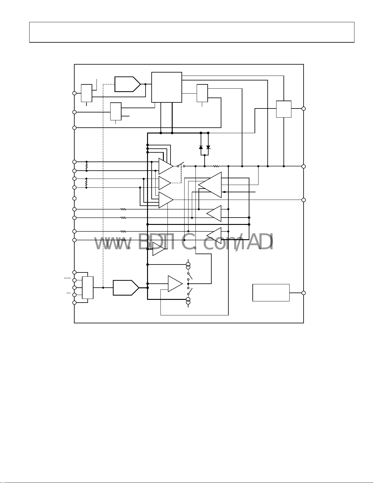
FUNCTIONAL BLOCK DIAGRAM
DAC16_MON
MEASOUT01
PMUS_CH0
DATA0P
DATA0N
RCV0P
RCV0N
COMP_VTT 0
COMP_QH0P
COMP_Q H0N
COMP_QL0P
COMP_QL0N
MUX
*
100
100
CH1
16-BIT DAC
*
MUX
50
CH1
VH
VT
VL
PMU_FLAG
DRV
*
VHH
*
G
PMU
VCLAMPH
MUX
VCLAMPL
VCLAMPH VCLAMPL
R
(TRIMMED)
WINDOW
DIFF.
C
OUT
C
C
SENSE
OVD
FORCE
OVD_CH0
DUT0
*
OTHER CHANNEL
DUT1
HVOUT
VOH
VOL
SDIN
RST
SCLK
CS
SDOUT
*
SPI
*
ONE PER DEVICE.
IOL
VCOM
14-BIT DAC
IOH
ADATE304
TEMPERATURE
SENSOR
*
TEMPSENSE
07279-001
Figure 1. One of Two Channels
Rev. 0 | Page 3 of 52
ADATE304
www.BDTIC.com/ADI
SPECIFICATIONS
Characterization and production tests performed using Power Supply Range 1 (see Table 37). VDD = +10.75 V, VCC = +3.3 V, VSS = −5.00 V,
= +16.75 V, V
V
PLUS
values are at T
= 55°C, where TJ corresponds to the internal temperature sensor and the temperature coefficients are measured at TJ =
J
55°C ± 20°C, unless otherwise noted. Typical values are based on design, simulation analyses, and/or limited bench evaluations. Typical
values are not tested or guaranteed. Test levels are specified in the Explanation of Test Levels section.
TOTAL FUNCTION
Table 1.
Parameter Symbol Min Typ Max Unit
TOTAL FUNCTION
Output Leakage Current
PE Disable Range E −20.0 +5.3 +20.0 nA P −1.25 V < V
PE Disable Range A to Range D 5.3 nA CT −1.25 V < V
High-Z Mode −400 +5.4 +400 nA P −1.25 V < V
Output Capacitance 4 pF S VTERM mode operation
DUT Pin Range −1.25 +6.0 V D
POWER SUPPLIES
Total Supply Range, V
VPLUS Supply V
Positive Supply VDD 10.25 10.75 11.25 V D Defines PSRR conditions
Negative Supply VSS −5.25 −5.00 −4.75 V D Defines PSRR conditions
Logic Supply VCC 3.1 3.3 3.5 V D Defines PSRR conditions
Comparator Termination V
V
Supply Current I
PLUS
4.0 12.7 16.0 mA P HVOUT enabled, RCV active, no load, VHH = 12 V
Logic Supply Current ICC 1.0 2.7 4.0 mA P Quiescent (SPI is static)
Comparator Termination Current I
Positive Supply Current IDD 72 90.5 97 mA P Load power down (IOH = IOL = 0 mA)
Negative Supply Current ISS 100 116 126 mA P Load power down (IOH = IOL = 0 mA)
Total Power Dissipation 1.0 1.6 1.82 W P Load power down (IOH = IOL = 0 mA)
Positive Supply Current IDD 102 120 152 mA P Load active off (IOH = IOL = 12 mA)
Negative Supply Current ISS 130 146 181 mA P Load active off (IOH = IOL = 12 mA)
Total Power Dissipation 1.8 2.2 2.5 W P Load active off (IOH = IOL = 12 mA)
TEMPERATURE MONITORS
Temperature Sensor Gain 10 mV/K CT
Temperature Sensor Accuracy Without
Calibration over 25°C to 100°C
VREF INPUT
Reference Input Voltage Range for
DACs (VREF Pin)
Input Bias Current 0.1 100 μA P Tested with 5 V applied
= +3.3 V, V
COMP_VTT
to VSS 22.5 23.25 V D Defines PSRR conditions
PLUS
= +5.0 V, V
REF
16.25 16.75 17.25 V D Defines PSRR conditions
PLUS
3.3 5.0 V D
COMP_VTT
−1.0 +1.3 +3.0 mA P HVOUT disabled
PLUS
10.0 17 26.0 mA P
COMP_VTT
6 °C CT Temperature voltage available on Pin A1 at all
4.95 5 5.05 V D Referenced to V
= 0.0 V. All default test conditions are as defined in Table 38. All specified
REF_GND
Test
Level Test Conditions/Comments
via SPI; PMU Range E, VCH = 7.0 V, VCL = −2.5 V
SPI; PMU Range A, PMU Range B, PMU Range C,
and PMU Range D, VCH = +7.0 V, VCL = −2.5 V
enabled via SPI; RCV active, VCH = +7.0 V, VCL =
−2.5 V
times and on Pin K1 (MEASOUT01/TEMPSENSE)
when selected (see
DUTx
DUTx
DUTx
< +6.0 V; PMU and PE disabled
< +6.0 V; PMU and PE disabled via
< +6.0 V; PMU disabled and PE
Tab le 24 and Tabl e 36 )
; not referenced to V
REF_GND
DUTGND
Rev. 0 | Page 4 of 52
ADATE304
www.BDTIC.com/ADI
DRIVER
VH − VL ≥ 200 mV (to meet dc and ac specifications).
Table 2.
Parameter Min Typ Max Unit
DC SPECIFICATIONS
High Speed Differential Logic Input
Characteristics (DATAxx, RCVxx)
Input Termination Resistance 92 100 108 Ω P
Input Voltage Differential 0.2 1.0 V PF
Common-Mode Voltage 0.85 2.35 V PF
0.85 3.5 V D
Input Bias Current −20.0 +2.2 +20.0 A P Each pin tested at 2.85 V and 0.35 V while the other high speed
Pin Output Characteristics
Output High Range, VH −1.15 +6.75 V D
Output Low Range, VL −1.25 +6.65 V D
Output Term Range, VT −1.25 +6.75 V D
Functional Amplitude (VH − VL) 0.0 8.0 V D Amplitude can be programmed to VH = VL, accuracy specifica-
DC Output Current Limit Source 75 100 120 mA P Driver high, VH = 6.75 V, short DUTx pin to −1.25 V, measure
DC Output Current Limit Sink −120 −100 −75 mA P Driver low, VL = −1.25 V, short DUTx pin to +6.75 V, measure
Output Resistance, ±50 mA 45.0 47.0 49.0 Ω P Source: driver high, VH = +3.0 V, I
ABSOLUTE ACCURACY VH tests done with VL = −2.5 V and VT= −2.5 V;
VH, VL, VT Uncalibrated Accuracy −250 ±75 +250 mV P Error measured at calibration points of 0 V and 5 V
VH, VL, VT Offset Tempco ±450 V/°C CT Measured at calibration points
VH, VL, VT DNL ±1 mV CT After two-point gain/offset calibration
VH, VL, VT INL −10 ±2.5 +10 mV P After two-point gain/offset calibration; measured over driver
VH, VL, VT Resolution 0.6 +1 mV PF After two-point gain/offset calibration; range/number of DAC
DUTGND Voltage Accuracy −7 ±1.3 +7 mV P Over ±0.1 V range; measured at endpoints of VH, VL, and VT
VH, VL, VT Crosstalk ±2 mV CT
Overall Voltage Accuracy ±10 mV CT Sum of INL, crosstalk, DUTGND, and tempco over ±5°C, after
VH, VL, VT DC PSRR ±15 mV/V CT Measured at calibration points
AC SPECIFICATIONS
Rise/Fall Times Toggle DATAxx
0.2 V Programmed Swing 950 ps CB VH = 0.2 V, VL = 0.0 V, terminated; 20% to 80%
1.0 V Programmed Swing 850 ps CB VH = 1.0 V, VL = 0.0 V, terminated; 20% to 80%
2.0 V Programmed Swing 850 1150 1350 ps CB VH = 3.0 V, VL = 0.0 V, terminated; 20% to 80%
3.0 V Programmed Swing 1500 ps P/CB VH = 3.0 V, VL = 0.0 V, terminated; 20% to 80%
3.0 V Programmed Swing 2000 ps CB VH = 3.0 V, VL = 0.0 V, unterminated; 10% to 90%
5.0 V Programmed Swing 3100 ps CB VH = 5.0V, VL = 0.0 V, unterminated; 10% to 90%
Rise-to-Fall Matching 40 ps CB VH = 3.0 V, VL = 0.0 V, terminated; rise-to-fall within one channel
Test
Level
Test Conditions/Comments
Push 6 mA into xP pins
voltage from xP to xN
pin remains open
tions apply when VH − VL ≥ 200 mV
current
current
sink: driver low, VL = 0.0 V, I
VL tests done with VH = +7.5 V and VT = +7.5 V;
VT tests done with VL = −2.5 V and VH = +7.5 V; unless
otherwise specified
output ranges
bits as measured at calibration points of 0 V and 5 V
functional range
VL = −1.25 V: VH = −1.15 V
VH = +6.75 V: VL = −1.25 V
VT = +1.25 V: VL = −1.25 V
dc crosstalk on VL, VH, VT output level when other driver DACs
are varied
gain/offset calibration
1
, force 1.3 V on xN pins1; measure
1
, calculate resistance (∆V/∆I)
= +1 mA and +50 mA;
DUTx
= −1 mA and −50 mA; ∆V
DUTx
→ +6.75 V, VT = −1.25 V → +6.75 V;
→ +6.65 V, VT = −1.25 V → +6.75 V;
→ +6.65 V, VH = −1.15 V → +6.75 V;
DUT
/∆I
DUT
Rev. 0 | Page 5 of 52
ADATE304
www.BDTIC.com/ADI
Parameter Min Typ Max Unit
Minimum Pulse Width Toggle DATAxx
1.0 V Programmed Swing 1.7 ns CB VH = 1.0 V, VL = 0.0 V, terminated; timing error ± 75 ps
1.7 ns CB VH = 1.0 V, VL = 0.0 V, terminated; less than 10% amplitude
2.0 V Programmed Swing 2.0 ns CB VH = 2.0 V, VL = 0.0 V, terminated; timing error ± 75 ps
2.2 ns CB VH = 2.0 V, VL = 0.0 V, terminated; less than 10% amplitude
3.0 V Programmed Swing 2.7 ns CB VH = 3.0 V, VL = 0.0 V, terminated; timing error ± 75 ps
2.7 ns CB VH = 3.0 V, VL = 0.0 V, terminated; less than 10% amplitude
Maximum Toggle Rate
2.0 V Programmed Swing 200 MHz CB VH = 2.0 V, VH = 0.0 V, terminated, 10% amplitude degradation
Dynamic Performance, Drive
(VH to VL and VL to VH)
Propagation Delay Time 3.0 ns CB VH = 2.0 V, VL = 0.0 V, terminated
Propagation Delay Tempco 3.0 ps/°C CT VH = 2.0 V, VL = 0.0 V, terminated
Delay Matching VH = 2.0 V, VL = 0.0 V, terminated
Edge to Edge 80 ps CB Rising vs. falling
Channel to Channel 30 ps CB Rising vs. rising, falling vs. falling
Delay Change vs. Duty Cycle 30 ps CB VH = 3.0 V, VL = 0.0 V, terminated; 5% to 95% duty cycle; 1 MHz
Overshoot and Undershoot 30 mV CB VH = 3.0 V, VL = 0.0 V, terminated
Settling Time (VH to VL) Toggle DATAxx
To Within 3% of Final Value 4 ns CB VH = 3.0 V, VL = 0.0 V, terminated
To Within 1% of Final Value 25 ns CB VH = 3.0 V, VL = 0.0 V, terminated
Dynamic Performance, VT
(VH or VL to VT and VT to VH or VL)
Propagation Delay Time 3.7 ns CB VH = 3.0 V, VT = 1.5 V, VL = 0.0 V, terminated
Delay Matching, Edge to Edge 150 ps CB VH = 3.0 V, VT = 1.5 V, VL = 0.0 V, terminated; rising vs. falling
Propagation Delay Tempco 4.0 ps/°C CT VH = 3.0 V, VT = 1.5 V, VL = 0.0 V, terminated
Transition Time, Active to VT
and VT to Active
Dynamic Performance, Inhibit
(VH or VL to/from Inhibit)
Propagation Delay Time VH = +1.0 V, VL = −1.0 V, terminated
Active to Inhibit 4.5 ns CB
Inhibit to Active 7.9 ns CB
Transition Time VH =+1.0 V, VL = −1.0 V, terminated; 20% to 80%
Active to Inhibit 2.9 ns CB
Inhibit to Active 0.65 ns CB
I/O Spike 190 mV CB VH = 0.0 V, VL = 0.0 V, terminated
1
The xP pins include DATA0P, DATA1P, RCV0P, and RCV1P; the xN pins include DATA0N, DATA1N, RCV0N, and RCV1N. For example, push 6 mA into the DATA0P pin,
force 1.3 V into DATA0N, and measure the voltage from DATA0P to DATA0N.
Toggle DATAxx
Toggle RCVxx
1.0 ns CB VH = 3.0 V, VT = 1.5 V, VL = 0.0 V, terminated; 20% to 80%
Toggle RCVxx
Test
Level Test Conditions/Comments
degradation
degradation
degradation
Rev. 0 | Page 6 of 52
ADATE304
www.BDTIC.com/ADI
REFLECTION CLAMP
Clamp accuracy specifications apply when VCH > VCL.
Table 3.
Parameter Min Typ Max Unit
VCH
Range −1.0 +6.75 V D
Uncalibrated Accuracy −200 ±50 +200 mV P Driver high-Z, sinking 1 mA; VCH error measured at the
Resolution 0.6 0.75 mV PF Driver high-Z, sinking 1 mA; after two-point gain/offset
DNL ±1 mV CT Driver high-Z, sinking 1 mA; after two-point gain/offset
INL −40 ±2 +40 mV P Driver high-Z, sinking 1 mA; after two-point gain/offset
Tempco −0.3 mV/°C CT Measured at calibration points
VCL
Range −1.25 +5.75 V D
Uncalibrated Accuracy −200 ±50 +200 mV P Driver high-Z, sourcing 1 mA; VCL error measured at the
Resolution 0.6 0.75 mV PF Driver high-Z, sourcing 1 mA; after two-point gain/offset
DNL ±1 mV CT Driver high-Z, sourcing 1 mA; after two-point gain/offset
INL −40 ±2 +40 mV P Driver high-Z, sourcing 1 mA; after two-point gain/offset
Tempco 0.5 mV/°C CT Measured at calibration points
DC CLAMP CURRENT LIMIT
VCH −120 −85 −60 mA P Driver high-Z, VCH = 0 V, VCL = −1.0 V, V
VCL 60 85 120 mA P Driver high-Z, VCH = 6.75 V, VCL = 5.0 V, V
DUTGND VOLTAGE ACCURACY −7 ±1 +7 mV P Over ±0.1 V range; measured at the endpoints of VCH
Test
Level
Test Conditions/Comments
calibration points of 0.0 V and 5.0 V
calibration; range/number of DAC bits as measured at
the calibration points of 0.0 V and 5.0 V
calibration
calibration; measured over VCH range of −1.0 V to +6.75 V
calibration points of 0.0 V and 5.0 V
calibration; range/number of DAC bits as measured at
the calibration points of 0.0 V and 5.0 V
calibration
calibration; measured over VCL range of −1.0 V to +5.75 V
= +5 V
DUTx
= 0.0 V
DUTx
and VCL functional range
NORMAL WINDOW COMPARATOR
VOH tests done with VOL = −1.25 V; VOL tests done with VOH = 6.0 V, unless other wise specified.
Table 4.
Parameter Min Typ Max Unit
DC SPECIFICATIONS
Input Voltage Range −1.25 +6.75 V D
Differential Voltage Range ±0.1 ±8.0 V D
Comparator Input Offset Voltage
Accuracy, Uncalibrated
Comparator Threshold Resolution 0.6 1 mV PF After two-point gain/offset calibration;
Comparator Threshold DNL ±1 mV CT After two-point gain/offset calibration
Comparator Threshold INL −7 ±1.3 +7 mV P After two-point gain/offset calibration;
Comparator Input Offset Voltage
Tempco
DUTGND Voltage Accuracy −7 ±0.5 +7 mV P Over ±0.1 V range; measured at endpoints
−150 ±30 +150 mV P Offset measured at the calibration points
±100 µV/°C CT Measured at calibration points
Rev. 0 | Page 7 of 52
Test
Level Test Conditions/Comments
of 0.0 V and 5.0 V
range/number of DAC bits as measured at
the calibration points of 0 V and 5 V
measured over VOH, VOL range of −1.25 V
to +6.75 V
of VOH and VOL functional range
ADATE304
www.BDTIC.com/ADI
Parameter Min Typ Max Unit
Comparator Uncertainty Range 6.0 mV CB V
DC Hysteresis 0.5 mV CB V
DC PSRR ±5 mV/V CT Measured at calibration points
Digital Output Characteristics
Internal Pull-Up Resistance to
40 50 60 Ω P Pull 1 mA and 10 mA from Logic 1 leg and
Comparator, COMP_VTT Pin
V
Range 3.3 5.0 V D
COMP_VTT
Common-Mode Voltage V
V
− 2.075 V
COMP_VTT
− 1.88 V CT Measured with 100 Ω differential termination
COMP_VTT
− 1.675 V P Measured with no external termination
COMP_VTT
Differential Voltage 250 mV CT Measured with 100 Ω differential termination
400 500 600 mV P Measured with no external termination
Rise/Fall Time, 20% to 80% 450 ps CB Measured with each comparator leg
AC SPECIFICATIONS Input transition time = 800 ps, 10% to 90%;
Propagation Delay, Input to
1.75 ns CB V
Output
Propagation Delay Tempco 5 ps/°C CT V
Propagation Delay Matching V
High Transition to Low
200 ps CB
Transition
High to Low Comparator 50 ps CB
Propagation Delay Change (with
Respect To)
Slew Rate, 800 ps, 1 ns, 1.2 ns,
50 ps CB V
and 2.2 ns (10% to 90%)
Overdrive, 250 mV and 1.0 V 75 ps CB For 250 mV: V
Pulse Width, Sweep 1.6 ns to
75 ps CB V
10 ns
Duty Cycle, 5% to 95% 50 ps CB V
Minimum Pulse Width 2.0 ns CB V
Input Equivalent Bandwidth,
500 MHz CB V
Terminated
ERT High-Z Mode, 3 V, 20%
2.5 ns CB V
to 80%
Test
Level Test Conditions/Comments
= 0 V, sweep comparator threshold to
DUTx
determine uncertainty region
= 0 V
DUTx
measure ∆V to calculate resistance; measured
∆V/9 mA; done for both comparator logic
states
terminated 50 Ω to GND
measured with each comparator leg
terminated 50 Ω to GND, unless otherwise
specified
= 0 V to 1.0 V swing, Driver VTERM
DUTx
mode, VT = 0.0 V; high-side measurement:
VOH = +0.50 V, VOL = −1.25 V; low-side
measurement: VOH = +6.75 V, VOL = +0.50 V
= 0 V to 1.0 V swing, Driver VTERM
DUTx
mode, VT = 0.0 V; high-side measurement:
VOH = +0.50 V, VOL = −1.25 V; low-side
measurement: VOH = +6.75 V, VOL = +0.50 V
= 0 V to 1.0 V swing, Driver VTERM
DUTx
mode, VT = 0.0 V; high-side measurement:
VOH = +0.50 V, VOL = −1.25 V; low-side
measurement: VOH = +6.75 V, VOL = +0.50 V
= 0 V to 1.0 V swing, Driver VTERM
DUTx
mode, VT = 0.0 V; high-side measurement:
VOH = +0.50 V, VOL = −1.25 V; low-side
measurement: VOH = +6.75V, VOL = +0.50 V
= 0 V to 0.5 V swing; for
1.0 V: V
DUTx
= 0 V to 1.25 V swing; Driver
DUTx
VTERM mode, VT = 0.0 V; high-side
measurement: VOH = +0.25 V, VOL = −1.25
V; low-side measurement: VOH = +6.75 V,
VOL = +0.25 V
= 0 V to 1.0 V swing @ 32.0 MHz,
DUTx
Driver VTERM mode, VT = 0.0 V; high-side
measurement: VOH = +0.5 V, VOL = −1.25 V;
low-side measurement: VOH = +6.75 V,
VOL = +0.5 V
= 0 V to 1.0 V swing @ 1.0 MHz, Driver
DUTx
VTERM mode, VT =0.0 V; high-side
measurement: VOH = +0.50 V, VOL = −1.25
V; low-side measurement: VOH = +6.75 V,
VOL = +0.50 V
= 0 V to 1.0 V swing, Driver VTERM
DUTx
mode, VT = 0.0 V; less than 12% amplitude
degradation measured by shmoo
= 0 V to 1.0 V swing, Driver VTERM
DUTx
mode, VT = 0.0 V; as measured by shmoo
= 0 V to 3.0 V swing, driver high-Z; as
DUTx
measured by shmoo; input transition time of
~2000 ps, 10% to 90%
Rev. 0 | Page 8 of 52
ADATE304
www.BDTIC.com/ADI
DIFFERENTIAL COMPARATOR
VOH tests done with VOL = −1.1 V, VOL tests done with VOH = +1.1 V, unless otherwise specified.
Table 5.
Parameter Min Typ Max Unit
DC SPECIFICATIONS
Input Voltage Range −1.25 +4.5 V D
Operational Differential Voltage
±0.05 ±1.1 V D
Range
Maximum Differential Voltage Range ±8 V D
Comparator Input Offset Voltage
−150 ±35 +150 mV P/CT Offset measured at differential calibration points +1.0 V
Accuracy, Uncalibrated
VOH, VOL Resolution 0.6 1 mV PF After two-point gain/offset calibration; range/number of
VOH, VOL DNL ±1 mV CT After two-point gain/offset calibration; common
VOH, VOL INL −15 ±2.0 +15 mV P After two-point gain/offset calibration; measured over VOH,
VOH, VOL Offset Voltage Tempco ±200 µV/°C CT Measured at calibration points
Comparator Uncertainty Range 18 mV CB V
DC Hysteresis 0.5 mV CB V
CMRR 0.15 1 mV/V P Offset measured at common-mode voltage points of
DC PSRR ±1.5 mV/V CT Measured at calibration points
AC SPECIFICATIONS Input transition time = 800 ps, 10% to 90%, measured
Propagation Delay, Input to Output 1.7 ns CB V
Propagation Delay Tempco 5 ps/°C CT V
Propagation Delay Matching V
High Transition to Low Transition 100 ps CB
High-to-Low Comparator 50 ps CB
Propagation Delay Change (with
V
Respect To)
Slew Rate, 800 ps, 1 ns, 1.2 ns, and
60 ps CB V
2.2 ns (10% to 90%)
Overdrive, 250 mV and 750 mV 100 ps CB V
Pulse Width, Sweep from 1.6 ns to
75 ps CB V
10 ns
Duty Cycle, 5% to 95% 60 ps CB V
Rev. 0 | Page 9 of 52
Test
Level
Test Conditions/Comments
and −1.0 V, with common mode = 0.0 V
DAC bits as measured at differential calibration points
+1.0 V and −1.0 V, with common mode = 0.0 V
mode = 0.0 V
VOL range of −1.1 V to +1.1 V, common mode = 0.0 V
= 0 V, sweep comparator threshold to determine
DUTx
uncertainty region
= 0 V
DUTx
−1.5 V and +4.5 V, with differential voltage = 0.0 V
with each comparator leg terminated 50 Ω to GND
DUT0
= 0 V, V
= −0.5 V to +0.5 V swing, Driver VTERM
DUT1
mode, VT = 0.0 V; high-side measurement: VOH = 0.0 V,
VOL = −1.1 V; low-side measurement: VOH = +1.1 V,
VOL = 0.0 V; repeat for other DUT channel
DUT0
= 0 V, V
= −0.5 V to +0.5 V swing, Driver VTERM
DUT1
mode, VT = 0.0 V; high-side measurement: VOH = 0.0 V,
VOL = −1.1 V; low-side measurement: VOH = +1.1 V,
VOL = 0.0 V; repeat for other DUT channel
DUT0
= 0 V, V
= −0.5 V to +0.5 V swing, Driver VTERM
DUT1
mode, VT = 0.0 V; high-side measurement: VOH = 0.0 V,
VOL = −1.1 V; low-side measurement: VOH = +1.1 V,
VOL = 0.0 V; repeat for other DUT channel
DUT0
= 0 V, V
= −0.5 V to +0.5 V swing, Driver VTERM
DUT1
mode, VT = 0.0 V; high-side measurement: VOH = 0.0 V,
VOL = −1.1 V; low-side measurement: VOH = +1.1 V,
VOL = 0.0 V; repeat for other DUT channel
DUT0
= 0 V, V
= −0.5 V to +0.5 V swing, Driver VTERM
DUT1
mode, VT = 0.0 V; high-side measurement: VOH = 0.0 V,
VOL = −1.1 V; low-side measurement: VOH = +1.1 V,
VOL = 0.0 V; repeat for other DUT channel
= 0 V, for 250 mV: V
DUT0
750 mV: V
= 0 V to 1.0 V swing, Driver VTERM mode,
DUT1
= 0 V to 0.5 V swing; for
DUT1
VT = 0.0 V; VOH = −0.25 V; repeat for other DUT channel
with comparator threshold = +0.25 V
DUT0
= 0 V, V
= −0.5 V to +0.5 V swing @ 32 MHz, Driver
DUT1
VTERM mode, VT = 0.0 V; high-side measurement: VOH =
0.0 V, VOL = −1.1 V; low-side measurement: VOH = +1.1 V,
VOL = 0.0 V; repeat for other DUT channel
DUT0
= 0 V, V
= −0.5 V to +0.5 V swing @ 1 MHz, Driver
DUT1
VTERM mode, VT = 0.0 V; high-side measurement: VOH =
0.0 V, VOL = −1.1 V; low-side measurement: VOH = +1.1 V,
VOL = 0.0 V; repeat for other DUT channel
ADATE304
www.BDTIC.com/ADI
Parameter Min Typ Max Unit
Minimum Pulse Width 2.5 ns CB V
Input Equivalent Bandwidth,
400 MHz CB V
Terminated
ACTIVE LOAD
See the Tr u t h Tables section and Tab l e 2 9 for load control information.
Table 6.
Parameter Min Typ Max Unit
DC SPECIFICATIONS Load active on, RCV active, unless otherwise noted
Input Characteristics
VCOM Voltage Range −1.00 +6.50 V D
V
Range −1.25 +6.75 V D
DUT
VCOM Accuracy, Uncalibrated −200 ±30 +200 mV P IOH = IOL = 6 mA, VCOM error measured at the calibration points
VCOM Resolution 0.6 1 mV PF IOH = IOL = 6 mA, after two-point gain/offset calibration;
VCOM DNL ±1 mV CT IOH = IOL = 6 mA, after two-point gain/offset calibration
VCOM INL −7 ±2 +7 mV P IOH = IOL = 6 mA, after two-point gain/offset calibration;
DUTGND Voltage Accuracy −7 ±1 +7 mV P Over ±0.1 V range; measured at end points of VCOM functional
Output Characteristics
IOL
Maximum Source Current 12 mA D
Uncalibrated Offset −600 ±100 +600 µA P IOH = 0 mA, VCOM = 1.5 V, V
Uncalibrated Gain −12 ±4 +12 % P IOH = 0 mA, VCOM = 1.5 V, V
Resolution 1.5 2 µA PF IOH = 0 mA, VCOM = 1.5 V, V
DNL ±3.0 µA CT IOH = 0 mA, VCOM = 1.5 V, V
INL −80 ±20 +80 µA P IOH = 0 mA, VCOM = 1.5 V, V
90% Commutation Voltage 0.25 V P IOH = IOL = 12 mA, VCOM = 2.0 V, measure IOL reference at
IOH
Maximum Sink Current 12 mA D
Uncalibrated Offset −600 ±100 +600 µA P IOL = 0 mA, VCOM = 1.5 V, V
Uncalibrated Gain −12 ±4 +12 % P IOL = 0 mA, VCOM = 1.5 V, V
Resolution 1.5 2 µA PF IOL = 0 mA, VCOM = 1.5 V, V
DNL ±3.0 µA CT IOL = 0 mA, VCOM = 1.5 V, V
Rev. 0 | Page 10 of 52
Test
Level Test Conditions/Comments
DUT0
= 0 V, V
= −0.5 V to +0.5 V swing, Driver VTERM
DUT1
mode, VT = 0.0 V; high-side measurement: VOH = 0.0 V,
VOL = −1.1 V; low-side measurement: VOH = +1.1 V, VOL
= 0.0 V; less than 10% amplitude degradation measured
by shmoo; repeat for other DUT channel
DUT0
= 0 V, V
= −0.5 V to +0.5 V swing, Driver VTERM
DUT1
mode, VT = 0.0 V; high-side measurement: VOH = 0.0 V,
VOL = −1.1 V; low-side measurement: VOH = +1.1 V, VOL
= 0.0 V; less than 22% amplitude degradation measured
by shmoo; repeat for other DUT channel
Test
Level Test Conditions/Comments
of 0.0 V and 5.0 V
range/number of DAC bits as measured at the calibration points
of 0.0 V and 5.0 V
measured over VCOM range of −1.00 V to +6.50 V
range
the calibration points of 1 mA and 11 mA
DUTx
the calibration points of 1 mA and 11 mA
DUTx
offset calibration; range/number of DAC bits as measured at the
DUTx
calibration points of 1 mA and 11 mA
gain/offset calibration
DUTx
offset calibration; measured over IOL range of 0 mA to 12 mA
DUTx
= −1.0 V, measure IOL current at V
V
DUTx
of reference current
the calibration points of 1 mA and 11 mA
DUTx
the calibration points of 1 mA and 11 mA
DUTx
gain/offset calibration; range/number of DAC bits as measured at
DUTx
the calibration points of 1 mA and 11 mA
gain/offset calibration
DUTx
= 0.0 V, IOL offset calculated from
= 0.0 V, IOL gain calculated from
= 0.0 V, after two-point gain/
= 0.0 V, after two-point
= 0.0 V, after two-point gain/
= +1.75 V, ensure > 90%
DUTx
= 3.0 V, IOH offset calculated from
= 3.0 V, IOH gain calculated from
= 3.0 V, after two-point
= 3.0 V, after two-point
ADATE304
www.BDTIC.com/ADI
Parameter Min Typ Max Unit
INL −80 ±20 +80 µA P IOL = 0 mA, VCOM = 1.5 V, V
90% Commutation Voltage 0.25 V P IOH = IOL =12 mA, VCOM = 2.0 V, measure IOH reference at V
Output Current Tempco ±1.5 µA/°C CT Measured at calibration points
AC SPECIFICATIONS Load active on, unless otherwise noted
Dynamic Performance
Propagation Delay, Load Active
On to Load Active Off;
50%,90%
Propagation Delay, Load Active
Off to Load Active On;
50%, 90%
Propagation Delay Matching 3.0 ns CB Toggle RCV, DUTx terminated 50 Ω to GND, IOH = IOL = 12 mA,
Load Spike 190 mV CB Toggle RCV, DUTx terminated 50 Ω to GND, IOH = IOL = 0 mA, VH
Settling Time to 90% 1.9 ns CB Toggle RCV, DUTx terminated 50 Ω to GND, IOH = IOL = 12 mA,
7.3 ns C
10.3 ns C
Test
Level Test Conditions/Comments
= 3.0 V, after two-point gain/
offset calibration; measured over IOH range of 0 mA to 12 mA
= 5.0 V, measure IOH current at V
reference current
Toggle RCV, DUTx terminated 50 Ω to GND, IOH = IOL = 12 mA,
B
VH = VL = 0 V, VCOM = +1.25 V for IOL and VCOM = −1.25 V for
IOH; measured from 50% point of RCVxP − RCVxN to 90% point of
final output, repeat for drive low and high
Toggle RCV, DUTx terminated 50 Ω to GND, IOH = IOL = 12 mA,
B
VH = VL = 0 V, VCOM = +1.25 V for IOL and VCOM = −1.25 V for
IOH; measured from 50% point of RCVxP − RCVxN to 90% point of
final output, repeat for drive low and high
VH = VL = 0 V, VCOM = +1.25 V for IOL and VCOM = −1.25 V for
IOH; active on vs. active off, repeat for drive low and high
= VL = 0 V, VCOM = +1.25 V for IOL and VCOM = −1.25 V for IOH;
repeat for drive low and high
VH = VL = 0 V, VCOM = +1.25 V for IOL and VCOM = −1.25 V for IOH;
measured at 90% of final value
DUTx
= 2.25 V, ensure > 90% of
DUTx
DUTx
PMU
FV is the force voltage, MV is the measure voltage, FI is the force current, MI is the measure current, FN is force nothing.
Table 7.
Parameter Min Typ Max Unit
FORCE VOLTAGE (FV)
Current Range A ±32 mA D
Current Range B ±2 mA D
Current Range C ±200 µA D
Current Range D ±20 µA D
Current Range E ±2 µA D
Force Input Voltage Range at
Output for All Ranges
Force Voltage Uncalibrated
Accuracy for Range C
Force Voltage Uncalibrated
Accuracy for All Ranges
Force Voltage Offset Tempco
for All Ranges
Force Voltage Gain Tempco
for All Ranges
Forced Voltage INL −7 ±2 +7 mV P PMU enabled, FV, Range C, PE disabled, after two-point gain/offset
Force Voltage Compliance vs.
Current Load
Range A ±4 mV CT
Range B to Range E ±1 mV CT
−1.25 +6.75 V D
−100 ±25 +100 mV P PMU enabled, FV, Range C, PE disabled, error measured at
±25 mV CT PMU enabled, FV, PE disabled, error measured at calibration
±25 µV/°C CT Measured at calibration points for each PMU current range
±10 ppm/°C CT Measured at calibration points for each PMU current range
PMU enabled, FV, PE disabled, force −1.25 V, measure voltage
Test
Level Test Conditions/Comments
calibration points of 0.0 V and 5.0 V
points of 0.0 V and 5.0 V; repeat for each PMU current range
calibration; measured over output range of −1.25 V to +6.75 V
while PMU sinking zero and full-scale current; measure V;
force 6.75 V, measure voltage while PMU sourcing zero and
full-scale current; measure V; repeat for each PMU current
range
Rev. 0 | Page 11 of 52
ADATE304
www.BDTIC.com/ADI
Parameter Min Typ Max Unit
Current Limit, Source, and Sink
Range A 108 140 180 %FS P PMU enabled, FV, PE disabled; sink: force 2.5 V, short DUTx
Range B to Range E 120 145 180 %FS P PMU enabled, FV, PE disabled; sink: force 2.5 V, short DUTx to
DUTGND Voltage Accuracy −7 ±1 +7 mV P Over ±0.1 V range; measured at endpoints of FV functional
MEASURE CURRENT (MI) V
Measure Current, Pin DUTx
−1.5 +6.0 V D
Voltage Range for All Ranges
Measure Current Uncalibrated
Accuracy
Range A ±500 µA CT PMU enabled, FIMI, Range A, PE disabled, error at calibration
Range B −400 ±3.0 +400 µA P PMU enabled, FIMI, Range B, PE disabled, error at calibration
Range C ± 2.00 µA CT PMU enabled, FIMI, PE disabled, error at calibration points of
Range D ±0.30 µA CT PMU enabled, FIMI, PE disabled, error at calibration points of
Range E ±0.08 µA CT PMU enabled, FIMI, PE disabled, error at calibration points of
Measure Current Offset Tempco
Range A ±2 µA/°C CT Measured at calibration points
Range B ±25 nA/°C CT Measured at calibration points
Range C ±5 nA/°C CT Measured at calibration points
Range D and Range E ±1 nA/°C CT Measured at calibration points
Measure Current Gain Error,
Nominal Gain = 1
Range A ±2.5 % CT PMU enabled, FIMI, PE disabled, gain error from calibration
Range B −20 ±2 +20 % P PMU enabled, FIMI, Range B, PE disabled, gain error from
Range C to Range E ±4 % CT PMU enabled, FIMI, PE disabled, gain error from calibration
Measure Current Gain Tempco Measured at calibration points
Range A ±300 ppm/°C CT
Range B to Range E ±50 ppm/°C CT
Measure Current INL
Range A ±0.05 %FSR CT PMU enabled, FIMI, Range A, PE disabled, after two-point
Range B −0.02 +0.02 %FSR P PMU enabled, FIM,I Range B, PE disabled, after two-point gain/
Range B to Range E ±0.01 %FSR CT PMU enabled, FIMI, PE disabled, after two-point gain/offset
FVMI DUT Pin Voltage Rejection −0.01 +0.01 %FSR/V P PMU enabled, FVMI, Range B, PE disabled, force −1 V and +5 V
DUTGND Voltage Accuracy ±2.5 mV CT Over ±0.1 V range; measured at endpoints of MI functional range
Test
Level Test Conditions/Comments
to 6.0 V; source: force 2.5 V, short DUTx to −1.0 V; Range A FS =
32 mA, 108% FS = 35 mA, 180% FS = 58 mA
6.0 V; source: force 2.5 V, short DUTx to −1.0 V; repeat for each
PMU current range; example: Range B FS = 2 mA, 120 % FS =
2.4 mA, 180% FS = 3.6 mA
range
externally forced to 0.0V, unless otherwise specified; ideal
DUTx
MEASOUT transfer functions: V
2.5 + V
DUTGND
I(V
MEASOUT01
) [A] = (V
points −25 mA and +25 mA, error = (I(V
points −1.6 mA and +1.6 mA, error = (I(V
±80% FS, error = (I(V
±80% FS, error = (I(V
±80% FS, error = (I(V
MEASOUT01)1
MEASOUT01
MEASOUT01
− I
) − I
) − I
points ±80% FS
calibration points ±1.6 mA
points ±80% FS
gain/offset calibration, measured over FSR output of −32 mA
to +32 mA
offset calibration measured over FSR output of −2 mA to +2 mA
calibration; measured over FSR output
into load of 1 mA; measure I reported at MEASOUT01
MEASOUT01
MEASOUT01
)
DUTx
)
DUTx
)
DUTx
[V] = (I
− V
DUTGND
MEASOUT01
MEASOUT01
× 5/FSR) +
MEASOUT01
− 2.5) × FSR/5
) − I
)
DUTx
) − I
DUTx
)
Rev. 0 | Page 12 of 52
ADATE304
www.BDTIC.com/ADI
Parameter Min Typ Max Unit
FORCE CURRENT (FI) V
Force Current, DUTx Pin Voltage
Range for All Ranges
Force Current Uncalibrated
Accuracy
Range A −5.0 ±0.5 +5.0 mA P PMU enabled, FIMI, Range A, PE disabled, error at calibration
Range B −400 ±40 +400 µA P PMU enabled, FIMI, Range B, PE disabled, error at calibration
Range C −40 ±4 +40 µA P PMU enabled, FIMI, Range C, PE disabled, error at calibration
Range D −4 ±0.4 +4 µA P PMU enabled, FIMI, Range D, PE disabled, error at calibration
Range E −400 ±75 +400 nA P PMU enabled, FIMI, Range E, PE disabled, error at calibration
Force Current Offset Tempco
Range A ±1 µA/°C CT Measured at calibration points
Range B ±80 nA/°C CT Measured at calibration points
Range C to Range E ±4 nA/°C CT Measured at calibration points
Forced Current Gain Error,
Nominal Gain = 1
Forced Current Gain Tempco Measured at calibration points
Range A −500 ppm/°C CT
Range B to Range E ±75 ppm/°C CT
Force Current INL
Range A −0.3 ±0.05 +0.3 %FSR P PMU enabled, FIMI, Range A, PE disabled, after two-point
Range B to Range E −0.2 ±0.015 +0.2 %FSR P PMU enabled, FIMI, PE disabled, after two-point gain/offset
Force Current Compliance vs.
Voltage Load
Range A to Range D −0.6 ±0.06 +0.6 %FSR P
Range E −1.0 ±0.1 +1.0 %FSR P
MEASURE VOLTAGE
Measure Voltage Range −1.5 +6.0 V D
Measure Voltage Uncalibrated
Accuracy
Measure Voltage Offset Tempco ±10 µV/°C CT Measured at calibration points
Measure Voltage Gain Error −0.2 ±0.01 +0.2 % P PMU enabled, FVMV, Range B, PE disabled, gain error from
Measure Voltage Gain Tempco 25 ppm/°C CT Measured at calibration points
Measure Voltage INL −7 ±1 +7 mV P PMU enabled, FVMV, Range B, PE disabled, after two-point
Rejection of Measure V vs. I
−1.25 +6.75 V D
−20 ±4 +20 % P PMU enabled, FIMI, PE disabled, gain error from calibration
PMU enabled, FIMV, PE disabled; force positive full-scale
−25 ±2.0 +25 mV P PMU enabled, FVMV, Range B, PE disabled, error at calibration
−1.5 ±0.1 +1.5 mV P PMU enabled, FVMV, Range D, PE disabled, force 0 V into load
DUTx
Test
Level Test Conditions/Comments
externally forced to 0.0V, unless otherwise specified, ideal
DUTx
force current transfer function: I
points of −25 mA and +25 mA
points of −1.6 mA and 1.6 mA
points of ±80% FS
points of ±80% FS
points of ±80% FS
points of ±80% FS
gain/offset calibration; measured over FSR output of −32 mA
to +32 mA
calibration; measured over FSR output
current driving −1.5 V and +6.0 V, measure I @ DUTx pin;
force negative full-scale current driving −1.25 V and +6.75 V,
measure I @ DUTx pin
points of 0 V and 5 V, error = (V
calibration points of 0 V and 5 V
gain/offset calibration; measured over output range of −1.25 V
to +6.75 V
of −10 µA and +10 µA; measure V reported at MEASOUT01
= (PMUDAC − 2.5) × (FSR/5)
FORCE
− V
MEASOUT01
DUTx
)
Rev. 0 | Page 13 of 52
ADATE304
www.BDTIC.com/ADI
Parameter Min Typ Max Unit
MEASOUT01 DC CHARACTERISTICS
MEASOUT01 Voltage Range −1.5 +6.0 V D
DC Output Current 4 mA D
MEASOUT01 Pin Output
Impedance
Output Leakage Current when
Tristated
Output Short-Circuit Current −25 +25 mA P PMU enabled, FVMV, PE disabled; source: PMU force +6.75 V,
VOLTAGE CLAMPS
Low Clamp Range (VCL) −1.25 +4.75 V D
High Clamp Range (VCH) 0.75 6.75 V D
Positive Clamp Voltage Droop −300 +10 +300 mV P PMU enabled, FIMI, Range A, PE disabled, PMU clamps
Negative Clamp Voltage Droop −300 −10 +300 mV P PMU enabled, FIMI, Range A, PE disabled, PMU clamps
Uncalibrated Accuracy −250 ±100 +250 mV P PMU enabled, FIMI, Range B, PE disabled, PMU clamps enabled,
INL −70 ±5 +70 mV P PMU enabled, FIMI, Range B, PE disabled, PMU clamps enabled,
DUTGND Voltage Accuracy ±1 mV CT Over ±0.1 V range; measured at endpoints of PMU clamp
SETTLING/SWITCHING TIMES SCAP = 330 pF, FFCAP = 220 pF
Voltage Force Settling Time to
0.1% of Final Value
Range A, 200 pF and
2000 pF Load
Range B, 200 pF and
2000 pF Load
Range C, 200 pF and
2000 pF Load
Range D, 200 pF and
2000 pF Load
Range E, 200 pF and
2000 pF Load
Voltage Force Settling Time to
1.0% of Final Value
Range A, 200 pF and
2000 pF Load
Range B, 200 pF and
2000 pF Load
Range C, 200 pF and
2000 pF Load
Range D, 200 pF Load 45 µs CB
Range D, 2000 pF Load 45 µs CB
Range E, 200 pF Load 45 µs CB
Range E, 2000 pF Load 225 µs CB
25 200 Ω P PMU enabled, FVMV, PE disabled; source resistance: PMU force
−1 +1 µA P Tested at −1.25 V and +6.75 V
PMU enabled, FV, PE disabled, program PMUDAC steps of
15 µs S
20 µs S
124 µs S
1015 µs S
3455 µs S
PMU enabled, FV, PE disabled, start with PMUDAC
14 µs CB
14 µs CB
14 µs CB
Test
Level Test Conditions/Comments
+6.75 V and load with 0 mA and +4 mA; sink resistance: PMU
force −1.25 V and load with 0 mA and −4 mA; resistance =
V/I at MEASOUT01 pin
short MEASOUT01 to −1.25 V; sink: PMU force −1.25 V, short
MEASOUT01 to +6.75 V
enabled, VCH = +5.0 V, VCL = −1.0 V, PMU force 2.0 mA and
32 mA into open; V seen at DUTx pin
enabled, VCH = +5.0 V, VCL = −1.0 V, PMU force −2.0 mA and
−32 mA into open; V seen at DUTx pin
PMU force ±1 mA into open; VCH errors at calibration points
1.0 V and 5.0 V; VCL errors at the calibration points 0.0 V and
4.0 V
PMU force ±1 mA into open; after two-point gain/offset
calibration; measured over PMU clamp range
functional range
500 mV and 5.0 V; simulation of worst case, 2000 pF load,
PMUDAC step of 5.0 V
programmed to 0.0 V, program PMUDAC to 500 mV
Rev. 0 | Page 14 of 52
ADATE304
www.BDTIC.com/ADI
Parameter Min Typ Max Unit
Voltage Force Settling Time to
1.0% of Final Value
Range A, 200 pF and
2000 pF Load
Range B, 200 pF Load 4.2 µs CB
Range B, 2000 pF Load 4.2 µs CB
Range C, 200 pF Load 5.8 µs CB
Range C, 2000 pF Load 19 µs CB
Range D, 200 pF Load 50 µs CB
Range D, 2000 pF Load 210 µs CB
Range E, 200 pF Load 360 µs CB
Range E, 2000 pF Load 610 µs CB
Current Force Settling Time to
0.1% of Final Value
Range A, 200 pF in Parallel
with 120 Ω
Range B, 200 pF in Parallel
with 1.5 kΩ
Range C, 200 pF in Parallel
with 15.0 kΩ
Range D, 200 pF in Parallel
with 150 kΩ
Range E, 200 pF in Parallel
with 1.5 MΩ
Current Force Settling Time to
1.0% of Final Value
Range A, 200 pF in Parallel
with 120 Ω
Range B, 200 pF in Parallel
with 1.5 kΩ
Range C, 200 pF in Parallel
with 15.0 kΩ
Range D, 200 pF in Parallel
with 150 kΩ
Range E, 200 pF in Parallel
with 1.5 MΩ
INTERACTION AND CROSSTALK
Measure Voltage Channel-to-
Channel Crosstalk
Measure Current Channel-to-
Channel Crosstalk
PMU enabled, FV, PE disabled, start with PMUDAC
4.0 µs CB
PMU enabled, FI, PE disabled, start with PMUDAC
8.2 µs S
9.4 µs S
30 µs S
281 µs S
2668 µs S
PMU enabled, FI, PE disabled, start with PMUDAC
4.2 µs CB
4.3 µs CB
8.1 µs CB
205 µs CB
505 µs CB
±0.125 %FSR CT PMU enabled, FIMV, PE disabled, Range B, forcing 0 mA into
±0.01 %FSR CT PMU enabled, FVMI, PE disabled, Range E, forcing 0 V into
Test
Level Test Conditions/Comments
programmed to 0.0 V, program PMUDAC to 5.0 V
programmed to 0 current, program PMUDAC to FS current
programmed to 0 current, program PMUDAC to FS current
0 V load; other channel: Range A, forcing a step of 0 mA to 25 mA
into 0 V load; report V of MEASOUT01 pin under test;
0.125% × 8.0 V = 10 mV
0 mA current load; other channel: Range E, forcing a step of 0 V
to 5 V into 0 mA current load; report V of MEASOUT01 pin
under test; 0.01% × 5.0 V = 0.5 mV
Rev. 0 | Page 15 of 52
ADATE304
www.BDTIC.com/ADI
EXTERNAL SENSE (PMUS_CHx)
Table 8.
Parameter Min Typ Max Unit
EXTERNAL SENSE (PMUS_CHX)
Voltage Range −1.25 +6.75 V D
Input Leakage Current −20 +20 nA P Tested at −1.25 V and +6.75 V
DUTGND INPUT
Table 9.
Parameter Min Typ Max Unit
DUTGND INPUT
Input Voltage Range, Referenced to GND −0.1 +0.1 V D
Input Bias Current 1 100 A P Tested at −100 mV and +100 mV
SERIAL PERIPHERAL INTERFACE
Table 10.
Parameter Min Typ Max Unit
SERIAL PERIPHERAL INTERFACE
Serial Input Logic High 1.8 VCC V PF
Serial Input Logic Low 0 0.7 V PF
Input Bias Current −10 1 +10 A P Tested at 0.0 V and 3.3 V
SCLK Clock Rate 50 MHz PF
SCLK Pulse Width 9 ns CT
SCLK Crosstalk on DUTx Pin 8 mV CB PE disabled, PMU FV enabled and forcing 0 V
Serial Output Logic High VCC − 0.4 VCC V PF Sourcing 2 mA
Test
Level
Test
Level Test Conditions/Comments
Test Conditions/Comments
Test
Level
Test Conditions/Comments
Serial Output Logic Low 0 0.8 V PF Sinking 2 mA
Update Time 10 s D Maximum delay time required for the part to
Rev. 0 | Page 16 of 52
enter a stable state after a serial bus

ADATE304
www.BDTIC.com/ADI
HVOUT DRIVER
Table 11.
Parameter Min Typ Max Unit
VHH BUFFER VHH = (VT + 1 V) × 2 + DUTGND
Voltage Range 5.9 V
Output High 13.5 V P VHH mode enabled, RCV active, VHH level = full scale,
Output Low 5.9 V P VHH mode enabled, RCV active, VHH level = zero scale,
Accuracy Uncalibrated −500 ±100 +500 mV P VHH mode enabled, RCV active, V
Offset Tempco 1 mV/°C CT Measured at calibration points
Resolution 1.21 1.5 mV PF VHH mode enabled, RCV active, after two-point gain/offset
INL −30 ±15 +30 mV P VHH mode enabled, RCV active, after two-point gain/offset
DUTGND Voltage Accuracy ±1 mV CT Over ±0.1 V range; measured at endpoints of VHH
Output Resistance 1 10
DC Output Current Limit
Source
DC Output Current Limit Sink −100 −60 mA P VHH mode enabled, RCV active, VHH = 6.5 V, short HVOUT
Rise Time (From VL or VH to
VHH)
Fall Time (From VHH to VL or
VH)
Preshoot, Overshoot, and
Undershoot
VL/VH BUFFER
Voltage Range −0.1 +6.0 V D
Accuracy Uncalibrated −500 ±100 +500 mV P VHH mode enabled, RCV inactive, error measured at the
Offset Tempco 1 mV/°C CT Measured at calibration points
Resolution 0.61 0.75 mV PF VHH mode enabled, RCV inactive, after two-point
INL −20 ±4 +20 mV P VHH mode enabled, RCV inactive, after two-point
DUTGND Voltage Accuracy ±2 mV CT Over ±0.1 V range; measured at endpoints of VH and VL,
Output Resistance 45 48 50 Ω P VHH mode enabled, RCV inactive, source: VH = 3.0 V, I
DC Output Current Limit
Source
DC Output Current Limit Sink −100 −60 mA P VHH mode enabled, RCV inactive, VL = −0.1 V, short HVOUT
Rise Time (VL to VH) 11 ns CB VHH mode enabled, RCV inactive, VL = 0.0 V, VH = 3.0 V,
Fall Time (VH to VL) 11.3 ns CB VHH mode enabled, RCV inactive, VL = 0.0 V, VH = 3.0 V,
Preshoot, Overshoot, and
Undershoot
60 100 mA P VHH mode enabled, RCV active, VHH = 10.0 V, short HVOUT
200 ns CB VHH mode enabled, toggle RCV, VHH = 13.5 V, VL = VH =
26 ns CB VHH mode enabled, toggle RCV, VHH = 13.5 V, VL = VH =
±125 mV CB VHH mode enabled, toggle RCV, VHH = 13.5 V, VL = VH =
60 100 mA P VHH mode enabled, RCV inactive, VH = +6.0 V, short
±54 mV CB VHH mode enabled, RCV inactive, VL = 0.0 V, VH = 3.0 V,
− 3.25 V D V
PLUS
Ω
Test
Level
P VHH mode enabled, RCV active, source: VHH = 10.0 V,
Test Conditions/Comments
= 16.75 V nominal; in this condition, V
PLUS
sourcing 15 mA
sinking 15 mA
the calibration points of 7 V and 12 V
calibration; range/number of DAC bits as measured at the
calibration points of 7 V and 12 V
calibration; measured over VHH range of 5.9 V to 13.5 V
functional range
= 0 mA and 15 mA; sink: VHH = 6.5 V, I
I
HVOUT
−15 mA; V/I
pin to 5.9 V, measure current
pin to 14.1 V, measure current
3.0 V; 20% to 80%, for DATA = high and DATA = low
3.0 V; 20% to 80%, for DATA = high and DATA = low
3.0 V; for DATA = high and DATA = low
calibration points 0 V and 5 V
gain/offset calibration; range/number of DAC bits as
measured at the calibration points 0 V and 5 V
gain/offset calibration; measured over range of −0.1 V to
+6.0 V
functional range
= +1 mA and +50 mA; sink: VL = 2.0 V, I
−50 mA; V/I
HVOUT pin to −0.1 V, DATA high, measure current
pin to +6.0 V, DATA low, measure current
toggle DATA; 20% to 80%
toggle DATA; 20% to 80%
toggle DATA
HVOUT
max = 13.5 V
HVOUT
error measured at
= 0 mA and
HVOUT
= −1 mA and
HVOUT
HVOUT
Rev. 0 | Page 17 of 52

ADATE304
www.BDTIC.com/ADI
OVERVOLTAGE DETECTOR (OVD)
Table 12.
Parameter Min Typ Max Unit
DC CHARACTERISTICS
Programmable Voltage Range −2.25 +7.0 V D
Accuracy Uncalibrated −200 +200 mV P OVD offset errors measured at programmed levels of +7.0 V
Hysteresis 112 mV CB
LOGIC OUTPUT CHARACTERISTICS
Off State Leakage 10 1000 nA P Disable OVD alarm, apply 3.3 V to OVD pin, measure
Maximum On Voltage @ 100 A 0.2 0.7 V P Activate alarm, force 100 A into OVD pin, measure active
Propagation Delay 1.9 s CB For OVD high: DUTx = 0 V to +6 V swing, OVD high = +3.0 V,
16-BIT DAC MONITOR MUX
Table 13.
Parameter Min Typ Max Unit
DC CHARACTERISTICS
Programmable Voltage Range −2.5 +7.5 V D
Output Resistance 16 kΩ CT PMUDAC = 0.0 V, FV, I = 0, 200 A; V/I
Test
Level
Test
Level
Test Conditions/Comments
and −2.25 V
leakage current
alarm voltage
OVD low = −2.25 V; for OVD low: DUTx = 0 V to +6 V swing,
OVD high = +7.0 V, OVD low = +3.0 V
Test Conditions/Comments
Rev. 0 | Page 18 of 52

ADATE304
www.BDTIC.com/ADI
ABSOLUTE MAXIMUM RATINGS
Table 14.
Parameter Rating
Supply Voltages
Positive Supply Voltage (VDD to GND) −0.5 V to +11.5 V
Positive VCC Supply Voltage (VCC to GND) −0.5 V to +4.0 V
Negative Supply Voltage (VSS to GND) −6.25 V to +0.5 V
Supply Voltage Difference (VDD to VSS) −1.0 V to +16.5 V
Reference Ground (DUTGND to GND) −0.5 V to +0.5 V
AGND to DGND −0.5 V to +0.5 V
VPLUS Supply Voltage (V
Input Voltages
Input Common-Mode Voltage VSS to VDD
Short-Circuit Voltage1 −3.0 V to +8.0 V
High Speed Input Voltage2 0.0 V to VCC
High Speed Differential Input Voltage3 0.0 V to VCC
VREF −0.5 V to +5.5 V
DUTx I/O Pin Current
DCL Maximum Short-Circuit Current4 ±140 mA
Temperature
Operating Temperature, Junction 125°C
Storage Temperature Range −65°C to +150°C
1
RL = 0 Ω, V
clamp modes).
2
DATAxP, DATAxN, RCVxP, RCVxN, under source RL = 0 Ω.
3
DATAxP to DATAxN, RCVxP, RCVxN.
4
RL = 0 Ω, VDUTx = –3 V to +8 V; DCL current limit. Continuous short-circuit
condition. ADATE304 must current limit and survive continuous short circuit.
continuous short-circuit condition (VH, VL, VT, high-Z, VCOM,
DUT
to GND) −0.5 V to +17.5 V
PLUS
THERMAL RESISTANCE
Table 15. Thermal Resistance
Package Type θJA θ
84-Ball CSP_BGA 31.1 0.51
JC
EXPLANATION OF TEST LEVELS
D Definition
S Design verification simulation
P 100% production tested
Functionally checked during production test
P
F
C
Characterized on tester
T
Characterized on bench
C
B
ESD CAUTION
Stresses above those listed under Absolute Maximum Ratings
may cause permanent damage to the device. This is a stress
rating only; functional operation of the device at these or any
other conditions above those indicated in the operational
section of this specification is not implied. Exposure to absolute
maximum rating conditions for extended periods may affect
device reliability.
Rev. 0 | Page 19 of 52
ADATE304
G
www.BDTIC.com/ADI
PIN CONFIGURATION AND FUNCTION DESCRIPTIONS
1098765432
1
HVOUT PMUS_CH0
A
VPLUS SCAP0
B
FFCAP_0B
C
OVD_CH0
D
FFCAP_0A
E
AGND AGND
F
COMP_QL0 P CO MP_QL0N COMP_VTT0
AGND
VDD
VSS
VSSO_0
(DRIVE)
VSS AGND VDD VDD AGND VSS SCAP1
DATA0N VSS
DATA0P
RCV0N
RCV0P
DUT0
VDDO_0
(DRIVE)
VDD VDD VS S DAT A1N AGND FFCAP_1B
VDDO_1
(DRIVE)
DUT1
VSSO_1
(DRIVE)
DATA1P VDD OVD_CH1
RCV1N VSS FFCAP_1A
RCV1P AGND AGND
COMP_VTT1 COMP_QL1N COMP_QL1P
PMUS_CH1 TEMPSENSE
VDD/VDD_
TMPSNS
COMP_QH0P COMP_QH0N AGND
H
AGND AGND
J
VREF_GND VREF AGND VCC SCLK SDOUT CS AGND DUTG ND
K
AGND
VSS VDD VDD VSS AGND COMP_QH1N COMP_QH1P
RST SDIN DGND DAC16_MON AGND AGND AGND
Figure 2. Pin Configuration
MEASOUT01/
TEMPSENSE
07279-002
Rev. 0 | Page 20 of 52

ADATE304
www.BDTIC.com/ADI
Table 16. Pin Function Descriptions
Pin No. Mnemonic Description
A1 TEMPSENSE Temperature Sense Output
A2 PMUS_CH1 PMU External Sense Path Channel 1
A3 VSSO_1 (Drive) Driver Output Supply (−5.0 V) Channel 1
A4 DUT1 Device Under Test Channel 1
A5 VDDO_1 (Drive) Driver Output Supply (+10.75 V) Channel 1
A6 VDDO_0 (Drive) Driver Output Supply (+10.75 V) Channel 0
A7 DUT0 Device Under Test Channel 0
A8 VSSO_0 (Drive) Driver Output Supply (−5.0 V) Channel 0
A9 PMUS_CH0 PMU External Sense Path Channel 0
A10 HVOUT High Voltage Driver Output
B1 VDD/VDD_TMPSNS Temperature Sense Supply (+10.75 V)
B2 SCAP1 PMU Stability Capacitor Connection Channel 1 (330 pF)
B3 VSS Supply (−5.0 V)
B4 AGND Analog Ground
B5 VDD Supply (+10.75 V)
B6 VDD Supply (+10.75 V)
B7 AGND Analog Ground
B8 VSS Supply (−5.0 V)
B9 SCAP0 PMU Stability Capacitor Connection Channel 0 (330 pF)
B10 VPLUS Supply (+16.75 V)
C1 FFCAP_1B PMU Feedforward Capacitor Connection B Channel 1 (220 pF)
C2 AGND Analog Ground
C3 DATA1N Driver Data Input (Negative) Channel 1
C4 VSS Supply (−5.0 V)
C5 VDD Supply (+10.75 V)
C6 VDD Supply (+10.75 V)
C7 VSS Supply (−5.0 V)
C8 DATA0N Driver Data Input (Negative) Channel 0
C9 AGND Analog Ground
C10 FFCAP_0B PMU Feedforward Capacitor Connection B Channel 0 (220 pF)
D1 OVD_CH1 Overvoltage Detection Flag Output Channel 1
D2 VDD Supply (+10.75 V)
D3 DATA1P Driver Data Input (Positive) Channel 1
D8 DATA0P Driver Data Input (Positive) Channel 0
D9 VDD Supply (+10.75 V)
D10 OVD_CH0 Overvoltage Detection Flag Output Channel 0
E1 FFCAP_1A PMU Feedforward Capacitor Connection A Channel 1 (220 pF)
E2 VSS Supply (−5.0 V)
E3 RCV1N Receive Data Input (Negative) Channel 1
E8 RCV0N Receive Data Input (Negative) Channel 0
E9 VSS Supply (−5.0 V)
E10 FFCAP_0A PMU Feedforward Capacitor Connection A Channel 0 (220 pF)
F1 AGND Analog Ground
F2 AGND Analog Ground
F3 RCV1P Receive Data Input (Positive) Channel 1
F8 RCV0P Receive Data Input (Positive) Channel 0
F9 AGND Analog Ground
F10 AGND Analog Ground
G1 COMP_QL1P Low-Side Comparator Output (Positive) Channel 1
G2 COMP_QL1N Low-Side Comparator Output (Negative) Channel 1
G3 COMP_VTT1 Comparator Supply Termination Channel 1
G8 COMP_VTT0 Comparator Supply Termination Channel 0
Rev. 0 | Page 21 of 52

ADATE304
www.BDTIC.com/ADI
Pin No. Mnemonic Description
G9 COMP_QL0N Low-Side Comparator Output (Negative) Channel 0
G10 COMP_QL0P Low-Side Comparator Output (Positive) Channel 0
H1 COMP_QH1P High-Side Comparator Output (Positive) Channel 1
H2 COMP_QH1N High-Side Comparator Output (Negative) Channel 1
H3 AGND Analog Ground
H4 VSS Supply (−5.0 V)
H5 VDD Supply (+10.75 V)
H6 VDD Supply (+10.75 V)
H7 VSS Supply (−5.0 V)
H8 AGND Analog Ground
H9 COMP_QH0N High-Side Comparator Output (Negative) Channel 0
H10 COMP_QH0P High-Side Comparator Output (Positive) Channel 0
J1 AGND Analog Ground
J2 AGND Analog Ground
J3 AGND Analog Ground
J4 DAC16_MON 16-Bit DAC Monitor Mux Output
J5 DGND Digital Ground
J6 SDIN Serial Peripheral Interface (SPI) Data In
J7
J8 AGND Analog Ground
J9 AGND Analog Ground
J10 AGND Analog Ground
K1 MEASOUT01/TEMPSENSE
K2 DUTGND DUT Ground Reference
K3 AGND Analog Ground
K4
K5 SDOUT Serial Peripheral Interface (SPI) Data Out
K6 SCLK Serial Peripheral Interface (SPI) Clock
K7 VCC Supply (+3.3 V)
K8 AGND Analog Ground
K9 VREF +5 V DAC Reference Voltage
K10 VREF_GND DAC Ground Reference
RST
CS
Serial Peripheral Interface (SPI) Reset
Muxed Output Shared by PMU MEASOUT Channel 0, PMU MEASOUT Channel 1/
Temperature Sense and Temperature Sense GND Reference
Serial Peripheral Interface (SPI) Chip Select
Rev. 0 | Page 22 of 52

ADATE304
www.BDTIC.com/ADI
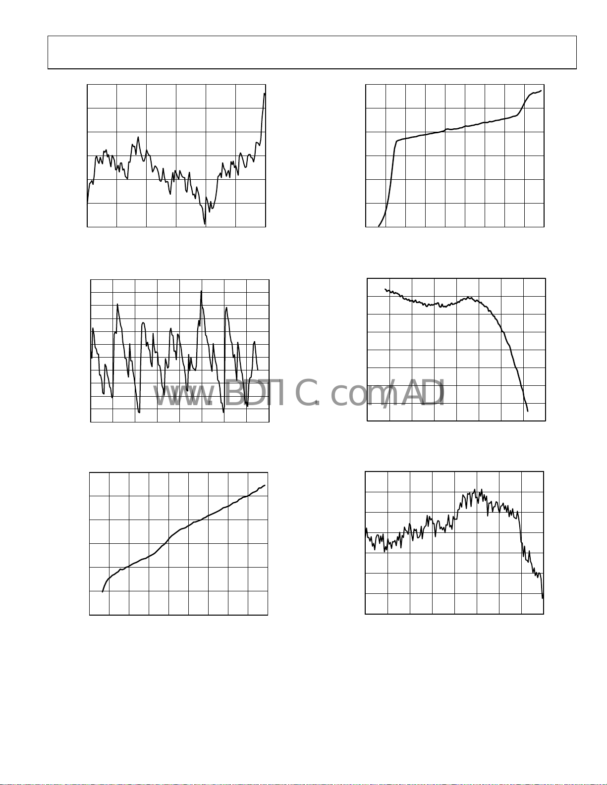
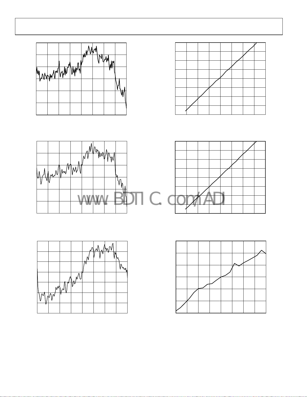
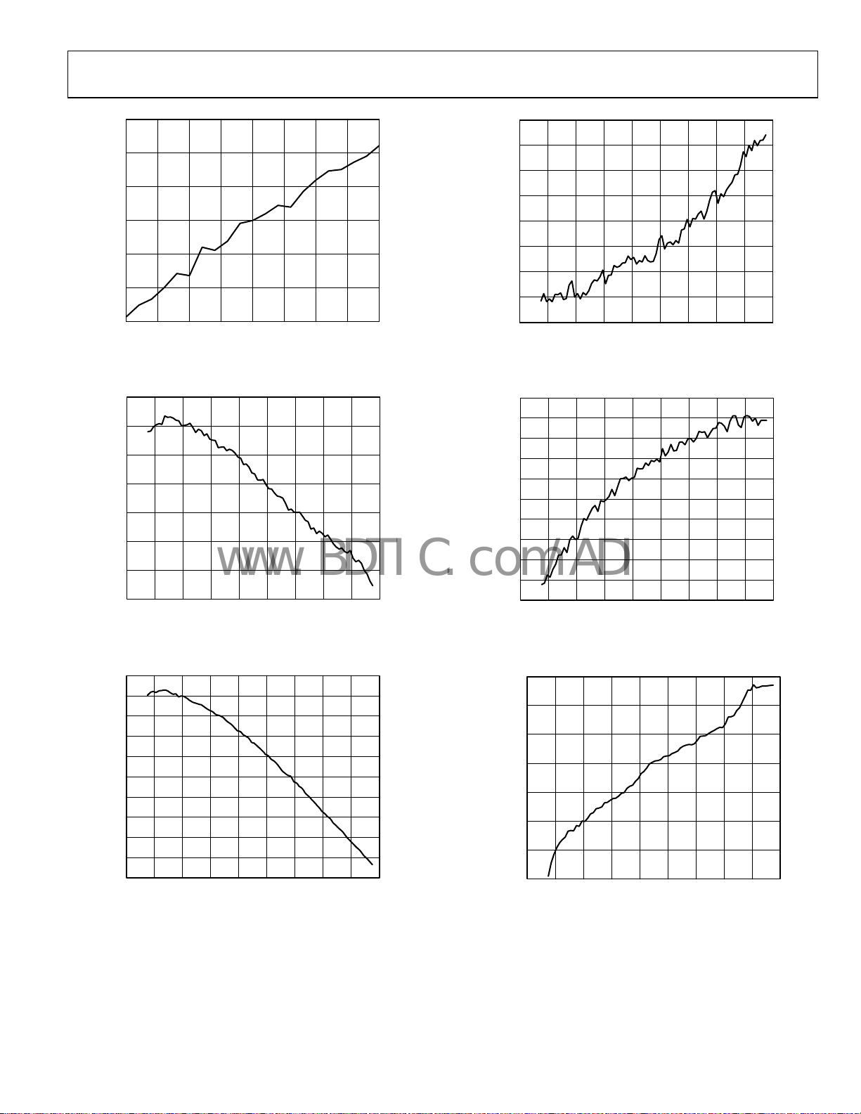
TYPICAL PERFORMANCE CHARACTERISTICS
0.30
0.25
0.20
0.15
0.10
VOLTAGE (V)
0.05
0
–0.05
0 2 4 6 8 10 12 14 18 20
0.5V
0.2V
TIME (ns)
16
07279-003
Figure 3. Driver Small Signal Response; VH = 0.2 V, 0.5 V;
VL = 0.0 V; 50 Ω Termination
1.8
1.6
1.4
1.2
1.0
0.8
0.6
VOLTAGE (V)
0.4
0.2
0
–0.2
020
TIME (ns)
3V
2V
1V
18161412108642
07279-004
Figure 4. Driver Large Signal Response; VH = 1.0 V, 2.0 V, 3.0 V;
VL = 0.0 V; 50 Ω Termination
6
5
4
3
2
VOLTAGE (V)
1
0
5V
3V
1V
1.8
VOLTAGE (V)
–0.2
1.6
1.4
1.2
1.0
0.8
0.6
0.4
0.2
0
TIME (ns)
3V
2V
1V
Figure 6. 50 MHz Driver Response; VH = 1.0 V, 2.0 V, 3.0 V;
VL = 0.0 V, 50 Ω Termination
1.8
3V
2V
1V
VOLTAGE (V)
–0.2
1.6
1.4
1.2
1.0
0.8
0.6
0.4
0.2
0
1
TIME (ns)
Figure 7. 100 MHz Driver Response; VH = 1.0 V, 2.0 V, 3.0 V;
VL = 0.0 V; 50 Ω Termination
1.6
1.4
1.2
1.0
0.8
VOLTAGE (V)
0.6
0.4
0.2
3V
2V
1V
4.5
5.04.03.52.5 3.02.01.51.00.50
07279-006
19 200 23456789101112131415161718
07279-007
–1
020
TIME (ns)
16 181412108642
07279-005
Figure 5. Driver Large Signal Response; VH = 1.0 V, 3.0 V, 5.0 V;
VL = 0.0 V; 500 Ω Termination
Rev. 0 | Page 23 of 52
0
0
TIME (ns)
Figure 8. Response at 200 MH; VH = 1.0 V, 2.0 V, 3.0 V;
VL = 0.0 V; 50 Ω Termination
10987654321
07279-008

ADATE304
www.BDTIC.com/ADI
1.6
1.4
1.2
1.0
0.8
VOLTAGE (V)
0.6
0.4
0.2
0
0312 45 678 109
TIME (ns)
3V
2V
1V
0.5V
Figure 9. 300 MHz Driver Response; VH = 0.5 V, 1.0 V, 2.0 V, 3.0 V;
VL = 0.0 V; 50 Ω Termination
1.0
0.9
0.8
0.7
0.6
0.5
0.4
VOLTAGE (V)
0.3
0.2
0.1
0
0 0.5 1. 0 1.5 2.0 2.5 3.0 3.5 4.0 4.5 5.0
TIME (ns)
2V
1V
0.5V
Figure 10. 400 MHz Driver Response; VH = 0.5 V, 1.0 V, 2.0 V,
VL = 0.0 V; 50 Ω Termination
1.2
1.0
0.8
0.6
VOLTAGE (V)
0.4
0.2
0
200 250 300 350
FREQUENCY (MHz )
Figure 11. Driver Toggle Rate, VH = 2.0 V, VL = 0.0 V, 50 Ω Termination
0.6
0.5
0.4
0.3
0.2
VOLTAGE (V)
0.1
0
–0.1
7279-009
TIME (ns)
19161412108642217151311975310 0
18
07279-012
Figure 12. Driver Active (VH and VL) to and from VTERM Transition;
VH = 1.0 V, VT = 0.5 V, VL = 0.0 V
1.2
1.0
0.8
0.6
0.4
VOLTAGE (V)
0.2
0
–0.2
07279-010
TIME (ns)
19161412108642217151311975310 018
07279-013
Figure 13. Driver Active (VH and VL) to and from VTERM Transition;
VH = 2.0 V, VT = 1.0 V, VL = 0.0 V
1.6
1.4
1.2
1.0
0.8
0.6
VOLTAGE (V)
0.4
0.2
0
–0.2
0
07279-011
TIME (ns)
2018161412108642
07279-014
Figure 14. Driver Active (VH and VL) to and from VTERM Transition;
VH = 3.0 V, VT = 1.5 V, VL = 0.0 V
Rev. 0 | Page 24 of 52

ADATE304
www.BDTIC.com/ADI
20
0.2V NEG
0
20
0
2V POS
–20
–40
TRAILING EDGE ERROR (ps)
–60
–80
12345678
0.2V POS
910
PULSEWIDTH (ns)
Figure 15. Driver Minimum Pulse Width; VH = 0.2 V, VL = 0.0 V
20
0
–20
–40
TRAILING EDGE ERROR (ps)
–60
0.5V NEG
0.5V POS
–20
–40
–60
TRAILING EDGE ERROR ( ps)
–80
–100
12345678
07279-015
2V NEG
PULSEWIDTH (ns)
910
07279-018
Figure 18. Driver Minimum Pulse Width; VH = 2.0 V, VL = 0.0 V
20
0
–20
–40
–60
TRAILING EDGE ERROR (ps)
–80
3V POS
3V NEG
–80
12345678
PULSEWIDTH (ns)
910
Figure 16. Driver Minimum Pulse Width; VH = 0.5 V, VL = 0.0 V
20
1V NEG
0
–20
–40
–60
TRAILING EDGE ERROR (ps)
–80
–100
12345678
1V POS
910
PULSEWIDTH (ns)
Figure 17. Driver Minimum Pulse Width; VH = 1.0 V, VL = 0.0 V
–100
12345678
07279-016
PULSE WI DTH (ns)
910
07279-019
Figure 19. Driver Minimum Pulse Width; VH = 3.0 V, VL = 0.0 V
1.0
0.5
0
–0.5
–1.0
LINEAR ITY E RROR (mV )
–1.5
–2.0
–2 –1 0 1 2 3 4 5 6 7
07279-017
DRIVER OUTPUT VOLTAGE (V)
07279-020
Figure 20. Driver VH Linearity Error
Rev. 0 | Page 25 of 52
ADATE304
www.BDTIC.com/ADI
1.0
120
0.5
0
–0.5
LINEARITY ERROR (mV)
–1.0
–1.5
–2–10123456
DRIVER OUTPUT VOLTAGE (V)
Figure 21. Driver VL Linearity Error
0.8
0.6
0.4
0.2
0
–0.2
–0.4
–0.6
LINEAR ITY E RROR (mV )
–0.8
–1.0
–1.2
–2–101234567
DRIVER OUTPUT VOLTAGE (V)
Figure 22. Driver VT Linearity Error
48.0
47.8
47.6
47.4
47.2
47.0
46.8
46.6
DRIVER OUTPUT RESISTANCE ( )
46.4
46.2
–60 –40 –20 0 20 40 60
DRIVER OUTPUT CURRENT (mA)
Figure 23. Driver Output Resistance vs. Output Current
100
80
60
40
20
DRIVER OUTPUT CURRENT (mA)
0
–20
–2–1012345 76
07279-021
V
DUTx
(V)
07279-024
Figure 24. Driver Output Current Limit; Driver Programmed to −1.25 V;
Swept from −1.25 V to +6.75 V
V
DUTx
20
0
–20
–40
–60
–80
DRIVER OUTPUT CURRENT (mA)
–100
–120
–2–1012345 76
07279-022
V
DUTx
(V)
7279-025
Figure 25. Driver Output Current Limit; Driver Programmed to 6.75 V;
V
Swept from −1.25 V to +6.75 V
DUTx
8
7
6
5
4
3
2
1
0
LINEARITY ERROR (mV)
–1
–2
–3
7279-023
–101 2 3 45 6
VL PROGRAMMED VOLTAGE (V)
07279-026
Figure 26. HVOUT VL Linearity Error
Rev. 0 | Page 26 of 52

ADATE304
www.BDTIC.com/ADI
3
2
1
0
–1
–2
–3
–4
LINEARITY ERROR (mV)
–5
–6
–7
567891011121314
VL PROGRAMMED VOLTAG E (V)
Figure 27. HVOUT VHH Linearity Error
80
70
60
50
40
30
20
10
HVOUT DRIVER CURRENT (mA)
0
–10
–101 2 3 45 6
V
HVOUT
(V)
Figure 28. HVOUT VH Current Limit; VH = −0.1 V;
Swept from −0.1 V to +6.0 V
V
HVOUT
80
60
07279-027
07279-028
1.0
RISE INPUT
0.8
RISE SHMOO
0.6
0.4
VOLTAGE (V)
0.2
0
0 0.6 1.2 1.8 2.4 3.0
FALL INPUT
FALL SHM OO
TIME (ns)
Figure 30. Comparator Shmoo, 1.0 V Input, 0.7 ns (10% to 90%) Input,
50 Ω Terminated
1.0
0.8
0.6
0.4
VOLTAGE (V)
0.2
0
0 0.6 1.2 1.8 2.4 3.0
RISE INPUT
RISE SHM OO
FALL SHM OO
FALL INPUT
TIME (ns)
Figure 31. Comparator Shmoo, 1.5 V Input, 1.0 ns (10% to 90%) Input,
50 Ω Terminated
1.6
RISE INPUT
07279-030
07279-031
40
20
0
–20
–40
HVOUT DRIVER CURRENT (mA)
–60
–80
5 6 7 8 9 101112131415
V
HVOUT
(V)
07279-029
Figure 29. HVOUT VHH Current Limit; VHH = 10.0 V;
V
Swept from −5.9 V to +14.1 V
HVOUT
Rev. 0 | Page 27 of 52
1.2
0.8
VOLTAGE (V)
0.4
0
0 0.6 1.2 1.8 2.4 3.0
FALL INPUT
TIME (ns)
RISE SHMOO
FALL SHM OO
Figure 32. Comparator Shmoo, 1.5 V Input, 1.0 ns (10% to 90%) Input,
50 Ω Terminated
07279-032

ADATE304
–
www.BDTIC.com/ADI
10
0
–10
–20
–30
–40
1V POS
–50
TRAILING EDGE ERROR (ps)
–60
–70
12345678
Figure 33. Comparator Minimum Pulse Width, 1.0 V
1V NEG
PULSEWIDTH (ns)
910
07279-035
0.6
0.4
0.2
0
–0.2
–0.4
–0.6
–0.8
–1.0
LINEARITY ERROR (mV)
–1.2
–1.4
–1.6
–2–101234567
PROGRAMMED THRESHOLD VOLTAGE (V)
Figure 36. Comparator Threshold Linearity
07279-038
100
75
50
25
RISING
0
–25
PROPAGATI ON DELAY VARI ATION (p s)
–50
0.5 1.0 1.5 2.0 2.5
TOTAL
FALL ING
INPUT SLEWRATE (10%-90%) (ns)
Figure 34. Comparator Slew Rate Dispersion, Input Swing = 1.5 V,
Comparator Threshold = 0.75 V
1.8
1.6
1.4
1.2
1.0
0.8
VOLTAGE (V)
0.6
0.4
0.2
0
0 5 10 15 20 25 30 35 40 45 50
TIME (ns)
07279-037
Figure 35. Comparator Output Waveform, COMP_QH0P, COMP_QH0N
2.5
–2.6
–2.7
–2.8
–2.9
–3.0
–3.1
DIFFERENTIAL COMPARAT OR OFFSET (mV)
–3.2
–2 –1 0 1 2 3 4 5
07279-036
INPUT COMMON-MODE VOLTAGE (V)
07279-039
Figure 37. Differential Comparator CMRR
15
10
5
0
–5
LOAD CURRENT (mA)
–10
–15
–2 –1 0 1 2 3 4 5 6
V
DUTx
(V)
07279-040
Figure 38. Active Load Commutation Response; VCOM = 2.0 V;
IOH = IOL = 12 mA
Rev. 0 | Page 28 of 52
ADATE304
www.BDTIC.com/ADI
6
6
4
2
0
–2
LINEARITY ERROR (µA)
–4
–6
024681012
ACTIVE LO AD CURRENT (mA)
Figure 39. Active Load Current Linearity
0.8
0.6
0.4
0.2
0
–0.2
–0.4
–0.6
–0.8
LINEARITY ERROR (mV)
–1.0
–1.2
–1.4
–1 0 1 2 3 4 5 6 7
VCOM VOLTAGE (V)
Figure 40. Active Load VCOM Linearity
5
4
(nA)
3
DUTx
I
2
1
0
–2 –1 0 1 2 3 4 5 76
07279-041
V
DUTx
(V)
07279-044
Figure 42. DUTx Pin Leakage in High-Z Mode
40
20
0
–20
–40
–60
LINEARITY ERROR (µA)
–80
–100
–120
–40 –30 –20 –10 0 10 20 30 40
07279-042
PMU OUTPUT CURRENT (mA)
7279-045
Figure 43. PMU Force Current Range A Linearity
6.0
5.5
5.0
(nA)
4.5
DUTx
I
4.0
3.5
3.0
–2–101234567
V
DUTx
(V)
Figure 41. DUTx Pin Leakage in Low Leakage Mode
07279-043
Rev. 0 | Page 29 of 52
0.8
0.6
0.4
0.2
0
–0.2
LINEARITY ERROR (µA)
–0.4
–0.6
–2.0 –1.5 –1.0 –0.5 0 0.5 1.0 1.5 2.0
PMU OUTPUT CURRENT (mA)
Figure 44. PMU Force Current Range B Linearity
07279-046
ADATE304
www.BDTIC.com/ADI
0.06
0.04
0.02
0
–0.02
LINEARITY ERROR (µA)
–0.04
–0.06
–0.20 –0. 15 –0. 10 –0.05 0 0.05 0. 10 0.15 0. 20
PMU OUTPUT CURRENT (mA)
Figure 45. PMU Force Current Range C Linearity
0.006
0.004
0.002
0
4
3
2
1
0
–1
–2
PMU VOL TAGE ERROR (mV )
–3
–4
–40 –30 –20 –10 0 10 20 30 40
07279-047
I
DUTx
(mA)
7279-050
Figure 48. PMU Force Voltage Range A Output Voltage Error at
6.75 V vs. Output Current
4
3
2
1
0
–0.002
LINEARITY ERROR (µA)
–0.004
–0.006
–0.020 –0.015 –0.010 –0.005 0 0.005 0.010 0.015 0.020
PMU OUTPUT CURRENT (mA)
Figure 46. PMU Force Current Range D Linearity
0.0006
0.0004
0.0002
0
–0.0002
–0.0004
LINEARITY ERROR (µA)
–0.0006
–0.0008
–0.0020 –0.0015 –0.0010 –0. 0050 0 0.0050 0.0010 0. 0015 0.0020
PMU OUTPUT CURRENT (mA)
Figure 47. PMU Force Current Range E Linearity
–1
–2
PMU VOL TAGE ERROR (mV )
–3
–4
7279-048
–40 –30 –20 –10 0 10 20 30 40
I
DUTx
(mA)
7279-051
Figure 49. PMU FV Range A Output Voltage Error at −1.25 V
vs. Output Current
0.6
0.4
0.2
0
–0.2
PMU VOLTAG E ERROR (mV)
–0.4
–0.6
–2.0 –1.5 –1.0 –0.5 0 0.5 1.0 1. 5 2. 0
07279-049
I
DUTx
(mA)
07279-052
Figure 50. PMU FV Range B Output Voltage Error at 6.75 V vs. Output Current
Rev. 0 | Page 30 of 52
ADATE304
www.BDTIC.com/ADI
0.6
0.7
0.4
0.2
0
–0.2
PMU VOL TAGE ERROR (mV )
–0.4
–0.6
–2.0 –1.5 –1.0 –0.5 0 0.5 1.0 1. 5 2.0
I
DUTx
(mA)
Figure 51. PMU FV Range B Output Voltage Error at −1.25 V
vs. Output Current
5
0
–5
–10
–15
–20
PMU CURRENT ERROR (µA)
–25
–30
–2–1012345 76
V
DUTx
(V)
Figure 52. PMU FI Range A Output Current Error at −32 mA vs. Output
Voltage; Output Voltage Is Pulled Externally
10
0
–10
–20
–30
–40
–50
–60
PMU CURRENT ERROR (µA)
–70
–80
–90
–2–101234567
V
DUTx
(V)
Figure 53. PMU FI Range A Output Current Error at +32 mA vs. Output
Voltage; Output Voltage Is Pulled Externally
0.6
0.5
0.4
0.3
0.2
0.1
PMU CURRENT ERROR (µA)
0
–0.1
7279-053
–2 –1 0 1 2 3 4 5 6 7
V
DUTx
(V)
07279-056
Figure 54. PMU FI Range B Output Current Error at −2 mA vs. Output Voltage;
Output Voltage Is Pulled Externally
0.7
0.6
0.5
0.4
0.3
0.2
0.1
0
PMU CURRENT ERROR (µA)
–0.1
–0.2
–0.3
–2 –1 0 1 2 3 4 5 6 7
07279-054
V
DUTx
(V)
07279-057
Figure 55. PMU FI Range B Output Current Error at +2 mA vs. Output Voltage;
Output Voltage Is Pulled Externally
0.0025
0.0020
0.0015
0.0010
0.0005
0
PMU CURRENT ERROR (µA)
–0.0005
–0.0010
–2–101234567
07279-055
V
DUTx
(V)
07279-058
Figure 56. PMU FI Range E Output Current Error at −2 μA vs. Output Voltage;
Output Voltage Is Pulled Externally
Rev. 0 | Page 31 of 52

ADATE304
www.BDTIC.com/ADI
0.0020
0.0015
0.0010
0.0005
PMU CURRENT ERROR (µA)
0
–0.0005
–2–1012345 76
V
DUTx
(V)
07279-059
Figure 57. PMU FI Range E Output Current Error at +2 μA vs. Output Voltage;
Output Voltage Is Pulled Externally
0.5
0.4
0.3
0.2
0.1
PMU VOLTAG E ERROR (mV)
0
–0.1
–2 –1 0 1 2 3 4 5
V
DUTx
(V)
07279-060
Figure 58. PMU Measure Current Range B CMRR,
Externally Pulling 1 mA, FVMI
C1
(100mV/DIV)
(500ps/DI V)
Figure 60. Eye Diagram, 400 Mbps, PRBS31; VH = 1.0 V, VL = 0.0 V
C1
(100mV/DIV )
(200ps/DI V)
Figure 61. Eye Diagram, 600 Mbps, PRBS31; VH = 1.0 V, VL = 0.0 V
07279-062
07279-063
C1
(100mV/DIV)
(1ns/DIV)
07279-061
Figure 59. Eye Diagram, 200 Mbps, PRBS31; VH = 1.0 V, VL = 0.0 V
Rev. 0 | Page 32 of 52
C1
(200mV/DIV)
(500ps/DIV )
Figure 62. Eye Diagram, 400 Mbps, PRBS31; VH = 2.0 V, VL = 0.0 V
07279-065
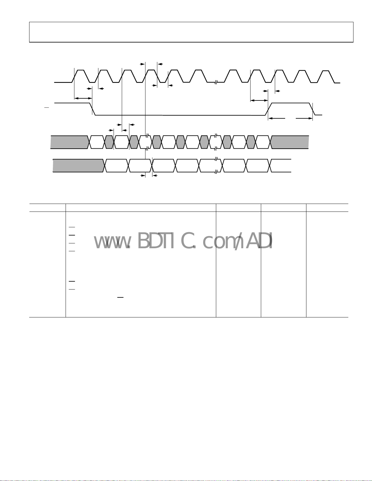
ADATE304
www.BDTIC.com/ADI
SPI DETAILS
t
CH
SCLK
t
CL
t
CSHD
t
CSSD
t
CSW
CS
t
CSHA
t
CSSA
t
t
DS
DH
SDIN
SDOUT
DO_15
DATA[14]DATA[15]
LAST
DO_14
LAST
CH[1] R/ W
DO_13
LAST
t
DO
DO_12
LAST
ADDR[1] ADDR[0]
DO_2
LAST
DO_1
LAST
DO_0
LAST
Figure 63. SPI Timing Diagram
Table 17. Serial Peripheral Interface Timing Requirements
Symbol Parameter Min Max Unit
tCH SCLK minimum high 9.0 ns
tCL SCLK minimum low 9.0 ns
t
CSHA
t
CSSA
t
CSHD
t
CSSD
SDIN hold 3.0 ns
t
DH
t
SDIN setup 3.0 ns
DS
t
SDOUT data out 15.0 ns
DO
t
CSW
t
CSTP
assert hold
CS
assert setup
CS
deassert hold
CS
deassert setup
CS
1
minimum between assertions
CS
minimum directly after a read request
CS
Minimum delay after CS
stopped (not shown in ); this allows any internal
is deasserted before SCLK can be
Figure 63
3.0
3.0
3.0
3.0
ns
ns
ns
ns
2 SCLK cycles
3
SCLK cycles
16 SCLK cycles
operations to complete
1
An extra cycle is needed after a read request to prime the read data into the SPI shift register.
7279-067
Rev. 0 | Page 33 of 52
ADATE304
9
www.BDTIC.com/ADI
DEFINITION OF SPI WORD
The SPI can accept variable length words, depending on the
operation. At most, the word length equals 24 bits: 16 bits of
data, two channel selects, one read/write (R/W) selector, and a
5-bit address.
Depending on the operation, the data can be smaller or, in the
case of a read operation, nonexistent.
Example 1: 16-Bit Write
Write 16 bits of data to a register or DAC; ignore unused MSBs. For example, Bit 15 and Bit 14 are ignored, and Bit 13 through Bit 0 are
applied to the 14-bit DAC.
Table 18. Channel Selection
Channel 1 Channel 0 Channel Selected
0 0
NOP (no channel selected, no register
changes)
0 1 Channel 0 selected
1 0
Channel 1 selected
1 1 Channel 0 and Channel 1 selected
Table 19. R/W Definition
R/W Description
0
Current register specified by address shifts out of
SDOUT on next shift operation
1
Current data written to the register specified by
address and channel select
DATA[15:0] CH[1:0] R/W ADDR[4:0]
Figure 64. 16-Bit Write
07279-068
Example 2: 14-Bit Write
Write 14 bits of data to the DAC.
DATA[13:0] CH[1:0] R/ W ADDR[4:0]
Figure 65. 14-Bit Write
-06
07279
Example 3a: 2-Bit Write
Write two bits of data to the 2-bit register.
DATA[1:0] CH[1:0] R/W ADDR[4:0]
Figure 66. 2-Bit Write
07279-070
Example 3b: 2-Bit Write
Write two bits of data to the 2-bit register. Bit 15 through Bit 2 are ignored and Bit 1 through Bit 0 are applied to the register.
DATA[15:0] CH[1:0] R/W ADDR[4:0]
Figure 67. 2-Bit Write
07279-071
Example 4: Read Request
Read request and follow with a second instruction (could be NOP) to clock out the data.
DATA[15:0] CH[1:0] R/W ADDR[4:0]
Figure 68. Read Request
Rev. 0 | Page 34 of 52
CH[1:0] R/W = 0 ADDR[4:0]
07279-072
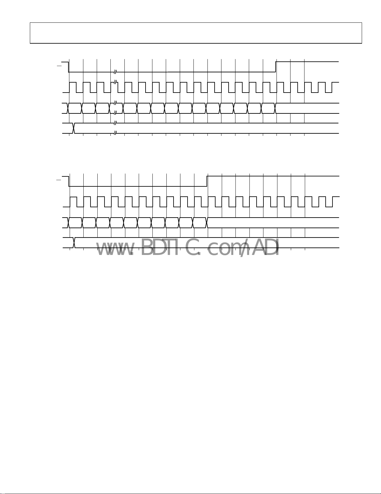
ADATE304
www.BDTIC.com/ADI
WRITE OPERATION
CS
INPUT
SCLK
INPUT
INPUT
SDOUT
OUTPUT
NOTES
1. R/W = 1.
2. X = DON’T CARE.
INPUT
INPUT
INPUT
SDOUT
OUTPUT
NOTES
1. R/W = 1.
2. X = DON’T CARE.
SDIN
CS
SCLK
SDIN
DATA[14]DATA[15] DATA[13]
0 232221201918171615141312 24 25
DATA[2] DATA[1] DATA[0] C H[1 ] CH[ 0]
R/W
ADDR[3] ADDR[1]ADDR[4] ADDR[2] ADDR[0]
X
Figure 69. 16-Bit SPI Write
DATA[1] DATA[0] CH [1] CH[ 0] ADDR[4] ADDR[3] ADDR[ 2] ADDR[1 ] ADDR[0]R/W
0 1110987654123
X
X
Figure 70. 2-Bit SPI Write
X
07279-073
07279-074
Rev. 0 | Page 35 of 52

ADATE304
www.BDTIC.com/ADI
READ OPERATION
The read operation is a two-stage operation. First, a word is
CS
shifted in, specifying which register to read.
for three clock cycles, and then a second word is shifted in to
obtain the readback data. This second word can be either
another operation or an NOP address. If another operation is
shifted in, it must shift in at least eight bits of data to read back
CS
INPUT
SCLK
INPUT
is deasserted
the previous specified data. The NOP address can be used for
this read if there is no need to read/write another register. To
maintain the clarity of the operation, it is strongly recommended
that the NOP address be used for all reads.
Any register read that is fewer than 16 bits has zeros filled in the
top bits to make it a 16-bit word.
SDIN
INPUT
SDOUT
OUTPUT
NOTES
1. X = DON’T CARE.
INPUT
SCLK
INPUT
SDIN
INPUT
SDOUT
OUTPUT
NOTES
1. X = DON’T CARE.
INPUT
CS
CS
DATA[15:0], VALUE IS A DON’ T CARE
0 2524232221201918171615141312
X READ DATA X
Figure 71. SPI Read Overview
CH[1]
X
ADDR[4] ADDR[3] ADDR[2] A DDR[1] ADDR[0]
R/WCH[ 0]
X
Figure 72. SPI Read—Details of Read Request
XXREAD INSTRUCTI ON NOP
7279-075
07279-076
SCLK
INPUT
SDIN
INPUT
SDOUT
OUTPUT
NOTES
1. RDATA IS T HE REGIST ER VALUE BEING READ.
2. X = DON’T CARE.
DATA[15:0], VALUE IS A DON’ T CARE
0 2524232221201918171615141312
RDATA[2] RDATA[1]RDATA[15] RDATA[14] RDATA[0]
CH[1]
CH[0]
Figure 73. SPI Read—Details of Read Out
Rev. 0 | Page 36 of 52
R/W = 1
ADDR[4:0] = 0x00 (NOP )
X
X
07279-077

ADATE304
www.BDTIC.com/ADI
RESET OPERATION
The ADATE304 contains an asynchronous reset feature. The
ADATE304 can be reset to the default values shown in Tab l e 2 0
100ns
RST
CS
SCLK
MINIMUM OF TWO SCLK EDGES AFTER ASSERTI NG RST BEFO RE RESUMING NO RMAL OPERAT ION.
MINIMUM
Figure 74. Reset Operation
by utilizing the
RST
the
for a minimum of two SCLK cycles.
RST
pin. To initiate the reset operation, deassert
pin for a minimum of 100 ns and deassert the CS pin
07279-078
Rev. 0 | Page 37 of 52

ADATE304
www.BDTIC.com/ADI
REGISTER MAP
The ADDR[4:0] bits determine the destination register of the data being written to the ADATE304.
Table 20. Register Selection
DATA[15:0] CH[1:0] R/W ADDR[4:0] Register Selected Reset State
1
N/A
DATA[13:0] CH[1:0] R/W 0x01 VH DAC level 4096d
DATA[13:0] CH[1:0] R/W 0x02 VL DAC level 4096d
DATA[13:0] CH[1:0] R/W 0x03 VT/VCOM DAC level 4096d
DATA[13:0] CH[1:0] R/W 0x04 VOL DAC level 4096d
DATA[13:0] CH[1:0] R/W 0x05 VOH DAC level 4096d
DATA[13:0] CH[1:0] R/W 0x06 VCH DAC level 4096d
DATA[13:0] CH[1:0] R/W 0x07 VCL DAC level 4096d
DATA[13:0] CH[1:0] R/W 0x08 V(IOH ) DAC level 4096d
DATA[13:0] CH[1:0] R/W 0x09 V(IOL ) DAC level 4096d
DATA[13:0] CH[1] R/W 0x0A OVD high level 4096d
DATA[13:0] CH[0] R/W 0x0A OVD low level 4096d
DATA[15:0] CH[1:0] R/W 0x0B PMUDAC level 16384d
DATA[2:0] CH[1:0] R/W 0x0C PE/PMU enable 000b
DATA[2:0] CH[1:0] R/W 0x0D Channel state 000b
DATA[9:0] CH[1:0] R/W 0x0E PMU state 0d
DATA[2:0] CH[1:0] R/W 0x0F PMU measure enable 000b
DATA[0] CH[1:0] R/W 0x10 Differential comparator enable 0b
DATA[1:0] CH[1:0] R/W 0x11 16-bit DAC monitor 00b
DATA[1:0] CH[1:0] R/W 0x12 OVD_CHx alarm mask 01b
DATA[2:0] CH[1:0] R 0x13 OVD_CHx alarm state N/A
N/A N/A N/A 0x14 to 0x1F Reserved N/A
1
N/A means not applicable.
N/A N/A 0x00 NOP N/A
Rev. 0 | Page 38 of 52

ADATE304
www.BDTIC.com/ADI
DETAILS OF REGISTERS
Table 21. PE/PMU Enable (ADDR[4:0] = 0x0C)
Bit Name Description
DATA[2] PMU enable 0 = disable PMU force output and clamps, place PMU in MV mode
1 = enable PMU force output
When set to 0, the PMU state bits are ignored, except for the PMU sense path (DATA[7])
DATA[1] Force VT 0 = normal driver operation
1 = force driver to VT
See Table 29 for complete functionality of this bit
DATA[0] PE disable 0 = enable driver functions
1 = disable driver (low leakage)
See Table 29 for complete functionality of this bit
Table 22. Channel State (ADDR[4:0] = 0x0D)
Bit Name Description
DATA[2] HV mode select 0 = HV driver in low impedance.
1 = enable HV driver.
This bit affects Channel 0 only. Ensure that the Channel 0 bit in SPI write is active.
Channel 1 bit in SPI write is don’t care.
DATA[1] Load enable 0 = disable load.
1 = enable load.
See Tab le 29 for complete functionality of this bit.
DATA[0] Driver high-Z or VT 0 = enable Driver high-Z function.
1 = enable Driver VTERM function.
See Tab le 29 for complete functionality of this bit.
Table 23. PMU State (ADDR[4:0] = 0x0E)
Bit Name Description
DATA[9:8] PMU input selection 00 = V
01 = 2.5 V + V
1X = PMUDAC
DATA[7] PMU sense path 0 = internal sense
1 = external sense
DATA[6] Reserved
DATA[5] PMU clamp enable 0 = disable clamps
1 = enable clamps
DATA[4] PMU measure voltage or current 0 = measure voltage mode
1 = measure current mode
DATA[3] PMU force voltage or current 0 = force voltage mode
1 = force current mode
DATA[2:0] PMU range 0XX = 2 A range
100 = 20 A range
101 = 200 A range
110 = 2 mA range
111 = 32 mA range
1
Note that when ADDR[4:0] = 0x0C, the PMU enable bit (DATA[2]) = 0, PMU force outputs and clamps are disabled, and the PMU is placed into measure voltage mode.
PMU State DATA[9:8] and DATA[6:0] are ignored, and only the DATA[7] PMU sense path is valid.
2
X means don’t care.
1, 2
(calibrated for 0.0 V voltage reference)
DUTGND
(calibrated for 0.0 A current reference)
DUTGND
Rev. 0 | Page 39 of 52
ADATE304
www.BDTIC.com/ADI
Table 24. PMU Measure Enable (ADDR[4:0] = 0x0F)1
Bit Name Description
DATA[2:1] MEASOUT01 select 00 = PMU MEASOUT Channel 0
01 = PMU MEASOUT Channel 1
10 = Temperature sensor ground reference
11 = Temperature sensor
DATA[0] MEASOUT01 output enable
1
This register is written to or read from when either of the CH[1:0] bits is 1.
Table 25. Differential Comparator Enable (ADDR[4:0] = 0x10)1
Bit Name Description
DATA[0] Differential Comparator Enable
1
This register is written to or read from when either of the CH[1:0] bits is 1.
Table 26. DAC16_MON (16-Bit DAC Monitor) (ADDR[4:0] = 0x11)1
Bit Name Description
DATA[1] 16-Bit DAC mux enable 0 = 16-bit DAC mux is tristated
1 = 16-bit DAC mux is enabled
DATA[0] 16-Bit DAC mux select 0 = 16-bit DAC Channel 0
1 = 16-bit DAC Channel 1
1
This register is written to or read from when either of the CH[1:0] bits is 1.
0 = MEASOUT01 is tristated
1 = MEASOUT01 is enabled
0 = differential comparator is disabled; the Channel 0 normal window
comparator (NWC) outputs are located on Channel 0
1 = differential comparator is enabled; the differential comparator outputs
are located on Channel 0
Table 27. OVD_CHx Alarm Mask (ADDR[4:0] = 0x12)
Bit Name Description
DATA[1] PMU mask 0 = disable PMU alarm flag
1 = enable PMU alarm flag
DATA[0] OVD mask 0 = disable OVD alarm flag
1 = enable OVD alarm flag
Table 28. OVD_CHx Alarm State (ADDR[4:0] = 0x13)1
Bit Name Description
DATA[2] PMU clamp flag 0 = PMU is not clamped
1 = PMU is clamped
DATA[1] OVD high flag 0 = DUT voltage < OVD high voltage
1 = DUT voltage > OVD high voltage
DATA[0] OVD low flag 0 = DUT voltage > OVD low voltage
1 = DUT voltage < OVD low voltage
1
This register is a read-only register.
Rev. 0 | Page 40 of 52

ADATE304
www.BDTIC.com/ADI
USER INFORMATION
POWER SUPPLY CONSIDERATIONS
Power Supply Sequencing
It is recommended that the power supplies be brought up in the
following order:
1. Grounds (DGND, AGND, VREF_GND)
2. V
3. V
4. V
5. V
If the HVOUT pin is not used, the V
connected to V
SS
CC
DD
PLUS
, V
COMP_VTT
DD
, and V
.
REF
supply can be
PLUS
TRUTH TABLES
Table 29. Driver and Load Truth Table1
Registers Signals
PE Disable
DATA[0]
ADDR[4:0] = 0x0C
1 X X X X X High-Z without clamps Power-down
0 1 X X X X VT Power-down
0 0 0 0 0 0 VL Power-down
0 0 0 0 0 1 High-Z with clamps Power-down
0 0 0 0 1 0 VH Power-down
0 0 0 0 1 1 High-Z with clamps Power-down
0 0 0 1 0 0 VL Power-down
0 0 0 1 0 1 VT Power-down
0 0 0 1 1 0 VH Power-down
0 0 0 1 1 1 VT Power-down
0 0 1 0 0 0 VL Active off
0 0 1 0 0 1 High-Z with clamps Active on
0 0 1 0 1 0 VH Active off
0 0 1 0 1 1 High-Z with clamps Active on
0 0 1 1 0 0 VL Active on
0 0 1 1 0 1 High-Z with clamps Active on
0 0 1 1 1 0 VH Active on
0 0 1 1 1 1 High-Z with clamps Active on
1
X means don’t care.
Table 30. HVOUT Truth Table1
HVOUT Mode Select
DATA[2]
ADDR[4:0] =0x0D
1 1 X VHH mode; VHH = (VT + 1 V) × 2 + DUTGND (Channel 0 VT DAC)
1 0 0 VL (Channel 0 VL DAC)
1 0 1 VH (Channel 0 VH DAC)
0 X X Disabled (HVOUT pin set to 0 V low impedance)
1
X means don’t care.
Force VT
DATA[1]
ADDR[4:0] = 0x0C
Channel 0
RCV
Load Enable
DATA[1]
ADDR[4:0] = 0x0D
Channel 0
DATA
Driver High-Z/VT
DATA[0]
ADDR[4:0] = 0x0D
Power Supply Decoupling
The ADATE304 is a high performance device that requires
close attention to power supply decoupling to deliver the best
performance. The use of full power planes with low inductance
capacitors placed as close to the power pins as possible is recommended. The following power connections are the most important:
• VPLUS to AGND (for the HVOUT driver)
• VDD to VSS near the DUTx pin (for the driver)
• VDD and VSS to AGND near the DUTx pin (for the
comparators)
• VCC to DGND (for the digital)
Additionally, large bulk capacitors (that is, 10 μF) should be
used on every power supply on the printed circuit board (PCB).
DATAx RCVx
HVOUT Driver Output
Driver State Load State
Rev. 0 | Page 41 of 52
ADATE304
www.BDTIC.com/ADI
Table 31. Comparator Truth Table
Differential
Comparator Enable
DATA[0]
ADDR[4:0] = 0x10 COMP_QH0 COMP_QL0 COMP_QH1 COMP_QL1
0 Normal window mode Normal window mode Normal window mode Normal window mode
Logic high: VOH0 < V
Logic low: VOH0 > V
1 Differential comparator mode Differential comparator mode Normal window mode Normal window mode
Logic high: VOH0 < V
Logic low: VOH0 > V
Logic high: VOL0 < V
DUT0
Logic low: VOL0 > V
DUT0
− V
DUT0
DUT0
Logic high: VOL0 < V
DUT1
− V
Logic low: VOL0 > V
DUT1
Logic high: VOH1 < V
DUT0
Logic low: VOH1 > V
DUT0
− V
DUT0
DUT0
Logic high: VOH1 < V
DUT1
− V
Logic low: VOH1 > V
DUT1
Logic high: VOL1 < V
DUT1
Logic low: VOL1 > V
DUT1
Logic high: VOL1 < V
DUT1
Logic low: VOL1 > V
DUT1
DUT1
DUT1
DUT1
DUT1
Rev. 0 | Page 42 of 52

ADATE304
www.BDTIC.com/ADI
DETAILS OF DACS vs. LEVELS
There are ten 14-bit DACs per channel. These DACs provide
levels for the driver, comparator, load currents, VHH buffer, OVD,
and clamp levels. There are three versions of output levels as
follows:
• −2.5 V to +7.5 V and tracks DUTGND. Controls the VH,
VL, VT/VCOM/VHH, VOH, VOL, VCH, and VCL levels.
Table 32. Level Transfer Functions
DAC Transfer Function
V
= 2.0 × (V
OUT
Code = [V
V
= 4.0 × (V
OUT
Code = [V
V
= 2.0 × (V
OUT
Code = [V
I
= [2.0 × (V
OUT
Code = [(I
V
= 2.0 × (V
OUT
Code = [V
I
= [2.0 × (V
OUT
Code = [(I
I
= [2.0 × (V
OUT
Code = [(I
I
= [2.0 × (V
OUT
Code = [(I
I
= [2.0 × (V
OUT
Code = [(I
I
= [2.0 × (V
OUT
Code = [(I
1
Programmable range includes a margin outside the specified part performance, allowing for offset/gain calibration.
− V
REF
− V
OUT
DUTGND
− V
REF
− V
OUT
DUTGND
− V
REF
− V
OUT
DUTGND
− V
REF
× (5.0/0.012)) + 0.5 × (V
OUT
− V
REF
− V
OUT
DUTGND
− V
REF
× (5.0/0.050)) + 2.5 + 0.5 × (V
OUT
− V
REF
× (5.0/0.004)) + 2.5 + 0.5 × (V
OUT
− V
REF
× (5.0/0.0004)) + 2.5 + 0.5 × (V
OUT
− V
REF
× (5.0/0.00004)) + 2.5 + 0.5 × (V
OUT
− V
REF
× (5.0/0.000004)) + 2.5 + 0.5 × (V
OUT
) × (Code/(214)) − 0.5 × (V
REF_GND
+ 0.5 × (V
REF_GND
− V
REF
) × (Code/(214)) − 1.0 × (V
− 2.0 + 1.0 × (V
) × (Code/(214)) − 0.6 × (V
REF_GND
+ 0.6 × (V
REF_GND
REF_GND
+ 0.5 × (V
REF_GND
REF_GND
REF_GND
REF_GND
REF_GND
− V
REF
) × (Code/(214)) − 0.5 × (V
REF
) × (Code/(216)) − 0.5 × (V
− V
REF
) × (Code/(216)) − 0.5 × (V
) × (Code/(216)) − 0.5 × (V
) × (Code/(216)) − 0.5 × (V
) × (Code/(216)) − 0.5 × (V
) × (Code/(216)) − 0.5 × (V
REF_GND
REF
REF_GND
REF_GND
)] × [(214)/(2.0 × (V
− V
)] × [(214)/(4.0 × (V
REF_GND
)] × [(214)/(2.0 × (V
− V
)] × [(214)/(2.0 × (V
REF_GND
)] × [(216)/(2.0 × (V
− V
REF
REF_GND
− V
REF
REF_GND
− V
REF
REF_GND
− V
REF
− V
REF
REF
REF
REF
REF
REF
REF
− V
− V
− V
− V
− V
− V
) + V
REF_GND
REF
) + 2.0 + V
REF_GND
) + V
REF_GND
REF
)] × (0.012/5.0)
REF_GND
) + V
REF_GND
REF
) − 2.5] × (0.050/5.0)
REF_GND
)] × [(216)/(2.0 × (V
REF
− V
) − 2.5] × (0.004/5.0)
REF_GND
)] × [(216)/(2.0 × (V
REF
− V
) − 2.5] × (0.0004/5.0)
REF_GND
)] × [(216)/(2.0 × (V
− V
REF
REF_GND
− V
REF
REF_GND
) − 2.5] × (0.00004/5.0)
REF_GND
)] × [(216)/(2.0 × (V
) − 2.5] × (0.000004/5.0)
REF_GND
)] × [(216)/(2.0 × (V
− V
− V
− V
DUTGND
REF_GND
REF
DUTGND
REF_GND
REF
DUTGND
REF_GND
• −3.0 V to +7.0 V and tracks DUTGND. Controls the
OVD levels.
• −2.5 V to +7.5 V and does not track DUTGND. Controls
the IOH and IOL levels.
There is one 16-bit DAC per channel. This DAC provides the
levels for the PMU. The output level is as follows:
• −2.5 V to +7.5 V and tracks DUTGND; controls the
PMU levels.
1
Levels
VH, VL, VT/VCOM,
VOL, VOH, VCH, VCL
− V
))]
DUTGND
REF_GND
Programmable Range
(All 0s to All 1s)
−2.5 V to +7.5 V
−3.0 V to +17.0 V VHH
))]
−3.0 V to +7.0 V OVD
))]
−6 mA to +18 mA IOH, IOL
− V
REF_GND
))]
−2.5 V to +7.5 V PMUDAC
))]
REF
REF
− V
− V
REF
REF
REF
− V
− V
− V
REF_GND
REF_GND
REF_GND
REF_GND
REF_GND
−50 mA to +50 mA
))]
−4 mA to +4 mA
))]
−400 A to +400 A
))]
−40 A to +40 A
))]
−4 A to +4 A
))]
PMUDAC
(PMU FI Range A)
PMUDAC
(PMU FI Range B)
PMUDAC
(PMU FI Range C)
PMUDAC
(PMU FI Range D)
PMUDAC
(PMU FI Range E)
Table 33. Load Transfer Functions
Load Level Transfer Function
1
IOL V(IOL)/5 V × 12 mA
IOH V(IOH)/5 V × 12 mA
1
V(IOH)and V(IOL) DAC levels are not referenced to DUTGND.
Table 34. PMU Transfer Functions
PMU Mode Transfer Functions
Force Voltage V
Measure Voltage V
Force Current I
Measure Current V
1
R = 15.5 Ω for Range A; 250 Ω for Range B; 2.5 kΩ for Range C; 25 kΩ for Range D; 250 kΩ for Range E.
= PMUDAC
OUT
= V
MEASOUT01
= [PMUDAC − (V
OUT
= (V
MEASOUT01
(internal sense) or V
DUTx
/2)]/(R1 × 5)
REF
/2) + V
REF
DUTGND
Table 35. PMU User Required Capacitors
Capacitor Location
220 pF Across Pin C10 (FFCAP_0B) and Pin E10 (FFCAP_0A)
220 pF Across Pin C1 (FFCAP _1B) and Pin E1 (FFCAP_1A)
330 pF Between GND and Pin B9 (SCAP0)
330 pF Between GND and Pin B2 (SCAP1)
Rev. 0 | Page 43 of 52
+ (I
× 5 × R1)
DUTx
MEASOUT01
= V
(external sense)
PMUS_CHx

ADATE304
www.BDTIC.com/ADI
Table 36. Temperature Sensor
Temperature Output
0 K 0 V
300 K 3 V
x K (x K) × 10 mV/K
Table 37. Power Supply Ranges
Parameter Range 1 Range 2
Nominal VDD +10.75 V +10.0 V
Nominal VSS −5.00 V −5.75 V
Driver
VH range −1.15 V to +6.75 V −1.9 V to +6.0 V
VL range −1.25 V to +6.65 V −2.0 V to +5.9 V
VT range −1.25 V to +6.75 V −2.0 V to +6.0 V
Functional Amplitude 8.0 V 8.0 V
Reflection Clamp
VCH Range −1.0 V to +6.75 V −1.0 V to +6.0 V
VCL Range −1.25 V to +5.75 V −2.0 V to +5.0 V
Comparator Input Voltage Range −1.25 V to +6.75 V −2.0 V to +6.0 V
Active Load VCOM Range −1.00 V to +6.50 V −1.75 V to +5.75 V
PMU
Force Voltage Range −1.25 V to +6.75 V −2.0 V to +6.0 V
Measure Voltage Range −1.25 V to +6.75 V −2.0 V to +6.0 V
Force Current Voltage Range −1.25 V to +6.75 V −2.0 V to +6.0 V
Measure Current Voltage Range −1.25 V to +6.75 V −2.0 V to +6.0 V
Low Clamp Range −1.25 V to +4.75 V −2.0 V to +4.0 V
High Clamp Range 0.75 V to 6.75 V 0.0 V to 6.0 V
OVD −2.25 V to +7.0 V −3.0 V to +7.0 V
Table 38. Default Test Conditions (Range 1)
Name Default Test Condition
VH DAC Level +2.0 V
VL DAC Level +0.0 V
VT/VCOM DAC Level +1.0 V
VOL DAC Level −1.0 V
VOH DAC Level +6.0 V
VCH DAC Level +7.5 V
VCL DAC Level −2.5 V
IOH DAC Level 0.0 A
IOL DAC Level 0.0 A
OVD Low DAC Level −2.5 V
OVD High DAC Level +6.5 V
PMUDAC DAC Level 0.0 V
PE/PMU Enable 0x0000: PMU disabled, VT not forced through driver, PE enabled
Channel State 0x0000: HV mode disabled, load disabled, VTERM inactive
PMU State 0x0000: input of DUTGND, internal sense, clamps disabled, FVMV, Range E
PMU Measure Enable 0x0000: MEASOUT01 pin tristated
Differential Comparator Enable 0x0000: normal window comparator mode
16-Bit DAC Monitor 0x0000: DAC16_MON tristated
OVD_CHx Alarm Mask 0x0000: disable alarm functions
Data Input Logic low
Receive Input Logic low
DUTx Pin Unterminated
Comparator Output Unterminated
Rev. 0 | Page 44 of 52

ADATE304
www.BDTIC.com/ADI
RECOMMENDED PMU MODE SWITCHING SEQUENCES
To minimize any possible aberrations and voltage spikes on the
DUT output, specific mode switching sequences are recommended
for the following transitions:
• PMU disable to PMU enable.
• PMU force voltage mode to PMU force current mode.
• PMU force current mode to PMU force voltage mode.
PMU Disable to PMU Enable
Note that, in Ta b le 3 9 through Tabl e 4 9 , X indicates the don’t
care bit.
Step 1. Ta b le 3 9 lists the state of the registers in PMU disabled
mode.
Table 39.
Register Bits Setting
PE/PMU Enable
Register, ADDR[4:0]
= 0x0C
PMU State
Register, ADDR[4:0]
= 0x0E
Step 2. Write to Register ADDR[4:0] = 0x0E (see Tabl e 40).
Table 40.
Register Bits Setting Comments
PMU State
Register,
ADDR[4:0] =
0x0E
Step 3. Write to Register ADDR[4:0] = 0x0C (see Tab l e 41 ).
Table 41.
Register Bits Setting Comments
PE/PMU Enable
Register,
ADDR[4:0] = 0x0C
DATA[2] 0
DATA[9:8] XX
DATA[7] X
DATA[6] X
DATA[5] X
DATA[4] X
DATA[3] X
DATA[2:0] XXX
DATA[9:8]
DATA[7] X
DATA[6] X
DATA[5] X
DATA[4] X
DATA[3] 0
DATA[2:0] XXX Set desired range
DATA[2] 1
1X or
00
Set desired input
selection
This bit must be set
to force voltage mode
to reduce aberrations
PMU is now enabled
in force voltage
mode
PMU Force Voltage Mode to PMU Force Current Mode
Step 1. Ta b le 4 2 lists the state of registers in force voltage mode.
Table 42.
Register Bits Setting
PE/PMU Enable
Register, ADDR[4:0]
= 0x0C
PMU State Register,
ADDR[4:0] = 0x0E
DATA[2] 1
DATA[9:8] XX
DATA[7] X
DATA[6] X
DATA[5] X
DATA[4] X
DATA[3] 0
DATA[2:0] XXX
Step 2. Write to Register ADDR[4:0] = 0x0E (see Ta b l e 4 3 ).
Table 43.
Register Bits Setting Comments
PMU State Register,
ADDR[4:0] = 0x0E
DATA[9:8] 01
DATA[7] X
DATA[6] X
DATA[5] X
DATA[4] X
DATA[3] 1
DATA[2:0] 0XX
Set 2.5 V +
DUTGND input
selection
Set to force
current mode
The 2 A range
has the
minimum offset
current
Step 3. Write to Register ADDR[4:0] = 0x0B (see Ta b l e 4 4 ).
Table 44.
Register Bits Setting Comments
VIN 16-Bit DAC,
ADDR[4:0] = 0x0B
DATA[15:0] X
Update the VIN
16-Bit DAC
register to the
desired value
Step 4. Write to Register ADDR[4:0] = 0x0E (see Ta b l e 4 5 ).
Table 45.
Register Bits Setting Comments
PMU State Register,
ADDR[4:0] = 0x0E
DATA[9:8] 1X
DATA[7] X
DATA[6] X
DATA[5] X
DATA[4] X
DATA[3] 1
DATA[2:0] XXX
Set VIN input
selection
Set to the
desired current
range
Rev. 0 | Page 45 of 52
ADATE304
www.BDTIC.com/ADI
Transition from PMU Force Current Mode to PMU Force Voltage Mode
Step 1. Ta b le 4 6 lists the state of the registers in force current mode.
Table 46.
Register Bits Setting
PE/PMU Enable Register, ADDR[4:0] = 0x0C DATA[2] 1
PMU State Register, ADDR[4:0] = 0x0E DATA[9:8] XX
DATA[7] X
DATA[6] X
DATA[5] X
DATA[4] X
DATA[3] 1
DATA[2:0] XXX
Step 2. Write to Register ADDR[4:0] = 0x0E (see Tab l e 47 ).
Table 47.
Register Bits Setting Comments
PMU State Register,
ADDR[4:0] = 0x0E
DATA[9:8] 00
DATA[7] X
DATA[6] X
DATA[5] X
DATA[4] X
DATA[3] 0
DATA[2:0] XXX
Set DUTGND input
selection
Set to force
voltage mode
Set to the desired
current range
Step 3. Write to Register ADDR[4:0] = 0x0B (see Tab l e 48 ).
Table 48.
Register Bits Setting Comments
VIN 16-Bit DAC,
ADDR[4:0] = 0x0B
Step 4. Write to Register ADDR[4:0] = 0x0E (see Tab l e 49 ).
Table 49.
Register Bits Setting Comments
PMU State Register,
ADDR[4:0] = 0x0E
DATA[15:0] X
DATA[9:8] 1X
DATA[7] X
DATA[6] X
DATA[5] X
DATA[4] X
DATA[3] 0
DATA[2:0] XXX
Update the VIN
16-Bit DAC
register to the
desired value
Set VIN input
selection
Force voltage
mode
Rev. 0 | Page 46 of 52
ADATE304
VCLV
V
www.BDTIC.com/ADI
BLOCK DIAGRAMS
CH
VH
VL
DATA
VT
DRIVER HIGH-Z /VT DATA[ 0]
(ADDR[4:0] = 0x0D)
VT BUFFER W HEN 1
HIGH-Z BUFF ER WHEN 0
RCV
FORCE VT DAT A[1] (ADDR[4:0] = 0x0C)
OVERRIDES T HE RCV PIN AND FO RCES
TERM MODE ON THE DRIVER AND LOAD
POWER-DOW N MODE
DRIVER
VCOM
V(IOH)
V(IOL)
LOAD ENABLE DAT A[1] (ADDR[4:0] = 0x0D)
FORCES SWITCHES OPEN AND POWERS
DOWN LOAD WHEN 0
Figure 75. Driver and Load Block Diagram
PE DISABLE DATA[0] (ADDR[4:0] = 0x0C)
FORCES SWITCH OPEN WHEN 1
R
= 47
OUT
(TRIMMED)
DUT
07279-079
VHH = (VT + 1V) × 2 + DUTGND
VH
VL
RCV (SHOWN IN
RCV = 0 STATE )
DATA
~5
48
HV MODE SELECT DATA[2]
(ADDR [4:0] = 0x0D) DISABLES
HV DRIVER AND FORCES
0V ON HVOUT WHEN 0
HVOUT
07279-080
Figure 76. HVOUT Driver Output Stage
Rev. 0 | Page 47 of 52

ADATE304
V
www.BDTIC.com/ADI
DUT0
DUT1
DIFFERENTIAL
BUFFER
NOTES
1. DIFFE RENTIAL CO MPARATOR ONLY ON CHANNEL 0.
DUT0 –
DUT0–
DUT1
DUT1
OH0
VOL0
VOH0
VOL0
–
VOH
NWC
+
+
VOL
NWC
–
–
VOH
DMC
+
+
VOL
DMC
–
COMP_QH0
2:1
MUX
DIFFERENTIAL
COMPARATOR ENABL E
DATA[0] (ADDR[4:0] = 0x10)
COMP_QL0
2:1
MUX
7279-081
Figure 77. Comparator Block Diagram
COMPARATOR
OUTPUT (AB)
VTT = 3. 3V
RECEIVER
100
OUT HIGH = 1.55V
OUT CM = 1.42V
OUT LO W = 1.30V
50
50
Figure 78. Comparator Output Scheme
GND
07279-082
Rev. 0 | Page 48 of 52
ADATE304
A
www.BDTIC.com/ADI
MEASOUT01 SELECT DATA[2:1]
(ADDR[4:0] = 0x0F)
MEASURE
OUT
MEASOUT01 OUTPUT
ENABLE DATA[0]
(ADDR[4:0] = 0x0F)
ONE PER DEVICE
PMU INPUT SELECTION DATA[9:8]
(ADDR[4:0] = 0x0E)
2.5V + DUTGND
DUTGND
PMU MEASURE V/I DATA[4]
(ADDR[4:0] = 0x0E)
PMU FORCE V/ I DATA[3]
(ADDR[4:0] = 0x0E)
CH[1] PMU V/I
TEMP SENSE
GND REF
MUX
VIN
TEMP SENSE
MUX
PMU SENSE P
(ADDR[4:0] = 0x0E)
MEASURE V
MEASURE I
MUX
MUX
PMU CLAMP ENABL E DATA[5]
(ADDR[4:0] = 0x0E)
VCH
TH DATA[7]
MUX
EXTERNAL DUT
SENSE PIN
IN-AMP G = 5
REF
2µA 20µA 200µA 2mA
330pF
SCAPx
(EXTERNAL)
2.5 + DUTGND
225k
32mA BUFFER
22.5k 2.25k
FFCAP_xA FF CAP_xB
10k
DUTx
250
CRA = 220pF
15.5
MV
MEASURE V
(AT OUTPUT OF
SENSE MUX)
NOTES
1. SWIT CHES CONNECTED W ITH DOT TED LINE S REPRESENT PMU RANGE DATA[2:0] (ADDR[4:0] = 0x0E); WHEN PMU ENABL E D ATA[2] = 0 (ADDR[4:0] = 0x0C), ALL
SWITCHES OPEN AND PMU POW ERS DOWN.
2. THE EXTERNAL SENSE PATH MUST CLOS E THE LOOP TO ENABL E THE CLAMPS TO OPERAT E CORRECTL Y.
3. 32mA RANGE HAS IT S OWN OUT PUT BUFFE R.
4. 32mA BUFFER TRISTATES WHEN NOT I N USE.
VCL
32mA
Figure 79. PMU Block Diagram
07279-083
Rev. 0 | Page 49 of 52

ADATE304
www.BDTIC.com/ADI
1
DAC (ADDR[4:0] = 0x0A, CH[1] )
OVD HIGH LE VEL
6.5V
DUT
(ADDR[4:0] = 0x12) DAT A[0]
OVD MASK ENABLES OVD
FLAGS TO ALARM OVD_CHx PIN
SHORT-CIRCUIT
CURRENT = 100µ A
OVD_CHx
ADATE304
1
PMU
V/I CLAMP
FLAG
–2.5V
(ADDR[4:0] = 0x13)
(ADDR[4:0] = 0x12) DAT A[1]
PMU MASK ENABLES P MU V/I
FLAG TO ALARM OVD_CHx PIN
2
DATA[2] DATA[1] DATA[0]
7279-084
DAC (ADDR[4:0] = 0x0A, CH[0] )
1
THE OVD HIG H/LOW LEVEL DAC IS SHARED BY EACH CHANNEL; THE REFORE, O NLY ONE O VD HIGH/LOW VOL TAGE
LEVEL CAN BE SE T PER CHIP. THE OVD DACs PRO VIDE A VOL TAGE RANGE O F –3V TO +7V. THE RECO MMENDED
HIGH/LO W SETT INGS ARE +6.5V/–2.5V. (T HESE VALUES NEED TO BE PRO GRAMMED BY THE USER UPON START UP/RESET. )
2
THIS IS A READ ONLY REGI STER THAT AL LOWS T HE USER TO DET ERMINE THE CAUSE OF THE ACTIVE OVD FLAG.
OVD LOW LEVEL
Figure 80. OVD Block Diagram
Rev. 0 | Page 50 of 52

ADATE304
www.BDTIC.com/ADI
OUTLINE DIMENSIONS
A1 BALL
CORNER
9.10
9.00 SQ
8.90
TOP VIEW
6.731
REF SQ
7.20
BSC SQ
0.80
BSC
0.90 REF
987654 231
10
BOTTOM VIEW
A
B
C
D
E
F
G
H
J
K
A1 BALL
CORNER
*
1.20
1.09
1.00
DETAIL A
DETAIL A
0.36
REF
0.38
0.33
0.28
SEATING
PLANE
*
COMPLIANT TO JEDEC STANDARDS MO-219 WI TH
EXCEPTIO N TO PACKAGE HEIGHT.
0.305 REF
0.53
0.48
0.43
BALL DIAMET ER
0.83
0.76
0.69
COPLANARITY
0.12
091108-A
Figure 81. 84-Ball Chip Scale Package Ball Grid Array [CSP_BGA]
(BC-84-2)
Dimensions shown in millimeters
ORDERING GUIDE
Model Temperature Range Package Description Package Option
ADATE304BBCZ
1
Z = RoHS Compliant Part.
1
−40°C to +85°C 84-Ball Chip Scale Package Ball Grid Array [CSP_BGA] BC-84-2
Rev. 0 | Page 51 of 52

ADATE304
www.BDTIC.com/ADI
NOTES
©2008 Analog Devices, Inc. All rights reserved. Trademarks and
registered trademarks are the property of their respective owners.
D07279-0-10/08(0)
Rev. 0 | Page 52 of 52
 Loading...