ANALOG DEVICES ADAS1128 Service Manual

F
S/H
OR0
F
S/H
OR63
ADCL
+
–
AN0
AN63
F
S/H
OR64
F
S/H
OR127
ADCH
+
–
AN64
AN127
KGND
VT
DATA
PROCESSING
LVDS/CMOS
INTERFACE
TEMPERATURE
OR[0:127]
ADAS1128
BUFPL BUFNL
2.5V
3.3V
TO NEXT
SDI
SDI
SDO
BUFPH
BUFNH
REF
2.048V
SDI
FROM
PREVIOUS
SDO
SDI
REF
CONFIGURATION
SCK
CS
DOUTx
CLKx
SYNC
IOVDD
RESET
IOGND
TO ALL ADCs
2.5V
FROM DOUT
OF OTHER ADCs
FPGA
VIO
08045-001
128-Channel, 24-Bit Current-to-Digital ADC
FEATURES
128-channel, low level current-to-digital converter
Up to 24-bit resolution
Up to 19.7 kSPS (50.7 µs integration time)
Simultaneous sampling
Ultralow noise (down to 0.4 fC [2500e
−
])
User-adjustable full-scale range
INL: ±0.025% of reading ±0.75 ppm of FSR
Very low power dissipation: 4.5 mW/channel
LVDS self-clocked serial data interface
SPI configuration registers (daisy-chain)
On-board temperature sensor and reference buffer
10 mm × 10 mm, mini-BGA package
Low cost external components
Support tools
Evaluation board
Reference design with reference layout
FPGA Verilog code
APPLICATIONS
Medical, industrial, and security CT scanner data acquisition
Photodiode sensors
Dosimetry and radiation therapy systems
Optical fiber power monitoring
X-ray detection systems
High channel-count data acquisition systems (current or
voltage inputs)
ADAS1128
GENERAL DESCRIPTION
The ADAS1128 is a 128-channel, current-to-digital, analog-todigital converter (ADC). It contains 128 low power, low noise,
low input current integrators, simultaneous sample-and-holds,
and two high speed, high resolution ADCs with configurable
sampling rate and resolutions up to 24 bits.
All converted channel results are output on a single LVDS selfclocked serial interface, which reduces external hardware.
An SPI-compatible serial interface allows configuration of the
ADC using the SDI input. The SDO output allows the user to
daisy-chain several ADCs on a single, 3-wire bus. The ADAS1128
uses the separate supply IOVDD to reduce digital noise effect
on the conversions.
The ADAS1128 is in a 10 mm × 10 mm, mini-BGA package.
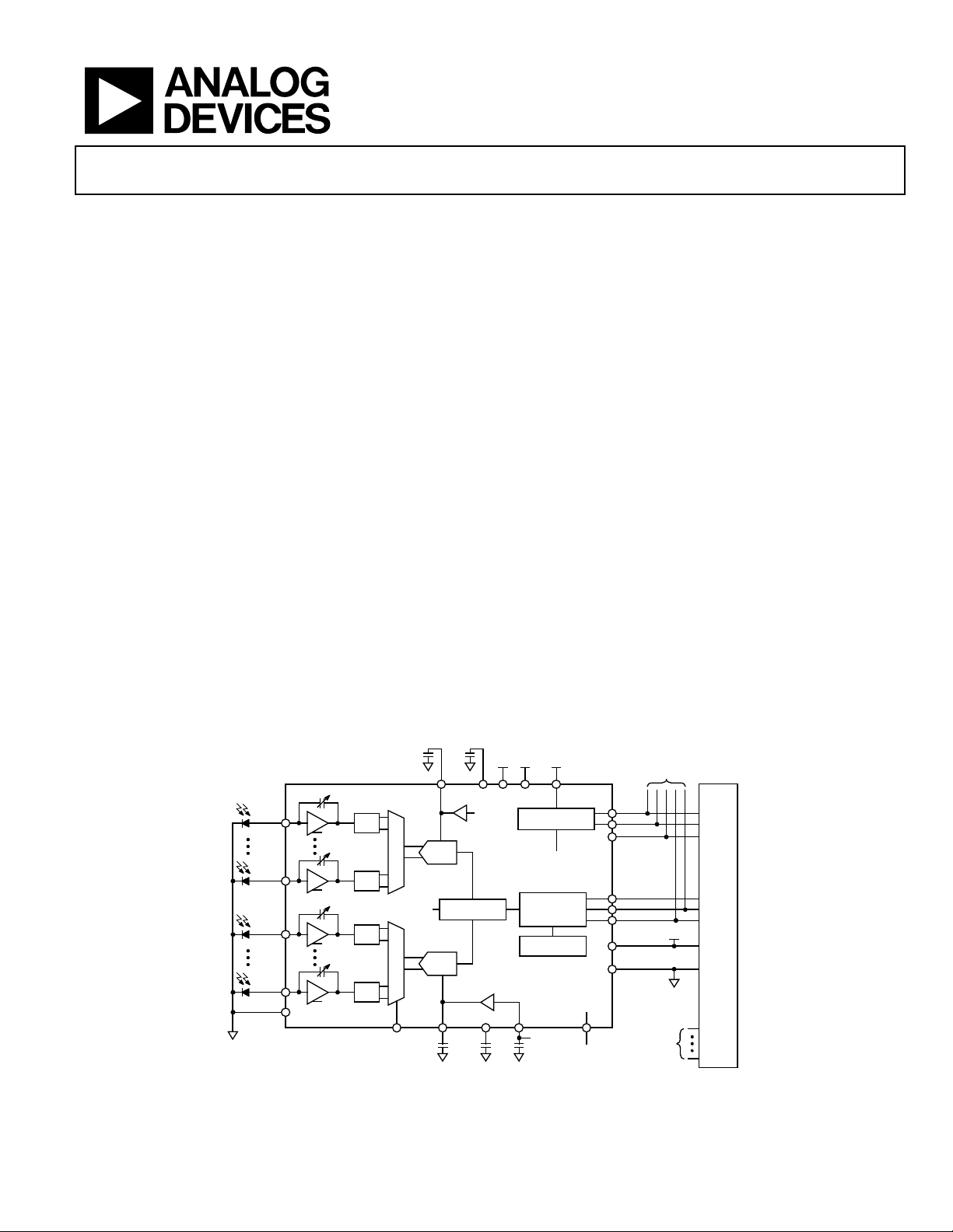
FUNCTIONAL BLOCK DIAGRAM
Rev. SpC
Information furnished by Analog Devices is believed to be accurate and reliable. However, no
responsibility is assumed by Analog Devices for its use, nor for any infringements of patents or other
rights of third parties that may result from its use. Specifications subject to change without notice. No
license is granted by implication or otherwise under any patent or patent rights of Analog Devices.
Trademarks and registered trademarks are the prop erty of their respective owner s.
Figure 1.
One Technology Way, P.O. Box 9106, Norwood, MA 02062-9106, U.S.A.
Tel: 781.329.4700 www.analog.com
Fax: 781.461.3113 ©2009–2010 Analog Devices, Inc. All rights reserved.
 Loading...