

Low Power, Selectable Gain
–
FEATURES
High performance at low power
High speed
−3 dB bandwidth of 750 MHz, G = 1
0.1 dB flatness to 210 MHz, V
Slew rate: 2900 V/μs, 25% to 75%
Fast 0.1% settling time of 9 ns
Low power: 9.5 mA per amplifier
Low harmonic distortion
108 dB SFDR @ 10 MHz
98 dB SFDR @ 20 MHz
Low output voltage noise: 9.2 nV/√Hz, G = 1, RTO
±0.2 mV typical input offset voltage
Selectable differential gains of 1, 2, and 3
Differential-to-differential or single-ended-to-differential
operation
Adjustable output common-mode voltage
Input common-mode range shifted down by 1 V
Wide supply range: +3 V to ±5 V
Available in 16-lead and 24-lead LFCSP packages
APPLICATIONS
ADC drivers
Single-ended-to-differential converters
IF and baseband gain blocks
Differential buffers
Line drivers
GENERAL DESCRIPTION
The ADA4950-1/ADA4950-2 are gain-selectable versions of the
ADA4932-1/ADA4932-2 with on-chip feedback and gain resistors.
They are ideal choices for driving high performance ADCs as singleended-to-differential or differential-to-differential amplifiers. The
output common-mode voltage is user adjustable by means of an
internal common-mode feedback loop, allowing the ADA4950-1/
ADA4950-2 output to match the input of the ADC. The internal
feedback loop also provides exceptional output balance as well
as suppression of even-order harmonic distortion products.
Differential gain configurations of 1, 2, and 3 are easily realized
with internal feedback networks that are connected externally
to set the closed-loop gain of the amplifier.
The ADA4950-1/ADA4950-2 are fabricated using the Analog
Devices, Inc., proprietary silicon-germanium (SiGe) complementary
bipolar process, enabling them to achieve low levels of distortion and
noise at low power consumption. The low offset and excellent
dynamic performance of the ADA4950-x make it well suited for
a wide variety of data acquisition and signal processing applications.
Rev. 0
Information furnished by Analog Devices is believed to be accurate and reliable. However, no
responsibility is assumed by Analog Devices for its use, nor for any infringements of patents or other
rights of third parties that may result from its use. Specifications subject to change without notice. No
license is granted by implication or otherwise under any patent or patent rights of Analog Devices.
Trademarks and registered trademarks are the property of their respective owners.
OUT, dm
= 2 V p-p, R
L, dm
BE
= 200 Ω
Differential ADC Driver, G = 1, 2, 3
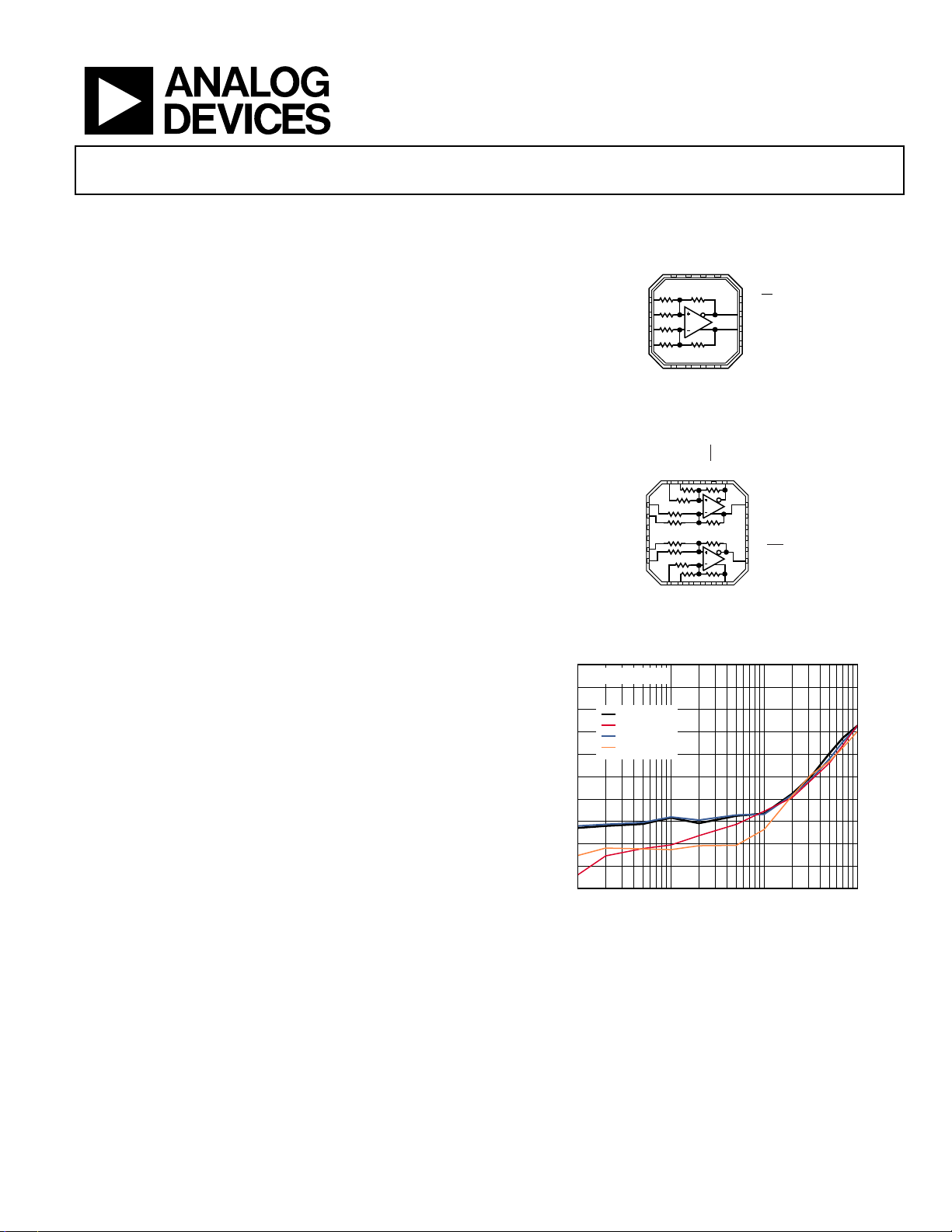
ADA4950-1/ADA4950-2
FUNCTIONAL BLOCK DIAGRAMS
1+INB
2+INA
3–INA
4+INB
1–INA1
2–INB1
3+V
S1
4+V
S1
5+INB2
6+INA2
40
V
=2V p-p
OUT, dm
–50
–60
–70
–80
–90
–100
–110
HARMONIC DISTORTION (dBc)
–120
–130
–140
0.1 1 10 100
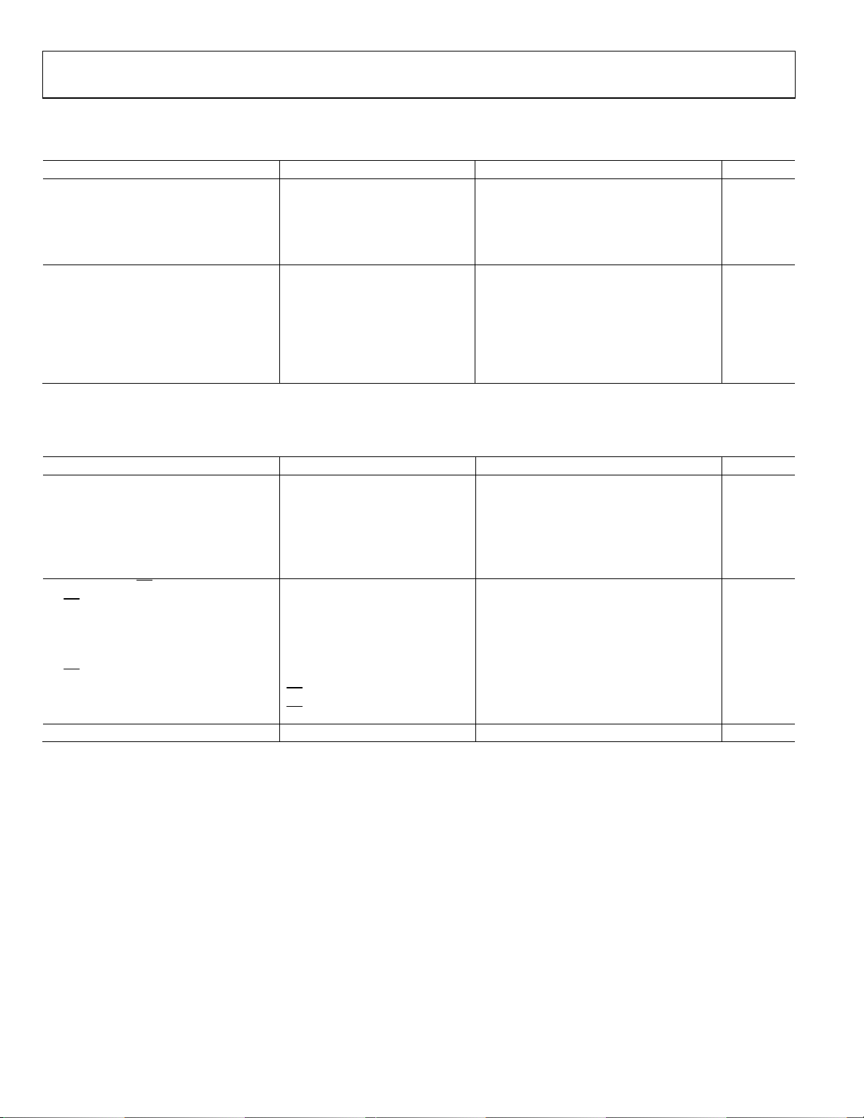
Figure 3. Harmonic Distortion vs. Frequency at Various Supplies
The ADA4950-x is available in a Pb-free, 3 mm × 3 mm, 16-lead
LFCSP (ADA4950-1, single) or a Pb-free, 4 mm × 4 mm, 24-lead
LFCSP (ADA4950-2, dual). The pinout has been optimized to
facilitate PCB layout and minimize distortion. The ADA4950-1/
ADA4950-2 are specified to operate over the −40°C to +105°C
temperature range; both operate on supplies from +3 V to ±5 V.
One Technology Way, P.O. Box 9106, Norwood, MA 02062-9106, U.S.A.
Tel: 781.329.4700 www.analog.com
Fax: 781.461.3113 ©2009 Analog Devices, Inc. All rights reserved.
HD2, ±5V
HD3, ±5V
HD2, ±2.5V
HD3, ±2.5V
S
S
S
S
–V
–V
–V
–V
14
13
15
16
ADA4950-1
5
6
S
S
+V
+V
12 PD
11 –OUT
10 +OUT
9V
8
7
S
S
+V
+V
Figure 1. ADA4950-1
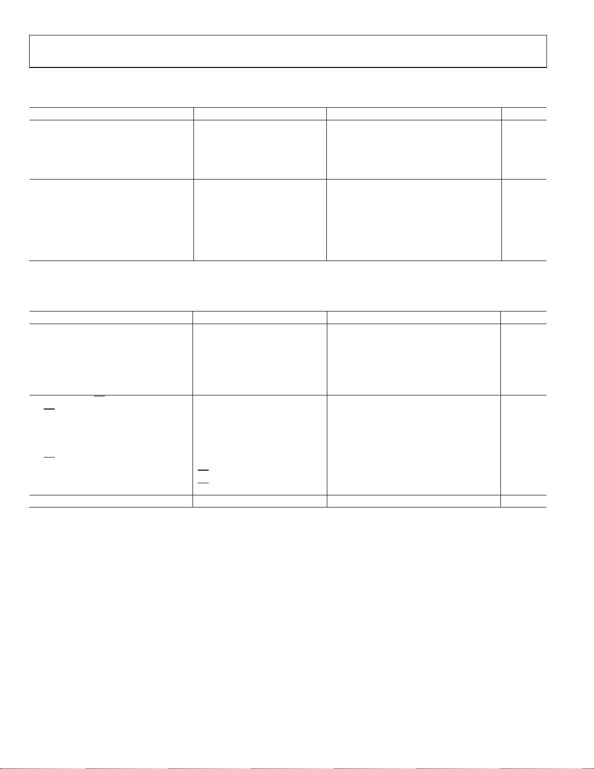
S1
S1
–V
–V
+INB1
+INA1
24
PD1
–OUT1
20
19
21
22
23
ADA4950-2
9
7
8
11
12
10
S2
S2
+V
+V
–INA2
OCM2
–INB2
V
+OUT2
Figure 2. ADA4950-2
FREQUENCY (MHz)
OCM
18 +OUT1
17 V
OCM1
16 –V
S2
–V
15
S2
14
PD2
13 –O UT2
07957-001
07957-002
07957-025

ADA4950-1/ADA4950-2
TABLE OF CONTENTS
Features .............................................................................................. 1
Applications ....................................................................................... 1
General Description ......................................................................... 1
Functional Block Diagrams ............................................................. 1
Revision History ............................................................................... 2
Specifications ..................................................................................... 3
±5 V Operation ............................................................................. 3
5 V Operation ............................................................................... 5
Absolute Maximum Ratings ............................................................ 7
Thermal Resistance ...................................................................... 7
Maximum Power Dissipation ..................................................... 7
ESD Caution .................................................................................. 7
Pin Configurations and Function Descriptions ........................... 8
Typical Performance Characteristics ............................................. 9
Test Circuits ..................................................................................... 16
Ter minology .................................................................................... 17
Theory of Operation ...................................................................... 18
Applications Information .............................................................. 19
Analyzing an Application Circuit ............................................ 19
Selecting the Closed-Loop Gain ............................................... 19
Estimating the Output Noise Voltage ...................................... 19
Calculating the Input Impedance for an Application Circuit
....................................................................................................... 20
Input Common-Mode Voltage Range ..................................... 22
Input and Output Capacitive AC Coupling ............................ 22
Input Signal Swing Considerations .......................................... 22
Setting the Output Common-Mode Voltage .......................... 22
Layout, Grounding, and Bypassing .............................................. 23
High Performance ADC Driving ................................................. 24
Outline Dimensions ....................................................................... 25
Ordering Guide .......................................................................... 25
REVISION HISTORY
5/09—Revision 0: Initial Version
Rev. 0 | Page 2 of 28

ADA4950-1/ADA4950-2
SPECIFICATIONS
±5 V OPERATION
TA = 25°C, +VS = 5 V, −VS = −5 V, V
refer to single-ended input and differential outputs, unless otherwise noted. Refer to Figure 52 for signal definitions.
Differential Inputs to V
OUT, dm
Table 1.
Parameter Test Conditions/Comments Min Typ Max Unit
DYNAMIC PERFORMANCE
−3 dB Small-Signal Bandwidth V
−3 dB Large-Signal Bandwidth V
Bandwidth for 0.1 dB Flatness V
ADA4950-1 210 MHz
ADA4950-2 230 MHz
Slew Rate V
Settling Time to 0.1% V
Overdrive Recovery Time VIN = 0 V to 5 V ramp, G = 2 20 ns
NOISE/HARMONIC PERFORMANCE See Figure 51 for distortion test circuit
Second Harmonic V
1 MHz −108 dBc
10 MHz −107 dBc
20 MHz −98 dBc
50 MHz −80 dBc
Third Harmonic V
1 MHz −126 dBc
10 MHz −105 dBc
20 MHz −99 dBc
50 MHz −84 dBc
IMD3 f1 = 30 MHz, f2 = 30.1 MHz, V
Voltage Noise (Referred to Output) f = 1 MHz
Gain = 1 9.2 nV/√Hz
Gain = 2 12.5 nV/√Hz
Gain = 3 16.6 nV/√Hz
Crosstalk (ADA4950-2)
INPUT CHARACTERISTICS
Offset Voltage (Referred to Input) V
T
Input Capacitance Single-ended at package pin 0.5 pF
Input Common-Mode Voltage Range
CMRR DC, ∆V
Open-Loop Gain 64 66 dB
OUTPUT CHARACTERISTICS
Output Voltage Swing
Linear Output Current 200 kHz, R
Output Balance Error
Gain Error Gain = 1 0.5 1.2 %
Gain = 2 1.0 1.9 %
Gain = 3 0.8 1.7 %
= 0 V, G = 1, RT = 53.6 (when used), R
OCM
Performance
= 0.1 V p-p 750 MHz
OUT, dm
= 2.0 V p-p 350 MHz
OUT, dm
= 2.0 V p-p, RL = 200 Ω
OUT, dm
= 2 V p-p, 25% to 75% 2900 V/μs
OUT, dm
= 2 V step 9 ns
OUT, dm
= 2 V p-p
OUT, dm
= 2 V p-p
OUT, dm
f = 10 MHz; Channel 2 active, Channel 1
output
= V
= V
+DIN
−DIN
to T
MIN
MAX
Directly at internal amplifier inputs, not
external input terminals
OUT, dm
Maximum ∆V
= 1 kΩ
R
L
/∆V
∆V
OUT, cm
see Figure 50 for output balance test circuit
= 0 V −2.5 ±0.2 +2.5 mV
OCM
variation –3.7 μV/°C
/∆V
, ∆V
IN, cm
, single-ended output,
OUT
= 10 Ω, SFDR = 69 dB 114 mA peak
L, dm
, ∆V
OUT, dm
OUT, dm
= 1 kΩ, unless otherwise noted. All specifications
L, dm
= 2 V p-p −94 dBc
OUT, dm
−87 dB
= ±1 V −64 −49 dB
IN, cm
–V
+ 1.4 to
S
– 1.4
+V
S
= 2 V p-p, 1 MHz;
−62 dB
−V
+V
−V
+V
+ 0.2 to
S
− 1.8
S
+ 1.2 to
S
− 1.2
S
V
V
Rev. 0 | Page 3 of 28
ADA4950-1/ADA4950-2
V
to V
OCM
Table 2.
Parameter Test Conditions/Comments Min Typ Max Unit
V
DYNAMIC PERFORMANCE
OCM
−3 dB Small-Signal Bandwidth V
−3 dB Large-Signal Bandwidth V
Slew Rate VIN = 1.5 V to 3.5 V, 25% to 75% 430 V/μs
Input Voltage Noise (Referred to Input) f = 1 MHz 9.8 nV/√Hz
V
INPUT CHARACTERISTICS
OCM
Input Voltage Range
Input Resistance 22 26 32 kΩ
Input Offset Voltage V
V
CMRR ΔV
OCM
Gain ΔV
General Performance
Table 3.
Parameter Test Conditions/Comments Min Typ Max Unit
POWER SUPPLY
Operating Range 3.0 11 V
Quiescent Current per Amplifier 8.8 9.5 10.1 mA
T
Powered down 0.7 1.0 mA
Power Supply Rejection Ratio ΔV
POWER-DOWN (PD)
PD Input Voltage
Enabled ≥(+VS – 1.8) V
Turn-Off Time 600 ns
Turn-On Time 28 ns
PD Pin Bias Current per Amplifier
Enabled
Disabled
OPERATING TEMPERATURE RANGE −40 +105 °C
Performance
OUT, cm
= 100 mV p-p 250 MHz
OUT, cm
= 2 V p-p 105 MHz
OUT, cm
+ 1.2 to
–V
S
+V
– 1.2
S
= V
+DIN
OUT, dm
OUT, cm
MIN
OUT, dm
= 0 V −6 +0.8 +6 mV
−DIN
/ΔV
, ΔV
OCM
/ΔV
OCM
to T
variation 31 μA/°C
MAX
= ±1 V −60 −49 dB
OCM
, ΔV
= ±1 V 0.98 1.0 1.01 V/V
OCM
/ΔVS, ΔVS = 1 V p-p −96 −84 dB
V
Powered down ≤(+V
– 2.5) V
S
PD
PD
= 5 V
= 0 V
−1.0 +0.2 +1.0 μA
−250 −180 −140 μA
Rev. 0 | Page 4 of 28

ADA4950-1/ADA4950-2
5 V OPERATION
TA = 25°C, +VS = 5 V, −VS = 0 V, V
refer to single-ended input and differential outputs, unless otherwise noted. Refer to Figure 52 for signal definitions.
Differential Inputs to V
OUT, dm
Table 4.
Parameter Test Conditions/Comments Min Typ Max Unit
DYNAMIC PERFORMANCE
−3 dB Small-Signal Bandwidth V
−3 dB Large-Signal Bandwidth V
Bandwidth for 0.1 dB Flatness V
ADA4950-1 220 MHz
ADA4950-2 160 MHz
Slew Rate V
Settling Time to 0.1% V
Overdrive Recovery Time VIN = 0 V to 2.5 V ramp, G = 2 19 ns
NOISE/HARMONIC PERFORMANCE See Figure 51 for distortion test circuit
Second Harmonic V
1 MHz −108 dBc
10 MHz −107 dBc
20 MHz −98 dBc
50 MHz −82 dBc
Third Harmonic V
1 MHz −124 dBc
10 MHz −114 dBc
20 MHz −99 dBc
50 MHz −83 dBc
IMD3 f1 = 30 MHz, f2 = 30.1 MHz, V
Voltage Noise (Referred to Input) f = 1 MHz
Gain = 1 9.2 nV/√Hz
Gain = 2 12.5 nV/√Hz
Gain = 3 16.6 nV/√Hz
Crosstalk (ADA4950-2)
INPUT CHARACTERISTICS
Offset Voltage (Referred to Input) V
T
Input Capacitance Single-ended at package pin 0.5 pF
Input Common-Mode Voltage Range
CMRR DC, ∆V
Open-Loop Gain 64 66 dB
OUTPUT CHARACTERISTICS
Output Voltage Swing
Linear Output Current 200 kHz, R
Output Balance Error
Gain Error Gain = 1 0.5 1.2 %
Gain = 2 1.0 1.9 %
Gain = 3 0.8 1.7 %
= 2.5 V, G = 1, RT = 53.6 (when used), R
OCM
Performance
= 0.1 V p-p 770 MHz
OUT, dm
= 2.0 V p-p 320 MHz
OUT, dm
= 2.0 V p-p, RL = 200 Ω
OUT, dm
= 2 V p-p, 25% to 75% 2200 V/μs
OUT, dm
= 2 V step 10 ns
OUT, dm
= 2 V p-p
OUT, dm
= 2 V p-p
OUT, dm
f = 10 MHz; Channel 2 active, Channel 1
output
= V
= V
+DIN
−DIN
to T
MIN
MAX
Directly at internal amplifier inputs, not
external input terminals
OUT, dm
Maximum ∆V
= 1 kΩ
R
L
/∆V
∆V
OUT, cm
see Figure 50 for output balance test circuit
= 2.5 V −4 ±0.4 +4 mV
OCM
variation −3.7 μV/°C
/∆V
, ∆V
IN, cm
IN, cm
, single-ended output,
OUT
= 10 Ω, SFDR = 67 dB 70 mA peak
L, dm
, ∆V
OUT, dm
OUT, dm
= 1 kΩ, unless otherwise noted. All specifications
L, dm
= 2 V p-p −94 dBc
OUT, dm
−87 dB
–V
+V
S
S
+ 0.2 to
– 1.8
V
= ±1 V −64 −49 dB
V
= 1 V p-p, 1 MHz;
–V
+V
S
+ 1.2 to
– 1.2
S
–V
+V
S
S
+ 1.1 to
– 1.1
−62 dB
Rev. 0 | Page 5 of 28
ADA4950-1/ADA4950-2
V
to V
OCM
Table 5.
Parameter Test Conditions/Comments Min Typ Max Unit
V
DYNAMIC PERFORMANCE
OCM
−3 dB Small-Signal Bandwidth V
−3 dB Large-Signal Bandwidth V
Slew Rate VIN = 1.5 V to 3.5 V, 25% to 75% 380 V/μs
Input Voltage Noise (Referred to Input) f = 1 MHz 9.8 nV/√Hz
V
INPUT CHARACTERISTICS
OCM
Input Voltage Range
Input Resistance 22 26 32 kΩ
Input Offset Voltage V
V
CMRR ΔV
OCM
Gain ΔV
General Performance
Table 6.
Parameter Test Conditions/Comments Min Typ Max Unit
POWER SUPPLY
Operating Range 3.0 11 V
Quiescent Current per Amplifier 8.4 8.9 9.6 mA
T
Powered down 0.6 0.9 mA
Power Supply Rejection Ratio ΔV
POWER-DOWN (PD)
PD Input Voltage
Enabled ≥(+VS – 1.8) V
Turn-Off Time 600 ns
Turn-On Time 29 ns
PD Pin Bias Current per Amplifier
Enabled
Disabled
OPERATING TEMPERATURE RANGE −40 +105 °C
Performance
OUT, cm
= 100 mV p-p 240 MHz
OUT, cm
= 2 V p-p 90 MHz
OUT, cm
+ 1.2 to
–V
S
+V
– 1.2
S
= V
+DIN
OUT, dm
OUT, cm
MIN
OUT, dm
= 2.5 V −6.5 +1.0 +6.5 mV
−DIN
/ΔV
, ΔV
OCM
/ΔV
OCM
to T
variation 31 μA/°C
MAX
= ±1 V −60 −49 dB
OCM
, ΔV
= ±1 V 0.98 1.0 1.01 V/V
OCM
/ΔVS, ΔVS = 1 V p-p −96 −84 dB
V
Powered down ≤(+V
– 2.5) V
S
PD
PD
= 5 V
= 0 V
−1.0 +0.2 +1.0 μA
−100 −65 −40 μA
Rev. 0 | Page 6 of 28
ADA4950-1/ADA4950-2
ABSOLUTE MAXIMUM RATINGS
Table 7.
Parameter Rating
Supply Voltage 11 V
Power Dissipation See Figure 4
Input Current, +INx, −INx, PD
±5 mA
Storage Temperature Range −65°C to +125°C
Operating Temperature Range
ADA4950-1 −40°C to +105°C
ADA4950-2 −40°C to +105°C
Lead Temperature (Soldering, 10 sec) 300°C
Junction Temperature 150°C
The power dissipated in the package (P
cent power dissipation and the power dissipated in the package
due to the load drive. The quiescent power is the voltage between
the supply pins (V
dissipated due to the load drive depends upon the particular
application. The power dissipated due to the load drive is calculated by multiplying the load current by the associated voltage
drop across the device. RMS voltages and currents must be used
in these calculations.
Airflow increases heat dissipation, effectively reducing θ
addition, more metal directly in contact with the package leads/
exposed pad from metal traces, through holes, ground, and
Stresses above those listed under Absolute Maximum Ratings
may cause permanent damage to the device. This is a stress
rating only; functional operation of the device at these or any
other conditions above those indicated in the operational
section of this specification is not implied. Exposure to absolute
maximum rating conditions for extended periods may affect
device reliability.
THERMAL RESISTANCE
θJA is specified for the device (including exposed pad) soldered
to a high thermal conductivity 2s2p printed circuit board, as
power planes reduces θ
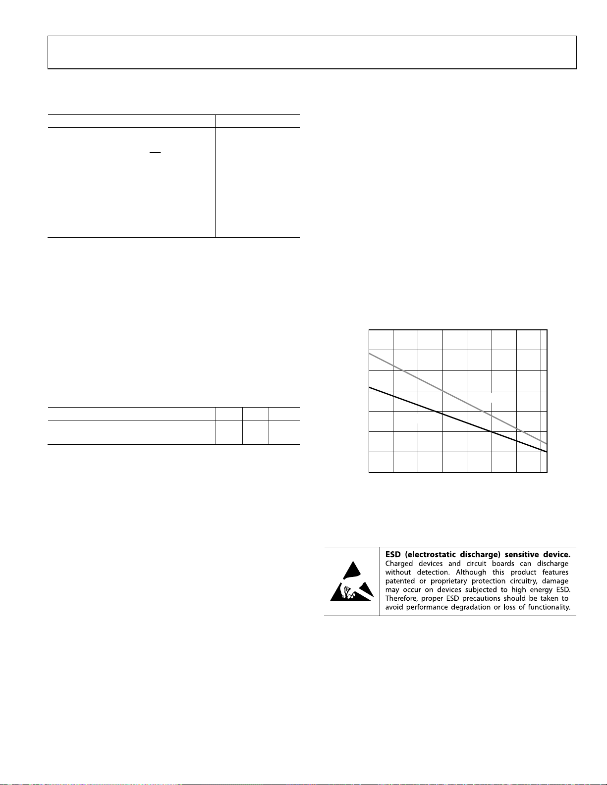
Figure 4 shows the maximum safe power dissipation in the
package vs. the ambient temperature for the single 16-lead
LFCSP (91°C/W) and the dual 24-lead LFCSP (65°C/W) on
a JEDEC standard 4-layer board with the exposed pad soldered
to a PCB pad that is connected to a solid plane.
3.5
3.0
2.5
described in EIA/JESD51-7.
2.0
Table 8. Thermal Resistance
Package Type θJA θJC Unit
ADA4950-1, 16-Lead LFCSP (Exposed Pad) 91 28 °C/W
ADA4950-2, 24-Lead LFCSP (Exposed Pad) 65 16 °C/W
MAXIMUM POWER DISSIPATION
The maximum safe power dissipation in the ADA4950-x package
is limited by the associated rise in junction temperature (T
the die. At approximately 150°C, which is the glass transition
) on
J
1.5
1.0
MAXIMUM POWER DISSIPATI ON (W)
0.5
0
–40 –20 0 20 40
Figure 4. Maximum Power Dissipation vs. Ambient Temperature
temperature, the plastic changes its properties. Even temporarily
exceeding this temperature limit can change the stresses that the
package exerts on the die, permanently shifting the parametric
ESD CAUTION
performance of the ADA4950-x. Exceeding a junction temperature of 150°C for an extended period can result in changes in
the silicon devices, potentially causing failure.
) times the quiescent current (IS). The power
S
.
JA
ADA4950-1
AMBIENT TEM PE RATURE (°C)
for a 4-Layer Board
) is the sum of the quies-
D
JA
ADA4950-2
60 80 100
. In
07957-004
Rev. 0 | Page 7 of 28
ADA4950-1/ADA4950-2
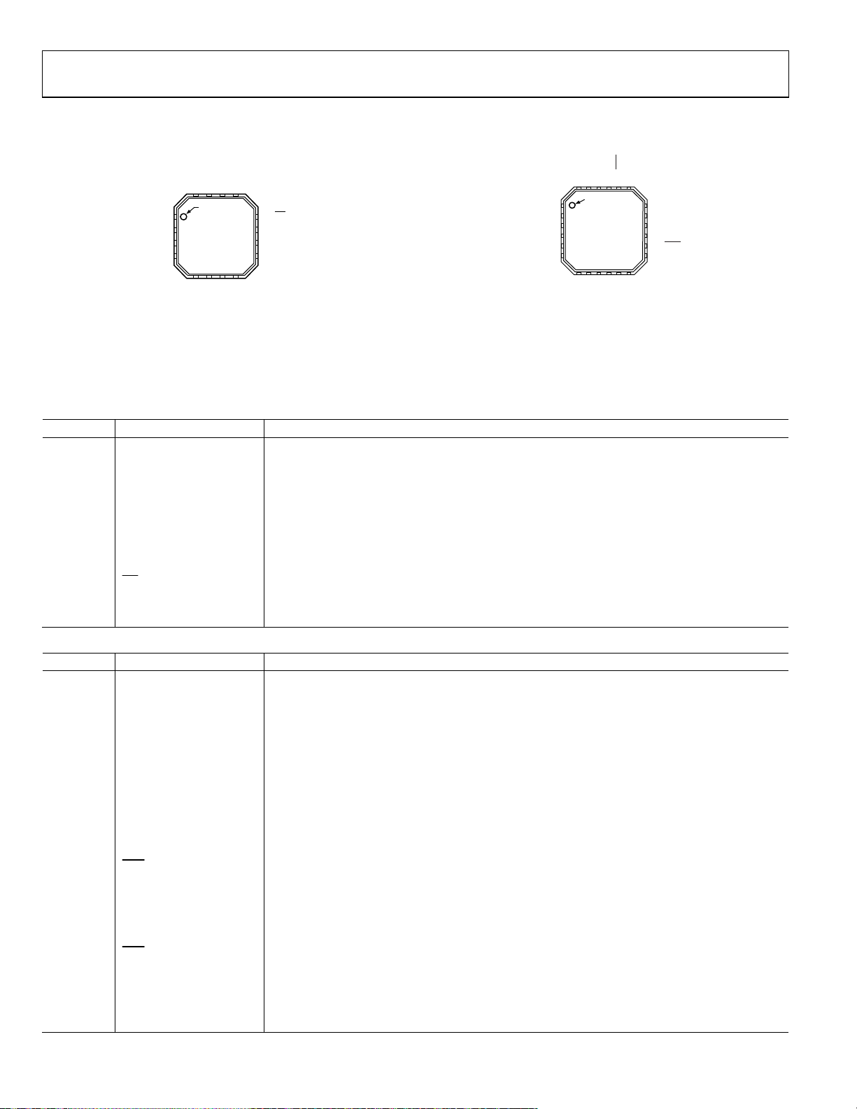
PIN CONFIGURATIONS AND FUNCTION DESCRIPTIONS
1
2
3
ADA4950-2
4
5
6
1
–VS1–VS1+INB1
+INA
21
22
23
24
PIN 1
INDICATOR
TOP VIEW
(Not to Scale)
9
7
8
10
S2
S2
+V
+V
–INA2
–INB2
PD1
–OUT1
20
19
18
+OUT1
17
V
OCM1
16
–V
S2
–V
15
S2
14
PD2
13
–OUT2
11
12
OCM2
V
+OUT2
07957-006
S
S
S
S
–V
–V
–V
–V
14
13
15
16
PIN 1
INDICAT OR
1+INB
2+INA
ADA4950-1
TOP VIEW
3–INA
(Not to Scale)
4–INB
5
6
S
S
+V
+V
NOTES
1. SOLDER THE EXPOSED PADDLE ON THE BACK OF
THE PACKAGE TO A GROUND PLANE O R TO A
POWER PLANE.
12 PD
11 –OUT
10 +OUT
9V
OCM
8
7
S
S
+V
+V
Figure 5. ADA4950-1 Pin Configuration
07957-005
–INA1
–INB1
+V
S1
+V
S1
+INB2
+INA2
NOTES
1. SOLDER THE E XPOSED PADDLE ON THE BACK OF
THE PACKAGE TO A GROUND PLANE O R TO A
POWE R PLANE.
Figure 6. ADA4950-2 Pin Configuration
Table 9. ADA4950-1 Pin Function Descriptions
Pin No. Mnemonic Description
1 +INB Positive Input B, 250 Ω Input. Use alone for G = 2 or tie to +INA for G = 3.
2 +INA Positive Input A, 500 Ω Input. Use alone for G = 1 or tie to +INB for G = 3.
3 −INA Negative Input A, 500 Ω Input. Use alone for G = 1 or tie to −INB for G = 3.
4 −INB Negative Input B, 250 Ω Input. Use alone for G = 2 or tie to −INA for G = 3.
5 to 8 +VS Positive Supply Voltage.
9 V
Output Common-Mode Voltage.
OCM
10 +OUT Positive Output.
11 −OUT Negative Output.
12
PD
Power-Down Pin.
13 to 16 −VS Negative Supply Voltage.
17 (EPAD) Exposed Paddle (EPAD) Solder the exposed paddle on the back of the package to a ground plane or to a power plane.
Table 10. ADA4950-2 Pin Function Descriptions
Pin No. Mnemonic Description
1 −INA1 Negative Input A, Amplifier 1, 500 Ω Input. Use alone for G = 1 or tie to –INB1 for G = 3.
2 −INB1 Negative Input B, Amplifier 1, 250 Ω Input. Use alone for G = 2 or tie to –INA1 for G = 3.
3, 4 +VS1 Positive Supply Voltage, Amplifier 1.
5 +INB2 Positive Input B, Amplifier 2, 250 Ω Input. Use alone for G = 2 or tie to +INA2 for G = 3.
6 +INA2 Positive Input A, Amplifier 2, 500 Ω Input. Use alone for G = 1 or tie to +INB2 for G = 3.
7 −INA2 Negative Input A, Amplifier 2, 500 Ω Input. Use alone for G = 1 or tie to –INB2 for G = 3.
8 −INB2 Negative Input B, Amplifier 2, 250 Ω Input. Use alone for G = 2 or tie to –INA2 for G = 3.
9, 10 +VS2 Positive Supply Voltage, Amplifier 2.
11 V
Output Common-Mode Voltage, Amplifier 2.
OCM2
12 +OUT2 Positive Output, Amplifier 2.
13 −OUT2 Negative Output, Amplifier 2.
14
PD2
Power-Down Pin, Amplifier 2.
15, 16 −VS2 Negative Supply Voltage, Amplifier 2.
17 V
Output Common-Mode Voltage, Amplifier 1.
OCM1
18 +OUT1 Positive Output, Amplifier 1.
19 −OUT1 Negative Output, Amplifier 1.
20
PD1
Power-Down Pin, Amplifier 1.
21, 22 −VS1 Negative Supply Voltage, Amplifier 1.
23 +INB1 Positive Input B, Amplifier 1, 250 Ω Input. Use alone for G = 2 or tie to +INA1 for G = 3.
24 +INA1 Positive Input A, Amplifier 1, 500 Ω Input. Use alone for G = 1 or tie to +INB1 for G = 3.
25 (EPAD) Exposed Paddle (EPAD) Solder the exposed paddle on the back of the package to a ground plane or to a power plane.
Rev. 0 | Page 8 of 28
ADA4950-1/ADA4950-2
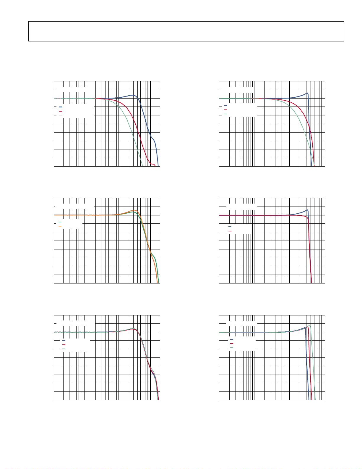
TYPICAL PERFORMANCE CHARACTERISTICS
TA = 25°C, +VS = 5 V, −VS = −5 V, V
for test setup. Refer to Figure 52 for signal definitions.
2
V
OUT, dm
G = 1, R
G = 2, R
G = 3, R
= 100mV p-p
= 53.6Ω
T
= 57.6Ω
T
= 61.9Ω
T
10 100
FREQUENCY ( MHz)
1
0
–1
–2
–3
–4
–5
–6
NORMALIZED CLOSED-L OOP GAIN (dB)
–7
–8
1
Figure 7. Small-Signal Frequency Response for Various Gains
= 0 V, G = 1, RT = 53.6 Ω (when used), R
OCM
1000
07957-007
= 1 kΩ, unless otherwise noted. Refer to Figure 49
L, dm
2
V
OUT, dm
G = 1, R
G = 2, R
G = 3, R
= 2V p-p
= 53.6Ω
T
= 57.6Ω
T
= 61.9Ω
T
10 100 1000
FREQUENCY ( MHz)
1
0
–1
–2
–3
–4
–5
–6
NORMALIZED CLOSED-L OOP GAIN (dB)
–7
–8
1
Figure 10. Large-Signal Frequency Response for Various Gains
07957-010
2
V
OUT, dm
VS= ±5V
V
S
= 100mV p-p
= ±2.5V
10 100
FREQUENCY ( MHz)
1000
1
0
–1
–2
–3
–4
–5
CLOSED-LOOP GAIN (dB)
–6
–7
–8
1
Figure 8. Small-Signal Frequency Response for Various Supplies
2
V
OUT, dm
TA = –40°C
T
T
= 100mV p-p
= +25°C
A
= +105°C
A
10 100
FREQUENCY ( MHz)
1000
1
0
–1
–2
–3
–4
–5
CLOSED-LOOP GAIN (dB)
–6
–7
–8
1
Figure 9. Small-Signal Frequency Response for Various Temperatures
2
V
OUT, dm
V
S
V
S
= 2V p-p
= ±5V
= ±2.5V
10 100 1000
FREQUENCY ( MHz)
07957-011
1
0
–1
–2
–3
–4
–5
CLOSED-LOOP GAIN (dB)
–6
–7
07957-008
–8
1
Figure 11. Large-Signal Frequency Response for Various Supplies
2
V
OUT, dm
T
A
T
A
T
A
= 2V p-p
= –40°C
= +25°C
= +105°C
10 100 1000
FREQUENCY ( MHz)
07957-012
1
0
–1
–2
–3
–4
–5
CLOSED-LOOP GAIN (dB)
–6
–7
07957-009
–8
1
Figure 12. Large-Signal Frequency Response for Various Temperatures
Rev. 0 | Page 9 of 28

ADA4950-1/ADA4950-2
2
V
OUT, dm
= 100mV p-p
1
0
–1
–2
R
L
R
L
= 1kΩ
= 200Ω
–3
–4
–5
CLOSED-LOOP GAIN (dB)
–6
–7
–8
1
10 100 1000
FREQUENCY ( MHz)
Figure 13. Small-Signal Frequency Response at Various Loads
07957-013
2
V
OUT, dm
= 2V p-p
1
0
–1
–2
R
R
= 1kΩ
L
= 200Ω
L
–3
–4
–5
CLOSED-LOOP GAIN (dB)
–6
–7
–8
1
10 100 1000
FREQUENCY ( MHz)
Figure 16. Large-Signal Frequency Response at Various Loads
07957-016
2
V
OUT, dm
= 100mV p-p
1
0
–1
–2
–3
V
OCM
V
OCM
V
OCM
= –2.5VDC
= 0V
= +2.5VDC
–4
–5
CLOSED-LOOP GAIN (dB)
–6
–7
–8
1
10 100
FREQUENCY ( MHz)
Figure 14. Small-Signal Frequency Response for Various V
4
V
= 100mV p-p
OUT, dm
2
0
CL= 0pF
C
–2
–4
CLOSED-LOOP GAIN (dB)
–6
L
C
L
C
L
= 0.9pF
= 1.8pF
= 2.7pF
1000
OCM
Levels
2
V
OUT, dm
= 2V p-p
1
0
–1
–2
V
V
V
OCM
OCM
OCM
= –2.5VDC
= 0V
= +2.5VDC
–3
–4
–5
CLOSED-LOOP GAIN (dB)
–6
–7
07957-014
–8
1
10 100
07957-017
1000
FREQUENCY ( MHz)
Figure 17. Large-Signal Frequency Response for Various V
OCM
Levels
4
V
= 2V p-p
OUT, dm
2
0
C
= 0pF
L
C
= 0.9pF
–2
L
C
L
C
L
= 1.8pF
= 2.7pF
–4
CLOSED-LOOP GAIN (dB)
–6
–8
1
10 100
07957-015
1000
FREQUENCY ( MHz)
Figure 15. Small-Signal Frequency Response at Various Capacitive Loads
Rev. 0 | Page 10 of 28
–8
1
10 100 1000
07957-018
FREQUENCY ( MHz)
Figure 18. Large-Signal Frequency Response at Various Capacitive Loads

ADA4950-1/ADA4950-2
0.5
V
= 100mV p-p
OUT, dm
0.4
0.3
0.2
0.1
0
–0.1
–0.2
CLOSED-LOOP GAIN (dB)
–0.3
–0.4
–0.5
ADA4950-1, RL=1kΩ
ADA4950-1, RL= 200Ω
ADA4950-2, AMP 1, RL=1kΩ
ADA4950-2, AMP 1, RL=200Ω
ADA4950-2, AMP 2, RL=1kΩ
ADA4950-2, AMP 2, RL=200Ω
1 10 100 1000
FREQUENCY ( MHz)
Figure 19. 0.1 dB Flatness, Small-Signal Frequency Response for Various
Loads
2
1
V
(AC) = 100mV p-p
OCM
0
–1
–2
–3
GAIN (dB)
–4
OCM
V
–5
–6
–7
–8
1
Figu re 20. V
= –2.5VDC
V
OCM
V
= 0V
OCM
V
= +2.5VDC
OCM
10 100
FREQUENCY ( MHz)
Small-Signal Frequency Response at Various DC Levels
OCM
1000
0.5
V
= 2V p-p
OUT, dm
0.4
0.3
0.2
0.1
0
–0.1
–0.2
CLOSED-LOOP GAIN (dB)
–0.3
–0.4
07957-019
–0.5
ADA4950-1, RL=1kΩ
ADA4950-1, RL= 200Ω
ADA4950-2, AMP 1, RL=1kΩ
ADA4950-2, AMP 1, RL= 200Ω
ADA4950-2, AMP 2, RL=1kΩ
ADA4950-2, AMP 2, RL= 200Ω
1 10 100 1000
FREQUENCY (MHz)
07957-022
Figure 22. 0.1 dB Flatness, Large-Signal Frequency Response for Various Loads
2
V
(AC) = 2V p-p
OCM
1
0
–1
V
= –2.5VDC
OCM
–2
V
= 0V
OCM
V
= +2.5VDC
OCM
–3
GAIN (dB)
–4
OCM
V
–5
–6
–7
07957-020
–8
1
Figu re 23. V
10 100 1000
FREQUE NCY (MHz)
Large-Signal Frequency Response at Various DC Levels
OCM
07957-023
–40
V
=2V p-p
OUT, dm
–50
HARMONIC DISTORTION (dBc)
–60
–70
–80
–90
–100
–110
–120
–130
–140
HD2, R
HD3, R
HD2, R
HD3, R
0.1 1 10 100
=1kΩ
L, dm
=1kΩ
L, dm
=200Ω
L, dm
=200Ω
L, dm
FREQUENCY (MHz)
Figure 21. Harmonic Distortion vs. Frequency at Various Loads
07957-021
Rev. 0 | Page 11 of 28
–40
V
=2V p-p
OUT, dm
–50
–60
–70
–80
–90
–100
–110
HARMONIC DISTORTION (dBc)
–120
–130
–140
0.1 1 10 100
HD2, G = 1
HD3, G = 1
HD2, G = 2
HD3, G = 2
HD2, G = 3
HD3, G = 3
FREQUENCY (MHz)
Figure 24. Harmonic Distortion vs. Frequency at Various Gains
07957-024

ADA4950-1/ADA4950-2
–40
V
=2V p-p
OUT, dm
–50
–60
–70
–80
–90
–100
–110
HARMONIC DISTORTION (dBc)
–120
–130
–140
0.1 1 10 100
HD2, ±5V
HD3, ±5V
HD2, ±2.5V
HD3, ±2.5V
FREQUENCY (MHz)
Figure 25. Harmonic Distortion vs. Frequency at Various Supplies
07957-025
–40
–50
V
= 0V
OCM
–60
HD2, ±5V
HD3, ±5V
–70
HD2, ±2.5V
–80
HD3, ±2.5V
–90
–100
–110
HARMONIC DISTORTION (dBc)
–120
–130
–140
01234567
Figure 28. Harmonic Distortion vs. V
V
OUT, dm
891011121314
(V p-p)
, f = 10 MHz
OUT, dm
07957-028
–30
V
=2V p-p
OUT, dm
–40
–50
HD2, V
HD3, V
HD2, V
HD3, V
HD2 AT 10MHz
HD3 AT 10MHz
HD2 AT 30MHz
HD3 AT 30MHz
–1 0 1 2 3 4
V
(V)
OCM
at Various Frequencies, ±5 V Supplies
OCM
=2V p-p
OUT, dm
=2V p-p
OUT, dm
=4V p-p
OUT, dm
=4V p-p
OUT, dm
FREQUENCY (MHz)
–60
–70
–80
–90
–100
HARMONIC DISTORTION (dBc)
–110
–120
–130
–4 –3 –2
Figure 26. Harmonic Distortion vs. V
–40
–50
–60
–70
–80
–90
–100
–110
HARMONIC DISTORTION (dBc)
–120
–130
–140
0.1 1 10 100
Figure 27. Harmonic Distortion vs. Frequency at Various V
OUT, dm
–40
V
= 2V p-p
OUT, dm
–50
–60
–70
–80
–90
–100
HARMONIC DIST ORTION (dBc)
–110
–120
07957-026
1.6 1.8 2.0 2.2 2.4 2.6 2.8 3.0 3.2 3.4 3.6 3.8
1.2 1.4
Figure 29. Harmonic Distortion vs. V
–50
V
=2V p-p
OUT, dm
–60
–70
–80
–90
–100
–110
–120
–130
SPURIOUS-F REE DYNAMIC RANGE ( dBc)
–140
0.1 1 10 100
07957-027
Figure 30. Spurious-Free Dynamic Range vs. Frequency at Various Loads
R
HD2 AT 10MHz
HD3 AT 10MHz
HD2 AT 30MHz
HD3 AT 30MHz
V
=200Ω
L, dm
FREQUENCY (MHz)
(V)
OCM
at Various Frequencies, 5 V Supply
OCM
=1kΩ
R
L, dm
07957-029
07957-030
Rev. 0 | Page 12 of 28

ADA4950-1/ADA4950-2
10
V
= 2V p-p
OUT, dm
0
–10
–20
–30
–40
–50
–60
–70
–80
–90
NORMALIZE D SPECTRUM (dB)
–100
–110
–120
29.6 29.7 29.8 29. 9 30. 0 30.1 30.2 30.3 30.4 30.5
FREQUENCY (MHz)
Figure 31. 30 MHz Intermodulation Distortion
07957-031
80
60
40
20
0
GAIN (dB)
–20
–40
–60
–80
1k 10k 100k 1M 10M 100M 1G 10G
FREQUENCY (Hz)
GAIN
PHASE
Figure 34. Open-Loop Gain and Phase vs. Frequency
90
45
0
–45
–90
–135
–180
–225
–270
PHASE (Degrees)
07957-240
–45
R
= 200Ω
–47
–49
–51
–53
–55
CMRR (dB)
–57
–59
–61
–63
–65
L, dm
V
= 2V p-p
IN
1 10 100 1000
FREQUENCY (MHz)
Figure 32. CMRR vs. Frequency
0
V
=2Vp-p
OUT, dm
–10
–20
–30
–40
–50
OUTPUT BALANCE (dB)
0
R
= 200Ω
L, dm
V
= 100mV p-p
IN, dm
–20
–40
–60
PSRR (dB)
–80
–100
07957-032
–120
1 10 100 1000
PSRR+
PSRR–
07957-035
FREQUENCY (MHz)
Figure 35. PSRR vs. Frequency
0
R
= 200Ω
L, dm
V
= 2V p-p
–20
–40
–60
–80
CROSSTALK (dB)
–100
IN, dm
AMPLIFIER 2 TO
AMPLIFIER 1
AMPLIFI ER 1 TO
AMPLIFI ER 2
–60
–70
1M 10M 100M 1G
FREQUENCY (Hz)
Figure 33. Output Balance vs. Frequency
07957-033
Rev. 0 | Page 13 of 28
–120
–140
1 10 100 1000
FREQUENCY (MHz)
Figure 36. Crosstalk vs. Frequency, ADA4950-2
07957-036

ADA4950-1/ADA4950-2
0
INPUT SING LE-ENDED, 50Ω LOAD TERMINATION
OUTPUT DIFFERENTIAL, 100Ω SOURCE TERMINATION
S11: SINGLE-ENDED-TO-SINGLE-ENDED
–10
S22: DIFFERENTIAL-TO-DIFFERENTIAL
R
= 200Ω
L, dm
V
= 100mV p-p
IN, dm
–20
–30
–40
S-PARAMETERS (dB)
–50
–60
1 10 100 1000
S11
S22
FREQUENCY (MHz)
Figure 37. Return Loss (S11, S22) vs. Frequency
1000
100
G = 2
G = 3
07957-037
1k
100
10
1
CLOSED-LOOP OUTPUT
IMPEDANCE MAGNI TUDE (Ω)
0.1
+OUT
–OUT
V
OUT, dm
0.1 1 10 100 1k
FREQUENCY (MHz )
07957-040
Figure 40. Closed-Loop Output Impedance Magnitude vs. Frequency, G = 1
15
10
5
0
G = 1
10
OUTPUT VOLTAGE NOISE DENSITY (nV/√Hz)
1
1 10 100 1k 10k 100k 1M 10M
FREQUENCY (Hz)
Figure 38. Voltage Noise Spectral Density for Various Gains,
Referred to Output
0.06
G = 1
0.04
G = 2
G = 3
0.02
0
–0.02
–0.04
NORMALIZED OUTPUT VOLTAGE (V)
–0.06
0 5 10 15 20 25 30
TIME (ns)
Figure 39. Small-Signal Pulse Response for Various Gains
2 × V
V
OUT, dm
IN
07957-041
VOLTAGE (V)
–5
–10
07957-038
–15
0 0.1 0.2 0.3 0.4 0.5 0.6 0.7 0.8 0.9 1.0
TIME (µs)
Figure 41. Overdrive Recovery, G = 2
1.5
1.0
G = 1
G = 2
0.5
G = 3
0
–0.5
–1.0
NORMALIZED OUTPUT VOLTAGE (V)
07957-039
–1.5
0 5 10 15 20 25 30
TIME (ns)
07957-042
Figure 42. Large-Signal Pulse Response for Various Gains
Rev. 0 | Page 14 of 28

ADA4950-1/ADA4950-2
0.10
0.05
0
OUTPUT VOLTAGE (V)
–0.05
–0.10
0 5 10 15 20 25 30
CL = 0pF
CL = 0.9pF
CL = 1.8pF
CL = 2.7pF
TIME (ns)
07957-043
2.0
1.5
1.0
0.5
0
–0.5
OUTPUT VOLT AGE (V)
–1.0
–1.5
–2.0
0 5 10 15 20 25 30
CL = 0pF
CL = 0.9pF
CL = 1.8pF
CL = 2.7pF
TIME (ns)
Figure 43. Small-Signal Pulse Response for Various Capacitive Loads Figure 46. Large-Signal Pulse Response for Various Capacitive Loads
0.06
0.04
0.02
0
1.5
1.0
0.5
0
07957-046
–0.02
–0.04
OUTPUT COMMON-MODE VO LTAGE (V)
–0.06
0 5 10 15 20 25 30
Figure 44. V
1.5
1.0
0.5
0
INPUT
VOLTAGE (V)
–0.5
–1.0
–1.5
–5 0 5 10 15 20 25 30 35 40
OUTPUT
TIME (ns)
Small-Signal Pulse Response Figure 47. V
OCM
ERROR
TIME (ns)
Figure 45. Settling Time
0.5
0.4
0.3
0.2
0.1
0
–0.1
–0.2
–0.3
–0.4
–0.5
–0.5
–1.0
OUTPUT COMMON-MODE VOLTAGE (V)
1.2
1.0
0.8
0.6
0.4
0.2
0
–0.2
07957-047
NONINVERTING OUTPUT VOLTAGE (V)
07957-048
07957-044
ERROR (%)
07957-045
–1.5
0 5 10 15 20 25 30
6
V
= +1V DC
OCM
5
4
3
2
PD PIN VOLTAGE (V)
1
0
–1
012345678
TIME (ns)
Large-Signal Pulse Response
OCM
PD PIN INPUT
(SHOWN INVERTED
FOR CLARITY)
TIME (ms)
Figure 48. PD Response Time
Rev. 0 | Page 15 of 28

ADA4950-1/ADA4950-2
TEST CIRCUITS
+5V
DC-COUPLED
SOURCE
50Ω
V
IN
25.5Ω
53.6Ω
0.1µF
NC
NC
250Ω
500Ω
V
500Ω
250Ω
OCM
500Ω
ADA4950-x
500Ω
–5V
1kΩ
07957-049
Figure 49. Equivalent Basic Test Circuit, G = 1
DIFFERENT IAL NETW ORK
ANALYZER SOURCE
49.9Ω
49.9Ω
56.2Ω
56.2Ω
NC
NC
250Ω
500Ω
V
500Ω
250Ω
OCM
+5V
500Ω
ADA4950-x
500Ω
DIFFERENTIAL NETWORK
ANALYZER RECEIV ER
49.9Ω
49.9Ω
50Ω
50Ω
–5V
07957-051
Figure 50. Test Circuit for Output Balance, CMRR
+5V
DC-COUPLED
SOURCE
50Ω
V
IN
LOW-PASS
FILTER
25.5Ω
53.6Ω
NC
0.1µF
NC
250Ω
500Ω
V
500Ω
250Ω
OCM
500Ω
ADA4950-x
500Ω
–5V
0.1µF
0.1µF
442Ω
261Ω
442Ω
200Ω
CT
2:1
50Ω
DUAL
FILTER
07957-252
Figure 51. Test Circuit for Distortion Measurements
Rev. 0 | Page 16 of 28

ADA4950-1/ADA4950-2
TERMINOLOGY
R
+INB
+INA
V
–INA
–INB
OCM
GB
250Ω
R
GA
500Ω
R
GA
500Ω
R
GB
250Ω
+IN
–IN
Figure 52. Signal and Circuit Definitions
Differential Voltage
Differential voltage refers to the difference between two node
voltages. For example, the output differential voltage (or equivalently, output differential node voltage) is defined as
V
where V
OUT, dm
+OUT
= (V
and V
− V
+OUT
refer to the voltages at the +OUT and
−OUT
−OUT output terminals with respect to a common ground
reference.
The input differential voltage is defined in different ways,
depending upon the selected gain.
For G = 1
V
= (+INA − (−INA))
IN, dm
where +INA and −INA refer to the voltages at the +INA and
−INA input terminals with respect to a common ground
reference (input terminals +INB and −INB are floating).
For G = 2
V
= (+INB − (−INB))
IN, dm
where +INB and −INB refer to the voltages at the +INB and
−INB input terminals with respect to a common ground
reference (input terminals +INA and −INA are floating).
For G = 3, input terminals +INA and +INB are connected
together, and input terminals −INA and −INB are connected
together.
V
= (+INAB − (−INAB))
IN, dm
where +INAB and −INAB refer to the voltages at the connection
of input terminals +INA and +INB and at the connection of
input terminals −INA and −INB with respect to a common
ground reference.
R
F
500Ω
ADA4950-x
R
F
500Ω
)
−OUT
–OUT
+OUT
R
L, dm
V
OUT, dm
07957-152
Common-Mode Voltage
Common-mode voltage refers to the average of two node
voltages with respect to the local ground reference. The output
common-mode voltage is defined as
V
OUT, cm
= (V
+OUT
+ V
−OUT
)/2
Output Balance
Output balance is a measure of how close the output differential
signals are to being equal in amplitude and opposite in phase.
Any imbalances in amplitude or phase produce an undesired
common-mode signal at the amplifier output. Output balance
error is defined as the magnitude of the output common-mode
voltage divided by the magnitude of the output differential
mode voltage.
V
Δ
cmOUT
,
ErrorBalanceOutput
=
V
Δ
dmOUT
,
Rev. 0 | Page 17 of 28

ADA4950-1/ADA4950-2
THEORY OF OPERATION
The ADA4950-x differs from conventional op amps in that it has
two outputs whose voltages move in opposite directions and an
additional input, V
gain and negative feedback to force these outputs to the desired
voltages. The ADA4950-x behaves much like a standard voltage
feedback op amp and facilitates single-ended-to-differential
conversions, common-mode level shifting, and amplifications
of differential signals. Like an op amp, the ADA4950-x has high
input impedance at its internal input terminals (to the right of
the internal gain resistors) and low output impedance. Because
it uses voltage feedback, the ADA4950-x manifests a nominally
constant gain bandwidth product.
. Like an op amp, it relies on high open-loop
OCM
Two feedback loops are used to control the differential and
common-mode output voltages. The differential feedback loop,
set with on-chip feedback and gain resistors, controls only the
differential output voltage. The common-mode feedback loop is
internal to the actual amplifier and controls only the commonmode output voltage. This architecture makes it easy to set the
output common-mode level to any arbitrary value within the
specified limits. The output common-mode voltage is forced, by
the internal common-mode feedback loop, to be equal to the
voltage applied to the V
The internal common-mode feedback loop produces outputs
that are highly balanced over a wide frequency range without
requiring tightly matched external components. This results in
differential outputs that are very close to the ideal of being
identical in amplitude and that are exactly 180° apart in phase.
OCM
input.
Rev. 0 | Page 18 of 28

ADA4950-1/ADA4950-2
APPLICATIONS INFORMATION
ANALYZING AN APPLICATION CIRCUIT
The ADA4950-x uses high open-loop gain and negative feedback
to force its differential and common-mode output voltages in
such a way as to minimize the differential and common-mode
error voltages. The differential error voltage is defined as the
voltage between the differential inputs labeled +INx and −INx
(see Figure 52). For most purposes, this voltage can be assumed
to be 0. Similarly, the difference between the actual output
common-mode voltage and the voltage applied to V
OCM
can
also be assumed to be 0. Starting from these principles, any
application circuit can be analyzed.
SELECTING THE CLOSED-LOOP GAIN
Using the approach described in the Analyzing an Application
Circuit section, the differential gain of the circuit in Figure 52
can be determined by
V
V
where the input resistors (
each side are equal.
For G = 1, the +INA and −INA inputs are used, and the +INB
and −INB inputs are left floating. The differential gain in this
case is calculated as follows:
R
G
R
For G = 2, the +INB and −INB inputs are used, and the +INA
and −INA inputs are left floating. The differential gain in this
case is calculated as follows:
R
G
R
R
,
dmOUT
F
=
R
,
dmIN
F
G
F
G
G
R
) and the feedback resistors (RF) on
G
500
Ω
1
500
500
250
=
Ω
Ω
2
=
Ω
==
==
For G = 3, the +INA and +INB inputs are connected together,
and the −INA and −INB inputs are connected together. The
differential gain in this case is calculated as follows:
500
R
F
G
==
R
G
Ω
250||500
3
=
ΩΩ
ESTIMATING THE OUTPUT NOISE VOLTAGE
The differential output noise of the ADA4950-x can be estimated
using the noise model in Figure 53. The values of R
the selected gain. The input-referred noise voltage density, v
is modeled as a differential input, and the noise currents, i
i
, appear between each input and ground. The output voltage
nIN+
due to v
(defined in the G
is obtained by multiplying v
nIN
equation that follows Tabl e 13 ). The noise
N
by the noise gain, GN
nIN
currents are uncorrelated with the same mean-square value,
and each produces an output voltage that is equal to the noise
current multiplied by the associated feedback resistance. The
noise voltage density at the V
OCM
pin is v
. When the feedback
nCM
networks have the same feedback factor, as is true in most cases,
the output noise due to v
resistors contributes (4kTR
is common mode. Each of the four
nCM
1/2
)
. The noise from the feedback
xx
resistors appears directly at the output, and the noise from the
gain resistors appears at the output multiplied by R
summarizes the input noise sources, the multiplication factors,
and the output-referred noise density terms.
v
v
nRG1
nRG2
R
G1
i
nIN+
v
nIN
i
nIN–
R
G2
Figure 53. Noise Model
v
nRF1
R
F1
+
ADA4950-x
V
OCM
R
F2
v
nRF2
v
nOD
v
nCM
depend on
G
nIN−
. Tabl e 11
F/RG
07957-053
nIN
and
,
Table 11. Output Noise Voltage Density Calculations for Matched Feedback Networks
Input Noise Contribution Input Noise Term
Differential Input v
Inverting Input i
Noninverting Input i
V
Input v
OCM
Gain Resistor, RG1 v
Gain Resistor, RG2 v
Feedback Resistor, RF1 v
Feedback Resistor, RF2 v
v
nIN
i
nIN−
i
nIN+
v
nCM
(4kTRG1)
nRG1
(4kTRG2)
nRG2
(4kTRF1)
nRF1
(4kTRF2)
nRF2
Input Noise
Voltage Density
G
nIN
× (RF2) 1 v
nIN−
× (RF1) 1 v
nIN+
0 v
nCM
1/2
R
1/2
R
1/2
1 v
1/2
1 v
Output
Multiplication Factor
v
N
v
F1/RG1
v
F2/RG2
Rev. 0 | Page 19 of 28
Differential Output Noise
Voltage Density Term
= GN(v
nO1
= (i
nO2
= (i
nO3
= 0 V
nO4
= (RF1/RG1)(4kTRG1)
nO5
= (RF2/RG2)(4kTRG2)
nO6
= (4kTRF1)
nO7
= (4kTRF2)
nO8
nIN−
nIN+
)
nIN
)(RF2)
)(RF1)
1/2
1/2
1/2
1/2

ADA4950-1/ADA4950-2
Table 12. Differential Input, DC-Coupled
Nominal Linear Gain RF (Ω) RG (Ω) R
1 500 500 1000 9.25
2 500 250 500 12.9
3 500 250||500 333 16.6
Table 13. Single-Ended, Ground-Referenced Input, DC-Coupled, RS = 50 Ω
Nominal Linear Gain RF (Ω) RG1 (Ω) RT (Ω) (Std 1%) R
1 500 500 53.6 667 526 9.07
2 500 250 57.6 375 277 12.2
3 500 250||500 61.9 267 194 15.0
1
RG2 = RG1 + (RS||RT).
Similar to the case of a conventional op amp, the output noise
voltage densities can be estimated by multiplying the inputreferred terms at +INx and −INx by the appropriate output
factor, where:
2
=
N
()
R
β+=
1
F1
When the feedback factors are matched, R
is the circuit noise gain.
ββG+
21
G1
RR
G1
and
β+=
2
R
G2
are the feedback factors.
RR
F2
G2
= RF2/RG2,
F1/RG1
β1 = β2 = β, and the noise gain becomes
R
1
G +== 1
N
β
Note that the output noise from V
total differential output noise density, v
F
R
G
goes to 0 in this case. The
OCM
, is the root-sum-
nOD
square of the individual output noise terms.
8
2
=
vv
∑
nOinOD
=
1i
Tabl e 12 and Ta ble 1 3 list the three available gain settings,
associated resistor values, input impedance, and output noise
density for both balanced and unbalanced input configurations.
(Ω) Differential Output Noise Density (nV/√Hz)
IN, dm
(Ω) R
IN, se
(Ω)1 Differential Output Noise Density (nV/√Hz)
G2
R
F
+V
+IN
ADA4950-x
–IN
–V
S
V
OUT, dm
S
R
F
07957-054
V
IN, dm
R
G
V
OCM
R
G
Figure 54. ADA4950-x Configured for Balanced (Differential) Inputs
For an unbalanced, single-ended input signal (see Figure 55),
the input impedance is
⎛
⎜
R
⎜
=
,
seIN
⎜
⎜
⎝
R
IN, se
R
G
1
R
−
()
2
G
R
G
V
OCM
R
G
⎞
⎟
⎟
⎟
F
⎟
RR
+×
F
⎠
R
F
+V
S
ADA4950-x
RLV
OUT, dm
CALCULATING THE INPUT IMPEDANCE FOR AN APPLICATION CIRCUIT
The effective input impedance of a circuit depends on whether
the amplifier is being driven by a single-ended or differential
signal source. For balanced differential input signals, as shown
in Figure 54, the input impedance (R
R
= (RG + RG) = 2 × RG
IN, dm
The value of R
depends on the selected gain.
G
IN, dm
) is
Rev. 0 | Page 20 of 28
–V
S
R
F
07957-055
Figure 55. ADA4950-x with Unbalanced (Single-Ended) Input
The input impedance of the circuit is effectively higher than it
is for a conventional op amp connected as an inverter because a
fraction of the differential output voltage appears at the inputs
as a common-mode signal, partially bootstrapping the voltage
across the input resistor, R
. The common-mode voltage at the
G
amplifier input terminals can be easily determined by noting
that the voltage at the inverting input is equal to the noninverting
output voltage divided down by the voltage divider that is formed
by R
and RG in the lower loop. This voltage is present at both
F
input terminals due to negative voltage feedback and is in phase
with the input signal, thus reducing the effective voltage across
R
in the upper loop and partially bootstrapping RG.
G

ADA4950-1/ADA4950-2
Terminating a Single-Ended Input
This section describes how to properly terminate a single-ended
input to the ADA4950-x with a gain of 1, R
= 500 Ω, and RG =
F
500 Ω. An example using an input source with a terminated output
voltage of 1 V p-p and source resistance of 50 Ω illustrates the
steps that must be followed. Note that because the terminated
output voltage of the source is 1 V p-p, the open-circuit output
voltage of the source is 2 V p-p. The source shown in Figure 56
indicates this open-circuit voltage.
1.
The input impedance is calculated using the following
formula:
⎛
⎜
⎜
=
R
seIN
,
⎜
⎜
⎝
R
G
R
−
1
⎞
⎛
⎟
⎜
⎟
⎜
=
⎟
F
+×
⎜
−
1
⎟
⎜
RR
)(2
⎝
⎠
FG
500
500
⎞
⎟
⎟
=
⎟
⎟
+×
)500500(2
⎠
R
F
R
IN, se
667Ω
2V p-p
R
S
50Ω
V
S
R
500Ω
V
OCM
R
500Ω
G
G
Figure 56. Calculating Single-Ended Input Impedance, R
500Ω
+V
S
ADA4950-x
–V
S
R
F
500Ω
RLV
OUT, dm
IN
07957-156
2. To match the 50 Ω source resistance, calculate the
termination resistor, R
closest standard 1% value for R
R
IN, se
50Ω
R
S
V
2V p-p
50Ω
S
R
53.6Ω
Figure 57. Adding Termination Resistor, R
, using RT||667 Ω = 50 Ω. The
T
is 53.6 Ω.
T
R
F
500Ω
+V
S
R
G
500Ω
T
V
OCM
R
500Ω
G
ADA4950-x
–V
S
R
F
500Ω
T
RLV
OUT, dm
Figure 57 shows that the effective R
3.
loop is now greater than the R
addition of the termination resistors. To compensate for the
imbalance of the gain resistors, add a correction resistor (R
in series with R
in the lower loop. RTS is the Thevenin
G
equivalent of the source resistance, R
resistance, R
= RTH = RS||RT = 25.9 Ω
R
TS
Ω667
, and is equal to RS||RT.
T
R
S
50Ω
R
T
53.6Ω
2V p-p
V
S
Figure 58. Calculating the Thevenin Equivalent
Note that VTH is greater than 1 V p-p, which was obtained
with R
= 50 Ω. The modified circuit with the Thevenin
T
equivalent (closest 1% value used for R
source and R
in the lower feedback loop is shown in
TS
Figure 59.
R
500Ω
R
R
TH
G
25.5Ω
R
25.5Ω
500Ω
V
OCM
R
500Ω
TS
ADA4950-x
G
R
500Ω
V
1.03V p-p
TH
Figure 59. Thevenin Equivalent and Matched Gain Resistors
Figure 59 presents a tractable circuit with matched feedback
loops that can be easily evaluated.
It is useful to point out two effects that occur with a terminated
input. The first is that the value of R
lowering the overall closed-loop gain. The second is that V
a little larger than 1 V p-p, as it would be if R
effects have opposite impacts on the output voltage, and for
large resistor values in the feedback loops (~1 kΩ), the effects
essentially cancel each other out. For small R
gains, however, the diminished closed-loop gain is not canceled
completely by the increased V
07957-157
Figure 59.
. This can be seen by evaluating
TH
The desired differential output in this example is 1 V p-p
because the terminated input signal is 1 V p-p and the closedloop gain = 1. The actual differential output voltage, however, is
equal to (1.03 V p-p)(500/525.5) = 0.98 V p-p.
in the upper feedback
G
in the lower loop due to the
G
, and the termination
S
R
TH
25.9Ω
V
TH
1.03V p-p
07957-052
) of the terminated
TH
F
+V
S
V
R
OUT, dm
L
–V
S
F
is increased in both loops,
G
TH
= 50 Ω. These two
T
and RG, or high
F
TS
07957-059
)
is
Rev. 0 | Page 21 of 28

ADA4950-1/ADA4950-2
INPUT COMMON-MODE VOLTAGE RANGE
The ADA4950-x input common-mode voltage range is shifted
down by approximately one V
, in contrast to other ADC
BE
drivers with centered input ranges such as the ADA4939-x. The
downward-shifted input common-mode range is especially
suited to dc-coupled, single-ended-to-differential, and singlesupply applications.
For ±5 V operation, the input common-mode voltage range at the
summing nodes of the amplifier is specified as −4.8 V to +3.2 V.
With a 5 V supply, the input common-mode voltage range at the
summing nodes of the amplifier is specified as +0.2 V to +3.2 V.
To avoid nonlinearities, the voltage swing at the +INx and −INx
terminals must be confined to these ranges.
INPUT AND OUTPUT CAPACITIVE AC COUPLING
Although the ADA4950-x is well suited to dc-coupled applications, it is nonetheless possible to use it in ac-coupled circuits.
Input ac coupling capacitors can be inserted between the source
and R
. This ac coupling blocks the flow of the dc common-
G
mode feedback current and causes the ADA4950-x dc input
common-mode voltage to equal the dc output common-mode
voltage. The ac coupling capacitors must be placed in both
loops to keep the feedback factors matched. Output ac coupling
capacitors can be placed in series between each output and its
respective load.
INPUT SIGNAL SWING CONSIDERATIONS
The input terminals of fully differential amplifiers with external
gain and feedback resistors connect directly to the amplifier
summing nodes; the common-mode voltage swing at these
terminals is generally smaller than the input and output swings.
In most linear applications, the summing node voltages do not
approach levels that result in the forward-biasing of the internal
ESD protection diodes on the amplifier inputs.
Signals at the inputs of the ADA4950-x are applied to the input
side of the gain resistors, and, if caution is not exercised, these
signals can be large enough to forward-bias the ESD protection
diodes. The four inputs that make up the differential signal paths
each have four ESD diodes in series to the negative supply and
one diode to the positive supply; the V
diode to each supply. Figure 60 illustrates the ESD protection
circuitry.
input has one ESD
OCM
+V
S
×1
×4
500Ω
×1
×1
×1
Figure 60. Input ESD Protection Circuitry
×4
×1
×4
500Ω
×1
×4
250Ω
250Ω
V
OCM
500Ω
ADA4950-x
500Ω
–V
S
07957-253
SETTING THE OUTPUT COMMON-MODE VOLTAGE
The V
tage divider comprising two 50 kΩ resistors across the supplies,
with a tap at a voltage approximately equal to the midsupply
point, [(+V
V
OCM
applied voltage and its associated source resistance. Relying on
the internal bias results in an output common-mode voltage
that is within approximately 100 mV of the expected value.
In cases where more accurate control of the output commonmode level is required, it is recommended that an external
source or resistor divider be used with source resistance less
than 100 Ω. If an external voltage divider consisting of equal
resistor values is used to set V
accuracy than produced internally, higher values can be used
because the external resistors are placed in parallel with the
internal resistors. The input V
section assumes that the V
voltage source.
It is also possible to connect the V
level (CML) output of an ADC; however, care must be taken to
ensure that the output has sufficient drive capability. The input
impedance of the V
of nominally midsupply. If multiple ADA4950-x devices share
one ADC reference output, a buffer may be necessary to drive
the parallel inputs.
pin of the ADA4950-x is internally biased with a vol-
OCM
) + (−VS)]/2. Because of this internal divider, the
S
pin sources and sinks current, depending on the externally
to midsupply with greater
OCM
offset listed in the Specifications
OCM
input is driven by a low impedance
OCM
input to a common-mode
OCM
pin is approximately 10 kΩ to a voltage
OCM
Rev. 0 | Page 22 of 28

ADA4950-1/ADA4950-2
LAYOUT, GROUNDING, AND BYPASSING
As a high speed device, the ADA4950-x is sensitive to the
PCB environment in which it operates. Realizing its superior
performance requires attention to the details of high speed
PCB design.
The first requirement is a solid ground plane that covers as
much of the board area around the ADA4950-x as possible. The
thermal resistance, θ
, is specified for the device, including the
JA
exposed pad, soldered to a high thermal conductivity 4-layer
circuit board, as described in EIA/JESD51-7.
Bypass the power supply pins as close to the device as possible
and directly to a nearby ground plane. Use high frequency
ceramic chip capacitors. It is recommended that two parallel
bypass capacitors (1000 pF and 0.1 µF) be used for each supply.
Place the 1000 pF capacitor closer to the device. Farther away,
provide low frequency bulk bypassing using 10 µF tantalum
capacitors from each supply to ground.
Signal routing should be short and direct to avoid parasitic
effects. Wherever complementary signals exist, provide a
symmetrical layout to maximize balanced performance. When
routing differential signals over a long distance, keep PCB
traces close together, and twist any differential wiring to
minimize loop area. Doing this reduces radiated energy and
makes the circuit less susceptible to interference.
1.30
0.80
1.30
0.80
07957-056
Figure 6 1. Recommended PCB Thermal Attach Pad (Dimensions in Millimeters)
1.30
TOP METAL
GROUND PLANE
0.30
PLATED
VIA HOLE
POWE R PLANE
BOTTOM M ETAL
Figure 62. Cross-Section of 4-Layer PCB Showing Thermal Via Connection to Buried Ground Plane (Dimensions in Millimeters)
07957-057
Rev. 0 | Page 23 of 28

ADA4950-1/ADA4950-2
HIGH PERFORMANCE ADC DRIVING
The ADA4950-x is ideally suited for broadband dc-coupled
applications. The circuit in Figure 63 shows a front-end
connection for an ADA4950-1 driving an AD9245 ADC,
with dc coupling on the ADA4950-1 input and output. (The
AD9245 achieves its optimum performance when driven
differentially.) The ADA4950-1 eliminates the need for a
transformer to drive the ADC and performs a single-ended-todifferential conversion and buffering of the driving signal.
The ADA4950-1 is configured with a single 3.3 V supply and a
gain of 2 for a single-ended input to differential output. The
57.6 Ω termination resistor, in parallel with the single-ended
input impedance of 375 Ω, provides a 50 Ω termination for the
source. The additional 26.7 Ω Thevenin resistance added to the
inverting input balances the parallel impedance of the 50 Ω
source and the termination resistor driving the noninverting
input. The required Thevenin bias voltage of 0.27 VDC applied
to the lower loop is obtained by scaling the VREF output of the
AD9245 and buffering it with the AD8031.
In this example, the 50 Ω signal generator has a 1 V p-p unipolar
open-circuit output voltage, and 0.5 V p-p output voltage when
terminated in 50 Ω. The V
input is bypassed for noise reduc-
OCM
tion and set externally with 1% resistors to maximize output
dynamic range on the tight 3.3 V supply.
57.6Ω
NC
NC
250Ω
500Ω
500Ω
250Ω
V
OCM
1.0V
0.5V
50Ω
1.0V p-p
UNIPOLAR
0V
SIGNAL
SOURCE
0.1µF
10kΩ
10kΩ
26.7Ω
500Ω
ADA4950-1
Because the inputs are dc-coupled, dc common-mode current
flows in the feedback loops, and a nominal dc level of 0.76 V is
present at the amplifier input terminals. A fraction of the output
signal is also present at the input terminals as a common-mode
signal; its level is equal to the ac output swing at the noninverting
output, divided down by the feedback factor of the lower loop. In
this example, this ripple is 0.5 V p-p × [276.7/(276.7 + 500)] =
0.18 V p-p. This ac signal is riding on the 0.76 V dc level, producing
a voltage swing between 0.67 V and 0.85 V at the input terminals.
This is well within the specified limits of 0.2 V to 1.5 V.
With an output common-mode voltage of 1.65 V, each ADA4950-1
output swings between 1.4 V and 1.9 V, opposite in phase, providing a gain of 2 and a 1 V p-p differential signal to the ADC input.
The differential RC section between the ADA4950-1 output and
the ADC provides single-pole low-pass filtering and extra buffering
for the current spikes that are output from the ADC input when
its SHA capacitors are discharged.
The
AD9245 is configured for a 1 V p-p full-scale input by
connecting its SENSE pin to VREF, as shown in Figure 63.
500Ω
+3.3V
0.1µF
33Ω
20pF
33Ω
0.1µF
10µF
V
V
VIN–
VIN+
VREF SENSE
+
OUT, dm
OUT, cm
AD9245
866Ω
= 1V p-p
= +1.65V
AVDD
AGND
0.1µF
0.1µF
10µF
0.1µF
+
AD8031
0.1µF
1.0kΩ
07957-254
Figure 63. ADA4950-1 Driving an AD9245 ADC with Unipolar DC-Coupled Input and Output, Gain = 2
Rev. 0 | Page 24 of 28

ADA4950-1/ADA4950-2
OUTLINE DIMENSIONS
INDICATOR
1.00
0.85
0.80
SEATING
PLANE
PIN 1
INDICATOR
1.00
0.85
0.80
PIN 1
12° MAX
12° MAX
SEATING
PLANE
0.50
0.40
(BOTTOM VIEW)
EXPOSED
PAD
0.30
16
1
4
5
3.00
BSC SQ
0.45
TOP
VIEW
0.30
0.23
0.18
*
COMPLIANT
EXCEPT FOR EXPOSED PAD DIMENSION.
2.75
BSC SQ
BSC
0.80 MAX
0.65 TYP
0.05 MAX
0.02 NOM
0.20 REF
TO
JEDEC STANDARDS MO-220-VEED-2
0.50
1.50 REF
0.60 MAX
13
12
9
8
FOR PROPER CONNECTION O F
THE EXPOSED PAD, REFER TO
THE PIN CONF IGURATIO N AND
FUNCTION DESCRIPTIONS
SECTION OF THIS DATA SHEET.
Figure 64. 16-Lead Lead Frame Chip Scale Package [LFCSP_VQ]
3 mm × 3 mm Body, Very Thin Quad (CP-16-2)
Dimensions shown in millimeters
4.00
BSC SQ
TOP
VIEW
0.80 MAX
0.65 TYP
COMPLIANT TO JEDEC STANDARDS MO-220-VGGD-2
0.30
0.23
0.18
3.75
BSC SQ
0.20 REF
0.60 MAX
0.05 MAX
0.02 NOM
COPLANARITY
0.08
0.50
BSC
0.50
0.40
0.30
2.50 REF
0.60 MAX
1
24
19
18
EXPOSED
PAD
(BOTTOM VIEW)
13
12
6
7
FOR PROPER CONNECTION OF
THE EXPOSED PAD, REFER TO
THE PIN CONF IGURATIO N AND
FUNCTION DESCRI PTIONS
SECTION O F THIS DAT A SHEET.
Figure 65. 24-Lead Lead Frame Chip Scale Package [LFCSP_VQ]
4 mm × 4 mm Body, Very Thin Quad (CP-24-1)
Dimensions shown in millimeters
PIN 1
INDICATOR
*
1.45
1.30 SQ
1.15
0.25 MIN
PIN 1
INDICATOR
2.25
2.10 SQ
1.95
0.25 MIN
072208-A
072208-A
ORDERING GUIDE
Model Temperature Range Package Description Package Option Ordering Quantity Branding
ADA4950-1YCPZ-R2
ADA4950-1YCPZ-RL
ADA4950-1YCPZ-R7
ADA4950-2YCPZ-R2
ADA4950-2YCPZ-RL
ADA4950-2YCPZ-R7
1
Z = RoHS Compliant Part.
1
1
1
1
1
1
−40°C to +105°C 16-Lead LFCSP_VQ CP-16-2 250 H1L
−40°C to +105°C 16-Lead LFCSP_VQ CP-16-2 5,000 H1L
−40°C to +105°C 16-Lead LFCSP_VQ CP-16-2 1,500 H1L
−40°C to +105°C 24-Lead LFCSP_VQ CP-24-1 250
−40°C to +105°C 24-Lead LFCSP_VQ CP-24-1 5,000
−40°C to +105°C 24-Lead LFCSP_VQ CP-24-1 1,500
Rev. 0 | Page 25 of 28

ADA4950-1/ADA4950-2
NOTES
Rev. 0 | Page 26 of 28

ADA4950-1/ADA4950-2
NOTES
Rev. 0 | Page 27 of 28

ADA4950-1/ADA4950-2
NOTES
©2009 Analog Devices, Inc. All rights reserved. Trademarks and
registered trademarks are the property of their respective owners.
D07957-0-5/09(0)
Rev. 0 | Page 28 of 28
 Loading...