

18-Bit ADC Driver
ADA4941-1
Rev. C
Trademarks and registered trademarks are the property of their respective owners.
Fax: 781.461.3113 ©2006–2011 Analog Devices, Inc. All rights reserved.
DIS
4
3
2
1
IN
OUT–OUT+
V+
REF
FB
V–
7
8
5
6
05704-001
–60
–140
0.1 101 1000
FREQUENCY ( kHz )
DISTORTION (dBc)
100
VO = 2V p-p
VO = 6V p-p
05704-045
–65
–70
–75
–80
–85
–90
–95
–100
–105
–110
–
115
–120
–125
–130
–135
HD3
HD2
HD3
HD2
FEATURES
Single-ended-to-differential converter
Excellent linearity
Distortion −110 dBc @100 KHz for V
Low noise: 10.2 nV/√Hz, output-referred, G = 2
Extremely low power: 2.2 mA (3 V supply)
High input impedance: 24 MΩ
User-adjustable gain
High speed: 31 MHz, −3 dB bandwidth (G = +2)
Fast settling time: 300 ns to 0.005% for a 2 V step
Low offset: 0.8 mV max, output-referred, G = 2
Rail-to-rail output
Disable feature
Wide supply voltage range: 2.7 V to 12 V
Available in space-saving, 3 mm × 3 mm LFCSP
APPLICATIONS
Single-supply data acquisition systems
Instrumentation
Process control
Battery-power systems
Medical instrumentation
, dm = 2 V p-p
O
Single-Supply, Differential
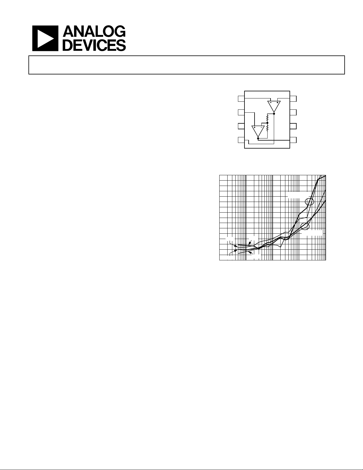
FUNCTIONAL BLOCK DIAGRAM
Figure 1.SOIC/LSCSP Pinout
GENERAL DESCRIPTION
The ADA4941-1 is a low power, low noise differential driver for
ADCs up to 18 bits in systems that are sensitive to power. The
ADA4941-1 is configured in an easy-to-use, single-ended-todifferential configuration and requires no external components
for a gain of 2 configuration. A resistive feedback network can
be added to achieve gains greater than 2. The ADA4941-1
provides essential benefits, such as low distortion and high
SNR, that are required for driving high resolution ADCs.
With a wide input voltage range (0 V to 3.9 V on a single 5 V
supply), rail-to-rail output, high input impedance, and a useradjustable gain, the ADA4941-1 is designed to drive singlesupply ADCs with differential inputs found in a variety of low
power applications, including battery-operated devices and
single-supply data acquisition systems.
Information furnished by Analog Devices is be lieved to be accurate and reliable. However, no
responsibility is assumed by Analog Devices for its use, nor for any infringements of patents or other
rights of third parties that may result from its use. Specifications subject to change without notice. No
license is granted by implication or otherwise under any patent or patent rights of Analog Devices.
The ADA4941-1 is ideal for driving the 16-bit and 18-bit
PulSAR® ADCs such as the AD7687, AD7690, and AD7691.
The ADA4941-1 is manufactured on ADI’s proprietary secondgeneration XFCB process, which enables the amplifier to
achieve 18-bit performance on low supply currents.
The ADA4941-1 is available in a small 8-lead LFCSP as well as a
standard 8-lead SOIC and is rated to work over the extended
industrial temperature range, −40°C to +125°C.
One Technology Way, P.O. Box 9106, Norwood, MA 02062-9106, U.S.A.
Tel: 781.329.4700
Figure 2. Distortion vs. Frequency at Various Output Amplitudes
www.analog.com

ADA4941-1
TABLE OF CONTENTS
Features .............................................................................................. 1
Output Voltage Noise ................................................................. 17
Applications ....................................................................................... 1
Functional Block Diagram .............................................................. 1
General Description ......................................................................... 1
Revision History ............................................................................... 2
Specifications ..................................................................................... 3
Absolute Maximum Ratings ............................................................ 6
Thermal Resistance ...................................................................... 6
ESD Caution .................................................................................. 6
Pin Configuration and Function Descriptions ............................. 7
Typical Performance Characteristics ............................................. 8
Theory of Operation ...................................................................... 15
Basic Operation .......................................................................... 15
DC Error Calculations ............................................................... 16
REVISION HISTORY
Frequency Response vs. Closed-Loop Gain ........................... 19
Applications ..................................................................................... 20
Overview ..................................................................................... 20
Using the REF Pin ...................................................................... 20
Internal Feedback Network Power Dissipation ...................... 20
Disable Feature ........................................................................... 20
Adding a 3-Pole, Sallen-Key Filter ........................................... 21
Driving the AD7687 ADC ........................................................ 22
Gain of −2 Configuration .......................................................... 22
Outline Dimensions ....................................................................... 23
Ordering Guide .......................................................................... 23
8/11—Rev. B to Rev. C
Change to Gain Error Drift Unit, Table 1...................................... 3
Change to Gain Error Drift Unit, Table 2...................................... 4
Change to Gain Error Drift Unit, Table 3...................................... 5
8/10—Rev. A to Rev. B
Added Caption to Figure 1 .............................................................. 1
Added Exposed Pad Notation to Figure 4 and Table 6 ................ 7
Added Exposed Pad Notation to Outline Dimensions ............. 23
Changes to Ordering Guide .......................................................... 23
3/09—Rev. 0 to Rev. A
Change to Gain Error Drift Parameter, Table 1 ............................ 3
Change to Gain Error Drift Parameter, Table 2 ............................ 4
Change to Gain Error Drift Parameter, Table 3 ............................ 5
Updated Outline Dimensions ....................................................... 23
4/06—Revision 0: Initial Version
Rev. C | Page 2 of 24

ADA4941-1
fC = 100 kHz, VO = 2 V p-p, HD2/HD3
−101/−98
dBc
Enabled, DIS = Low
≤1.0 V
SPECIFICATIONS
TA = 25°C, VS = 3 V, OUT+ connected to FB (G = 2), R
Table 1.
Parameter Conditions Min Typ Max Unit
DYNAMIC PERFORMANCE
−3 dB Bandwidth VO = 0.1 V p-p 21 30 MHz
VO = 2.0 V p-p 4.6 6.5 MHz
Overdrive Recovery Time +Recover/−Recovery 320/650 ns
Slew Rate VO = 2 V step 22 V/µs
Settling Time 0.005% VO = 2 V p-p step 300 ns
NOISE/DISTORTION PERFORMANCE
Harmonic Distortion fC = 40 kHz, VO = 2 V p-p, HD2/HD3 −116/−112 dBc
fC = 1 MHz, VO = 2 V p-p, HD2/HD3 −75/−71 dBc
RTO Voltage Noise f = 100 kHz 10.2 nV/√Hz
Input Current Noise f = 100 kHz 1.6 pA/√Hz
DC PERFORMANCE
Differential Output Offset Voltage 0.2 0.8 mV
Differential Input Offset Voltage Drift 1.0 µV/°C
Single-Ended Input Offset Voltage Amp A1 or Amp A2 0.1 0.4 mV
Single-Ended Input Offset Voltage Drift 0.3 µV/°C
Input Bias Current IN and REF 3 4.5 µA
Input Offset Current IN and REF 0.1 µA
Gain (+OUT − −OUT)/(IN − REF) 1.98 2.00 2.01 V/V
Gain Error −1 +1 %
Gain Error Drift 1 5 ppm/°C
INPUT CHARACTERISTICS
Input Resistance IN and REF 24 MΩ
Input Capacitance IN and REF 1.4 pF
Input Common-Mode Voltage Range 0.2 1.9 V
Common-Mode Rejection Ratio (CMRR) CMRR = V
OUTPUT CHARACTERISTICS
Output Voltage Swing Each single-ended output, G = 4 ±2.90 ±2.95 V
Output Current 25 mA
Capacitive Load Drive 20% overshoot, VO, dm = 200 mV p-p 20 pF
POWER SUPPLY
Operating Range 2.7 12 V
Quiescent Current 2.2 2.4 mA
Quiescent Current—Disable 10 16 µA
Power Supply Rejection Ratio (PSRR)
+PSRR PSRR = V
−PSRR 86 110 dB
DISABLE
DIS Input Voltage Disabled, DIS = High ≥1.5 V
= 1 kΩ, REF = 1.5 V, unless otherwise noted.
L, dm
OS, dm/VCM
OS, dm
, VREF = VIN, VCM = 0.2 V to 1.9 V, G = 4 81 105 dB
/ΔVS, G = 4 86 100 dB
DIS Input Current Disabled, DIS = High 5.5 8 µA
Enabled, DIS = Low 4 6 µA
Turn-On Time 0.7 µs
Turn-Off Time 30 µs
Rev. C | Page 3 of 24

ADA4941-1
Parameter
Conditions
Min
Typ
Max
Unit
RTO Voltage Noise
f = 100 kHz
10.2 nV/√Hz
Enabled, DIS = Low
4 6
µA
TA = 25°C, VS = 5 V, OUT+ connected to FB (G = 2), R
Table 2.
DYNAMIC PERFORMANCE
−3 dB Bandwidth VO = 0.1 V p-p 22 31 MHz
VO = 2.0 V p-p 4.9 7 MHz
Overdrive Recovery Time +Recover/−Recovery 200/600 ns
Slew Rate VO = 2 V step 24.5 V/µs
Settling Time 0.005% VO = 6 V p-p step 610 ns
NOISE/DISTORTION PERFORMANCE
Harmonic Distortion fC = 40 kHz, VO = 2 V p-p, HD2/HD3 −118/−119 dBc
fC = 100 kHz, VO = 2 V p-p, HD2/HD3 −110/−112 dBc
fC = 1 MHz, VO = 2 V p-p, HD2/HD3 −83/−73 dBc
Input Current Noise f = 100 kHz 1.6 pA/√Hz
DC PERFORMANCE
Differential Output Offset Voltage 0.2 0.8 mV
Differential Input Offset Voltage Drift 1.0 µV/°C
Single-Ended Input Offset Voltage Amp A1 or Amp A2 0.1 0.4 mV
Single-Ended Input Offset Voltage Drift 0.3 µV/°C
Input Bias Current IN and REF 3 4.5 µA
Input Offset Current IN and REF 0.1 µA
Gain (+OUT − −OUT)/(IN − REF) 1.98 2 2.01 V/V
Gain Error −1 +1 %
Gain Error Drift 1 5 ppm/°C
INPUT CHARACTERISTICS
Input Resistance IN and REF 24 MΩ
Input Capacitance IN and REF 1.4 pF
Input Common-Mode Voltage Range 0.2 3.9 V
Common-Mode Rejection Ratio (CMRR) C MRR = V
OUTPUT CHARACTERISTICS
Output Voltage Swing Each single-ended output, G = 4 ±4.85 ±4.93 V
Output Current 25 mA
Capacitive Load Drive 20% overshoot, VO, dm = 200 mV p-p 20 pF
POWER SUPPLY
Operating Range 2.7 12 V
Quiescent Current 2.3 2.6 mA
Quiescent Current—Disable 12 20 µA
Power Supply Rejection Ratio (PSRR)
+PSRR PSRR = V
−PSRR 87 110 dB
DISABLE
DIS Input Voltage Disabled, DIS = High ≥1.5 V
Enabled, DIS = Low ≤1.0 V
DIS Input Current Disabled, DIS = High 5.5 8 µA
= 1 kΩ, REF = 2.5 V, unless otherwise noted.
L, dm
OS, dm/VCM
OS, dm
, VREF = VIN, VCM = 0.2 V to 3.9 V, G = 4 84 106 dB
/ΔVS, G = 4 87 100 dB
Turn-On Time 0.7 µs
Turn-Off Time 30 µs
Rev. C | Page 4 of 24

ADA4941-1
Parameter
Conditions
Min
Typ
Max
Unit
RTO Voltage Noise
f = 100 kHz
10.2 nV/√Hz
Enabled, DIS = Low
≤ −4
V
TA = 25°C, VS = ±5 V, OUT+ connected to FB (G = 2), R
Table 3.
DYNAMIC PERFORMANCE
−3 dB Bandwidth VO = 0.1 V p-p 23 32 MHz
VO = 2.0 V p-p 5.2 7.5 MHz
Overdrive Recovery Time +Recover/−Recovery 200/650 ns
Slew Rate VO = 2 V step 26 V/µs
Settling Time 0.005% VO = 12 V p-p step 980 ns
NOISE/DISTORTION PERFORMANCE
Harmonic Distortion fC = 40 kHz, VO = 2 V p-p, HD2/HD3 −118/−119 dBc
fC = 100 kHz, VO = 2 V p-p, HD2/HD3 −109/−112 dBc
fC = 1 MHz, VO = 2 V p-p, HD2/HD3 −84/−75 dBc
Input Current Noise f = 100 kHz 1.6 pA/√Hz
DC PERFORMANCE
Differential Output Offset Voltage 0.2 0.8 mV
Differential Input Offset Voltage Drift 1.0 µV/°C
Single-Ended Input Offset Voltage Amp A1 or Amp A2 0.1 0.4 mV
Single-Ended Input Offset Voltage Drift 0.3 µV/°C
Input Bias Current IN and REF 3 4.5 µA
Input Offset Current IN and REF 0.1 µA
Gain (+OUT − −OUT)/(IN − REF) 1.98 2 2.01 V/V
Gain Error −1 +1 %
Gain Error Drift 1 5 ppm/°C
INPUT CHARACTERISTICS
Input Resistance IN and REF 24 MΩ
Input Capacitance IN and REF 1.4 pF
Input Common-Mode Voltage Range −4.8 +3.9 V
Common-Mode Rejection Ratio (CMRR) CMRR = V
V
CM
OUTPUT CHARACTERISTICS
Output Voltage Swing Each single-ended output, G = 4 VS − 0.25 VS ± 0.14 V
Output Current 25 mA
Capacitive Load Drive 20% overshoot, VO, dm = 200 mV p-p 20 pF
POWER SUPPLY
Operating Range 2.7 12 V
Quiescent Current 2.5 2.7 mA
Quiescent Current—Disable 15 26 µA
Power Supply Rejection Ratio (PSRR)
+PSRR PSRR = V
−PSRR 87 110 dB
DISABLE
DIS Input Voltage Disabled, DIS = High ≥ −3 V
= 1 kΩ, REF = 0 V, unless otherwise noted.
L, dm
OS, dm/VCM
, VREF = VIN,
= −4.8 V to +3.9 V, G = 4
/ΔVS, G = 4 87 100 dB
OS, dm
85 105 dB
DIS Input Current Disabled, DIS = High 7 10 µA
Enabled, DIS = Low 4 6 µA
Turn-On Time 0.7 µs
Turn-Off Time 30 µs
Rev. C | Page 5 of 24
ADA4941-1
2.5
0
–40 120
AMBIENT T E M P E RATURE (°C)
MAXIMUM POWER DISSIPATION (W)
2.0
1.5
1.0
0.5
–20 0 20 40 60 80 100
LFCSP
SOIC
05704-002
human body and test equipment and can discharge without detection. Although this product features
subjected to high energy
electrostatic discharges. Therefore, proper ESD precautions are recommended to avoid performance
ABSOLUTE MAXIMUM RATINGS
Table 4.
Parameter Rating
Supply Voltage 12 V
Power Dissipation See Figure 3
Storage Temperature Range −65°C to +125°C
Operating Temperature Range −40°C to +85°C
Lead Temperature (Soldering 10 sec) 300°C
Junction Temperature 150°C
Stresses above those listed under Absolute Maximum Ratings
may cause permanent damage to the device. This is a stress
rating only; functional operation of the device at these or any
other conditions above those indicated in the operational
section of this specification is not implied. Exposure to absolute
maximum rating conditions for extended periods may affect
device reliability.
THERMAL RESISTANCE
θJA is specified for the worst-case conditions, that is, θJA is
specified for a device soldered in the circuit board with its
exposed paddle soldered to a pad (if applicable) on the PCB
surface that is thermally connected to a copper plane, with zero
airflow.
Table 5. Thermal Resistance
Package Type θJA θJC Unit
8-Lead SOIC on 4-Layer Board 126 28
8-Lead LFCSP with EP on 4-Layer Board 83 19
Maximum Power Dissipation
The maximum safe power dissipation in the ADA4941-1
package is limited by the associated rise in junction temperature
(T
) on the die. At approximately 150°C, which is the glass
J
transition temperature, the plastic changes its properties. Even
temporarily exceeding this temperature limit can change the
stresses that the package exerts on the die, permanently shifting
the parametric performance of the ADA4941-1. Exceeding a
junction temperature of 150°C for an extended period can
result in changes in the silicon devices potentially causing
failure.
°C/W
°C/W
The power dissipated in the package (P
) is the sum of the
D
quiescent power dissipation and the power dissipated in the
package due to the load drive for all outputs. The quiescent
power is the voltage between the supply pins (V
quiescent current (I
). The power dissipated due to the load
S
) times the
S
drive depends upon the particular application. For each output,
the power due to load drive is calculated by multiplying the load
current by the associated voltage drop across the device. The
power dissipated due to all of the loads is equal to the sum of
the power dissipation due to each individual load. RMS voltages
and currents must be used in these calculations.
Airflow increases heat dissipation, effectively reducing θ
JA
. In
addition, more metal directly in contact with the package leads
from metal traces, through holes, ground, and power planes
reduces the θ
. The exposed paddle on the underside of the
JA
package must be soldered to a pad on the PCB surface that is
thermally connected to a copper plane to achieve the specified θ
.
JA
Figure 3 shows the maximum safe power dissipation in the
packages vs. the ambient temperature for the 8-lead SOIC
(126°C/W) and for the 8-lead LFCSP (83°C/W) on a JEDEC
standard 4-layer board. The LFCSP must have its underside
paddle soldered to a pad that is thermally connected to a PCB
plane. θ
Figure 3. Maximum Power Dissipation vs. Temperature for a 4-Layer Board
values are approximations.
JA
ESD CAUTION
ESD (electrostatic discharge) sensitive device. Electrostatic charges as high as 4000 V readily accumulate on
the
proprietary ESD protection circuitry, permanent damage may occur on devices
degradation or loss of functionality.
Rev. C | Page 6 of 24
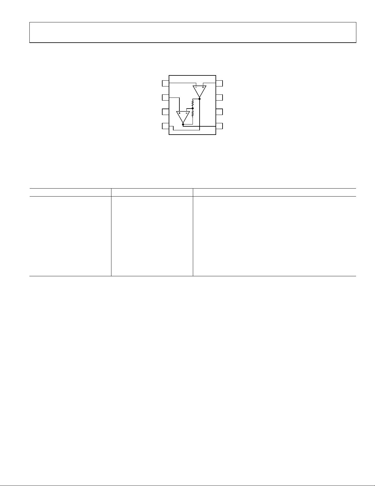
ADA4941-1
DIS
4
3
2
1
IN
OUT–OUT+
NOTES
1. THE EXPOSED PAD IS NOT ELECTRICALLY CONNECTED TO THE DEVICE.
IT IS TYPICALLY SOLDERED TO G ROUND OR A POWER PLANE ON THE PCB
THAT IS THERMALLY CONDUCTIVE.
V+
REF
FB
V–
7
8
5
6
05704-101
4
OUT+
Noninverting Output
5
OUT−
Inverting Output
PIN CONFIGURATION AND FUNCTION DESCRIPTIONS
Figure 4. Pin Configuration
Table 6. Pin Function Descriptions
Pin No. Mnemonic Description
1 FB Feedback Input
2 REF Reference Input
3 V+ Positive Power Supply
6 V− Negative Power Supply
7 DIS Disable
8 IN Input
EP (For LFCSP Only) Exposed Paddle. The exposed pad is not electrically connected to
the device. It is typically soldered to ground or a power plane on the
PCB that is thermally conductive.
Rev. C | Page 7 of 24
ADA4941-1
2
–16
–15
–14
–13
–12
1 1000
FREQUENCY (MHz)
NORMALIZED CLOSED-LOOP GAIN (dB)
1
0
–1
–2
–3
–11
–4
–5
–6
–7
–8
–9
–10
10 100
V
O, dm
= 0.1V p-p
VS = +3V
VS = +5V
V
S
= ±5V
05704-004
2
–16
–15
–14
–13
–12
1 1000
FREQUENCY (MHz)
NORMALIZED CLOSED-LOOP GAIN (dB)
1
0
–1
–2
–3
–11
–4
–5
–6
–7
–8
–9
–10
10 100
+25°C
–40°C
+85°C
V
O, dm
= 0.1V p-p
05704-005
2
–15
1 1000
FREQUENCY (MHz)
NORMALIZED CLOSED-LOOP GAIN (dB)
10 100
R
L, dm
= 1kΩ
R
L, dm
= 5kΩ
R
L, dm
= 500Ω
1
0
–1
–2
–3
–4
–5
–6
–7
–8
–9
–10
–11
–12
–13
–14
V
O, dm
= 0.1V p-p
05704-006
2
–16
–15
–14
–13
–12
0.1 100
FREQUENCY (MHz)
NORMALIZED CLOSED-LOOP GAIN (dB)
1
0
–1
–2
–3
–11
–4
–5
–6
–7
–8
–9
–10
1 10
VS = +3V
V
O, dm
= 2V p-p
VS = +5V
V
O, dm
= 6V p-p
VS = ±5V
V
O, dm
= 12V p-p
05704-007
2
–16
–15
–14
–13
–12
0.1 100
FREQUENCY (MHz)
NORMALIZED CLOSED-LOOP GAIN (dB)
1
0
–1
–2
–3
–11
–4
–5
–6
–7
–8
–9
–10
1 10
+25°C
–40°C
+85°C
V
O, dm
= 6V p-p
05704-008
2
–16
0.1 10
FREQUENCY (MHz)
NORMALIZED CLOSED-LOOP GAIN (dB)
R
L, dm
= 1kΩ
R
L, dm
= 5kΩ
R
L, dm
= 500Ω
V
O, dm
= 6V p-p
1
0
–1
–2
–3
–4
–5
–6
–7
–8
–9
–10
–11
–12
–13
–14
–15
1
05704-009
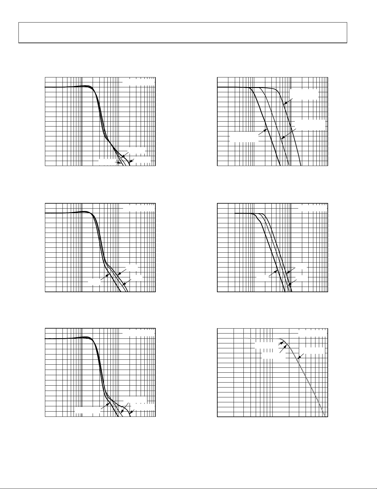
TYPICAL PERFORMANCE CHARACTERISTICS
Unless otherwise noted, VS = 5 V, R
= 1 kΩ, REF = 2.5 V, DIS = LOW, OUT+ directly connected to FB (G = 2), TA = 25°C.
L, dm
Figure 5. Small Signal Frequency Response for Various Power Supplies
Figure 6. Small Signal Frequency Response at Various Temperatures
Figure 8. Large Signal Frequency Response for Various Power Supplies
Figure 9. Large Signal Frequency Response at Various Temperatures
Figure 7. Small Signal Frequency Response for Various Resistive Loads
Figure 10. Large Signal Frequency Response for Various Resistive Loads
Rev. C | Page 8 of 24

ADA4941-1
2
–16
–15
–14
–13
–12
1 100
FREQUENCY (MHz)
NORMALIZED CLOSED-LOOP GAIN (dB)
1
0
–1
–2
–3
–11
–4
–5
–6
–7
–8
–9
–10
10
G = +4
G = +10
G = +2
G = –2
V
O, dm
= 0.1V p-p
05704-010
2
–16
–15
–14
–13
–12
1 10010 1000
FREQUENCY (MHz)
NORMALIZED CLOSED-LOOP GAIN (dB)
1
0
–1
–2
–3
–11
–4
–5
–6
–7
–8
–9
–10
CL = 0pF
CL = 20pF
V
O, dm
= 0.1V p-p
05704-011
2
–16
–15
–14
–13
–12
1 10 1000
FREQUENCY (MHz)
NORMALIZED CLOSED-LOOP GAIN (dB)
1
0
–1
–2
–3
–11
–4
–5
–6
–7
–8
–9
–10
VREF = 0.05V p-p
V
S
= +5V
VS = ±5V
VS = +3V
05704-012
2
–16
–15
–14
–13
–12
1 10 1000
FREQUENCY (MHz)
NORMALIZED CLOSED-LOOP GAIN (dB)
1
0
–1
–2
–3
–11
–4
–5
–6
–7
–8
–9
–10
100
G = +4
G = +10
G = +2
G = –2
V
O, dm
= 2V p-p
05704-013
2
–16
–15
–14
–13
–12
0.1 101 1000
FREQUENCY (MHz)
NORMALIZED GAIN (d B)
1
0
–1
–2
–3
–
11
–4
–5
–6
–7
–8
–9
–10
100
V
O, dm
= 2V p-p
V
O, dm
= 6V p-p
V
O, dm
= 0.1V p-p
05704-014
–70
–140
0.1 101 1000
FREQUENCY ( kHz )
DISTORTION (dBc)
100
05704-015
HD3
HD2
HD2
RL = 2kΩ
RL = 1kΩ
RL = 500Ω
V
O, dm
= 2V p-p
VREF = MIDSUPPLY
–80
–90
–100
–110
–120
–130
Figure 11. Small Signal Frequency Response for Various Gains
Figure 12. Small Signal Frequency Response for Various Capacitive Loads
Figure 14. Large Signal Frequency Response for Various Gains
Figure 15. Frequency Response for Various Output Amplitudes
Figure 13. REF Input Small Signal Frequency Response for Various Supplies
Figure 16. Distortion vs. Frequency for Various Loads
Rev. C | Page 9 of 24

ADA4941-1
–
–
–
–
–
65
–75
–85
–95
–105
HD3
DISTORTION (dBc)
–115
–125
–135
020
HD2
HD2
HD3
24681012141618
OUTPUT AMP LITUDE (V p -p)
VS = +5V
f
= 10kHz
VS = ±5VVS = +3V
HD3
HD2
05704-016
Figure 17. Distortion vs. Output Amplitude for Various Supplies (G = +2)
60
V
= 2V p-p
O, dm
–65
VREF = MIDSUP P L Y
–70
–75
–80
–85
–90
–95
–100
–105
–110
DISTORT ION (dBc)
–115
HD3
–120
–125
HD2
–130
–135
–140
0.1 101 1000
HD2
HD3
FREQUENCY (kHz)
100
VS = +3V
VS = +5V
VS =±5V
05704-017
Figure 18. Distortion vs. Frequency for Various Supplies
60
–65
–70
–75
–80
–85
–90
–95
–100
–105
–110
DISTORT ION (dBc)
–115
–120
HD3
–125
–130
–135
HD2
–140
0.1 101 1000
HD2
HD3
FREQUENCY (kHz)
VO = 6V p-p
VO = 2V p-p
100
05704-045
Figure 19. Distortion vs. Frequency at Various Output Amplitudes
65
–75
–85
DISTORTION (dBc)
–95
–105
–115
–125
–135
–145
VS = +3V
HD3
HD2
020
24681012141618
HD3
OUTPUT AMPLITUDE (V p-p)
DIFFERENTIAL G = –2
f
= 10kHz
VS = +5V VS = ±5V
HD3
05704-019
Figure 20. Distortion vs. Output Amplitude for Various Supplies (G = −2)
70
V
= 2V p-p
O, dm
VREF = MIDSUPPLY
–80
–90
–100
–110
DISTORT ION (dBc)
–120
HD3
–130
HD3 HD3
–140
0.1 101 1000
HD2
HD2
FREQUENCY (kHz)
100
G = –2
G = +2
G = +4
05704-020
Figure 21. Distortion vs. Frequency for Various Gains
–0.04
OUTPUT VOLTAGE (V)
–0.08
–0.12
0.12
0.08
0.04
0
CL =0pF
CL = 20pF
V
OUT
= 200mV p - p
50ns/DIV
05704-022
Figure 22. Small Signal Transient Response for Various Capacitive Loads
Rev. C | Page 10 of 24

ADA4941-1
0.12
–0.12
OUTPUT VOLTAGE (V)
50ns/DIV
V
OUT
= 200mV p-p
0.08
0.04
0
–0.04
–0.08
VS = +3V
VS = +5V OR VS = ±5V
05704-018
8
–8
AMPLITUDE (V)
VS = ±5V
V
O, dm
= 12V p-p
V
O, dm
2 × V
IN
ERROR = 2 × VIN – V
O, dm
6
4
2
0
–2
–4
–6
2.4
–2.4
ERROR (mV) 1 DI V = 0.005%
1.8
1.2
0.6
0
–0.6
–1.2
–1.8
1µs/DIV
05704-023
12
–12
10
8
6
4
2
0
–2
–4
–6
–8
–10
OUTPUT VOLTAGE (V)
1µs/DIV
INPUT × 2
OUTPUT
05704-024
8
–8
OUTPUT VOLTAGE (V)
200ns/DIV
V
S
= ±5V
V
O, dm
= 12V p-p
V
S
= ±2.5V
V
O, dm
= 6V p-p
V
S
= ±1.5V
V
O, dm
= 2V p-p
6
4
2
0
–2
–4
–6
05704-021
9
1
AMPLITUDE (V)
VS = +5V
V
O, dm
= 6V p-p
V
O, dm
2 × V
IN
ERROR = 2 × VIN – V
O, dm
8
7
6
5
4
3
2
1.2
–1.2
ERROR (mV) 1 DI V = 0.005%
0.9
0.6
0.3
0
–0.3
–0.6
–0.9
1µs/DIV
05704-026
8
–8
OUTPUT VOLTAGE (V)
1µs/DIV
6
4
2
0
–2
–4
–6
INPUT × 2
OUTPUT
05704-027
Figure 23. Small Signal Transient Response for Various Supplies
Figure 24. Settling Time (0.005%), V
= ±5 V
S
Figure 26. Large Signal Transient Response for Various Supplies
Figure 27. Settling Time (0.005%), V
= +5 V
S
Figure 25. Input Overdrive Recovery, V
= ±5 V
S
Rev. C | Page 11 of 24
Figure 28. Input Overdrive Recovery, V
= +5 V
S

ADA4941-1
0
–110
0.001 1000
FREQUENCY (MHz)
PSRR (dB)
–10
–20
–30
–40
–50
–60
–70
–80
–90
–100
0.01 0.1 1 10 100
+PSRR
–PSRR
05704-028
3.5
1.0
–40 120
TEMPERATURE (°C)
POWER SUP P LY CURRENT (mA)
VS = ±5V
V
S
= +5V
VPD = V
S–
V
S
= +3V
3.0
2.5
2.0
1.5
–20 0 20 40 60 80 100
05704-029
150
0
–40 120
TEMPERATURE (°C)
DIFFERENTIAL OUTPUT OFFSET (µV)
–20 0 20 40 60 80 100
05704-030
125
100
75
50
25
VOS_A1 10V
V
OS
_A2 = 3V
VOS_A1 = 3V
VOS_A2 = 5V
VOS_A1 = 5V
V
OS
_A2 = 10V
0.18
0.16
0.14
0.12
0.10
0.08
0.06
0.04
–40 120
TEMPERATURE (°C)
OUTPUT SATURATION VOLTAGE
WITH RESPECT TO RAIL (V)
–20 0 20 40 60 80
100
05704-031
±5V SUPPLIES, POSITIVE RAIL
+5V SUPPLIES, POSITIVE RAIL
±5V SUPPLIES, NEGATIVE RAIL
+5V SUPPLIES, NEGATIVE RAIL
+3V SUPPLIES, POSITIVE RAIL
+3V SUPPLIES, NEGATIVE RAIL
2.5
–0.5
0.6 2.0
DISABLE INPUT VOLTAGE WITH RESPECT TO V
S–
(V)
SUPPLY CURRENT (mA)
ICC@ VS = ±5V
ICC@ VS = +5V
ICC@ VS = +3V
2.0
1.5
1.0
0.5
0
0.8 1.0 1.2 1.4 1.6 1.8
05704-032
140
0
–200
–180
–160
–140
–120
–100
–80
–60
–40
–20
0
204060
80
100
120
140
160
180
200
OFFSET VOLTAGE (µV)
FREQUENCY
120
100
80
60
40
20
V
OS
1
MEAN = –8µV
STD. DEV = 47µV
V
OS
2
MEAN = 11µV
STD. DEV = 20µV
NO. OF UNITS = 611
05704-033
Figure 29. Power Supply Rejection Ratio vs. Frequency
Figure 30. Power Supply Current vs. Temperature
Figure 32. Output Saturation Voltage vs. Temperature
Figure 33. Power Supply Current vs. Disable Voltage
Figure 31. Differential Output Offset Voltage vs. Temperature
Figure 34. Differential Output Offset Distribution
Rev. C | Page 12 of 24

ADA4941-1
100
1
1 100M
FREQUENCY ( Hz )
DIFFERENTIAL OUTPUT VOLTAGE NOISE (nV/√Hz)
10
10 100 1k 10k 100k 1M 10M
05704-034
2.65
2.35
–40 125
TEMPERATURE (°C)
INPUT BIAS CURRE NT (µA)
VS = ±5V
VS = +5V
VS = +3V
2.60
2.55
2.50
2.45
2.40
–25 –10 5 20 35 50 65 80 95 110
05704-035
3.3
2.7
–40 120
TEMPERATURE (°C)
REFERENCE BI AS CURRE NT (µA)
–20 0 20 40 60 80 100
05704-036
3.2
3.1
3.0
2.9
2.8
REFERENCE I
BIAS
= 5V
REFERENCE I
BIAS
= 3V
REFERENCE I
BIAS
= 10V
28
0
1
1M
FREQUENCY ( Hz )
INPUT CURRENT NOISE (pA/ √Hz )
26
24
22
20
18
16
14
12
10
8
6
4
2
10 100 1k 10k 100k
05704-037
3.5
1.5
–0.5
10.0
INPUT VOLTAGE WITH RESPECT TO V
S–
(V)
INPUT BIAS CURRE NT (µA)
05704-038
3.0
2.5
2.0
0
0.5
1.0
1.5
2.0
2.5
3.0
3.5
4.0
4.5
5.0
5.5
6.0
6.5
7.0
7.5
8.0
8.5
9.0
9.5
V
S
= ±5V
V
S
= +5V
V
S
= +3V
4.0
2.0
0 10.0
REFERENCE INPUT VOLTAGE WITH RESPECT TO V
S–
(V)
REFERENCE I NP UT BIAS CURRENT (µ A)
05704-039
3.5
3.0
2.5
0.5
1.0
1.5
2.0
2.5
3.0
3.5
4.0
4.5
5.0
5.5
6.0
6.5
7.0
7.5
8.0
8.5
9.0
9.5
VS = ±5V
VREF = VI N
VS = +5V
VS = +3V
Figure 35. Differential Output Voltage Noise vs. Frequency
Figure 36. Input Bias Current vs. Temperature for Various Supplies
Figure 38. Input Current Noise vs. Frequency
Figure 39. Input Bias Current vs. Input Voltage
Figure 37. REF Input Bias Current vs. Temperature
Figure 40. REF Input Bias Current vs. REF Input Voltage
Rev. C | Page 13 of 24
ADA4941-1
10
0
–40 120
TEMPERATURE (°C)
DISABLED SUP P LY CURRENT (µA)
–20 0 20 40 60 80 100
05704-040
8
6
4
2
G = 4
R
F
= 1kΩ
R
L
= ∞
DIS = HIGH
V
S
= ±5V
VS = +5V
V
S
= +3V
500mV/DIV
40µs/DIV
V
PD
V
O, dm
05704-041
–40
–110
0.1 1000
FREQUENCY (MHz)
ISOLATION (dB)
–50
–60
–70
–80
–90
–100
1 10 100
VIN = 50mV p-p
05704-042
14
0
0 10
DISABLE INPUT VOLTAGE WITH RESPECT TO V
S–
(V)
DISABLE I NP UT CURRENT (µA)
12
10
8
6
4
2
1 2 3 4 5 6 7 8 9
V
S
= ±5V
05704-043
500mV/DIV
40µs/DIV
V
PD
V
O, dm
05704-044
100
0.0001
0.001 100
FREQUENCY (MHz)
IMPEDANCE (Ω)
VOP
VON
10
1
0.1
0.01
0.001
0.01 0.1 1 10
05704-025
Figure 41. Disable Supply Current vs. Temperature for Various Supplies
Figure 42. Disable Assert Time
Figure 44. Disable Input Current vs. Disable Input Voltage
Figure 45. Disable Deassert Time
Figure 43. Disabled Input-to-Output Isolation vs. Frequency
Figure 46. Single-Ended Output Impedance vs. Frequency
Rev. C | Page 14 of 24

ADA4941-1
1kΩ
1kΩ
R
G
R
F
R
F
|| R
G
500Ω
A2
A1
REF
IN
VREF
2
8
4
5
FB
OUT+
+
–
VOP
1
OUT–
+
–
VON
VIN
VG
05704-052
−
+=
G
F
G
F
R
R
VG
R
R
VINVOP 1
)(21 VREF
R
R
VG
R
R
VINVON
G
F
G
F
+
+
+−=
)(221)(2
,
VREF
R
R
VG
R
R
VINVONVOP
dmV
G
F
G
F
O
−
−
+=−
=
VREF
VONVOP
cmV
O
=
+
=
2
,
1kΩ
1kΩ
4.99kΩ
1kΩ
825Ω
500Ω
A2
A1
REF
IN
2
8
4
5
FB
+5V
–5V
V
S+
V
S–
OUT+
+
–
VOP
1
3
6
OUT–
+
–
VON
VIN
05704-053
1kΩ
1kΩ
500Ω
A2
A1
REF
IN
2
8
4
5
FB
+5V
V
S+
V
S–
OUT+
+
–
VOP
1
3
6
OUT–
+
–
VON
+2.5V
VIN
05704-054
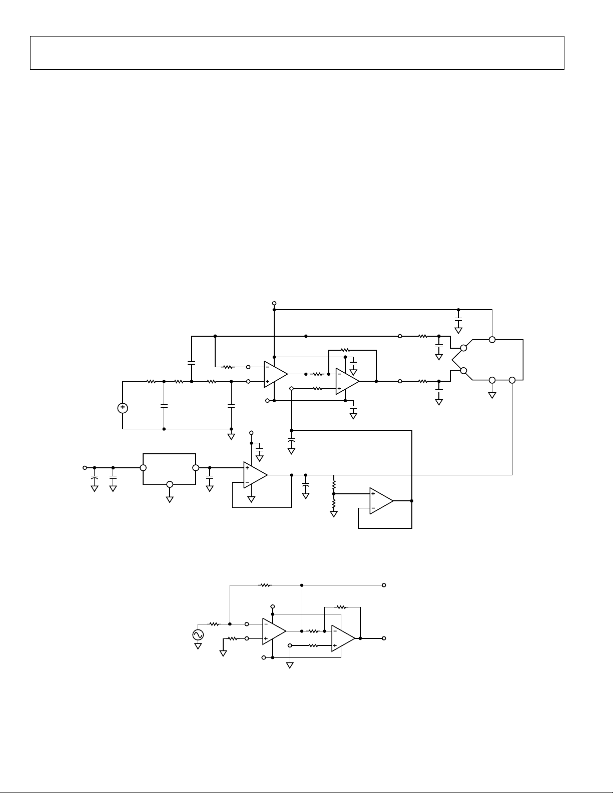
THEORY OF OPERATION
The ADA4941-1 is a low power, single-ended input, differential
output amplifier optimized for driving high resolution ADCs.
Figure 47 illustrates how the ADA4941-1 is typically connected.
The amplifier is composed of an uncommitted amplifier, A1,
driving a precision inverter, A2. The negative input of A1 is
brought out to Pin 1 (FB), allowing for user-programmable
gain. The inverting op amp, A2, provides accurate inversion of
the output of A1, VOP, producing the output signal VON.
(4)
When R
= 0 and RG is removed, Equation 3 simplifies to the
F
following:
V
, dm = 2(VIN) − 2(VREF) (5)
O
(3)
Figure 47. Basic Connections (Power Supplies Not Shown)
The voltage applied to the REF pin appears as the output
common-mode voltage. Note that the voltage applied to the
REF pin does not affect the voltage at the OUT+ pin. Because of
this, a differential offset can exist between the outputs, while the
desired output common-mode voltage is present. For example,
when VOP = 3.5 V and VON = 1.5 V, the output commonmode voltage is equal to 2.5 V, just as it is when both outputs
are at 2.5 V. In the first case, the differential voltage (or offset) is
2.0 V, and in the latter case, the differential voltage is 0 V. When
calculating output voltages, both differential and common-mode
voltages must be considered at the same time to avoid undesired
differential offsets.
BASIC OPERATION
In Figure 47, RG and RF form the external gain-setting network.
VG and VREF are externally applied voltages. V
as the output common-mode voltage and V
the differential-mode output voltage. The following equations
can be derived from Figure 47:
(1)
, cm is defined
O
, dm is defined as
O
Figure 48. Dual Supply, G = 2.4, Single-Ended-to-Differential Amplifier
Figure 48 shows an example of a dual-supply connection. In this
example, VG and VREF are set to 0 V, and the external R
R
network provides a noninverting gain of 1.2 in A1. This
G
and
F
example takes full advantage of the rail-to-rail output stage.
The gain equation is
VOP − VON = 2.4(VIN) (6)
The in-series, 825 Ω resistor combined with Pin 8 compensates
for the voltage error generated by the input offset current of A1.
The linear output range of both A1 and A2 extends to within
200 mV of each supply rail, which allows a peak-to-peak
differential output voltage of 19.2 V on ±5 V supplies.
(2)
Figure 49. Single +5V Supply, G=2 Single-Ended-to-Differential Amplifier
Figure 49 shows a single 5 V supply connection with A1 used as
a unity gain follower. The 2.5 V at the REF pin sets the output
common-mode voltage to 2.5 V. The transfer function is then
Rev. C | Page 15 of 24
VOP − VON = 2(VIN) − 5 V (7)

ADA4941-1
1kΩ
1kΩ
665Ω
1.02kΩ
402Ω
500Ω
A2
A1
REF
IN
2
8
4
5
FB
+5V
V
S+
V
S–
OUT+
+
–
VOP
1
3
OUT–
+
–
VON
VIN
+2.5V
6
05704-055
1kΩ
1kΩ
R
G
R
F
RS–IN
I
BP–
A2
I
BN–
A2
V
OS–
A1
500Ω
A2
A1
REF
IN
2
8
4
5
FB
OUT+
+
–
VOP
1
OUT–
+
–
VON
V
OS–
A2
RS–REF
I
BP–
A1
I
BN–
A1
05704-056
=
[ ]
)||()(1
G
F
S
F
OSOS
G
F
RRRRI_A1V
R
R
VOP_error =+
+=
VOL
SCM
OSOS
A
VOUT
PSRR
V
CMRR
V
_nomVV
Δ
ΔΔ
+++=
In this case, the linear output voltage is limited by A1. On the
low end, the output of A1 starts to saturate and show degraded
linearity when VOP approaches 200 mV. On the high end, the
input of A1 becomes saturated and exhibits degraded linearity
when VIN moves beyond 4 V (within 1 V of VCC). This limits
the linear differential output voltage in the circuit shown in
Figure 49 to about 7.6 V p-p.
Figure 50. 5 V Supply, G = 5, Single-Ended-to-Differential Amplifier
Figure 50 shows a single 5 V supply connection for G = 5. The
R
and RG network sets the gain of A1 to 2.5, and the 2.5 V at
F
the REF input provides a centered 2.5 V output common-mode
voltage. The transfer function is then
VOP − VON = 5(VIN) − 5 V (8)
The output range limits of A1 and A2 limit the differential
output voltage of the circuit shown in Figure 50 to approximately
8.4 V p-p.
When using data from the Specifications tables, it is often more
expedient to use input offset current in place of the individual
input bias currents when calculating errors. Input offset current
is defined as the magnitude of the difference between the two
input bias currents. Using this definition, each input bias
current can be expressed in terms of the average of the two
input bias currents, I
I
= IB ± IOS/2. DC errors are minimized when RS = RF || RG. In
B P, N
, and the input offset current, IOS, as
B
this case, Equation 9 is reduced to
Equation 10 expresses the dc voltage error present at the VON
output.
VON_error = −(VOP_error) + 2[V
(I
_A2)(RS_REF + 500)] + 1000(IBN_A2) (10)
BP
_A2 −
OS
The internal 500 Ω resistor is provided on-chip to minimize dc
errors due to the input offset current in A2. The minimum
error is achieved when R
_REF = 0 Ω. In this case, Equation 10
S
is reduced to
VON_error =
−(VOP_error) + 2[V
The differential output voltage error V
_A2] + (IOS)1000 (RS_REF = 0 Ω)
OS
_error, dm, is the
O
difference between VOP_error and VON_error:
V
_error, dm = VOP_error − VON_error (11)
O
DC ERROR CALCULATIONS
Figure 51. DC Error Sources
Figure 51 shows the major contributions to the dc output
voltage error. For each output, the total error voltage can be
calculated using familiar op amp concepts. Equation 9 expresses
the dc voltage error present at the VOP output.
VOP_error
+
R
F
[ ]
OS
R
G
The output offset voltage of each amplifier in the ADA4941-1
also includes the effects of finite common-mode rejection ratio
(CMRR), power supply rejection ratio (PSRR), and dc openloop gain (A
VOL
).
(12)
where:
_nom is the nominal output offset voltage without including
V
OS
the effects of CMRR, PSRR, and A
VOL
.
Δ indicates the change in conditions from nominal.
is the input common-mode voltage (for A1, the voltage at
V
CM
IN, and for A2, the voltage at REF).
V
is the power supply voltage.
S
VOUT is either op amp output.
(9)
R_A1I_INR_A1I_A1V
)())((1 +−
FBP
Rev. C | Page 16 of 24
BP
S

ADA4941-1
VOS_A1
0.1 mV
+0.25 mV
−0.25 mV
+0.5 mV
1kΩ
1kΩ
R
G
R
F
R
S
ip–A2
in
–
A2
vn
–
A1
500Ω
A2
A1
REF
IN
2
8
4
5
FB
OUT+
+
–
VOP
1
OUT–
+
–
VON
vn
–
A2
RS–REF
ip–A1
in
–
A1
05704-057
√4kT (1kΩ)
√4kT (1kΩ)
√4kT (500Ω)
√4kT (RS–REF)√4kTR
S
√4kTR
G
√4kTR
F
[ ]
[ ]
2
2
2
2
2
2
2
2
_41
24242
_2)_(1
2)_(12
_,
nVONkTR
R
R
R
R
kTRkTR
RA1inRA1ip
R
R
A1vn
R
R
ndmV
S
G
F
G
F
G
F
F
S
G
F
G
F
O
+
×
+
×+
×+
+×+
××
+
×+
×
+
=
( )
[ ]
[ ]
)(16(500)16(1000)8
)_(1000)_500)(_(4
4
22
22
_REFRkTkTkT
A2inREFRA2ip
vn_A2VON_n
S
S
++
+++
+=
Tabl e 7, Table 8, and Table 9 show typical error budgets for the
circuits shown in Figure 48, Figure 49, and Figure 50.
R
= 1.0 kΩ, RG = 4.99 kΩ, RS_IN = 825 Ω, RS_REF = 0 Ω
F
Table 7. Output Voltage Error Budget for G = 2.4 Amplifier
Shown in Figure 48
Error
Source
Typical
Value VOP_error VON_error V
_dm_error
O
VOS_A1 0.1 mV +0.12 mV −0.12 mV +0.24 mV
IBP_A1 3 µA +2.48 mV −2.48 mV −4.96 mV
IBN_A1 3 µA −2.48 mV +2.48 mV +4.96 mV
VOS_A2 0.1 mV 0 mV +0.2 mV +0.2 mV
Total VO_error, dm = 0.44 mV
RF = 0 Ω, RG = ∞, RS_IN = 0 Ω, RS_REF = 0 Ω
Table 8. Output Voltage Error Budget for Amplifier Shown
in Figure 49
Error
Source
Typical
Value
VOP_error VON_error V
_dm_error
O
VOS_A1 0.1 mV +0.1 mV −0.1 mV +0.2 mV
IBP_A1 3 µA +2.48 mV −2.48 mV −4.96 mV
IBN_A1 3 µA −2.48 mV +2.48 mV +4.96 mV
VOS_A2 0.1 mV 0 mV +0.2 mV +0.2 mV
Total VO_error, dm = 0.4 mV
RF = 1.02 kΩ, RG = 665 Ω, RS_IN = 402 Ω, RS_REF = 0 Ω
Table 9. Output Voltage Error Budget for G = 5 Amplifier
Shown in Figure 50
Error
Source
Typical
Value VOP_error VON_error V
_dm_error
O
IBP_A1 3 µA +1.21 mV −1.21 mV −2.4 mV
IBN_A1 3 µA −1.21 mV +1.21 mV +2.4 mV
VOS_A2 0.1 mV 0 mV +0.2 mV +0.2 mV
Total VO_error, dm = 0.7 mV
OUTPUT VOLTAGE NOISE
Figure 52 shows the major contributors to the ADA4941-1
differential output voltage noise. The differential output noise
mean-square voltage equals the sum of twice the noise meansquare voltage contributions from the noninverting channel
(A1), plus the noise mean-square voltage terms associated with
the inverting channel (A2).
(13)
2
where
VON_n
is calculated as
(14)
where:
vn_A1
and
vn_A2
are the input voltage noises of A1 and A2,
each equal to 2.1 nV/√Hz.
in_A1, in_A2, ip_A1
, and
ip_A2
are amplifier input current
noise terms, each equal to 1 pA/√Hz.
RS, RF, and RG are the external source, feedback, and gain
resistors, respectively.
kT is Boltzmann’s constant times absolute temperature, equal to
-21
4.2 x 10
R
S
W-s at room temperature.
_REF is any source resistance at the REF pin.
When A1 is used as a unity gain follower, the output voltage
noise spectral density is at its minimum, 10 nV/√Hz. Higher
voltage gains have higher output voltage noise.
Figure 52. Noise Sources
Tabl e 10, Table 11, and Table 12 show the noise contributions
and output voltage noise for the circuits in Figure 48, Figure 49,
and Figure 50.
Rev. C | Page 17 of 24

ADA4941-1
Noise Source
Typical Value
VOP Contribution (nV√Hz)
VON Contribution (nV√Hz)
VO, dm Contribution (nV√Hz)
√
9 nV/√Hz
1.8
1.8
3.6
Table 10. Output Voltage Noise, G = 2.4 Differential Amplifier Shown in Figure 48
2.1 nV/√Hz 2.5 2.5 5
vn_A1
1 pA/√Hz 1 1 2
ip_A1
1 pA/√Hz 1 1 2
in_A1
√
4 nV/√Hz 4 4 8
4 kTR
F
4 kTR
G
√
3.6 nV/√Hz 4.4 4.4 8.8
4 kTR
S
vn_inverter
√RS_REF
ip_A2 × RS_REF
RF = 1.0 kΩ, RG = 4.99 kΩ, RS = 825 Ω, RS_REF = 0 Ω.
9.2 nV/√Hz 0 9.2 9.2
0 0 0 0
0 0 0 0
Totals 6.8 11.4 16.5
vn_inverter
= noise contributions from A2 and its associated internal 1 kΩ feedback resistors and 500 Ω offset current balancing resistor.
Table 11. Output Voltage Noise, G = 2 Differential Amplifier Shown in Figure 49
Noise Source Typical Value VOP Contribution (nV√Hz) VON Contribution (nV√Hz) VO, dm Contribution (nV√Hz)
2.1 nV/√Hz 2.1 2.1 4.2
vn_A1
0 0 0 0
ip_A1
0 0 0 0
in_A1
√
0 0 0 0
4 kTR
F
√
0 0 0 0
4 kTR
G
√
0 0 0 0
4 kTR
S
vn_inverter
√RS_REF
ip_A2 × RS_REF
9.2 nV/√Hz 0 9.2 9.2
0 0 0 0
0 0 0 0
Totals 2.1 9.4 10
RF = 0 Ω, RG = ∞, RS = 0 Ω, RS_REF = 0 Ω.
Table 12. Output Voltage Noise, G = 5 Differential Amplifier Shown in Figure 50
Noise Source Typical Value VOP Contribution (nV√Hz) VON Contribution (nV√Hz) VO, dm Contribution (nV√Hz)
2.1 nV/√Hz 5.25 5.25 10.5
vn_A1
1 pA/√Hz 1 1 2
ip_A1
1 pA/√Hz 1 1 2
in_A1
√
4 nV/√Hz 4 4 8
4 kTR
F
√
3.26 nV/√Hz 4.9 4.9 9.8
4 kTR
G
√
2.54 nV/√Hz 6.54 6.54 13.1
4 kTR
S
vn_inverter
√RS_REF
ip_A2 × RS_REF
Totals 10.7 14.1 23.1
9.2 nV/√Hz 0 9.2 9.2
0 0 0 0
0 0 0 0
RF = 1.02 kΩ, RG = 665 Ω, RS = 402 Ω, RS_REF = 0 Ω.
Rev. C | Page 18 of 24

ADA4941-1
100
0
0.001 100
FREQUENCY (MHz)
OPEN-LOOP GAIN (dB)
05704-062
80
60
40
20
0.01 0.1 1 10
fcr = 50MHz
×
+
+
×
+×=
fcr
f
R
RR
R
R
VIN_A1V
G
G
F
G
F
O
1
1
1
+
×−=
×
+
×−=
MHz25
1
1
MHz50
2
1
1
2_
f
VOP
f
VINAV
O
+
MHz25
1
1
f
+
+
×
×
+
+
×
+×=
MHz25
1
1
1
MHz50
1
1
1
f
f
R
RR
R
R
VIN, dmV
G
G
F
G
F
O
+×
×
+
+
×
+=
MHz25
1
MHz50
1
2
1,
ff
R
RR
R
R
VINdmV
G
G
F
G
F
O
FREQUENCY RESPONSE VS. CLOSED-LOOP GAIN
The operational amplifiers used in the ADA4941-1 are voltage
feedback with an open-loop frequency response that can be
approximated with the integrator response, as shown in Figure 53.
The inverting amplifier A2 has a fixed feedback network. The
transfer function is approximately
A1’s frequency response depends on the external feedback
network as indicated by Equation 15. The overall differential
output voltage is therefore
V
, dm = VOP − VON = VOP + VOP ×
O
(18)
(17)
Figure 53. ADA4941-1 Op Amp Open-Loop Gain vs. Frequency
For each amplifier, the frequency response can be approximated
(19)
by the following equations:
(15)
Multiplying the terms and neglecting negligible terms leads to
the following approximation:
(Noninverting Response)
−
R
F
×=
VIN_A2V
O
×
R
G
1
1
+
RR
F
+
G
R
G
(16)
f
×
fcr
(20)
(Inverting Response)
is the gain-bandwidth frequency of the amplifier (where the
f
CR
open-loop gain shown in Figure 53 equals 1). f
for both
CR
amplifiers is about 50 MHz.
There are two poles in this transfer function, and the lower
frequency pole limits the bandwidth of the differential
amplifier. If VOP is shorted to IN− (A1 is a unity gain follower),
the 25 MHz closed-loop bandwidth of the inverting channel
limits the overall bandwidth. When A1 is operating with higher
noise gains, the bandwidth is limited by A1’s closed-loop
bandwidth, which is inversely proportional to the noise gain
(1 + R
). For instance, if the external feedback network
F/RG
provides a noise gain of 10, the bandwidth drops to 5 MHz.
Rev. C | Page 19 of 24

ADA4941-1
APPLICATIONS
OVERVIEW
The ADA4941-1 is an adjustable-gain, single-ended-to-differential
voltage amplifier, optimized for driving high resolution ADCs.
Single-ended-to-differential gain is controlled by one feedback
network, comprised of two external resistors: R
and RG.
F
USING THE REF PIN
The REF pin sets the output base line in the inverting path and
is used as a reference for the input signal. In most applications,
the REF pin is set to the input signal midswing level, which in
many cases is also midsupply. For bipolar signals and dual
power supplies, REF is generally set to ground. In single-supply
applications, setting REF to the input signal midswing level
provides optimal output dynamic range performance with
minimum differential offset. Note that the REF input only
affects the inverting signal path or VON.
The best use of the REF pin can be further illustrated by
considering a single-supply case with a 10 V power supply and
an input signal that varies between 2 V and 7 V. This is a case
where the midswing level of the input signal is not at midsupply
but is at 4.5 V. Setting the REF input at 4.5 V and neglecting
offsets, Equation 21 and Equation 22 are used to calculate the
results. When the input signal is at its midpoint of 4.5 V,
OUT+ is at 4.5 V, as is VON. This can be considered as a base
line state where the differential output voltage is 0. When the
input increases to 7 V, VOP tracks the input to 7 V, and VON
decreases to 2 V. This can be viewed as a positive peak signal
where the differential output voltage equals 5 V. When the input
signal decreases to 2 V, VOP again tracks to 2 V, and VON
increases to 7 V. This can be viewed as a negative peak signal
where the differential output voltage equals −5 V. The resulting
differential output voltage is 10 V p-p.
Most applications require a differential output signal with the
same dc common-mode level on each output. It is possible for
the signal measured across VOP and VON to have a commonmode voltage that is of the desired level but not common to
both outputs. This type of signal is generally avoided because
it does not allow for optimal use of the amplifier’s output
dynamic range.
Defining VIN as the voltage applied to the input pin, the
equations that govern the two signal paths are given in
Equation 21 and Equation 22.
VOP = VIN (21)
VON = −VIN + 2 (REF) (22)
When the REF voltage is set to the midswing level of the input
signal, the two output signals fall directly on top of each other
with minimal offset. Setting the REF voltage elsewhere results
in an offset between the two outputs.
The previous discussion reveals how the single-ended-todifferential gain of 2 is achieved.
INTERNAL FEEDBACK NETWORK POWER DISSIPATION
While traditional op amps do not have on-chip feedback
elements, the ADA4941-1 contains two on-chip, 1 kΩ resistors
that comprise an internal feedback loop. The power dissipated
in these resistors must be included in the overall power dissipation
calculations for the device. Under certain circumstances, the
power dissipated in these resistors could be comparable to the
device’s quiescent dissipation. For example, on ±5 V supplies
with the REF pin tied to ground and OUT− at +4 VDC, each
1 kΩ resistor carries 4 mA and dissipates 16 mW for a total of
32 mW. This is comparable to the quiescent power and must
therefore be included in the overall device power dissipation
calculations. For ac signals, rms analysis is required.
DISABLE FEATURE
The ADA4941-1 includes a disable feature that can be asserted
to minimize power consumption in a device that is not needed
at a particular time. When asserted, the disable feature does not
place the device output in a high impedance or tristate condition.
The disable feature is active high. See the Specifications tables
for the high and low level voltage specifications.
Rev. C | Page 20 of 24

ADA4941-1
1kΩ
1kΩ
500Ω
A2
A1
REF
IN
2
8
4
2.7nF
5
FB
+5V
–5V560pF
V
S+
V
S–
OUT+
+
–
V
O, dm
1
3
OUT–
VIN
562Ω
562Ω
562Ω
1.69kΩ
33Ω
33Ω
6
05704-058
0.1µF
0.1µF
2.7nF
3.9nF
10nF
0
–100
10 100M
FREQUENCY ( Hz )
V
O, dm
/VIN (dB)
05704-059
–10
–20
–30
–40
–50
–60
–70
–80
–90
100 1k 10k 100k 1M 10M
V
O, dm
= 3V p-p
ADDING A 3-POLE, SALLEN-KEY FILTER
The noninverting amplifier in the ADA4941-1 can be used as
the buffer amplifier of a Sallen-Key filter. A 3-pole, low-pass
filter can be designed to limit the signal bandwidth in front of
an ADC. The input signal first passes through the noninverting
stage where it is filtered. The filtered signal is then passed through
the inverting stage to obtain the complementary output.
Figure 54 illustrates a 3-pole, Sallen-Key, low-pass filter with a
−3 dB cutoff frequency of 100 kHz. The 1.69 kΩ resistor is
included to minimize dc errors due to the input offset current
in A1. The passive RC filters on the outputs are generally
required by the ADC converter that is being driven. The
frequency response of the filter is shown in Figure 55.
Figure 54. Sallen-Key, Low-Pass Filter with 100 kHz Cutoff Frequency
Figure 55. Frequency Response of the Circuit Shown in Figure 54
Rev. C | Page 21 of 24
ADA4941-1
1kΩ
1kΩ
GND
500Ω
A2
A1
ADA4941-1
REF
IN
IN+
IN–
2
8
4
2.7nF
5
FB
+5V
+5V
–5V560pF
V
S+
V
S–
OUT+
1
3
OUT–
V
IN
VIN
0V TO 3V
V
OUT
562Ω
562Ω
562Ω
1.69kΩ
33Ω
33Ω
6
05704-060
0.1µF
0.1µF
10µF
2.7nF
3.9nF
10nF
1/2
AD8032
ADR443
4
8
1
4
0.1µF
0.1µF
3
3
4
2 6
2
1/2
AD8032
AD7687
7
5
6
+5V
1kΩ
1kΩ
10µF
10µF 0.1µF
0.1µF
VDD
GND
5
REF
1
2
1kΩ
1kΩ
R
F
1kΩ
R
G
1kΩ
500Ω
500Ω
A2
A1
REF
IN
2
8
4
5
FB
+5V
–5V
V
S+
V
S–
OUT+
1
3
6
OUT–
VIN
05704-061
+
–
V
O, dm
DRIVING THE AD7687 ADC
The ADA4941-1 is an excellent driver for high resolution
ADCs, such as the AD7687, as shown in Figure 56. The SallenKey, low-pass filter shown in Figure 54 is included in this
example but is not required. The circuit shown in Figure 56
accepts single-ended input signals that swing between 0 V and 3 V.
The ADR443 provides a stable, low noise, 3 V reference that is
buffered by one of the AD8032 amplifiers and applied to the
AD7687 REF input, providing a differential input full-scale level
of 6 V. The reference voltage is also divided by two and buffered
to supply the midsupply REF level of 1.5 V for the ADA4941-1.
GAIN OF −2 CONFIGURATION
The ADA4941-1 can be operated in a configuration referred
to as gain of −2. Clearly, a gain of −2 can be achieved by
simply swapping the outputs of a gain of +2 circuit, but the
configuration described here is different. The configuration is
referred to as having negative gain to emphasize that the input
amplifier, A1, is operated as an inverting amplifier instead of in
its usual noninverting mode. As implied in its name, the voltage
gain from VIN to V
of −2 configuration on ±5 V supplies.
The gain of −2 configuration is most useful in applications that
have wide input swings because the input common-mode
voltages are held at constant levels. The signal size is therefore
constrained by the output swing limits. The gain of −2 has a low
input resistance that is equal to R
, dm is −2 V /V. See Figure 57 for the gain
O
.
G
Figure 56. ADA4941-1 Driving the AD7687 ADC
Figure 57. Gain of −2 Configuration
Rev. C | Page 22 of 24

ADA4941-1
CONTROLLING DIMENSIONS
ARE IN MILLIMETERS; INCH DIMENSIONS
(IN PARENTHE
SES) ARE ROUNDED-OFF MILLIMETER EQUIVALENTS FOR
R
EFERENCE ONLYAND ARE NOT APPROPRIATE FOR USE IN DES
IGN.
COMPLIANT TO JEDEC STANDARDS MS-012-AA
012407-A
0.25 (0.0098)
0.17 (0.0067)
1.27 (0.0500)
0.40 (0.0157)
0.50 (0.0196)
0.25 (0.0099)
45°
8°
0°
1.75 (0.0688)
1.35 (0.0532)
SEATING
PLANE
0.25 (0.0098)
0.10 (0.0040)
4
1
8 5
5.00(0.1968)
4.80(0.1890)
4.00 (0.1574)
3.80 (0.1497)
1.27 (0.0500)
BSC
6.20 (0.2441)
5.80 (0.2284)
0.51 (0.0201)
0.31 (0.0122)
COPLANARITY
0.10
090308-B
1
EXPOSED
PAD
(BOTTOM VIEW)
0.50
BSC
PIN 1
INDICATOR
0.50
0.40
0.30
TOP
VIEW
12° MAX
0.70 MAX
0.65TYP
0.90 MAX
0.85 NOM
0.05 MAX
0.01 NOM
0.20 REF
1.89
1.74
1.59
4
1.60
1.45
1.30
3.25
3.00 SQ
2.75
2.95
2.75 SQ
2.55
5
8
PIN 1
INDICATOR
SEATING
PLANE
0.30
0.23
0.18
0.60 MAX
0.60 MAX
FOR PROP E R CONNECTION OF
THE EXPOSED PAD, REFER TO
THE PIN CO NFIGURATI ON AND
FUNCTIO N DE S CRIPTIONS
SECTION OF THIS DATA SHEET.
ADA4941-1YCPZ-R2
−40°C to +125°C
8-Lead LFCSP_VD
CP-8-2
250
H0C
OUTLINE DIMENSIONS
Figure 58. 8-Lead Standard Small Outline Package [SOIC_N]
Narrow Body (R-8)
Dimensions shown in millimeters and (inches)
Figure 59. 8-Lead Lead Frame Chip Scale Package [LFCSP_VD]
3 mm × 3 mm Body, Very Thin, Dual Lead (CP-8-2)
Dimensions shown in millimeters
ORDERING GUIDE
Model1 Temperature Range Package Description Package Option Ordering Quantity Branding
ADA4941-1YRZ −40°C to +125°C 8-Lead SOIC_N R-8 98
ADA4941-1YRZ-RL −40°C to +125°C 8-Lead SOIC_N R-8 2,500
ADA4941-1YRZ-R7 −40°C to +125°C 8-Lead SOIC_N R-8 1,000
ADA4941-1YCPZ-RL −40°C to +125°C 8-Lead LFCSP_VD CP-8-2 5,000 H0C
ADA4941-1YCPZ-R7 −40°C to +125°C 8-Lead LFCSP_VD CP-8-2 1,500 H0C
ADA4941-1YCP-EBZ Evaluation Board
ADA4941-1YR-EBZ Evaluation Board
1
Z = RoHS Compliant Part.
Rev. C | Page 23 of 24

ADA4941-1
©2006–2011 Analog Devices, Inc. All rights reserved. Trademarks and
NOTES
registered trademarks are the property of their respective owners.
D05704-0-8/11(C)
Rev. C | Page 24 of 24
 Loading...