Analog Devices AD9840A Datasheet

Complete 10-Bit 40 MSPS
a
FEATURES
40 MSPS Correlated Double Sampler (CDS)
4 dB 6 dB Variable CDS Gain with 6-Bit Resolution
2 dB to 36 dB 10-Bit Variable Gain Amplifier (VGA)
Low Noise Clamp Circuits
Analog Preblanking Function
10-Bit 40 MSPS A/D Converter
Auxiliary Inputs with VGA and Input Clamp
3-Wire Serial Digital Interface
3 V Single Supply Operation
Low Power: 155 mW @ 3.0 V Supply
48-Lead LQFP Package
APPLICATIONS
Digital Video Camcorders
Digital Still Cameras
Industrial Imaging
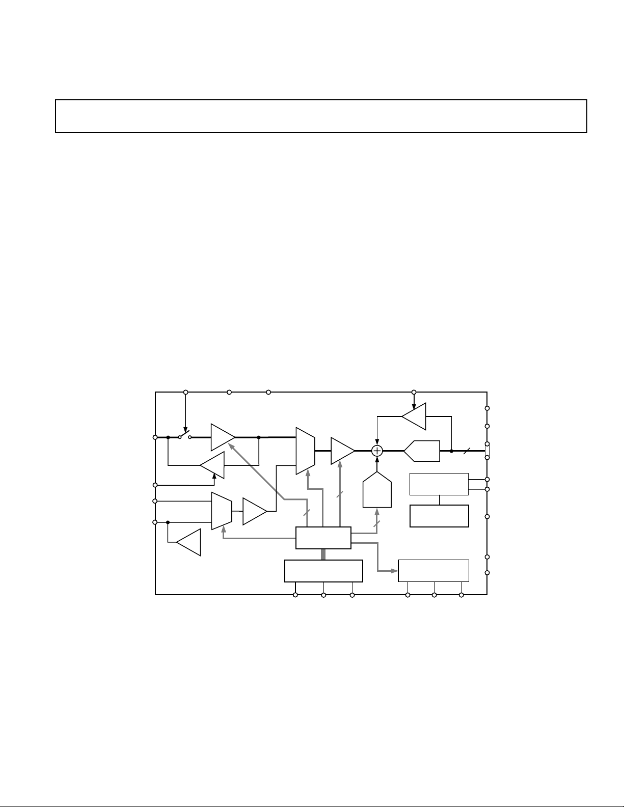
FUNCTIONAL BLOCK DIAGRAM
CCD Signal Processor
AD9840A
PRODUCT DESCRIPTION
The AD9840A is a complete analog signal processor for CCD
applications. It features a 40 MHz single-channel architecture
designed to sample and condition the outputs of interlaced and
progressive scan area CCD arrays. The AD9840A’s signal chain
consists of an input clamp, correlated double sampler (CDS),
digitally controlled variable gain amplifier (VGA), black level
clamp, and 10-bit A/D converter. Additional input modes are
provided for processing analog video signals.
The internal registers are programmed through a 3-wire serial
digital interface. Programmable features include gain adjustment,
black level adjustment, input configuration, and power-down modes.
The AD9840A operates from a 3 V power supply, typically
dissipates 155 mW, and is packaged in a 48-lead LQFP.
CCDIN
CLPDM
AUX1IN
AUX2IN
PBLK
CLP
AVDD
4dB6dB
CDS
CLP
2:1
MUX
AD9840A
BUF
AVSS
2:1
MUX
SL
2dB TO 36dB
VGA
6
INTERNAL
REGISTERS
DIGITAL
INTERFACE
CLPOB
CLP
10-BIT
ADC
BANDGAP
OFFSET
10
DAC
8
SDATASCK
REFERENCE
INTERNAL
BIAS
INTERNAL
TIMING
DATACLKSHDSHP
DRVDD
DRVSS
10
DOUT
VRT
VRB
CML
DVDD
DVSS
REV. 0
Information furnished by Analog Devices is believed to be accurate and
reliable. However, no responsibility is assumed by Analog Devices for its
use, nor for any infringements of patents or other rights of third parties
which may result from its use. No license is granted by implication or
otherwise under any patent or patent rights of Analog Devices.
One Technology Way, P.O. Box 9106, Norwood, MA 02062-9106, U.S.A.
Tel: 781/329-4700 World Wide Web Site: http://www.analog.com
Fax: 781/326-8703 © Analog Devices, Inc., 2000

AD9840A–SPECIFICATIONS
(T
to T
GENERAL SPECIFICATIONS
MIN
, AVDD = DVDD = 3.0 V, f
MAX
Parameter Min Typ Max Unit
TEMPERATURE RANGE
Operating –20 +85 °C
Storage –65 +150 °C
POWER SUPPLY VOLTAGE
Analog, Digital, Digital Driver 2.7 3.6 V
POWER CONSUMPTION
Normal Operation (Specified Under Each Mode of Operation)
Power-Down Modes
Fast Recovery Mode 90 mW
Standby 5 mW
Total Power-Down 1 mW
MAXIMUM CLOCK RATE 40 MHz
A/D CONVERTER
Resolution 10 Bits
Differential Nonlinearity (DNL) ± 0.5 ± 1.0 LSB
No Missing Codes 10 Bits Guaranteed
Full-Scale Input Voltage 2.0 V
Data Output Coding Straight Binary
VOLTAGE REFERENCE
Reference Top Voltage (VRT) 2.0 V
Reference Bottom Voltage (VRB) 1.0 V
Specifications subject to change without notice.
= 40 MHz, unless otherwise noted.)
DATACLK
DIGITAL SPECIFICATIONS
(DRVDD = 2.7 V, CL = 20 pF unless otherwise noted.)
Parameter Symbol Min Typ Max Unit
LOGIC INPUTS
High Level Input Voltage V
Low Level Input Voltage V
High Level Input Current I
Low Level Input Current I
Input Capacitance C
IH
IL
IH
IL
IN
2.1 V
0.6 V
10 µA
10 µA
10 pF
LOGIC OUTPUTS
High Level Output Voltage, IOH = 2 mA V
Low Level Output Voltage, IOL = 2 mA V
Specifications subject to change without notice.
OH
OL
2.2 V
0.5 V
–2–
REV. 0

AD9840A
(T
to T
CCD-MODE SPECIFICATIONS
MIN
, AVDD = DVDD = 3.0 V, f
MAX
Parameter Min Typ Max Unit Notes
P
OWER CONSUMPTION 155 mW
MAXIMUM CLOCK RATE 20 MHz
CDS
Allowable CCD Reset Transient
Max CCD Black Pixel Amplitude
Max Input Range before Saturation
1
1
1
1.0 V p-p With 4 dB CDS Gain
500 mV See Input Waveform in Note 1
200 mV
Max Input Range before Saturation 1.5 V p-p With –2 dB CDS Gain
Max Input Range before Saturation 0.5 V p-p With 10 dB CDS Gain
Max Output Range 1.6 V p-p At Any CDS Gain Setting
Gain Resolution 64 Steps
Gain Range (Two’s Complement Coding) See Figure 15 for CDS Gain Curve
Min Gain (CDS Gain Register Code 32) –2 dB
Medium Gain (CDS Gain Code 63) 4 dB 4 dB is Default with CDS Gain Disabled
Max Gain (CDS Gain Code 31) 10 dB
VARIABLE GAIN AMPLIFIER (VGA)
Max Input Range 1.6 V p-p
Max Output Range 2.0 V p-p
Gain Control Resolution 1024 Steps
Gain Monotonicity Guaranteed
Gain Range See Figure 13 for VGA
Low Gain (VGA Register Code 91) 2 dB See Page 12 for Gain Equations
Max Gain (VGA Code 1023) 36 dB
BLACK LEVEL CLAMP
Clamp Level Resolution 256 Steps
Clamp Level Measured at ADC Output
Min Clamp Level 0 LSB
Max Clamp Level 63.75 LSB
SYSTEM PERFORMANCE Specifications Include Entire Signal Chain
Gain Accuracy, VGA Code 91 to 1023 –1.0 +1.0 dB Use Equations on Page 12 to Calculate Gain
Peak Nonlinearity, 500 mV Input Signal 0.4 % 12 dB Gain Applied (4 dB CDS Gain)
Total Output Noise 0.25 LSB rms AC Grounded Input, 6 dB Gain Applied
Power Supply Rejection (PSR) 40 dB Measured with Step Change on Supply
POWER-UP RECOVERY TIME Clocks Must Be Applied, as in Figures 8 and 9
From Fast Recovery Mode 0.1 ms
From Reference Standby Mode 1 ms
From Total Shutdown Mode 3 ms
From Power-Off Condition 15 ms
NOTES
1
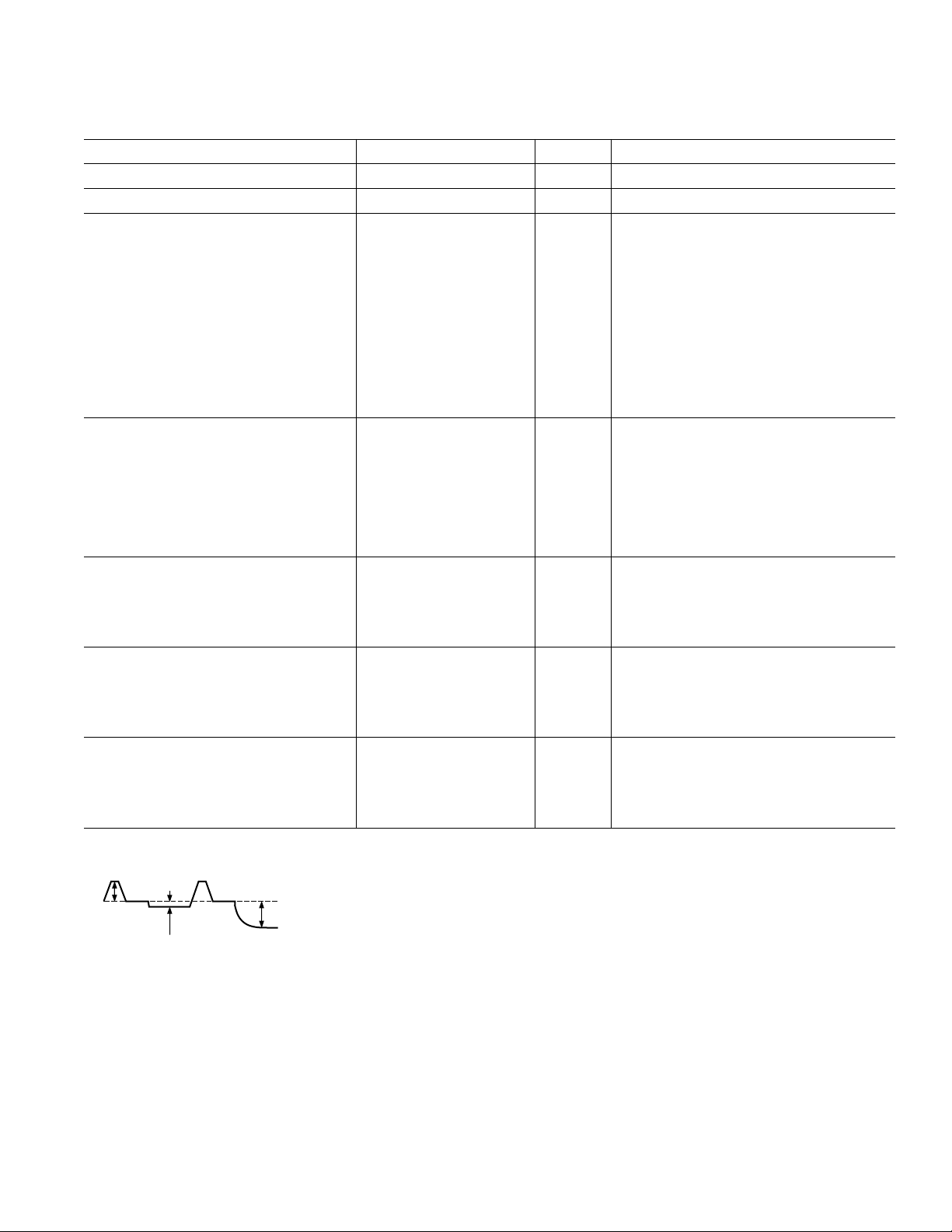
Input Signal Characteristics defined as follows, with 4 dB CDS gain:
DATACLK
= f
SHP
= f
= 40 MHz, unless otherwise noted.)
SHD
Gain Curve
500mV TYP
RESET
TRANSIENT
Specifications subject to change without notice.
200mV MAX
OPTICAL
BLACK PIXEL
1V MAX
INPUT
SIGNAL RANGE
REV. 0
–3–

AD9840A–SPECIFICATIONS
(T
to T
AUX1-MODE SPECIFICATIONS
Parameter Min Typ Max Unit
POWER CONSUMPTION 105 mW
MAXIMUM CLOCK RATE 40 MHz
INPUT BUFFER
Gain 0dB
Max Input Range 1.0 V p-p
VGA
Max Output Range 2.0 V p-p
Gain Control Resolution 1023 Steps
Gain (Selected Using VGA Gain Register)
Min Gain 0 dB
Max Gain 36 dB
Specifications subject to change without notice.
AUX2-MODE SPECIFICATIONS
Parameter Min Typ Max Unit
POWER CONSUMPTION 105 mW
MAXIMUM CLOCK RATE 40 MHz
INPUT BUFFER (Same as AUX1-MODE)
VGA
Max Output Range 2.0 V p-p
Gain Control Resolution 512 Steps
Gain (Selected Using VGA Gain Register)
Min Gain 0 dB
Max Gain 18 dB
ACTIVE CLAMP
Clamp Level Resolution 256 Steps
Clamp Level (Measured at ADC Output)
Min Clamp Level 0 LSB
Max Clamp Level 63.75 LSB
Specification subject to change without notice.
MIN
(T
MIN
, AVDD = DVDD = 3.0 V, f
MAX
to T
, AVDD = DVDD = 3.0 V, f
MAX
= 40 MHz, unless otherwise noted.)
DATACLK
= 40 MHz, unless otherwise noted.)
DATACLK
–4–
REV. 0

AD9840A
TIMING SPECIFICATIONS
(CL = 20 pF, f
Serial Timing in Figures 8–10.)
= 40 MHz, CCD-Mode Timing in Figures 5 and 6, AUX-Mode Timing in Figure 7.
SAMP
Parameter Symbol Min Typ Max Unit
SAMPLE CLOCKS
DATACLK, SHP, SHD Clock Period t
DATACLK Hi/Low Pulsewidth t
SHP Pulsewidth t
SHD Pulsewidth t
CLPDM Pulsewidth t
CLPOB Pulsewidth
1
SHP Rising Edge to SHD Falling Edge t
SHP Rising Edge to SHD Rising Edge t
Internal Clock Delay t
Inhibited Clock Period t
CP
ADC
SHP
SHD
CDM
t
COB
S1
S2
ID
INH
25 ns
10 12.5 ns
56 ns
56 ns
4 10 Pixels
2 20 Pixels
06 ns
10 12.5 ns
3.0 ns
10 ns
DATA OUTPUTS
Output Delay t
Output Hold Time t
OD
H
7.0 7.6 ns
14.5 16 ns
Pipeline Delay 9 Cycles
SERIAL INTERFACE
Maximum SCK Frequency f
SL to SCK Setup Time t
SCK to SL Hold Time t
SDATA Valid to SCK Rising Edge Setup t
SCK Falling Edge to SDATA Valid Hold t
SCK Falling Edge to SDATA Valid Read t
NOTES
1
Minimum CLPOB pulsewidth is for functional operation only. Wider typical pulses are recommended to achieve low noise clamp performance.
Specifications subject to change without notice.
SCLK
LS
LH
DS
DH
DV
10 MHz
10 ns
10 ns
10 ns
10 ns
10 ns
ABSOLUTE MAXIMUM RATINGS
With
Respect
Parameter To Min Max Unit
Model Range Description Option
AD9840AJST –20°C to +85°C Thin Plastic ST-48
ORDERING GUIDE
Temperature Package Package
AVDD1, AVDD2 AVSS –0.3 +3.9 V
DVDD1, DVDD2 DVSS –0.3 +3.9 V
DRVDD DRVSS –0.3 +3.9 V
Digital Outputs DRVSS –0.3 DRVDD + 0.3 V
SHP, SHD, DATACLK DVSS –0.3 DVDD + 0.3 V
CLPOB, CLPDM, PBLK DVSS –0.3 DVDD + 0.3 V
SCK, SL, SDATA DVSS –0.3 DVDD + 0.3 V
VRT, VRB, CMLEVEL AVSS –0.3 AVDD + 0.3 V
THERMAL CHARACTERISTICS
Thermal Resistance
48-Lead LQFP Package
θ
= 92°C
JA
BYP1-4, CCDIN AVSS –0.3 AVDD + 0.3 V
Junction Temperature 150 °C
Lead Temperature 300 °C
(10 sec)
CAUTION
ESD (electrostatic discharge) sensitive device. Electrostatic charges as high as 4000 V readily
accumulate on the human body and test equipment and can discharge without detection. Although
the AD9840A features proprietary ESD protection circuitry, permanent damage may occur on
devices subjected to high-energy electrostatic discharges. Therefore, proper ESD precautions are
recommended to avoid performance degradation or loss of functionality.
Quad Flatpack
(LQFP)
WARNING!
ESD SENSITIVE DEVICE
REV. 0
–5–
 Loading...