Low Power, 8.5 mW, 2.3 V to 5.5 V,
FEATURES
Digitally programmable frequency and phase
8.5 mW power consumption at 2.3 V
MCLK speed: 16 MHz (B grade), 5 MHz (A grade)
28-bit resolution: 0.06 Hz at 16 MHz reference clock
Sinusoidal, triangular, and square wave outputs
2.3 V to 5.5 V power supply
3-wire SPI interface
Extended temperature range: −40°C to +125°C
Power-down option
10-lead LFCSP
APPLICATIONS
Frequency stimulus/waveform generation
Liquid and gas flow measurement
Sensory applications: proximity, motion,
and defect detection
Line loss/attenuation
Test and medical equipment
Sweep/clock generators
Time domain reflectometry (TDR) applications
Programmable Waveform Generator
AD9837
GENERAL DESCRIPTION
The AD9837 is a low power, programmable waveform generator
capable of producing sine, triangular, and square wave outputs.
Waveform generation is required in various types of sensing,
actuation, and time domain reflectometry (TDR) applications.
The output frequency and phase are software programmable,
allowing easy tuning. The frequency registers are 28 bits wide:
with a 16 MHz clock rate, resolution of 0.06 Hz can be achieved;
with a 5 MHz clock rate, the AD9837 can be tuned to 0.02 Hz
resolution.
The AD9837 is written to via a 3-wire serial interface. This serial
interface operates at clock rates up to 40 MHz and is compatible
with DSP and microcontroller standards. The device operates
with a power supply from 2.3 V to 5.5 V.
The AD9837 has a power-down (sleep) function. Sections of the
device that are not being used can be powered down to minimize
the current consumption of the part. For example, the DAC can
be powered down when a clock output is being generated.
The AD9837 is available in a 10-lead LFCSP_WD package.
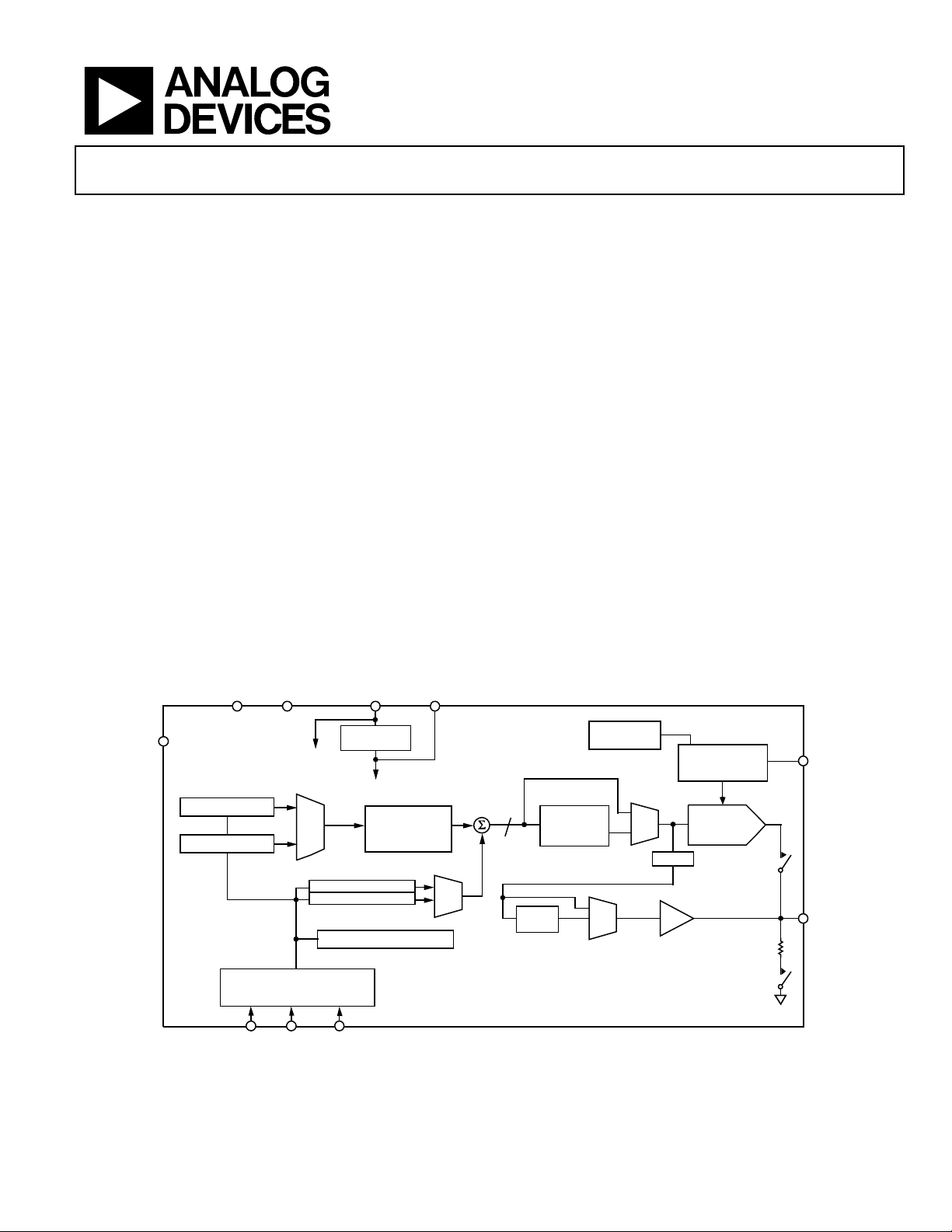
FUNCTIONAL BLOCK DIAGRAM
AGND
MCLK
28-BIT FREQ0 REG
28-BIT FREQ1 REG
Rev. 0
Informatio
n furnished by Analog Devices is believed to be accurate and reliable. However, no
responsibi
lity is assumed by Analog Devices for its use, nor for any infringements of patents or other
rights of th
ird parties that may result from its use. Specifications subject to change without notice. No
license is g
ranted by implication or otherwise under any patent or patent rights of Analog Devices.
Trademar
ks and registered trademarks are the property of their respective owners.
DGND
AVD D/
DVDD
MUX
12-BIT PHASE0 RE G
12-BIT PHASE1 REG
16-BIT CONTROL REGISTER
SERIAL INTERFACE
AND
CONTROL LO GIC
SCLK SDATAFSYNC
VDD
REGULATOR
ACCUMULATOR
2.5V
PHASE
(28-BIT)
CAP/2.5V
MUX
ON-BOARD
REFERENCE
FULL-SCAL E
CONTROL
12
Figure 1.
One Technology Way, P.O. Box 9106, Norwood, MA 02062-9106,
Tel: 781.329.4700 www.analog
Fax: 781.461.3113 ©2011 Analog Devices, Inc. All rights re
DIVIDE
BY 2
SIN
ROM
MUX
AD9837
MUX
10-BIT DAC
MSB
200Ω
COMP
VOUT
R
9070-001
U.S.A.
.com
served.

AD9837
TABLE OF CONTENTS
Features .............................................................................................. 1
Applications ....................................................................................... 1
General Description ......................................................................... 1
Functional Block Diagram .............................................................. 1
Revision History ............................................................................... 2
Specifications ..................................................................................... 3
Timing Characteristics ................................................................ 4
Absolute Maximum Ratings ............................................................ 5
Thermal Resistance ...................................................................... 5
ESD Caution .................................................................................. 5
Pin Configuration and Function Descriptions ............................. 6
Typical Performance Characteristics ............................................. 7
Test Circuit ........................................................................................ 9
Terminology .................................................................................... 10
Theory of Operation ...................................................................... 11
Circuit Description ......................................................................... 12
Numerically Controlled Oscillator Plus Phase Modulator ... 12
SIN ROM ..................................................................................... 12
Digital-to-Analog Converter (DAC) ....................................... 12
Regulator ...................................................................................... 12
REVISION HISTORY
4/11—Revision 0: Initial Version
Functional Description .................................................................. 13
Serial Interface ............................................................................ 13
Latency Period ............................................................................ 13
Control Register ......................................................................... 13
Frequency and Phase Registers ................................................ 15
Reset Function ............................................................................ 16
Sleep Function ............................................................................ 16
VOUT Pin ................................................................................... 16
Powering Up the AD9837 ......................................................... 16
Applications Information .............................................................. 19
Grounding and Layout .............................................................. 19
Interfacing to Microprocessors................................................. 19
Evaluation Board ............................................................................ 21
System Demonstration Platform .............................................. 21
AD9837 to SPORT Interface ..................................................... 21
Evaluation Kit ............................................................................. 21
Crystal Oscillator vs. External Clock ....................................... 21
Power Supply ............................................................................... 21
Evaluation Board Schematics ................................................... 22
Evaluation Board Layout ........................................................... 24
Outline Dimensions ....................................................................... 25
Ordering Guide .......................................................................... 25
Rev. 0 | Page 2 of 28

AD9837
SPECIFICATIONS
VDD = 2.3 V to 5.5 V, AGND = DGND = 0 V, TA = T
Table 1.
1
Parameter
Min Typ Max Unit Test Conditions/Comments
SIGNAL DAC SPECIFICATIONS
Resolution 10 Bits
Update Rate
A Grade 5 MSPS
B Grade 16 MSPS
V
Maximum 0.645 V
OUT
V
Minimum 37 mV
OUT
V
0.610 V
p-p
V
TC 200 ppm/°C
OUT
DC Accuracy
Integral Nonlinearity (INL) ±1.0 LSB
Differential Nonlinearity (DNL) ±0.5 LSB
DDS SPECIFICATIONS
Dynamic Specifications
Signal-to-Noise Ratio (SNR)
A Grade −64 dB f
B Grade −64 dB f
Total Harmonic Distortion (THD)
A Grade −68 dBc f
B Grade −68 dBc f
Spurious-Free Dynamic Range (SFDR)
Wideband (0 to Nyquist)
A Grade −65 dBc f
B Grade −65 dBc f
Narrow-Band (±200 kHz)
A Grade −94 dBc f
B Grade −97 dBc f
Clock Feedthrough −67 dBc
Wake-Up Time 1 ms
LOGIC INPUTS
Input High Voltage, V
1.7 V 2.3 V to 2.7 V power supply
INH
2.0 V 2.7 V to 3.6 V power supply
2.8 V 4.5 V to 5.5 V power supply
Input Low Voltage, V
0.5 V 2.3 V to 2.7 V power supply
INL
0.7 V 2.7 V to 3.6 V power supply
0.8 V 4.5 V to 5.5 V power supply
Input Current, I
10 mA
INH/IINL
Input Capacitance, CIN 3 pF
POWER SUPPLIES f
VDD 2.3 5.5 V
IDD
A Grade 3.7 5.0 mA IDD code dependent; see Figure 6
B Grade 4.5 5.5 mA IDD code dependent; see Figure 7
Low Power Sleep Mode 0.5 0.8 mA
1
Operating temperature range is −40°C to +125°C; typical specifications are at 25°C.
MIN
to T
, unless otherwise noted.
MAX
= 5 MHz, f
MCLK
= 16 MHz, f
MCLK
= 5 MHz, f
MCLK
= 16 MHz, f
MCLK
= 5 MHz, f
MCLK
= 16 MHz, f
MCLK
= 5 MHz, f
MCLK
= 16 MHz, f
MCLK
= 16 MHz, f
MCLK
OUT
OUT
OUT
OUT
OUT
OUT
OUT
OUT
OUT
= f
= f
= f
= f
= f
= f
= f
= f
= f
MCLK
MCLK
MCLK
MCLK
MCLK
MCLK
MCLK
MCLK
MCLK
/4096
/4096
/4096
/4096
/50
/50
/50
/50
/4096
DAC powered down (SLEEP1 and
SLEEP12 bits = 11; see Table 15)
Rev. 0 | Page 3 of 28
AD9837
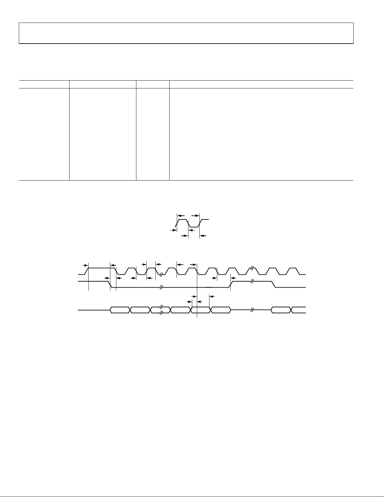
TIMING CHARACTERISTICS
VDD = 2.3 V to 5.5 V, AGND = DGND = 0 V, unless otherwise noted.
Table 2.
1
Parameter
t1 62.5 ns min MCLK period (f
t2 25 ns min MCLK high duration (f
t3 25 ns min MCLK low duration (f
Limit at T
MIN
to T
Unit Description
MAX
= 16 MHz)
MCLK
= 16 MHz)
MCLK
= 16 MHz)
MCLK
t4 25 ns min SCLK period
t5 10 ns min SCLK high duration
t6 10 ns min SCLK low duration
t7 5 ns min FSYNC to SCLK falling edge setup time
t8 10 ns min SCLK falling edge to FSYNC rising edge time
t
− 5 ns max
4
t9 5 ns min Data setup time
t10 3 ns min Data hold time
t11 5 ns min SCLK high to FSYNC falling edge setup time
1
Guaranteed by design; not production tested.
Timing Diagrams
t
1
MCLK
t
2
t
3
9070-003
Figure 2. Master Clock
SCLK
FSYNC
t
11
t
7
t
5
t
6
t
4
t
8
t
10
t
9
SDATA
D15
41D51DD0D1D2D14
09070-004
Figure 3. Serial Timing
Rev. 0 | Page 4 of 28
AD9837
ABSOLUTE MAXIMUM RATINGS
TA = 25°C, unless otherwise noted.
Table 3.
Parameter Rating
VDD to AGND −0.3 V to +6 V
VDD to DGND −0.3 V to +6 V
AGND to DGND −0.3 V to +0.3 V
CAP/2.5V 2.75 V
Digital I/O Voltage to DGND −0.3 V to VDD + 0.3 V
Analog I/O Voltage to AGND −0.3 V to VDD + 0.3 V
Operating Temperature Range
Industrial (B Version) −40°C to +125°C
Storage Temperature Range −65°C to +150°C
Maximum Junction Temperature 150°C
Lead Temperature, Soldering (10 sec) 300°C
IR Reflow, Peak Temperature 220°C
Stresses above those listed under Absolute Maximum Ratings
may cause permanent damage to the device. This is a stress
rating only; functional operation of the device at these or any
other conditions above those indicated in the operational
section of this specification is not implied. Exposure to absolute
maximum rating conditions for extended periods may affect
device reliability.
THERMAL RESISTANCE
θJA is specified for the worst-case conditions, that is, a device
soldered in a circuit board for surface-mount packages.
Table 4. Thermal Resistance
Package Type θJA θ
10-Lead LFCSP_WD (CP-10-9) 206 44 °C/W
Unit
JC
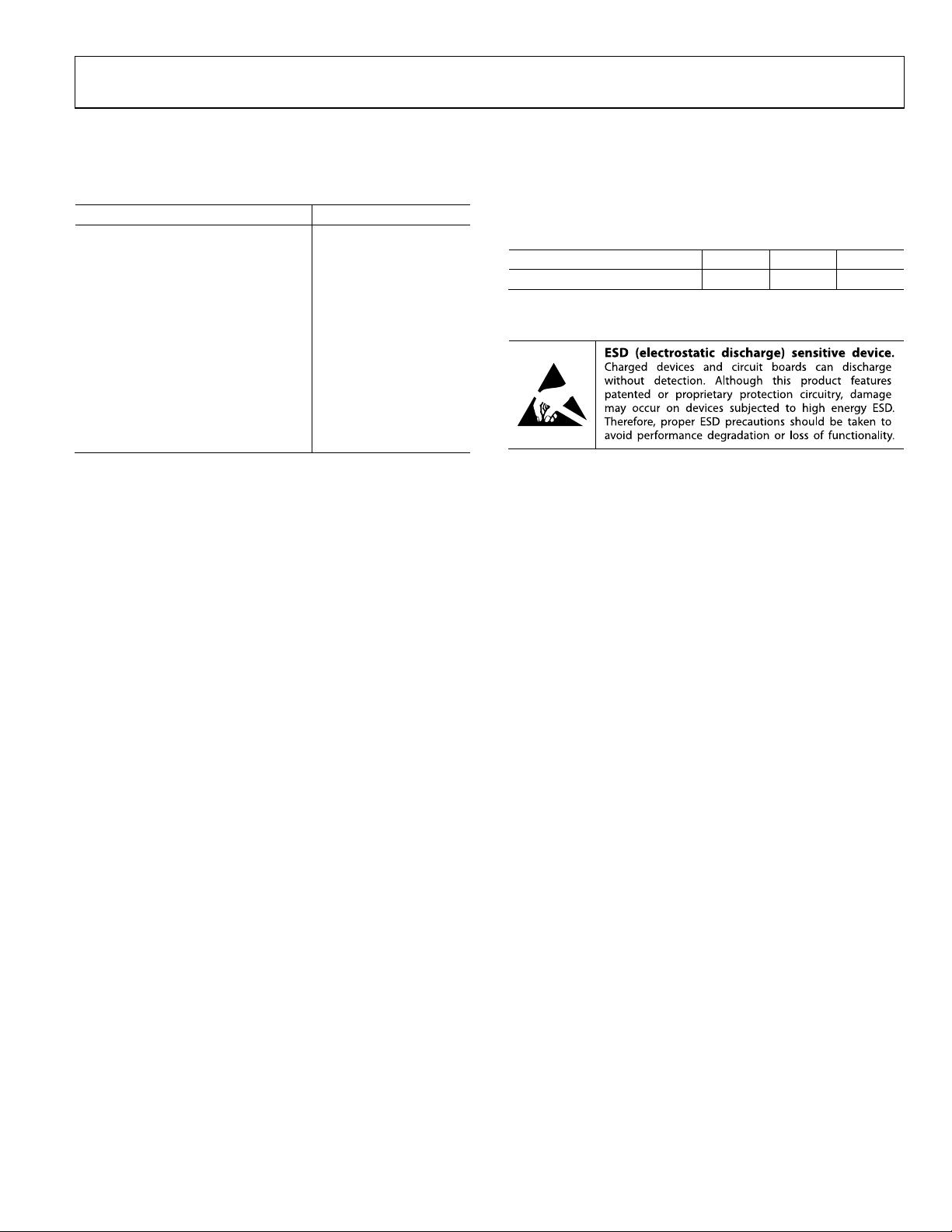
ESD CAUTION
Rev. 0 | Page 5 of 28

AD9837
PIN CONFIGURATION AND FUNCTION DESCRIPTIONS
1
COMP
VDD
2
CAP/2.5V
DGND
MCLK
NOTES
1. CONNECT EXP OSED PAD
TO GROUND.
AD9837
3
TOP VIEW
(Not to Scale)
4
5
Figure 4. Pin Configuration
Table 5. Pin Function Descriptions
Pin No. Mnemonic Description
1 COMP DAC Bias Pin. This pin is used for decoupling the DAC bias voltage.
2 VDD
Positive Power Supply for the Analog and Digital Interface Sections. The on-board 2.5 V regulator is also
supplied from VDD. VDD can have a value from 2.3 V to 5.5 V. A 0.1 μF and a 10 μF decoupling capacitor should
be connected between VDD and AGND.
3 CAP/2.5V
The digital circuitry operates from a 2.5 V power supply. This 2.5 V is generated from VDD using an on-board
regulator when VDD exceeds 2.7 V. The regulator requires a decoupling capacitor of 100 nF typical, which is
connected from CAP/2.5V to DGND. If VDD is less than or equal to 2.7 V, CAP/2.5V should be tied directly to
VDD to bypass the on-board regulator.
4 DGND Digital Ground.
5 MCLK
Digital Clock Input. DDS output frequencies are expressed as a binary fraction of the frequency of MCLK. The
output frequency accuracy and phase noise are determined by this clock.
6 SDATA Serial Data Input. The 16-bit serial data-word is applied to this input.
7 SCLK Serial Clock Input. Data is clocked into the AD9837 on each falling edge of SCLK.
8 FSYNC
Active Low Control Input. FSYNC is the frame synchronization signal for the input data. When FSYNC is taken
low, the internal logic is informed that a new word is being loaded into the device.
9 AGND Analog Ground.
10 VOUT
Voltage Output. The analog and digital output from the AD9837 is available at this pin. An external load
resistor is not required because the device has a 200 Ω resistor on board.
EP Exposed Pad. Connect the exposed pad to ground.
10
9
8
7
6
VOUT
AGND
FSYNC
SCLK
SDATA
09070-005
Rev. 0 | Page 6 of 28
AD9837
–
–
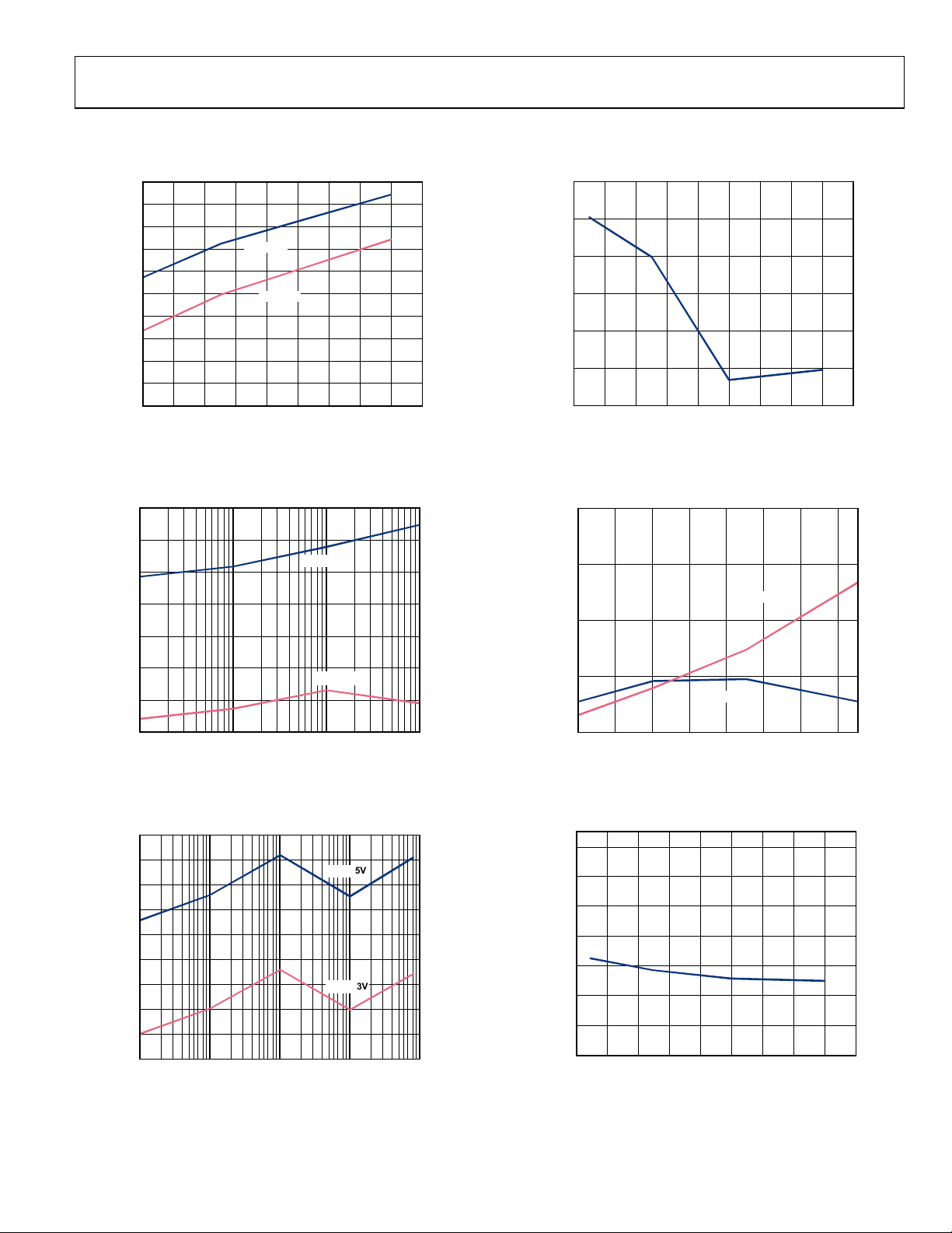
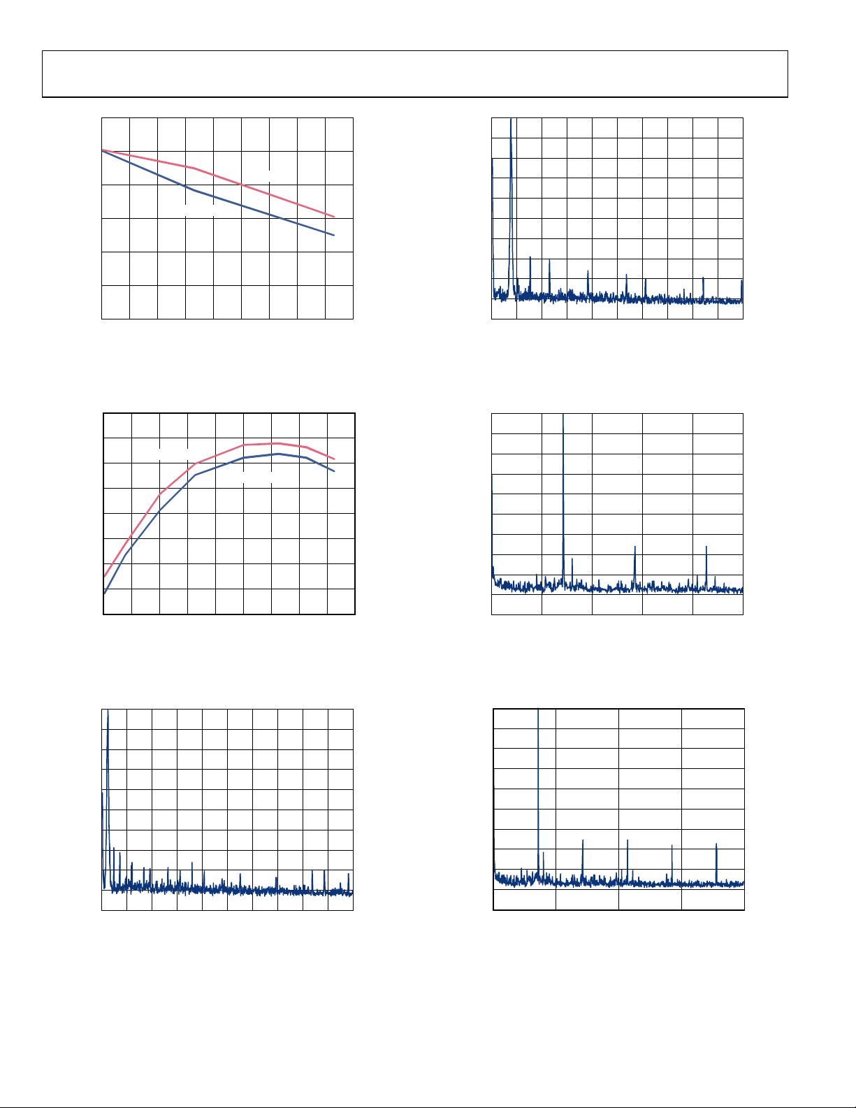
TYPICAL PERFORMANCE CHARACTERISTICS
5.0
4.8
4.6
4.4
4.2
4.0
(mA)
DD
I
3.8
3.6
3.4
3.2
3.0
0 2 4 6 8 1012141618
VDD = 5V
VDD = 3V
MCLK FREQUENCY ( MHz)
Figure 5. Typical Current Consumption (IDD) vs. MCLK Frequency
= MCLK/10
for f
OUT
6
09070-00
98
–99
–100
–101
SFDR (dB)
–102
–103
–104
02468 1816141210
MCLK FREQUENCY ( MHz)
Figure 8. Narrow-Band SFDR vs. MCLK Frequency,
= MCLK/50 to ±200 kHz
f
OUT
09070-009
4.5
4.4
4.3
4.2
(mA)
DD
4.1
I
4.0
3.9
3.8
1 10 100 1000
OUTPUT FREQUENCY (kHz)
Figure 6. Typical IDD vs. Output Frequency for f
4.9
4.8
4.7
4.6
4.5
(mA)
4.4
DD
I
4.3
4.2
4.1
4.0
1 10 100 1k 10k
OUTPUT FREQUENCY (kHz)
Figure 7. Typical IDD vs. Output Frequency for f
VDD = 5V
VDD = 3V
MCLK
VDD = 5V
VDD = 3V
MCLK
= 5 MHz
= 16 MHz
50
–55
MCLK/7
–60
SFDR (dB)
–65
MCLK/50
–70
1 3 5 7 9 11 13 15
09070-007
MCLK FREQUENCY (MHz)
09070-010
Figure 9. Wideband SFDR vs. MCLK Frequency
–56
–58
–60
–62
SNR (dB)
–64
–66
–68
–70
0 2 4 6 8 1012141618
09070-008
MCLK FREQUENCY ( MHz)
09070-011
Figure 10. SNR vs. MCLK Frequency
Rev. 0 | Page 7 of 2
8
AD9837
1000
900
800
700
600
WAKE-UP TI ME (µs)
500
400
–40 –20 0 20 40 60 80 140120100
VDD = 5.5V
TEMPERATURE (°C)
Figure 11. Wake-Up Time vs. Temperature
VDD = 2.3V
09070-012
0
–10
–20
–30
–40
–50
–60
POWER (dB)
–70
–80
–90
–100
0 1009010 20 30 40 50 60 70 80
Figure 14. Power vs. Frequency, f
FREQUENCY (kHz)
= 16 MHz, f
MCLK
Frequency Word = 0x1F81A
= 7.692 kHz,
OUT
09070-015
1.180
1.178
1.176
1.174
(V)
1.172
REF
V
1.170
1.168
1.166
1.164
–40 –20 0 20 40 60 80 100 140120
0
–10
–20
–30
–40
–50
–60
POWER (dB)
–70
–80
–90
–100
0 1009010 20 30 40 50 60 70 80
Figure 13. Power vs. Frequency, f
VDD = 2.7V
Figure 12. V
VDD = 5.0V
TEMPERATURE ( °C)
vs. Temperature
REF
FREQUENCY (kHz)
= 5 MHz, f
MCLK
Frequency Word = 0x1F751
= 2.4 kHz,
OUT
0
–10
–20
–30
–40
–50
–60
POWER (dB)
–70
–80
–90
–100
09070-013
02.50.5 1.0 1.5 2.0
Figure 15. Power vs. Frequency, f
FREQUENCY (MHz)
= 5 MHz, f
MCLK
= 0.714285 MHz = f
OUT
MCLK
09070-016
/7,
Frequency Word = 0x2492492
0
–10
–20
–30
–40
–50
–60
POWER (dB)
–70
–80
–90
–100
04123
09070-014
Figure 16. Power vs. Frequency, f
FREQUENCY (MHz)
= 16 MHz, f
MCLK
= 2.285714 MHz = f
OUT
MCLK
7
09070-01
/7,
Frequency Word = 0x2492492
Rev. 0 | Page 8 of 2
8

AD9837
TEST CIRCUIT
100nF
CAP/2.5V
REGULATOR
COMP
12
SIN
ROM
10-BIT DAC
10nF
VDD
VOUT
20pF
AD9837
09070-002
Figure 17. Test Circuit Used to Test Specifications
Rev. 0 | Page 9 of 28
 Loading...