REV. 0
Information furnished by Analog Devices is believed to be accurate and
reliable. However, no responsibility is assumed by Analog Devices for its
use, nor for any infringements of patents or other rights of third parties
which may result from its use. No license is granted by implication or
otherwise under any patent or patent rights of Analog Devices.
a
AD9835
One Technology Way, P.O. Box 9106, Norwood, MA 02062-9106, U.S.A.
Tel: 781/329-4700 World Wide Web Site: http://www.analog.com
Fax: 781/326-8703 © Analog Devices, Inc., 1998
50 MHz CMOS
Complete DDS
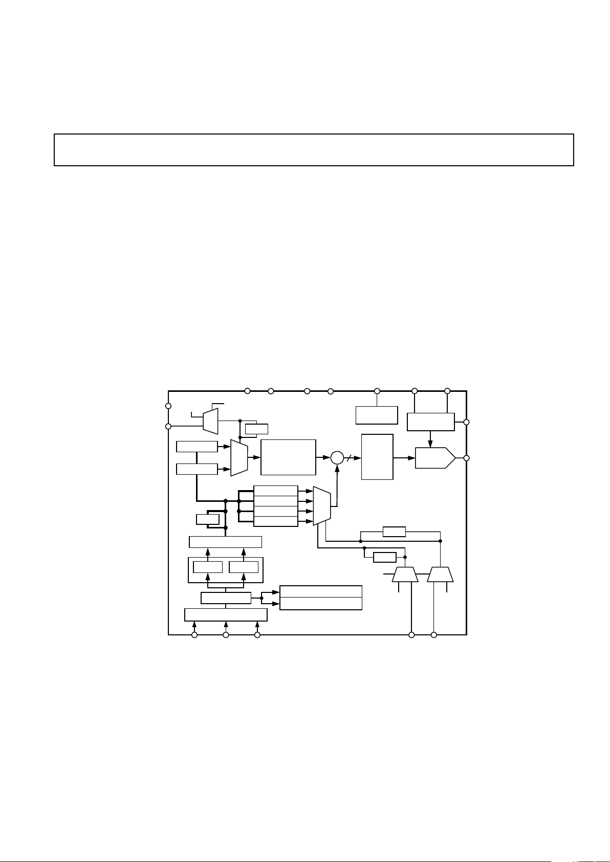
FUNCTIONAL BLOCK DIAGRAM
IOUT
COMP
REFINFS ADJUST
REFOUT
AGND
AVDDDGND
DVDD
MCLK
PSEL0
PSEL1
12
Σ
AD9835
ON-BOARD
REFERENCE
10-BIT
DAC
PHASE0 REG
PHASE1 REG
PHASE2 REG
PHASE3 REG
FULL-SCALE
CONTROL
COS
ROM
PHASE
ACCUMULATOR
(32 BIT)
MUX
FREQ0 REG
FREQ1 REG
MUX
16-BIT DATA REGISTER
SYNC
FSELECT
FSELECT
BIT
SELSRC
SYNC
8 LSBs8 MSBs
DECODE LOGIC
FSYNC SCLK SDATA
SERIAL REGISTER
CONTROL REGISTER
FSELECT/PSEL REGISTER
DEFER REGISTER
SYNC
SYNC
SELSRC
PSEL0
BIT
PSEL1
BIT
FEATURES
5 V Power Supply
50 MHz Speed
On-Chip COS Look-Up Table
On-Chip 10-Bit DAC
Serial Loading
Power-Down Option
200 mW Power Consumption
16-Lead TSSOP
APPLICATIONS
DDS Tuning
Digital Demodulation
GENERAL DESCRIPTION
The AD9835 is a numerically controlled oscillator employing
a phase accumulator, a COS Look-Up Table and a 10-bit
D/A converter integrated on a single CMOS chip. Modulation
capabilities are provided for phase modulation and frequency
modulation.
Clock rates up to 50 MHz are supported. Frequency accuracy
can be controlled to one part in 4 billion. Modulation is effected by loading registers through the serial interface. A
power-down bit allows the user to power down the AD9835 when
it is not in use, the power consumption being reduced to 1.75 mW.
The part is available in a 16-lead TSSOP package.

–2– REV. 0
AD9835–SPECIFICATIONS
1
(VDD = +5 V ⴞ 5%; AGND = DGND = 0 V; TA = T
MIN
to T
MAX
; REFIN = REFOUT;
R
SET
= 3.9 k⍀; R
LOAD
= 300 ⍀ for IOUT, unless otherwise noted)
Parameter AD9835B Units Test Conditions/Comments
SIGNAL DAC SPECIFICATIONS
Resolution 10 Bits
Update Rate (f
MAX
) 50 MSPS nom
IOUT Full Scale 4 mA
nom
4.75 mA max
Output Compliance 1.35 V max
DC Accuracy
Integral Nonlinearity ±1 LSB typ
Differential Nonlinearity ±0.5 LSB typ
DDS SPECIFICATIONS
2
Dynamic Specifications
Signal-to-Noise Ratio 50 dB min f
MCLK
= 50 MHz, f
OUT
= 1 MHz
Total Harmonic Distortion –52 dBc max f
MCLK
= 50 MHz, f
OUT
= 1 MHz
Spurious Free Dynamic Range (SFDR)
3
f
MCLK
= 6.25 MHz, f
OUT
= 2.11 MHz
Narrow Band (±50 kHz) –72 dBc min
Wide Band (±2 MHz) –50 dBc min
Clock Feedthrough –60 dBc typ
Wake-Up Time 1 ms typ
Power-Down Option Yes
VOLTAGE REFERENCE
Internal Reference @ +25°C 1.21 V typ
T
MIN
to T
MAX
1.21 ± 7% V min/max
REFIN Input Impedance 10 MΩ typ
Reference TC 100 ppm/°C typ
REFOUT Output Impedance 300 Ω typ
LOGIC INPUTS
V
INH
, Input High Voltage DVDD – 0.9 V min
V
INL
, Input Low Voltage 0.9 V max
I
INH
, Input Current 10 µA
max
CIN, Input Capacitance 10 pF max
POWER SUPPLIES f
MCLK
= 50 MHz
AVDD 4.75/5.25 V
min/V max
DVDD 4.75/5.25 V
min/V max
I
AA
5mA
max
I
DD
2.5 + 0.33/MHz mA typ
I
AA
+ I
DD
4
40 mA max
Low Power Sleep Mode 0.35 mA max
NOTES
1
Operating temperature range is as follows: B Version: –40 °C to +85°C.
2
100% production tested.
3
f
MCLK
= 6.25 MHz, Frequency Word = 5671C71C HEX, f
OUT
= 2.11 MHz.
4
Measured with the digital inputs static and equal to 0 V or DVDD. The AD9835 is tested with a capacitive load of 50 pF. The part can be operated with higher
capacitive loads, but the magnitude of the analog output will be attenuated. See Figure 5.
Specifications subject to change without notice.
IOUT
COMP
REFIN
FS
ADJUST
REFOUT
12
AD9835
ON-BOARD
REFERENCE
10-BIT
DAC
COS
ROM
FULL-SCALE
CONTROL
300V 50pF
R
SET
3.9kV
10nF
10nF
AVDD
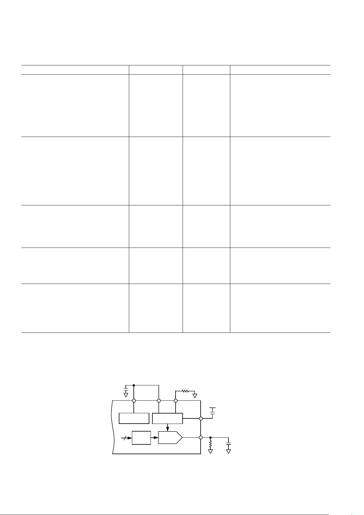
Figure 1. Test Circuit with Which Specifications Are Tested

AD9835
–3–REV. 0
TIMING CHARACTERISTICS
(VDD = +5 V ⴞ 5%; AGND = DGND = 0 V, unless otherwise noted)
Limit at
T
MIN
to T
MAX
Parameter (B Version) Units Test Conditions/Comments
t
1
20 ns min MCLK Period
t
2
8 ns min MCLK High Duration
t
3
8 ns min MCLK Low Duration
t
4
50 ns min SCLK Period
t
5
20 ns min SCLK High Duration
t
6
20 ns min SCLK Low Duration
t
7
15 ns min FSYNC to SCLK Falling Edge Setup Time
t
8
20 ns min FSYNC to SCLK Hold Time
SCLK – 5 ns max
t
9
15 ns min Data Setup Time
t
10
5 ns min Data Hold Time
t
11
8 ns min FSELECT, PSEL0, PSEL1 Setup Time Before MCLK Rising Edge
t
11A
1
8 ns min FSELECT, PSEL0, PSEL1 Setup Time After MCLK Rising Edge
NOTES
1
See Pin Description section.
Guaranteed by design but not production tested.
MCLK
t
2
t
1
t
3
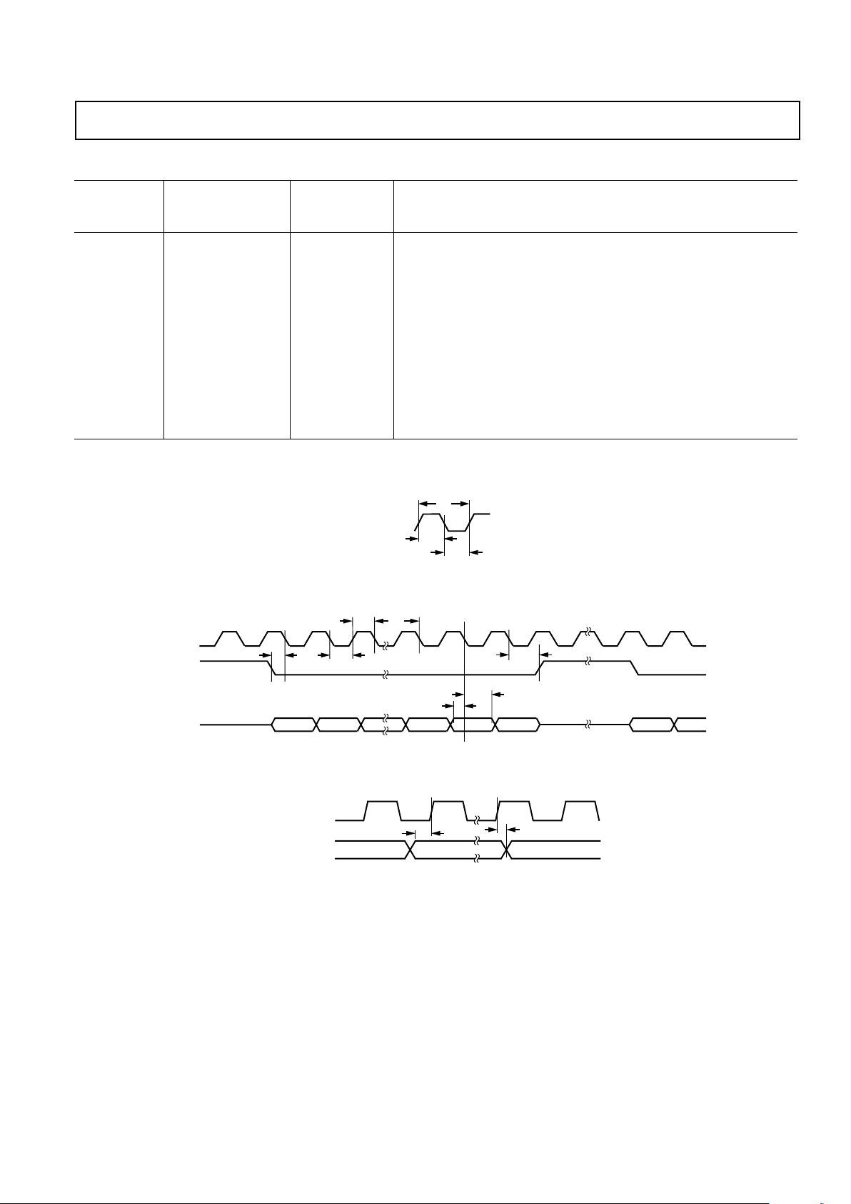
Figure 2. Master Clock
SCLK
FSYNC
SDATA
t
5
t
4
t
6
t
7
t
8
t
10
t
9
D15 D14 D2 D1 D0 D15 D14
Figure 3. Serial Timing
t
11A
t
11
VALID DATA VALID DATA VALID DATA
MCLK
FSELECT
PSEL0, PSEL1
Figure 4. Control Timing

AD9835
–4– REV. 0
ABSOLUTE MAXIMUM RATINGS*
(T
A
= +25°C unless otherwise noted)
AVDD to AGND . . . . . . . . . . . . . . . . . . . . . . –0.3 V to +7 V
DVDD to DGND . . . . . . . . . . . . . . . . . . . . . . –0.3 V to +7 V
AVDD to DVDD . . . . . . . . . . . . . . . . . . . . . –0.3 V to +0.3 V
AGND to DGND. . . . . . . . . . . . . . . . . . . . . .–0.3 V to +0.3 V
Digital I/O Voltage to DGND . . . . . –0.3 V to DVDD + 0.3 V
Analog I/O Voltage to AGND . . . . . –0.3 V to AVDD + 0.3 V
Operating Temperature Range
Industrial (B Version) . . . . . . . . . . . . . . . . –40°C to +85°C
Storage Temperature Range . . . . . . . . . . . . –65°C to +150°C
Maximum Junction Temperature . . . . . . . . . . . . . . . .+150°C
TSSOP θ
JA
Thermal Impedance . . . . . . . . . . . . . . . 158°C/W
Lead Temperature, Soldering
Vapor Phase (60 sec) . . . . . . . . . . . . . . . . . . . . . . . .+215°C
Infrared (15 sec) . . . . . . . . . . . . . . . . . . . . . . . . . . . .+220°C
ESD Rating . . . . . . . . . . . . . . . . . . . . . . . . . . . . . . . > 4500 V
*Stresses above those listed under Absolute Maximum Ratings may cause perma-
nent damage to the device. This is a stress rating only; functional operation of the
device at these or any other conditions above those listed in the operational sections
of this specification is not implied. Exposure to absolute maximum rating conditions for extended periods may affect device reliability.
ORDERING GUIDE
Temperature Package Package
Model Range Description Option*
AD9835BRU –40°C to +85°C 16-Lead TSSOP RU-16
*RU = Thin Shrink Small Outline Package (TSSOP).
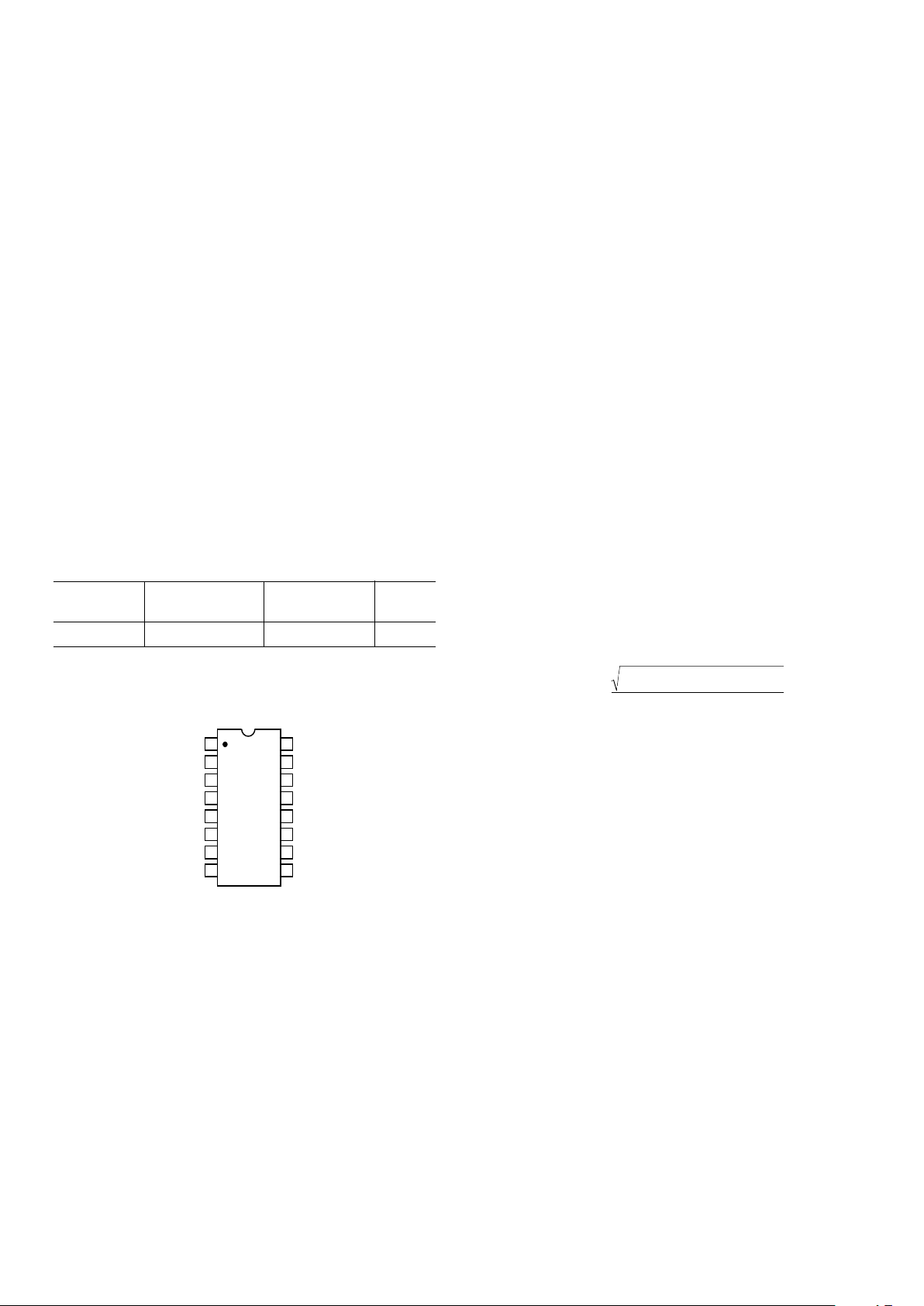
PIN CONFIGURATION
14
13
12
11
16
15
10
9
8
1
2
3
4
7
6
5
TOP VIEW
(Not to Scale)
AD9835
FS ADJUST
AGND
IOUT
AVDD
COMP
REFIN
REFOUT
DVDD
FSELECT
PSEL1
PSEL0
DGND
MCLK
SCLK
SDATA
FSYNC
TERMINOLOGY
Integral Nonlinearity
This is the maximum deviation of any code from a straight line
passing through the endpoints of the transfer function. The endpoints of the transfer function are zero scale, a point 0.5 LSB
below the first code transition (000 . . . 00 to 000 . . . 01)
and full scale, a point 0.5 LSB above the last code transition
(111 . . . 10 to 111 . . . 11). The error is expressed in LSBs.
Differential Nonlinearity
This is the difference between the measured and ideal 1 LSB
change between two adjacent codes in the DAC.
Signal to (Noise + Distortion)
Signal to (Noise + Distortion) is measured signal to noise at the
output of the DAC. The signal is the rms magnitude of the
fundamental. Noise is the rms sum of all the nonfundamental
signals up to half the sampling frequency (f
MCLK
/2) but excluding the dc component. Signal to (Noise + Distortion) is dependent on the number of quantization levels used in the digitization
process; the more levels, the smaller the quantization noise.
The theoretical Signal to (Noise + Distortion) ratio for a sine
wave input is given by
Signal to (Noise + Distortion) = (6.02N + 1.76) dB
where N is the number of bits. Thus, for an ideal 10-bit converter, Signal to (Noise + Distortion) = 61.96 dB.
Total Harmonic Distortion
Total Harmonic Distortion (THD) is the ratio of the rms sum
of harmonics to the rms value of the fundamental. For the
AD9835, THD is defined as
THD = 20 log
(V
2
2
+V
3
2
+V
4
2
+V
5
2
+V
6
2
)
V
1
where V1 is the rms amplitude of the fundamental and V2, V3,
V
4
, V5 and V6 are the rms amplitudes of the second through the
sixth harmonic.
Output Compliance
The output compliance refers to the maximum voltage that can
be generated at the output of the DAC to meet the specifications. When voltages greater than that specified for the output
compliance are generated, the AD9835 may not meet the specifications listed in the data sheet.
Spurious Free Dynamic Range
Along with the frequency of interest, harmonics of the fundamental frequency and images of the MCLK frequency are
present at the output of a DDS device. The spurious free dynamic range (SFDR) refers to the largest spur or harmonic
present in the band of interest. The wideband SFDR gives the
magnitude of the largest harmonic or spur relative to the magni-
tude of the fundamental frequency in the bandwidth ±2 MHz
about the fundamental frequency. The narrow band SFDR gives
the attenuation of the largest spur or harmonic in a bandwidth of
±50 kHz about the fundamental frequency.
Clock Feedthrough
There will be feedthrough from the MCLK input to the analog
output. Clock feedthrough refers to the magnitude of the
MCLK signal relative to the fundamental frequency in the
AD9835’s output spectrum.

AD9835
–5–REV. 0
PIN FUNCTION DESCRIPTIONS
Pin # Mnemonic Function
ANALOG SIGNAL AND REFERENCE
1 FS ADJUST Full-Scale Adjust Control. A resistor (R
SET
) is connected between this pin and AGND. This determines
the magnitude of the full-scale DAC current. The relationship between R
SET
and the full-scale current is
as follows:
IOUT
FULL-SCALE
= 12.5 × V
REFIN/RSET
V
REFIN
= 1.21 V nominal, R
SET
= 3.9 kΩ typical
2 REFIN Voltage Reference Input. The AD9835 can be used with either the onboard reference, which is available
from pin REFOUT, or an external reference. The reference to be used is connected to the REFIN pin.
The AD9835 accepts a reference of 1.21 V nominal.
3 REFOUT Voltage Reference Output. The AD9835 has an onboard reference of value 1.21 V nominal. The refer-
ence is made available on the REFOUT pin. This reference is used as the reference to the DAC by connecting REFOUT to REFIN. REFOUT should be decoupled with a 10 nF capacitor to AGND.
14 IOUT Current Output. This is a high impedance current source. A load resistor should be connected between
IOUT and AGND.
16 COMP Compensation pin. This is a compensation pin for the internal reference amplifier. A 10 nF decoupling
ceramic capacitor should be connected between COMP and AVDD.
POWER SUPPLY
4 DVDD Positive Power Supply for the Digital Section. A 0.1 µF decoupling capacitor should be connected be-
tween DVDD and DGND. DVDD can have a value of +5 V ± 5%.
5 DGND Digital Ground.
13 AGND Analog Ground.
15 AVDD Positive Power Supply for the Analog Section. A 0.1 µF decoupling capacitor should be connected be-
tween AVDD and AGND. AVDD can have a value of +5 V ± 5%.
DIGITAL INTERFACE AND CONTROL
6 MCLK Digital Clock Input. DDS output frequencies are expressed as a binary fraction of the frequency of MCLK.
The output frequency accuracy and phase noise are determined by this clock.
7 SCLK Serial Clock, Logic Input. Data is clocked into the AD9835 on each falling SCLK edge.
8 SDATA Serial Data In, Logic Input. The 16-bit serial data word is applied to this input.
9 FSYNC Data Synchronization Signal, Logic Input. When this input is taken low, the internal logic is informed
that a new word is being loaded into the device.
10 FSELECT Frequency Select Input. FSELECT controls which frequency register, FREQ0 or FREQ1, is used in the
phase accumulator. The frequency register to be used can be selected using the pin FSELECT or the bit
FSELECT. FSELECT is sampled on the rising MCLK edge. FSELECT needs to be in steady state
when an MCLK rising edge occurs. If FSELECT changes value when a rising edge occurs, there is an
uncertainty of one MCLK cycle as to when control is transferred to the other frequency register. To avoid
any uncertainty, a change on FSELECT should not coincide with an MCLK rising edge. When the bit is
being used to select the frequency register, the pin FSELECT should be tied to DGND.
11, 12 PSEL0, PSEL1 Phase Select Input. The AD9835 has four phase registers. These registers can be used to alter the value
being input to the COS ROM. The contents of the phase register are added to the phase accumulator output, the inputs PSEL0 and PSEL1 selecting the phase register to be used. Alternatively, the
phase register to be used can be selected using bits PSEL0 and PSEL1. Like the FSELECT input,
PSEL0 and PSEL1 are sampled on the rising MCLK edge. Therefore, these inputs need to be in
steady state when an MCLK rising edge occurs or there is an uncertainty of one MCLK cycle as to
when control is transferred to the selected phase register. When the phase registers are being controlled by the bits PSEL0 and PSEL1, the pins should be tied to DGND.
 Loading...