ANALOG DEVICES AD9834 Service Manual
20 mW Power, 2.3 V to 5.5 V,
FEATURES
Narrow-band SFDR >72 dB
2.3 V to 5.5 V power supply
Output frequency up to 37.5 MHz
Sine output/triangular output
On-board comparator
3-wire SPI® interface
Extended temperature range: −40°C to +105°C
Power-down option
20 mW power consumption at 3 V
20-lead TSSOP
APPLICATIONS
Frequency stimulus/waveform generation
Frequency phase tuning and modulation
Low power RF/communications systems
Liquid and gas flow measurement
Sensory applications: proximity, motion, and defect
detection
Test and medical equipment
GENERAL DESCRIPTION
The AD9834 is a 75 MHz low power DDS device capable of
producing high performance sine and triangular outputs. It also
has an on-board comparator that allows a square wave to be
produced for clock generation. Consuming only 20 mW of power
at 3 V makes the AD9834 an ideal candidate for power-sensitive
applications.
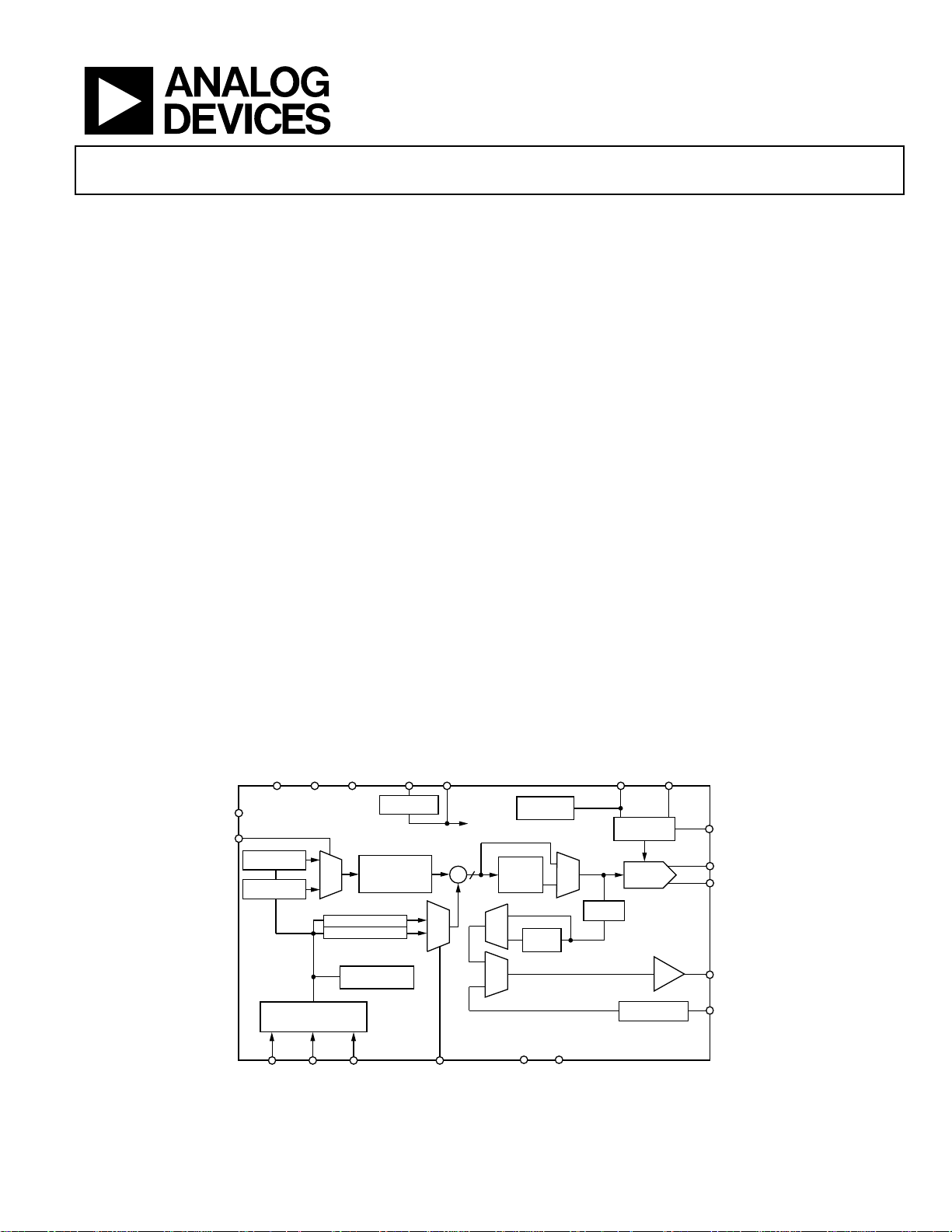
FUNCTIONAL BLOCK DIAGRAM
DGND
CAP/2.5VDVDDAGNDAVDD
75 MHz Complete DDS
AD9834
Capability for phase modulation and frequency modulation is
provided. The frequency registers are 28 bits; with a 75 MHz clock
rate, resolution of 0.28 Hz can be achieved. Similarly, with a 1 MHz
clock rate, the AD9834 can be tuned to 0.004 Hz resolution.
Frequency and phase modulation are affected by loading registers
through the serial interface and toggling the registers using
software or the FSELECT pin and PSELECT pin, respectively.
The AD9834 is written to using a 3-wire serial interface. This
serial interface operates at clock rates up to 40 MHz and is
compatible with DSP and microcontroller standards.
The device operates with a power supply from 2.3 V to 5.5 V.
The analog and digital sections are independent and can be run
from different power supplies, for example, AVDD can equal
5 V with DVDD equal to 3 V.
The AD9834 has a power-down pin (SLEEP) that allows
external control of the power-down mode. Sections of the
device that are not being used can be powered down to
minimize the current consumption. For example, the DAC can
be powered down when a clock output is being generated.
The part is available in a 20-lead TSSOP.
REFOUT FS ADJUST
MCLK
FSELECT
28-BIT FREQ0
REG
28-BIT FREQ1
REG
SERIAL I NTERFACE
FSYNC SCLK SDATA
Rev. C
Information furnished by Analog Devices is believed to be accurate and reliable. However, no
responsibility is assumed by Anal og Devices for its use, nor for any infringements of patents or ot her
rights of third parties that may result from its use. Specifications subject to change without notice. No
license is granted by implication or otherwise under any patent or patent rights of Analog Devices.
Trademarks and registered trademarks are the property of their respective owners.
MUX
12-BIT PHASE 0 REG
12-BIT PHASE 1 REG
AND
CONTROL L OGIC
REGULATO R
PHASE
ACCUMULATOR
(28-BIT)
16-BIT CONT ROL
REGISTER
Σ
MUX
VCC
2.5V
12
MUX
MUX
Figure 1.
ON-BOARD
REFERENCE
SIN
ROM
SLEEP RESETPSELECT
MUX
DIVIDED
BY 2
One Technology Way, P.O. Box 9106, Norwood, MA 02062-9106, U.S.A.
Tel: 781.329.4700 www.analog.com
Fax: 781.461.3113 ©2003–2011 Analog Devices, Inc. All rights reserved.
MSB
FULL-SCALE
CONTROL
10-BIT
DAC
COMPARATOR
AD9834
COMP
IOUT
IOUTB
SIGN BIT OUT
VIN
02705-001

AD9834
TABLE OF CONTENTS
Features.............................................................................................. 1
Control Register ......................................................................... 18
Applications....................................................................................... 1
General Description ......................................................................... 1
Functional Block Diagram .............................................................. 1
Revision History ............................................................................... 3
Specifications..................................................................................... 4
Timing Characteristics ................................................................ 6
Absolute Maximum Ratings............................................................ 7
ESD Caution.................................................................................. 7
Pin Configuration and Function Descriptions............................. 8
Typical Performance Characteristics ........................................... 10
Terminology ....................................................................................14
Theory of Operation ...................................................................... 15
Circuit Description......................................................................... 16
Numerically Controlled Oscillator Plus Phase Modulator... 16
SIN ROM..................................................................................... 16
Frequency and Phase Registers ................................................ 20
Writing to a Frequency Register............................................... 21
Writing to a Phase Register....................................................... 21
RESET Function......................................................................... 21
SLEEP Function.......................................................................... 21
SIGN BIT OUT Pin.................................................................... 22
The IOUT and IOUTB Pins...................................................... 22
Applications Information.............................................................. 23
Grounding and Layout .................................................................. 26
Interfacing to Microprocessors..................................................... 27
AD9834 to ADSP-21xx Interface ............................................. 27
AD9834 to 68HC11/68L11 Interface....................................... 27
AD9834 to 80C51/80L51 Interface.......................................... 28
AD9834 to DSP56002 Interface ............................................... 28
Evaluation Board............................................................................ 29
Digital-to-Analog Converter (DAC) ....................................... 16
Comparator................................................................................. 16
Regulator...................................................................................... 17
Output Voltage Compliance...................................................... 17
Functional Description.................................................................. 18
Serial Interface ............................................................................ 18
Powering Up the AD9834 ......................................................... 18
Latency......................................................................................... 18
System Development Platform................................................. 29
AD9834 to SPORT Interface..................................................... 29
XO vs. External Clock................................................................ 29
Power Supply............................................................................... 29
Evaluation Board Schematics ................................................... 30
Evaluation Board Layout........................................................... 32
Outline Dimensions....................................................................... 35
Ordering Guide .......................................................................... 35
Rev. C | Page 2 of 36

AD9834
REVISION HISTORY
2/11—Rev. B to Rev. C
Changes to I
Changes to FS ADJUST Description, Table 4................................8
Added Output Voltage Compliance Section................................17
Changes to Figure 31 ......................................................................23
Changes to Figure 32 ......................................................................24
Deleted Using the AD9834 Evaluation Board Section and the
Prototyping Area Section...............................................................28
Added System Development Platform Section, AD9834 to
SPORT Interface Section, Figure 39, and Figure 40;
Renumbered Sequentially ..............................................................29
Changes to XO vs. External Clock Section and Power Supply
Section ..............................................................................................29
Deleted Bill of Materials, Table 19;
Renumbered Sequentially ..............................................................30
Added Evaluation Board Schematics Section and Figure 41 ....30
Added Figure 42 ..............................................................................31
Added Evaluation Board Layout Section and Figure 43............32
Added Figure 44 ..............................................................................33
Added Figure 45 ..............................................................................34
Changes to Ordering Guide...........................................................35
Parameter, Table 1 ..................................................5
DD
4/10—Rev. A to Rev. B
Changes to Comparator Section ...................................................15
Added Figure 28..............................................................................16
Changes to Serial Interface Section ..............................................17
8/06—Rev. 0 to Rev. A
Updated Format ................................................................. Universal
Changed to 75 MHz Complete DDS ............................... Universal
Changes to Features Section............................................................1
Changes to Table 1 ............................................................................4
Changes to Table 2 ............................................................................6
Changes to Table 3 ............................................................................8
Added Figure 10, Figures Renumbered Sequentially................... 9
Added Figure 16 and Figure 17, Figures Renumbered
Sequentially......................................................................................10
Changes to Table 6 ..........................................................................19
Changes to Writing a Frequency Register Section .....................20
Changes to Figure 29 ......................................................................21
Changes to Table 19 ........................................................................30
Changes to Figure 38 ......................................................................28
2/03—Revision 0: Initial Version
Rev. C | Page 3 of 36

AD9834
SPECIFICATIONS
VDD = 2.3 V to 5.5 V, AGND = DGND = 0 V, TA = T
Table 1.
Grade B, Grade C1
Parameter2 Min Typ Max Unit Test Conditions/Comments
SIGNAL DAC SPECIFICATIONS
Resolution 10 Bits
Update Rate 75 MSPS
I
Full Scale3 3.0 mA
OUT
V
Max 0.6 V
OUT
V
Min 30 mV
OUT
Output Compliance4 0.8 V
DC Accuracy
Integral Nonlinearity ±1 LSB
Differential Nonlinearity ±0.5 LSB
DDS SPECIFICATIONS
Dynamic Specifications
Signal-to-Noise Ratio 55 60 dB f
Total Harmonic Distortion −66 −56 dBc f
Spurious-Free Dynamic Range (SFDR)
Wideband (0 to Nyquist) −60 −56 dBc f
Narrow Band (±200 kHz)
B Grade −78 −67 dBc f
C Grade −74 −65 dBc f
Clock Feedthrough −50 dBc
Wake-Up Time 1 ms
COMPARATOR
Input Voltage Range 1 V p-p AC-coupled internally
Input Capacitance 10 pF
Input High-Pass Cutoff Frequency 4 MHz
Input DC Resistance 5 MΩ
Input Leakage Current 10 A
OUTPUT BUFFER
Output Rise/Fall Time 12 ns Using a 15 pF load
Output Jitter 120 ps rms 3 MHz sine wave, 0.6 V p-p
VOLTAGE REFERENCE
Internal Reference 1.12 1.18 1.24 V
REFOUT Output Impedance5 1 kΩ
Reference Temperature Coefficient 100 ppm/°C
LOGIC INPUTS
Input High Voltage, V
1.7 V 2.3 V to 2.7 V power supply
INH
2.0 V 2.7 V to 3.6 V power supply
2.8 V 4.5 V to 5.5 V power supply
Input Low Voltage, V
0.6 V 2.3 V to 2.7 V power supply
INL
0.7 V 2.7 V to 3.6 V power supply
0.8 V 4.5 V to 5.5 V power supply
Input Current, I
10 µA
INH/IINL
Input Capacitance, CIN 3 pF
MIN
to T
MAX
, R
SET
= 6.8 k, R
= 200 for IOUT and IOUTB, unless otherwise noted.
LOAD
= 75 MHz, f
MCLK
= 75 MHz, f
MCLK
= 75 MHz, f
MCLK
= 50 MHz, f
MCLK
= 75 MHz, f
MCLK
OUT
OUT
OUT
OUT
OUT
= f
= f
= f
= f
= f
MCLK
MCLK
MCLK
MCLK
MCLK
/4096
/4096
/75
/50
/75
Rev. C | Page 4 of 36
AD9834
F
Grade B, Grade C1
Parameter2 Min Typ Max Unit Test Conditions/Comments
POWER SUPPLIES
AVDD 2.3 5.5 V f
DVDD 2.3 5.5 V
6
I
3.8 5 mA
AA
6
I
DD
B Grade 2.0 3 mA IDD code dependent (see Figure 8)
C Grade 2.7 3.7 mA IDD code dependent (see Figure 8)
6
IAA + I
DD
B Grade 5.8 8 mA
C Grade 6.5 8.7 mA
Low Power Sleep Mode
B Grade 0.5 mA DAC powered down, MCLK running
C Grade 0.6 mA DAC powered down, MCLK running
1
B grade: MCLK = 50 MHz; C grade: MCLK = 75 MHz. For specifications that do not specify a grade, the value applies to both grades.
2
Operating temperature range is as follows: B, C versions: −40°C to +105°C, typical specifications are at 25°C.
3
For compliance, with specified load of 200 Ω, I
4
Guaranteed by design.
5
Applies when REFOUT is sourcing current. The impedance is higher when REFOUT is sinking current.
6
Measured with the digital inputs static and equal to 0 V or DVDD.
100n
full scale should not exceed 4 mA.
OUT
10nF
R
SET
6.8kΩ
= 75 MHz, f
MCLK
OUT
= f
MCLK
/4096
ON-BOARD
REFERENCE
12
SIN
ROM
REFOUT
FULL-SCAL E
CONTROL
10-BIT DAC
CAP/2.5V
REGULATOR
AD9834
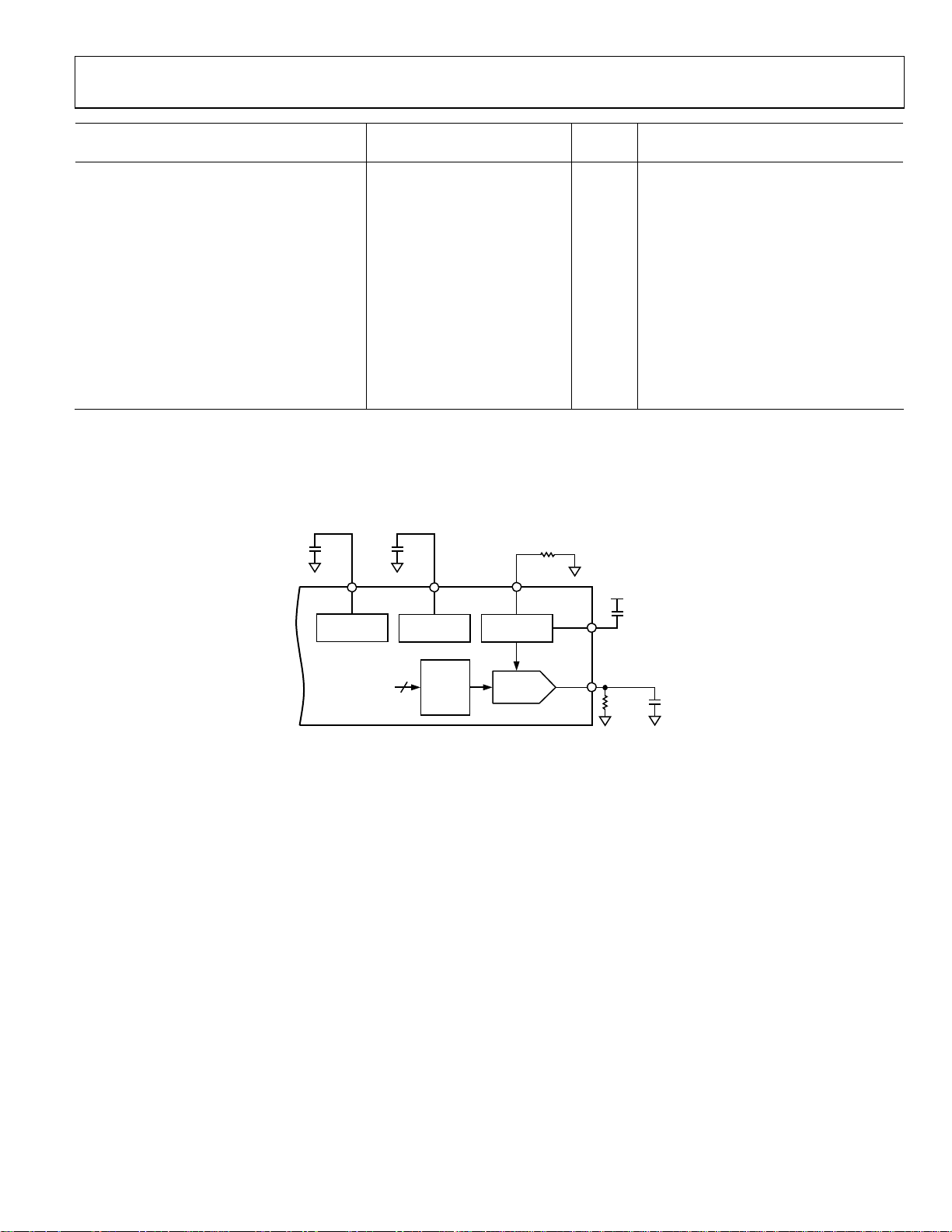
Figure 2. Test Circuit Used to Test the Specifications
FS ADJUST
COMP
IOUT
AVDD
R
LOAD
200Ω
10nF
20pF
02705-002
Rev. C | Page 5 of 36
AD9834
TIMING CHARACTERISTICS
DVDD = 2.3 V to 5.5 V, AGND = DGND = 0 V, unless otherwise noted.
Table 2.
Parameter1 Limit at T
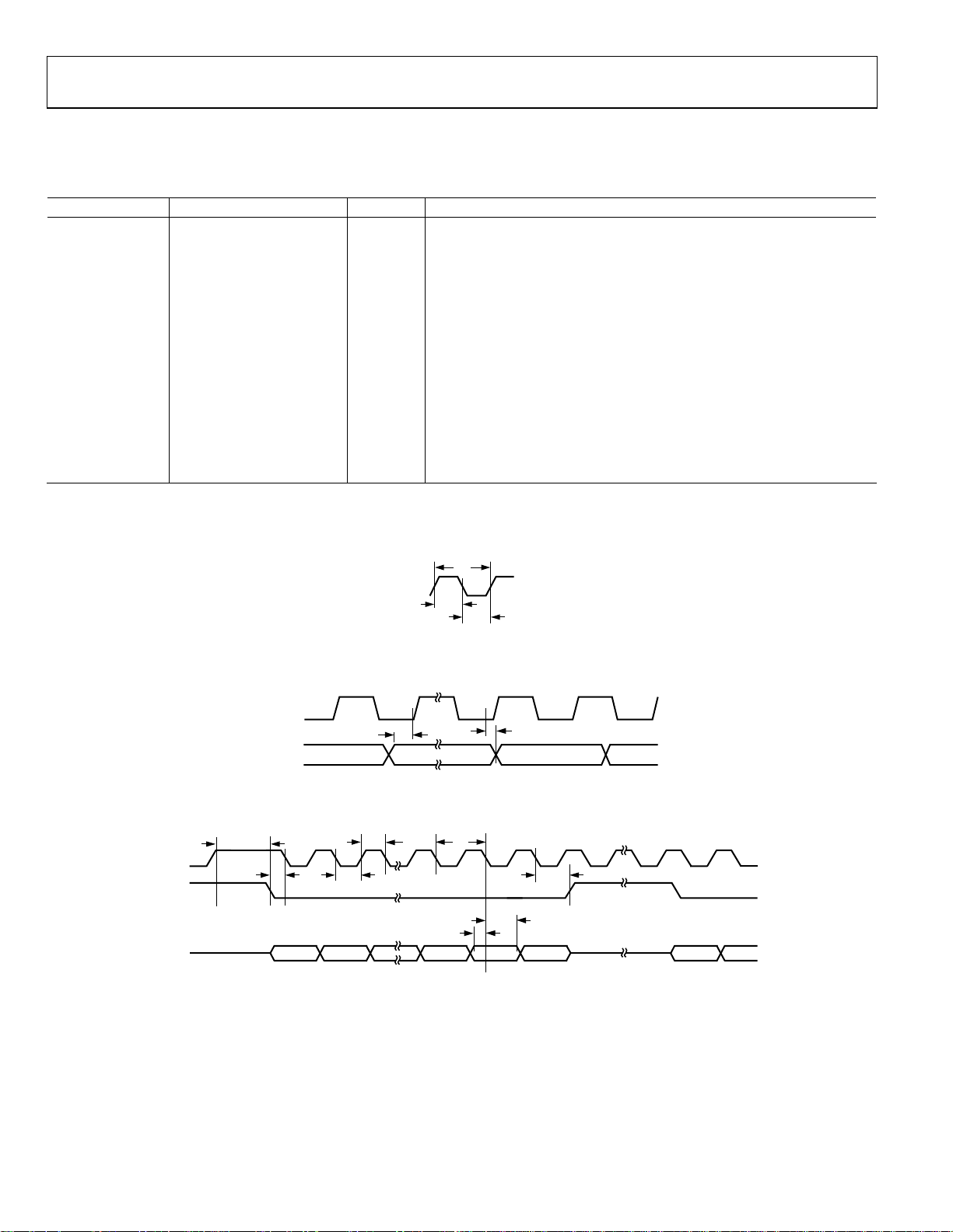
t1 20/13.33 ns min MCLK period: 50 MHz/75 MHz
t2 8/6 ns min MCLK high duration: 50 MHz/75 MHz
t3 8/6 ns min MCLK low duration: 50 MHz/75 MHz
t4 25 ns min SCLK period
t5 10 ns min SCLK high duration
t6 10 ns min SCLK low duration
t7 5 ns min FSYNC-to-SCLK falling edge setup time
t
10 ns min FSYNC-to-SCLK hold time
8 MIN
t
t4 − 5 ns max
8 MAX
t9 5 ns min Data setup time
t10 3 ns min Data hold time
t11 8 ns min FSELECT, PSELECT setup time before MCLK rising edge
t
8 ns min FSELECT, PSELECT setup time after MCLK rising edge
11A
t12 5 ns min SCLK high to FSYNC falling edge setup time
1
Guaranteed by design, not production tested.
MIN
to T
Unit Test Conditions/Comments
MAX
Timing Diagrams
SCLK
FSYNC
SDATA
t
12
t
1
MCLK
t
2
t
3
02705-003
Figure 3. Master Clock
MCLK
t
11A
FSELECT,
PSELECT
t
11
VALID DATA VALID DATA VAL ID DATA
Figure 4. Control Timing
t
5
t
7
D15 D14 D2 D1 D15 D14
t
6
t
4
t
8
t
10
t
9
D0
Figure 5. Serial Timing
02705-004
02705-005
Rev. C | Page 6 of 36
AD9834
ABSOLUTE MAXIMUM RATINGS
TA = 25°C, unless otherwise noted.
Table 3.
Parameter Ratings
AVDD to AGND −0.3 V to +6 V
DVDD to DGND −0.3 V to +6 V
AVDD to DVDD −0.3 V to +0.3 V
AGND to DGND −0.3 V to +0.3 V
CAP/2.5V 2.75 V
Digital I/O Voltage to DGND −0.3 V to DVDD + 0.3 V
Analog I/O Voltage to AGND −0.3 V to AVDD + 0.3 V
Operating Temperature Range
Industrial (B Version) −40°C to +105°C
Storage Temperature Range −65°C to +150°C
Maximum Junction Temperature 150°C
TSSOP Package
θJA Thermal Impedance 143°C/W
θJC Thermal Impedance 45°C/W
Lead Temperature, Soldering (10 sec) 300°C
IR Reflow, Peak Temperature 220°C
Reflow Soldering (Pb-Free)
Peak Temperature 260°C (+0/–5)
Time at Peak Temperature 10 sec to 40 sec
Stresses above those listed under Absolute Maximum Ratings
may cause permanent damage to the device. This is a stress
rating only; functional operation of the device at these or any
other conditions above those indicated in the operational
section of this specification is not implied. Exposure to absolute
maximum rating conditions for extended periods may affect
device reliability.
ESD CAUTION
Rev. C | Page 7 of 36
AD9834
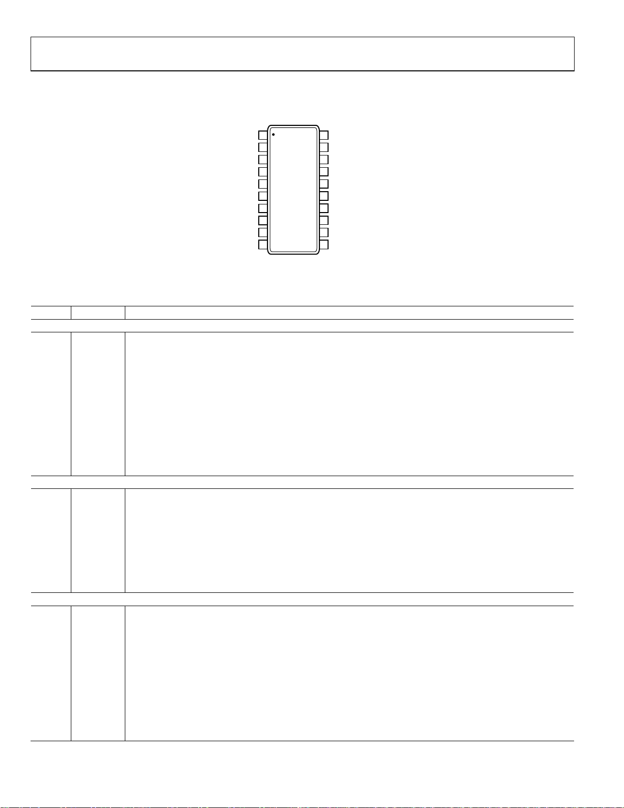
PIN CONFIGURATION AND FUNCTION DESCRIPTIONS
FS ADJUST
REFOUT
COMP
AVD D
DVDD
CAP/2.5V
DGND
MCLK
FSELECT
PSELECT
1
2
3
AD9834
4
TOP VIEW
(Not to Scale)
5
6
7
8
9
10
20
IOUTB
19
IOUT
18
AGND
17
VIN
16
SIGN BIT OUT
15
FSYNC
14
SCLK
13
SDATA
12
SLEEP
11
RESET
02705-006
Figure 6. Pin Configuration
Table 4. Pin Function Descriptions
Pin No. Mnemonic Description
ANALOG SIGNAL AND REFERENCE
1 FS ADJUST
Full-Scale Adjust Control. A resistor (R
of the full-scale DAC current. The relationship between R
IOUT
= 18 × FSADJUST/R
FULL SCALE
FSADJUST = 1.15 V nominal, R
) is connected between this pin and AGND. This determines the magnitude
SET
SET
= 6.8 kΩ typical.
SET
and the full-scale current is as follows:
SET
2 REFOUT Voltage Reference Output. The AD9834 has an internal 1.20 V reference that is made available at this pin.
3 COMP DAC Bias Pin. This pin is used for decoupling the DAC bias voltage.
17 VIN
Input to Comparator. The comparator can be used to generate a square wave from the sinusoidal DAC output. The
DAC output should be filtered appropriately before being applied to the comparator to improve jitter. When Bit
OPBITEN and Bit SIGN/PIB in the control register are set to 1, the comparator input is connected to VIN.
19, 20
IOUT,
IOUTB
Current Output. This is a high impedance current source. A load resistor of nominally 200 Ω should be connected
between IOUT and AGND. IOUTB should preferably be tied through an external load resistor of 200 Ω to AGND, but
it can be tied directly to AGND. A 20 pF capacitor to AGND is also recommended to prevent clock feedthrough.
POWER SUPPLY
4 AVDD
Positive Power Supply for the Analog Section. AVDD can have a value from 2.3 V to 5.5 V. A 0.1 F decoupling
capacitor should be connected between AVDD and AGND.
5 DVDD
Positive Power Supply for the Digital Section. DVDD can have a value from 2.3 V to 5.5 V. A 0.1 F decoupling
capacitor should be connected between DVDD and DGND.
6 CAP/2.5V
The digital circuitry operates from a 2.5 V power supply. This 2.5 V is generated from DVDD using an on-board
regulator (when DVDD exceeds 2.7 V). The regulator requires a decoupling capacitor of typically 100 nF that is
connected from CAP/2.5 V to DGND. If DVDD is equal to or less than 2.7 V, CAP/2.5 V should be shorted to DVDD.
7 DGND Digital Ground.
18 AGND Analog Ground.
DIGITAL INTERFACE AND CONTROL
8 MCLK
Digital Clock Input. DDS output frequencies are expressed as a binary fraction of the frequency of MCLK. The
output frequency accuracy and phase noise are determined by this clock.
9 FSELECT
Frequency Select Input. FSELECT controls which frequency register, FREQ0 or FREQ1, is used in the phase
accumulator. The frequency register to be used can be selected using Pin FSELECT or Bit FSEL. When Bit FSEL is
used to select the frequency register, the FSELECT pin should be tied to CMOS high or low.
10 PSELECT
Phase Select Input. PSELECT controls which phase register, PHASE0 or PHASE1, is added to the phase accumulator
output. The phase register to be used can be selected using Pin PSELECT or Bit PSEL. When the phase registers are being
controlled by Bit PSEL, the PSELECT pin should be tied to CMOS high or low.
11 RESET
Active High Digital Input. RESET resets appropriate internal registers to zero; this corresponds to an analog output
of midscale. RESET does not affect any of the addressable registers.
12 SLEEP
Active High Digital Input. When this pin is high, the DAC is powered down. This pin has the same function as
Control Bit SLEEP12.
Rev. C | Page 8 of 36

AD9834
Pin No. Mnemonic Description
13 SDATA Serial Data Input. The 16-bit serial data-word is applied to this input.
14 SCLK Serial Clock Input. Data is clocked into the AD9834 on each falling SCLK edge.
15 FSYNC
16
SIGN BIT
OUT
Active Low Control Input. This is the frame synchronization signal for the input data. When FSYNC is taken low, the
internal logic is informed that a new word is being loaded into the device.
Logic Output. The comparator output is available on this pin or, alternatively, the MSB from the NCO can be output
on this pin. Setting Bit OPBITEN in the control register to 1 enables this output pin. Bit SIGN/PIB determines
whether the comparator output or the MSB from the NCO is output on the pin.
Rev. C | Page 9 of 36
AD9834
–
–
TYPICAL PERFORMANCE CHARACTERISTICS
4.0
T
= 25°C
A
3.5
0
AVDD = DVDD = 3V
T
= 25°C
A
–10
3.0
2.5
2.0
(mA)
DD
I
1.5
1.0
0.5
0
0
15 30 45 60
MCLK FREQUENCY (MHz)
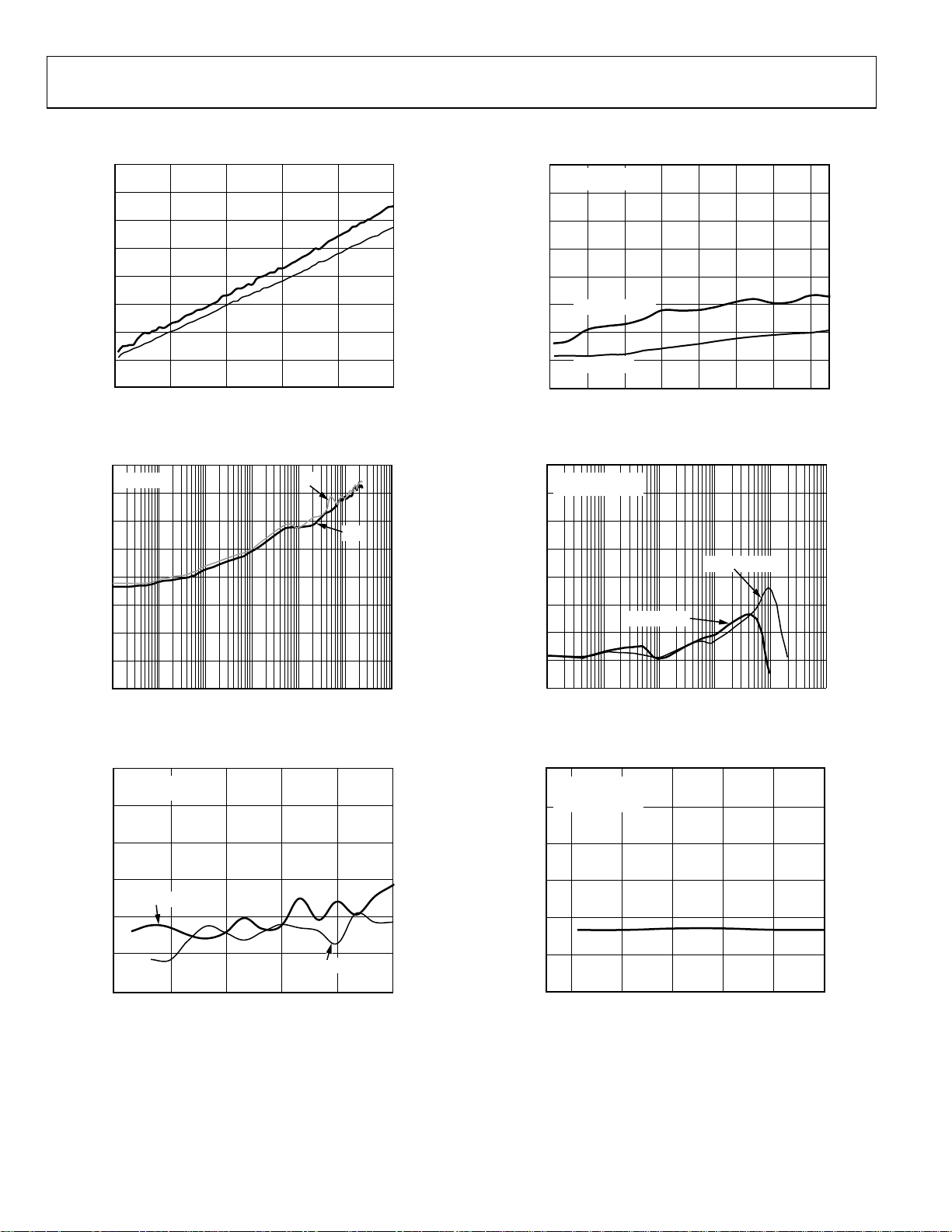
Figure 7. Typical Current Consumption (I
4.0
TA = 25°C
3.5
3.0
2.5
2.0
(mA)
DD
I
1.5
1.0
0.5
5V
3V
) vs. MCLK Frequency
DD
5V
–20
–30
–40
SFDR (dBc)
–50
–60
–70
75
02705-007
–80
SFDR dB MCLK/7
f
= 1MHz
OUT
0 10203040506070
MCLK FREQUENCY (MHz)
02705-010
Figure 10. Wideband SFDR vs. MCLK Frequency
0
AVDD = DVDD = 3V
T
= 25°C
A
–10
3V
–20
–30
–40
SFDR (dBc)
–50
–60
–70
30MHz CLOCK
50MHz CLOCK
0
100 1k 10k 100k 1M 10M 100M
Figure 8. Typical I
60
AVDD = DVDD = 3V
T
= 25°C
A
–65
–70
–75
SFDR dB MCLK/ 50
SFDR (dBc)
–80
–85
–90
01530456075
f
(Hz)
OUT
vs. f
for f
DD
OUT
MCLK
SFDR dB MCLK/7
MCLK FREQUENCY ( MHz)
= 50 MHz
Figure 9. Narrow-Band SFDR vs. MCLK Frequency
–80
0.001 0.01 0.1 1. 0 10 100
02705-008
Figure 11. Wideband SFDR vs. f
40
TA = 25°C
AVDD = DVDD = 3V
= MCLK/4096
f
OUT
–45
–50
–55
SNR (dB)
–60
–65
–70
1.0 5.0 10. 0 12.5 25.0 50.0
02705-009
f
OUT/fMCLK
for Various MCLK Frequencies
OUT/fMCLK
MCLK FREQUENCY ( MHz)
2705-011
02705-012
Figure 12. SNR vs. MCLK Frequency
Rev. C | Page 10 of 36
AD9834
–
1000
950
900
850
800
750
700
WAKE-UP TIME (µs)
650
600
550
500
–40 25 105
5.5V
TEMPERATURE (° C)
2.3V
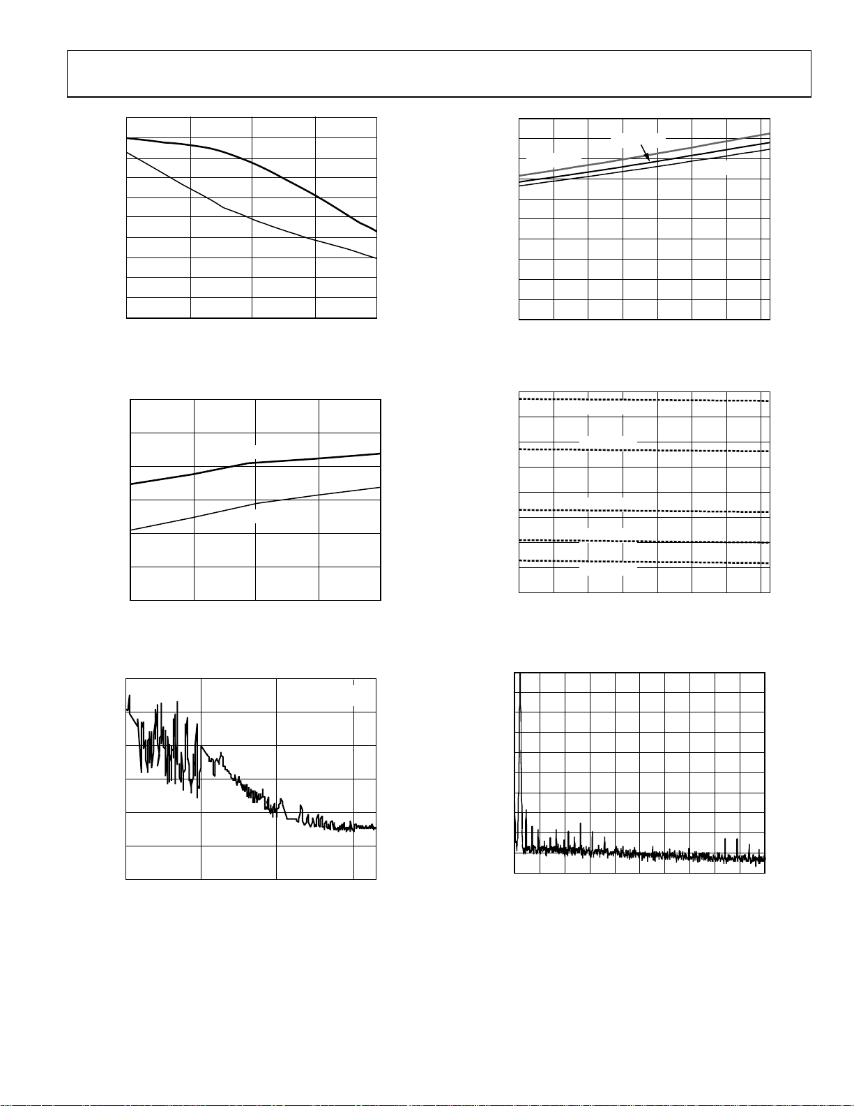
Figure 13. Wake-Up Time vs. Temperature
02705-013
0.20
0.18
0.16
DVDD = 2.3V
0.14
0.12
0.10
DVDD (V)
0.08
0.06
0.04
0.02
0
–40–200 20406080100
Figure 16. SIGN BIT OUT Low Level, I
DVDD = 3.3V
TEMPERATURE (°C)
DVDD = 5.5V
= 1 mA
SINK
02705-037
1.250
1.225
UPPER RANGE
1.200
(V)
1.175
(REFOUT)
V
1.150
1.125
1.100
–40 25 105
Figure 14. V
100
–110
–120
–130
(dBc/Hz)
–140
–150
–160
100 1k 10k 100k 200k
Figure 15. Output Phase Noise, f
LOWER RANGE
TEMPERATURE ( °C)
vs. Temperature
REFOUT
FREQUENCY (Hz)
= 2 MHz, MCLK = 50 MHz
OUT
AVDD = DVDD = 5V
T
= 25°C
A
5.5
5.0
4.5
4.0
3.5
DVDD (V)
3.0
2.5
2.0
1.5
–40–200 20406080100
2705-014
Figure 17. SIGN BIT OUT High Level, I
0
–10
–20
–30
–40
–50
(dB)
–60
–70
–80
–90
–100
0 100k
RWB 100 ST 100 SECVWB 30
02705-015
Figure 18. f
MCLK
DVDD = 5.5V
DVDD = 4.5V
DVDD = 3.3V
DVDD = 2.7V
DVDD = 2.3V
= 10 MHz; f
TEMPERATURE (°C)
= 1 mA
SINK
FREQUENCY (Hz)
= 2.4 kHz, Frequency Word = 000FBA9
OUT
02705-038
02705-016
Rev. C | Page 11 of 36
 Loading...