查询AD9833供应商
PRELIMINAR Y TECHNICAL DA T A
+2.5 V to +5.5 V, 25 MHz Low Power
=
CMOS Complete DDS
Preliminary Technical Data AD9833
FEATURES
+2.3 V to +5.5 V Power Supply
25 MHz Speed
Tiny 10-Pin
µµ
µSOIC Package
µµ
Serial Loading
Sinusoidal/Triangular DAC Output
Power-Down Option
Narrowband SFDR > 72 dB
20 mW Power Consumption at 3 V
APPLICATIONS
Digital Modulation
Portable Equipment
Test Equipment
DDS Tuning
GENERAL DESCRIPTION
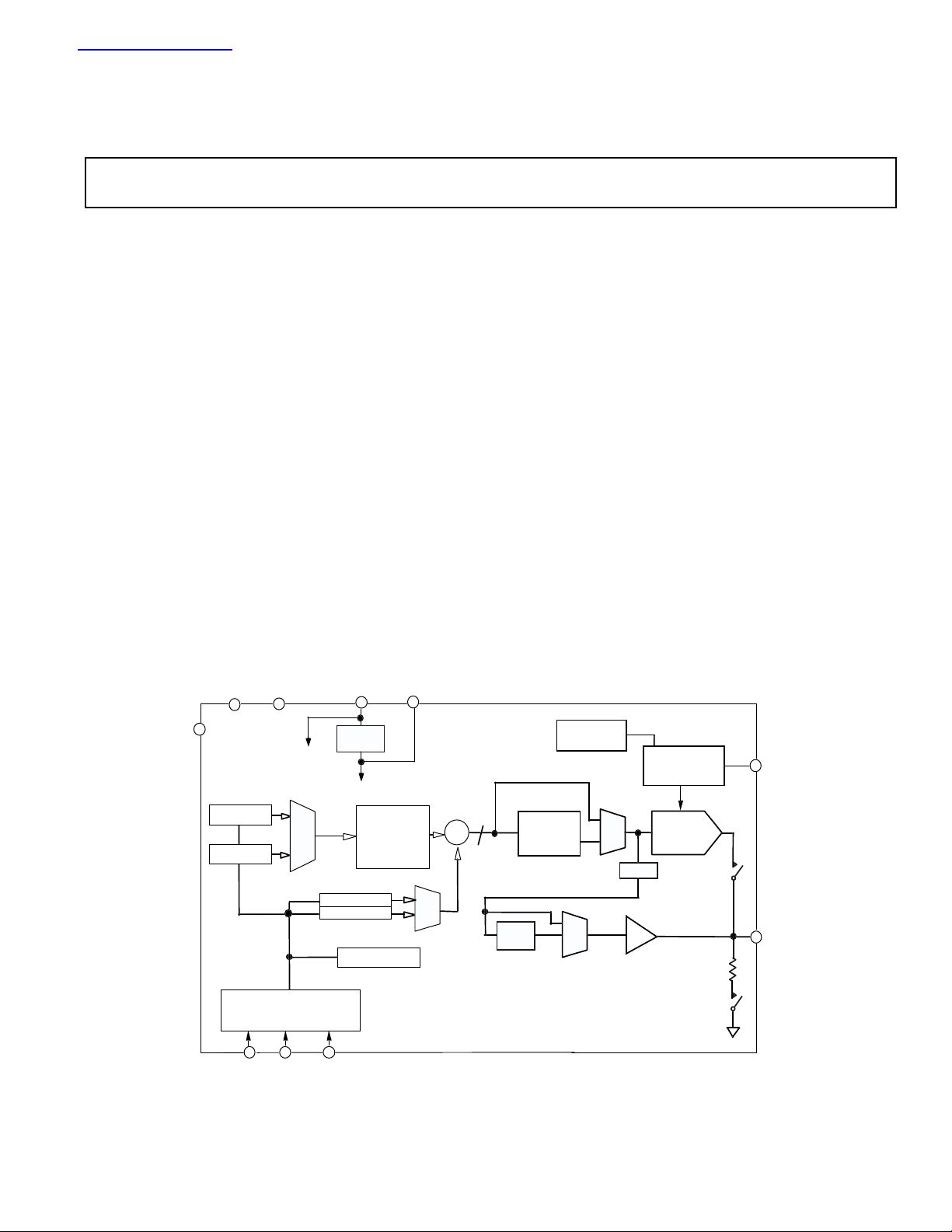
This low power DDS device is a numerically controlled
oscillator employing a phase accumulator, a SIN ROM
and a 10-bit D/A converter integrated on a single
CMOS chip. Clock rates up to 25 MHz are supported
with a power supply from +2.3 V to +5.5 V.
Capability for phase modulation and frequency modula-
tion is provided. Frequency accuracy can be controlled to
one part in 0.25 billion. Modulation is effected by loading
registers through the serial interface.
The AD9833 offers a variety of output waveforms from
the VOUT pin. The SIN ROM can be bypassed so that a
linear up/down ramp is output from the DAC. If the SIN
ROM is not by-passed, a sinusoidal output is available.
Also, if a clock output is required, the MSB of the DAC
data can be output.
The digital section is internally operated at +2.5 V, irrespective of the value of VDD, by an on board regulator
which steps down VDD to +2.5 V, when VDD exceeds
+2.5 V.
The AD9833 has a power-down function (SLEEP). This
allows sections of the device which are not being used to
be powered down, thus minimising the current consumption of the part e.g the DAC can be powered down when a
clock output is being generated.
The AD9833 is available in a 10-pin µSOIC package.
FUNCTIONAL BLOCK DIAGRAM
CAP/2.5V
2.5V
Phase
Accumulator
(28 Bit)
Σ
MUX
MCLK
AGND
FREQ0 REG
FREQ1 REG
FSYNC
DGND
AVDD/
DVDD
MUX
Serial Interface
&
Control Logic
SCLK
SDATA
VDD
Regulator
PHASE0 REG
PHASE1 REG
Control Register
REV PrG 02/02
Information furnished by Analog Devices is believed to be accurate and
reliable. However, no responsibility is assumed by Analog Devices for its
use, nor for any infringements of patents or other rights of third parties
which may result from its use. No license is granted by implication or
otherwise under any patent or patent rights of Analog Devices.
On-Board
Reference
FullScale
Control
12
DIV BY
2
SIN
ROM
MUX
MUX
MSB
10-Bit DAC
200
R
Ω
COMP
VOUT
AD9833
One Technology Way, P.O. Box 9106, Norwood, MA 02062-9106,U.S.A.
Tel: 781/329-4700 www.analog.com
Fax: 781/326-8703 © Analog Devices, Inc., 2002

PRELIMINAR Y TECHNICAL DA TA
AD9833
= 6.8 k
ΩΩ
Ω for
ΩΩ
SPECIFICATIONS
1
(VDD = +2.3 V to +5.5 V; AGND = DGND = 0 V; TA = T
MIN
to T
MAX
; R
SET
VOUT unless otherwise noted)
Parameter Min Typ Max Units Test Conditions/Comments
SIGNAL DAC SPECIFICATIONS
Resolution 10 Bits
Update Rate (f
Output Compliance
) 25 MSPS
MAX
2
0.8 V
DC Accuracy:
Integral Nonlinearity ±1 LSB
Differential Nonlinearity ±0.5 LSB
DDS SPECIFICATIONS
Dynamic Specifications:
Signal to Noise Ratio 50 dB f
Total Harmonic Distortion -53 dBc f
= 25 MHz, f
MCLK
= 25 MHz, f
MCLK
= 1.5 kHz
OUT
= 1.5 kHz
OUT
Spurious Free Dynamic Range (SFDR):
Wideband (± 2 MHz) 50 dBc f
55 dBc f
NarrowBand (± 50 kHz) 72 dBc f
75 dBc f
= 25 MHz, f
MCLK
= 25 MHz, f
MCLK
= 25 MHz, f
MCLK
= 25 MHz, f
MCLK
= f
OUT
= 0.5 MHz
OUT
= f
OUT
= 0.5 MHz
OUT
MCLK
MCLK
/3
/3
Clock Feedthrough –55 dBc
Wake Up Time 1 ms
OUTPUT BUFFER
Output Rise/Fall Time 20 ns Using a 15 pF Load
Output Jitter 100 ps rms When DAC data MSB is output
VOLTAGE REFERENCE
Internal Reference 1.116 1.2 1.284 V 1.2 V ± 7%
LOGIC INPUTS
V
, Input High Voltage VDD –0.9 V +3.6 V to +5.5 V Power Supply
INH
- 0.5 V +2.7 V to +3.6 V Power Supply
V
DD
2 V +2.3 V to + 2.7 V Power Supply
V
, Input Low Voltage 0.9 V +3.6 V to +5.5 V Power Supply
INL
0.5 V +2.3 V to + 3.6 V Power Supply
, Input Current 1 µA
I
INH
CIN, Input Capacitance 10 pF
POWER SUPPLIES f
VDD 2.3 5.5 V
3
I
AA
3
I
DD
I
AA
Low Power Sleep Mode
NOTES
1
Operating temperature range is as follows: B Version: –40°C to +85°C; typical specifications are at 25ⴗC
2
Guaranteed by Design.
3
Measured with the digital inputs static and equal to 0 V or DVDD.
Specifications subject to change without notice. There is 95% test coverage of the digital circuitry.
+ I
DD
3
3
1 + 0.04/MHz mA
7 10 mA 3 V Power Supply
10 15 mA 5 V Power Supply
0.25 mA DAC and Internal Clock Powered Down
5mA
= 25 MHz, f
MCLK
OUT
= f
MCLK
/7
–2– REV PrG

PRELIMINAR Y TECHNICAL DA T A
AD9833
100nF
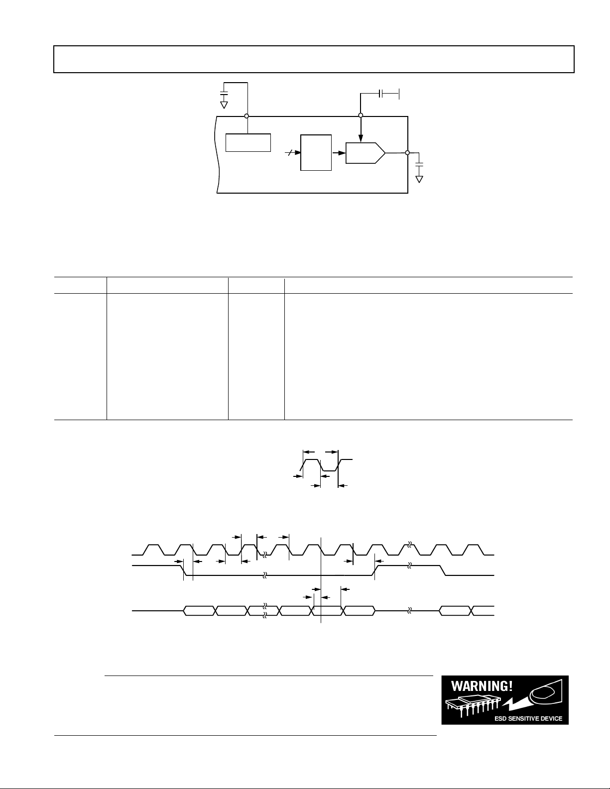
Figure 1. Test Circuit With which Specifications are tested.
TIMING CHARACTERISTICS
Parameter Limit at T
t
1
t
2
t
3
t
4
t
5
t
6
t
7
t
8
t
9
t
10
1
Guaranteed by design, not production tested.
40 ns min MCLK Period
16 ns min MCLK High Duration
16 ns min MCLK Low Duration
25 ns min SCLK Period
10 ns min SCLK High Duration
10 ns min SCLK Low Duration
5 ns min FSYNC to SCLK Falling Edge Setup Time
10 ns min FSYNC to SCLK Hold Time
- 5 ns max
t
4
5 ns min Data Setup Time
3 ns min Data Hold Time
MIN
to T
MAX
VDD
10nF
CAP/2.5V
REGULATOR
12
SIN
ROM
COMP
10-BIT DAC
VOUT
20pF
AD9833
1
(VDD = +2.3 V to +5.5 V; AGND = DGND = 0 V, unless otherwise noted)
Units Test Conditions/Comments
t
1
MCLK
t
2
t
3
Figure 2. Master Clock
t
t
5
4
SCLK
FSYNC
SDATA
t
7
D15 D14 D2 D1 D0 D15 D14
t
6
t
10
t
9
t
8
Figure 3. Serial Timing
CAUTION
ESD (electrostatic discharge) sensitive device. Electrostatic charges as high as 4000 V readily
accumulate on the human body and test equipment and can discharge without detection.
Although the AD9833 features proprietary ESD protection circuitry, permanent damage may
occur on devices subjected to high energy electrostatic discharges. Therefore, proper ESD
precautions are recommended to avoid performance degradation or loss of functionality.
REV PrG
–3–

PRELIMINAR Y TECHNICAL DA TA
AD9833
ABSOLUTE MAXIMUM RATINGS*
(TA = +25°C unless otherwise noted)
VDD to AGND . . . . . . . . . . . . . . . . . . . . . –0.3 V to +6 V
VDD to DGND . . . . . . . . . . . . . . . . . . . . . –0.3 V to +6 V
AGND to DGND. . . . . . . . . . . . . . . . . . –0.3 V to +0.3 V
CAP/2.5V . . . . . . . . . . . . . . . . . . . . . . . . . . . . . . . . . . 2.75 V
Digital I/O Voltage to DGND . –0.3 V to VDD + 0.3 V
Analog I/O Voltage to AGND . –0.3 V to VDD + 0.3 V
Operating Temperature Range
Industrial (B Version) . . . . . . . . . . . . . .–40°C to +85°C
Maximum Junction Temperature . . . . . . . . . . . . . . 150°C
µSOIC Package
Thermal Impedance . . . . . . . . . . . . . . . . . . .206°C/W
θ
JA
θ
Thermal Impedance . . . . . . . . . . . . . . . . . . .44°C/W
JC
Lead Temperature, Soldering (10 sec) . . . . . . . . . 300°C
IR Reflow, Peak Temperature . . . . . . . . . . . . . . . 220°C
*Stresses above those listed under “Absolute Maximum Ratings” may cause permanent
damage to the device. This is a stress rating only and functional operation of the device
at these or any other conditions above those listed in the operational sections of this
specification is not implied. Exposure to absolute maximum rating conditions for
extended periods may affect device reliability.
Storage Temperature Range . . . . . . . . .–65°C to +150°C
ORDERING GUIDE
Model Temperature Range Package Description Package Option
AD9833BRM –40°C to +85°C 14-Pin µSOIC (
Micro Small Outline IC
) RM-10
EVAL-AD9833EB Evaluation Board
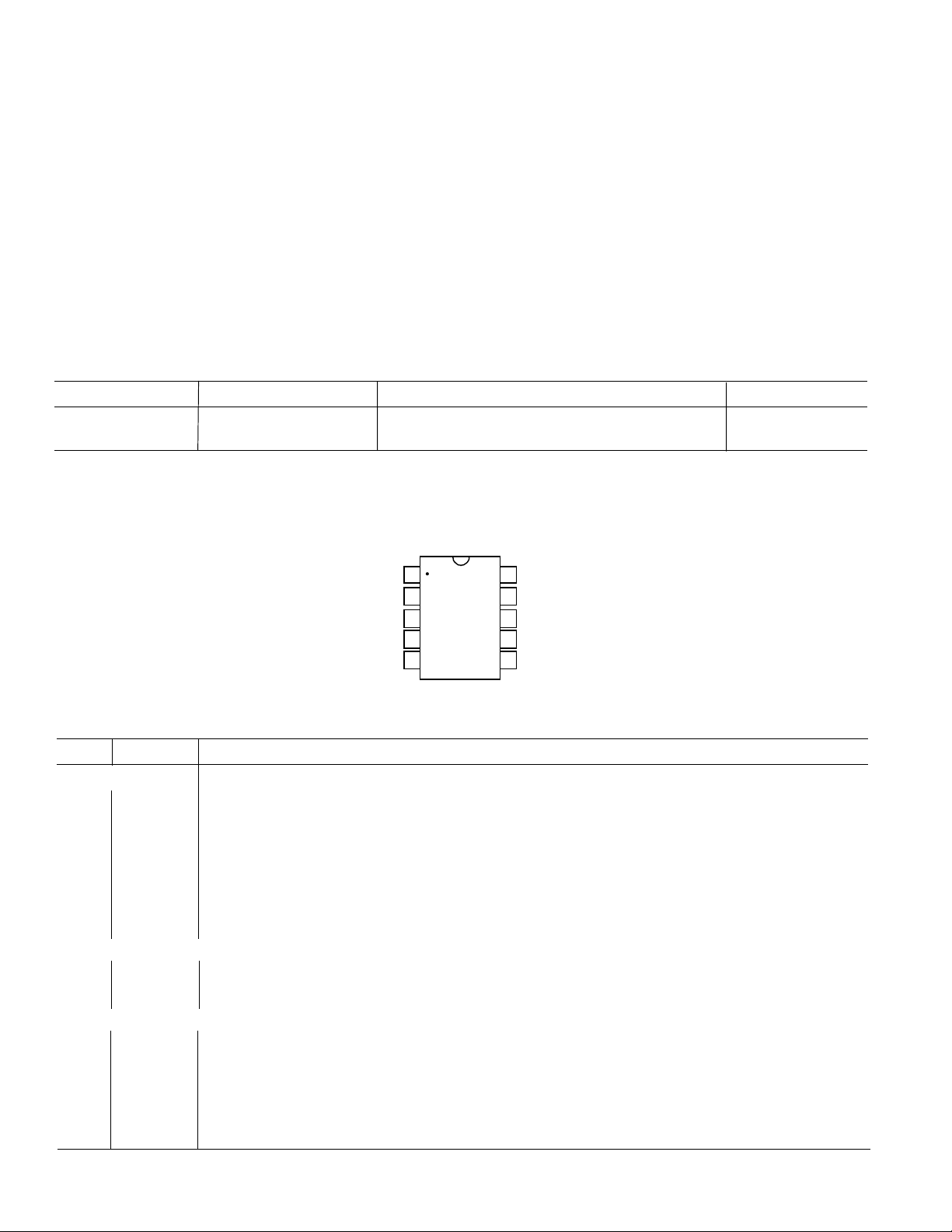
PIN CONFIGURATION
COMP
VDD
CAP/2.5V
DGND
MCLK
1
2
AD9833
3
TOP VIEW
(Notto Scale)
4
5
10
VOUT
9
AGND
8
FSYNC
7
SCLK
6
SDATA
PIN DESCRIPTION
Pin # Mnemonic Function
POWER SUPPLY
2 VDD Positive power supply for the analog section and the digital interface sections. The on board 2.5 V
regulator is also supplied from VDD. VDD can have a value from +2.3 V to +5.5 V. A 0.1 µF and
10 µF decoupling capacitor should be connected between VDD and AGND.
3 CAP/2.5V The digital circuitry operates from a +2.5 V power supply. This +2.5 V is generated from VDD
using an on board regulator (when VDD exceeds +2.7 V). The regulator requires a decoupling
capacitor of typically 100 nF, which is connected from CAP/2.5V to DGND. If VDD is equal to
or less than +2.7 V, CAP/2.5V should be tied directly to VDD.
4 DGND Digital Ground.
9 AGND Analog Ground.
ANALOG SIGNAL AND REFERENCE
1 COMP A DAC Bias Pin. This pin is used for de-coupling the DAC bias voltage.
10 VOUT Voltage Output. The analog and digital output from the AD9833 is available at this pin. An
external load resistor is not required as the device has a 200W resistor on board.
DIGITAL INTERFACE AND CONTROL
5 MCLK Digital Clock Input. DDS output frequencies are expressed as a binary fraction of the frequency of
MCLK. The output frequency accuracy and phase noise are determined by this clock.
6 SDATA Serial Data Input. The 16-bit serial data word is applied to this input.
7 SCLK Serial Clock Input. Data is clocked into the AD9833 on each falling SCLK edge.
8 FSYNC Active Low Control Input. This is the frame synchronisation signal for the input data. When
FSYNC is taken low, the internal logic is informed that a new word is being loaded into the
device.
–4– REV PrG

PRELIMINAR Y TECHNICAL DA T A
Typical Performance Characteristics
AD9833
TBD
TPC 1. Typical Current Consumption
vs. MCLK Frequency
TBD
TPC 4. Wide Band SFDR vs. f
for Various MCLK Frequencies
OUT/fMCLK
TBD
TPC 2. Narrow Band SFDR vs. MCLK
Frequency
TBD
TPC 5. SNR vs. MCLK Frequency
TBD
TPC 3. Wide Band SFDR vs. MCLK
Frequency
TBD
TPC 6. SNR vs. f
Various MCLK Frequencies
OUT/fMCLK
for
TPC 7. Wake-Up Time vs.
REV PrG
TBD
Temperature
–5–

PRELIMINAR Y TECHNICAL DA TA
AD9833
Typical Performance Characteristics
TBD
TPC 9. f
Frequency Word = 000FBA9
= 10 MHz; f
MCLK
OUT
TBD
TPC 12. f
Frequency Word =
= 25 MHz; f
MCLK
= 2.4 kHz;
= 6 kHz;
OUT
000FBA9
TBD
TPC 10. f
Frequency Word = 2492492
= 10 MHz; f
MCLK
= f
MCLK
/7 ;
TBD
TPC 13. f
Frequency Word =
= 25 MHz; f
MCLK
= 1.43 kHz
OUT
= 60 kHz;
OUT
009D495
TBD
TPC 11. f
Frequency Word = 5555555
= 10 MHz; f
MCLK
= f
MCLK
/3 ;
TBD
TPC 14. f
Frequency Word =
= 25 MHz; f
MCLK
= 3.33 kHz
OUT
= 600 kHz;
OUT
0624DD3
TBD
TPC 15. f
f
Frequency Word =
OUT
= 25 MHz;
MCLK
= 2.4 MHz;
189374D
TBD
TPC 16. f
f
= 3.857 MHz = f
OUT
Frequency Word = 277EE4F
= 25 MHz;
MCLK
–6– REV PrG
MCLK
/7 ;
TBD
TPC 17. f
f
= 8.333 MHz = f
OUT
Frequency Word = 555475C
= 25 MHz;
MCLK
MCLK
/3 ;
 Loading...