Analog Devices AD9830AST Datasheet

REV. A
Information furnished by Analog Devices is believed to be accurate and
reliable. However, no responsibility is assumed by Analog Devices for its
use, nor for any infringements of patents or other rights of third parties
which may result from its use. No license is granted by implication or
otherwise under any patent or patent rights of Analog Devices.
a
CMOS
Complete DDS
AD9830
© Analog Devices, Inc., 1996
One Technology Way, P.O. Box 9106, Norwood, MA 02062-9106, U.S.A.
Tel: 617/329-4700 Fax: 617/326-8703
FEATURES
+5 V Power Supply
50 MHz Speed
On-Chip SINE Look-Up Table
On-Chip 10-Bit DAC
Parallel Loading
Power-Down Option
72 dB SFDR
250 mW Power Consumption
48-Pin TQFP
APPLICATIONS
DDS Tuning
Digital Demodulation
GENERAL DESCRIPTION
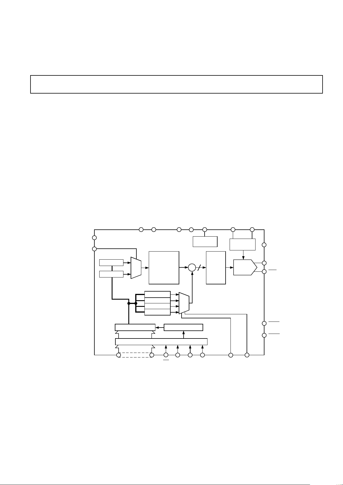
This DDS device is a numerically controlled oscillator employing a phase accumulator, a sine look-up table and a
10-bit D/A converter integrated on a single CMOS chip.
Modulation capabilities are provided for phase modulation
and frequency modulation.
Clock rates up to 50 MHz are supported. Frequency accuracy can be controlled to one part in 4 billion. Modulation
is effected by loading registers through the parallel microprocessor interface.
A power-down pin allows external control of a power-down
mode. The part is available in a 48-pin TQFP package.
FUNCTIONAL BLOCK DIAGRAM
RESET
SLEEP
IOUT
IOUT
COMP
REFINFS ADJUSTREFOUTAGNDAVDD
DGNDDVDD
MCLK
D0
FSELECT
D15
WR
A0 A1 A2 PSEL0 PSEL1
12
AD9830
ON-BOARD
REFERENCE
FULL SCALE
CONTROL
10-BIT DAC
SIN
ROM
PHASE
ACCUMULATOR
(32-BIT)
MUX
MUX
FREQ0 REG
FREQ1 REG
PHASE0 REG
PHASE1 REG
PHASE2 REG
PHASE3 REG
PARALLEL REGISTER TRANSFER CONTROL
MPU INTERFACE
Σ

REV. A
–2–
AD9830–SPECIFICA TIONS
1
Parameter AD9830A Units Test Conditions/Comments
SIGNAL DAC SPECIFICATIONS
Resolution 10 Bits
Update Rate (f
MAX
) 50 MSPS max
I
OUT
Full Scale 20 mA max
Output Compliance 1 V max
DC Accuracy
Integral Nonlinearity ±1 LSB typ
Differential Nonlinearity ± 0.5 LSB typ
DDS SPECIFICATIONS
2
Dynamic Specifications
Signal-to-Noise Ratio 50 dB min f
MCLK
= f
MAX
, f
OUT
= 2 MHz
Total Harmonic Distortion –53 dBc max f
MCLK
= f
MAX
, f
OUT
= 2 MHz
Spurious Free Dynamic Range (SFDR)
3
f
MCLK
= 6.25 MHz, f
OUT
= 2.11 MHz
Narrow Band
(±50 kHz) –72 dBc min
(±200 kHz) –68 dBc min
Wide Band (±2 MHz) –50 dBc min
Clock Feedthrough –55 dBc typ
Wake Up Time 1 ms typ
Power-Down Option Yes
VOLTAGE REFERENCE
Internal Reference @ +25°C 1.21 Volts typ
T
MIN
to T
MAX
1.21 ± 7% Volts min/max
REFIN Input Impedance 10 MΩ typ
Reference TC 100 ppm/°C typ
REFOUT Impedance 300 Ω typ
LOGIC INPUTS
V
INH
, Input High Voltage VDD–0.9 V min
V
INL
, Input Low Voltage 0.9 V max
I
INH
, Input Current 10 µA max
CIN, Input Capacitance 10 pF max
POWER SUPPLIES f
OUT
= 2 MHz
AVDD 4.75/5.25 V min/V max
DVDD 4.75/5.25 V min/V max
I
AA
25 mA max
I
DD
6 + 0.5/MHz mA typ
I
AA
+ I
DD
4
60 mA max
Low Power Sleep Mode
5
0.25 mA typ 1 MΩ Resistor Tied Between
1 mA max REFOUT and AGND
(VDD = +5 V 6 5%; AGND = DGND = 0 V; TA = T
MIN
to T
MAX
; REFIN = REFOUT;
R
SET
= 1 kV; R
LOAD
= 51 V for IOUT and IOUT unless otherwise noted)
NOTES
1
Operating temperature range is as follows: A Version: –40° C to +85°C.
2
All dynamic specifications are measured using IOUT. 100% production tested.
3
f
MCLK
= 6.25 MHz, Frequency Word = 5671C71C HEX, f
OUT
= 2.11 MHz.
4
Measured with the digital inputs static and equal to 0 V or DVDD.
5
The Low Power Sleep Mode current is 2 mA typically when a 1 MΩ resistor is
not tied from REFOUT to AGND.
The AD9830 is tested with a capacitive load of 50 pF. The part can be operated
with higher capacitive loads, but the magnitude of the analog output will be attenuated. For example, a 10 MHz output signal will be attenuated by 3 dB when the
load capacitance equals 250 pF.
Specifications subject to change without notice.
FULL-SCALE
CONTROL
10-BIT
DAC
SIN
ROM
ON-BOARD
REFERENCE
12
REFOUT REFIN FS
ADJUST
COMP
IOUT
IOUT
51Ω
50pF
51Ω
50pF
AVDD
R
SET
1kΩ
10nF
10nF
Figure 1. Test Circuit with Which Specifications Are
Tested

AD9830
REV. A
–3–
TIMING CHARACTERISTICS
Limit at
T
MIN
to T
MAX
Parameter (A Version) Units Test Conditions/Comments
t
1
20 ns min MCLK Period
t
2
8 ns min MCLK High Duration
t
3
8 ns min MCLK Low Duration
t
4
1
8 ns min WR Rising Edge Before MCLK Rising Edge
t
4A
1
8 ns min WR Rising Edge After MCLK Rising Edge
t
5
8 ns min WR Pulse Width
t
6
t
1
ns min Duration Between Consecutive WR Pulses
t
7
5 ns min Data/Address Setup Time
t
8
3 ns min Data/Address Hold Time
t
9
1
8 ns min FSELECT, PSEL0, PSEL1 Setup Time Before MCLK Rising Edge
t
9A
1
8 ns min FSELECT, PSEL0, PSEL1 Setup Time After MCLK Rising Edge
t
10
t
1
ns min RESET Pulse Duration
NOTES
1
See Pin Description section.
Guaranteed by design, but not production tested.
t
1
t
2
t
3
t
4A
t
4
t
5
t
6
MCLK
WR
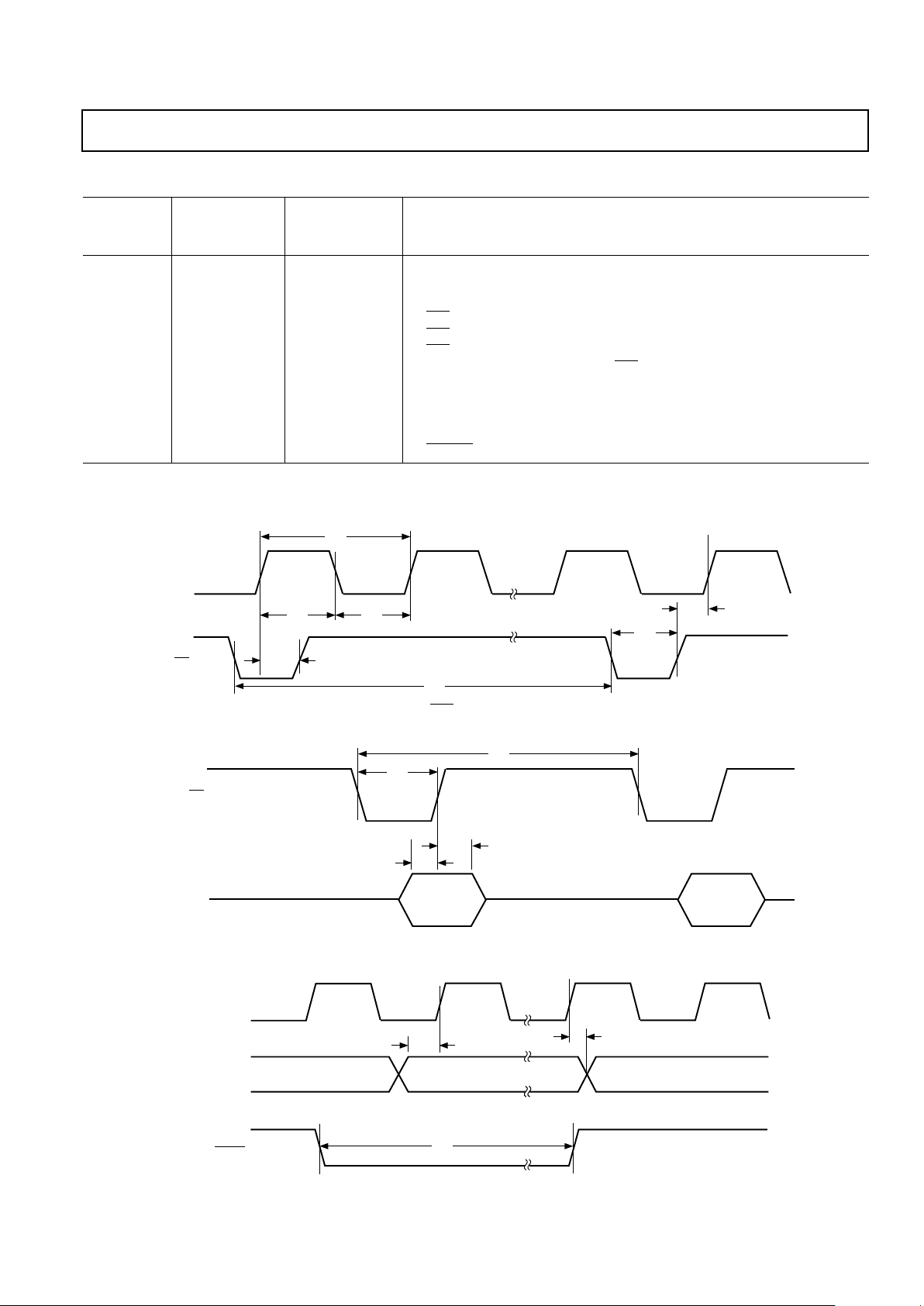
Figure 2.WR–MCLK Relationship
A0, A1, A2
DATA
WR
t
6
t
8
t
7
t
5
VALID DATA VALID DATA
Figure 3. Writing to a Phase/Frequency Register
t
9
VALID DATA VALID DATA VALID DATA
t
9A
t
10
MCLK
FSELECT
PSEL0, PSEL1
RESET
Figure 4. Control Timing
(V
DD
= +5 V 6 5%; AGND = DGND = 0 V, unless otherwise noted)

AD9830
REV. A
–4–
ABSOLUTE MAXIMUM RATINGS*
(
TA = +25°C unless otherwise noted)
AVDD to AGND . . . . . . . . . . . . . . . . . . . . . . . –0.3 V to +7 V
DVDD to DGND . . . . . . . . . . . . . . . . . . . . . . –0.3 V to +7 V
AVDD to DVDD . . . . . . . . . . . . . . . . . . . . . .–0.3 V to +0.3 V
AGND to DGND . . . . . . . . . . . . . . . . . . . . .–0.3 V to +0.3 V
Digital I/O Voltage to DGND . . . . . –0.3 V to DVDD + 0.3 V
Analog I/O Voltage to AGND . . . . . –0.3 V to AVDD + 0.3 V
Operating Temperature Range
Industrial (A Version) . . . . . . . . . . . . . . . . –40°C to +85°C
Storage Temperature Range . . . . . . . . . . . . –65°C to +150°C
Maximum Junction Temperature . . . . . . . . . . . . . . . . +150°C
TQFP θ
JA
Thermal Impedance . . . . . . . . . . . . . . . . . 75°C/W
Lead Temperature, Soldering
Vapor Phase (60 sec) . . . . . . . . . . . . . . . . . . . . . . . +215°C
Infrared (15 sec) . . . . . . . . . . . . . . . . . . . . . . . . . . . +220°C
*Stresses above those listed under “Absolute Maximum Ratings” may cause
permanent damage to the device. This is a stress rating only and functional
operation of the device at these or any other conditions above those listed in the
operational sections of this specification is not implied. Exposure to abso lute
maximum rating conditions for extended periods may affect device reliability.
WARNING!
ESD SENSITIVE DEVICE
CAUTION
ESD (electrostatic discharge) sensitive device. Electrostatic charges as high as 4000 V readily
accumulate on the human body and test equipment and can discharge without detection.
Although this device features proprietary ESD protection circuitry, permanent damage may
occur on devices subjected to high energy electrostatic discharges. Therefore, proper ESD
precautions are recommended to avoid performance degradation or loss of functionality.
ORDERING GUIDE
Model Temperature Range Package Option*
AD9830AST –40°C to +85°C ST-48
*ST = Thin Quad Flatpack (TQFP).
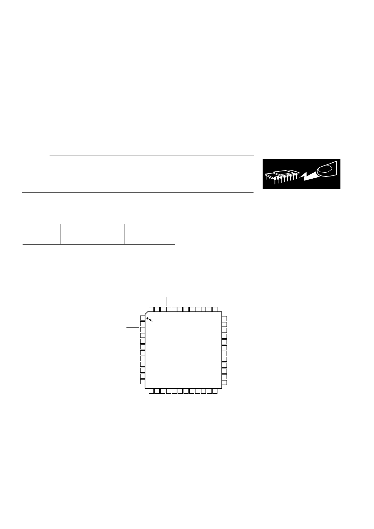
PIN CONFIGURATION
36
35
34
33
32
31
30
29
28
27
26
25
NC
AVDD
FS ADJUST
AGND
NC
AGND
AGND
NC
13 14 15 16 17 18 19 20 21 22 23 24
1
2
3
4
5
6
7
8
9
10
11
12
48 47 46 45 44 39 38 3743 42 41 40
PIN 1
IDENTIFIER
TOP VIEW
(Not to Scale)
AGND
RESET
A0
A1
A2
DB0
DB1
DB11
DGND
DB15
DB14
DB13
DB12
DB10
REFIN
REFOUT
SLEEP
DVDD
DVDD
DGND
MCLK
NC = NO CONNECT
WR
DVDD
FSELECT
PSEL0
DGND
DB2
DB3
DB4
DB9
DB8
DB7
DB6
COMP
AD9830
DB5
PSEL1
DVDD
AVDD
IOUT
IOUT

AD9830
REV. A
–5–
PIN DESCRIPTION
Mnemonic Function
POWER SUPPLY
AVDD Positive power supply for the analog section. A 0.1 µF capacitor should be connected between AVDD and
AGND. AVDD has a value of +5 V ± 5%.
AGND Analog Ground.
DVDD Positive power supply for the digital section. A 0.1 µF decoupling capacitor should be connected between DVDD
and DGND. DVDD has a value of +5 V ± 5%.
DGND Digital Ground.
ANALOG SIGNAL AND REFERENCE
IOUT,
IOUT Current Output. This is a high impedance current source. A load resistor should be connected between IOUT
and AGND.
IOUT should be either tied directly to AGND or through an external load resistor to AGND.
FS ADJUST Full-Scale Adjust Control. A resistor (R
SET
) is connected between this pin and AGND. This determines the mag-
nitude of the full-scale DAC current. The relationship between R
SET
and the full-scale current is as follows:
IOUT
FULL-SCALE
= 16 V
REFIN/RSET
V
REFIN
= 1.21 V nominal, R
SET
= 1 kΩ typical
REFIN Voltage Reference Input. The AD9830 can be used with either the on-board reference, which is available from pin
REFOUT, or an external reference. The reference to be used is connected to the REFIN pin. The AD9830 ac-
cepts a reference of 1.21 V nominal.
REFOUT Voltage Reference Output. The AD9830 has an on-board reference of value 1.21 V nominal. The reference is
made available on the REFOUT pin. This reference is used as the reference to the DAC by connecting REFOUT
to REFIN. REFOUT should be decoupled with a 10 nF capacitor to AGND.
COMP Compensation pin. This is a compensation pin for the internal reference amplifier. A 10 nF decoupling ceramic
capacitor should be connected between COMP and AVDD.
DIGITAL INTERFACE AND CONTROL
MCLK Digital Clock Input. DDS output frequencies are expressed as a binary fraction of the frequency of MCLK. The
output frequency accuracy and phase noise are determined by this clock.
FSELECT Frequency Select Input. FSELECT controls which frequency register, FREQ0 or FREQ1, is used in the phase ac-
cumulator. FSELECT is sampled on the rising MCLK edge. FSELECT needs to be in steady state when an
MCLK rising edge occurs. If FSELECT changes value when an MCLK rising edge occurs, there is an uncertainty
of one MCLK cycle as to when control is transferred to the other frequency register. To avoid any uncertainty, a
change on FSELECT should not coincide with an MCLK rising edge.
WR Write, Edge-Triggered Digital Input. The WR pin is used when writing data to the AD9830. The data is loaded
into the AD9830 on the rising edge of the
WR pulse. This data is then loaded into the destination register on the
MCLK rising edge. The
WR pulse rising edge should not coincide with the MCLK rising edge as there will be an
uncertainty of one MCLK cycle regarding the loading of the destination register with the new data. The
WR rising edge should occur before an MCLK rising edge. The data will then be transferred into the destination register
on the MCLK rising edge. Alternatively, the
WR rising edge can occur after the MCLK rising edge and the desti-
nation register will be loaded on the next MCLK rising edge.
D0–D15 Data Bus, Digital Inputs for destination registers.
A0–A2 Address Digital Inputs. These address bits are used to select the destination register to which the digital data is to
be written.
PSEL0, PSEL1 Phase Select Input. The AD9830 has four phase registers. These registers can be used to alter the value being in-
put to the SIN ROM. The contents of the phase register can be added to the phase accumulator output, the inputs
PSEL0 and PSEL1 selecting the phase register to be used. Like the FSELECT input, the AD9830 samples the
PSEL0 and PSEL1 inputs on the MCLK rising edge. Therefore, these inputs should be in steady state at the
MCLK rising edge or, there is an uncertainty of one MCLK cycle as to when control is transferred to the selected
phase register.
SLEEP Low Power Control, active low digital input. SLEEP puts the AD9830 into a low power mode. Internal clocks
are disabled and the DAC’s current sources and REFOUT are turned off. The AD9830 is re-enabled by taking
SLEEP high.
RESET Reset, active low digital input. RESET resets the phase accumulator to zero which corresponds to an analog
output of midscale.
 Loading...