REV. A
Information furnished by Analog Devices is believed to be accurate and
reliable. However, no responsibility is assumed by Analog Devices for its
use, nor for any infringements of patents or other rights of third parties that
may result from its use. No license is granted by implication or otherwise
under any patent or patent rights of Analog Devices.
a
AD9826
One Technology Way, P.O. Box 9106, Norwood, MA 02062-9106, U.S.A.
Tel: 781/329-4700www.analog.com
Fax: 781/326-8703 © Analog Devices, Inc., 2001
Complete 16-Bit Imaging
Signal Processor
FUNCTIONAL BLOCK DIAGRAM
OEB
DOUT
SCLK
SLOAD
SDATA
ADCCLKCDSCLK2CDSCLK1
OFFSET
VINB
VING
VINR
AVDD AVSS
CML
CAPT
AVDD
AVSS
BANDGAP
REFERENCE
AD9826
DRVDD DRVSS
GAIN
REGISTERS
OFFSET
REGISTERS
3:1
MUX
16:8
MUX
16-BIT
ADC
DIGITAL
CONTROL
INTERFACE
CONFIGURATION
REGISTER
RED
GREEN
BLUE
MUX
REGISTER
8
16
RED
GREEN
BLUE
PGA
6
9
PGA
PGA
CDS
9-BIT
DAC
CDS
9-BIT
DAC
CDS
9-BIT
DAC
INPUT
CLAMP
BIAS
CAPB
FEATURES
16-Bit 15 MSPS A/D Converter
3-Channel 16-Bit Operation up to 15 MSPS
1-Channel 16-Bit Operation up to 12.5 MSPS
2-Channel Mode for Mono Sensors with Odd/Even Outputs
Correlated Double Sampling
1~6ⴛ Programmable Gain
ⴞ300 mV Programmable Offset
Input Clamp Circuitry
Internal Voltage Reference
Multiplexed Byte-Wide Output
Optional Single Byte Output Mode
3-Wire Serial Digital Interface
3 V/5 V Digital I/O Compatibility
28-Lead SSOP Package
Low Power CMOS: 400 mW (Typ)
Power-Down Mode Available
APPLICATIONS
Flatbed Document Scanners
Digital Copier
Multifunction Peripherals
Infrared Imaging Applications
Machine Vision
PRODUCT DESCRIPTION
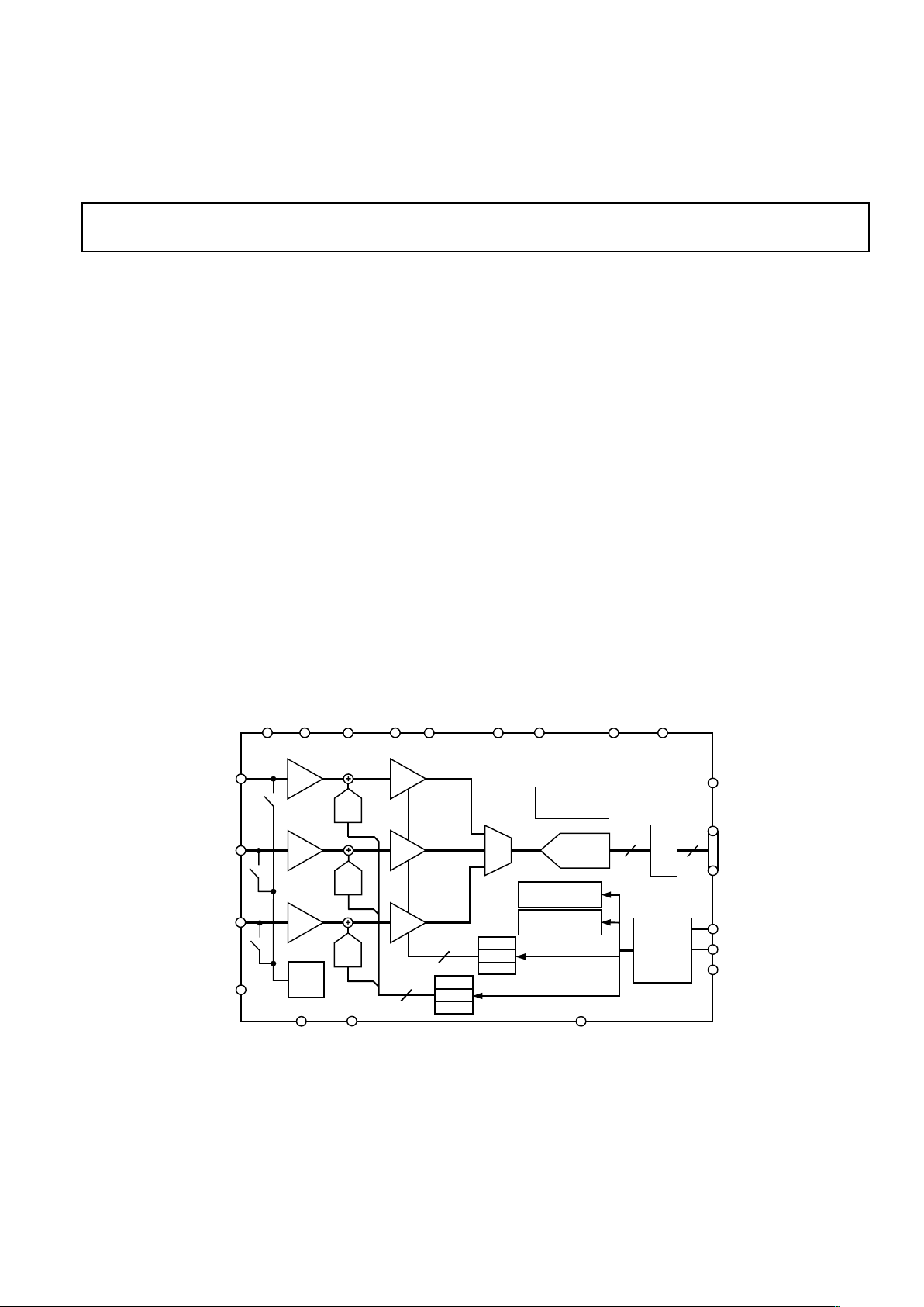
The AD9826 is a complete analog signal processor for imaging
applications. It features a 3-channel architecture designed to
sample and condition the outputs of trilinear color CCD arrays.
Each channel consists of an input clamp, Correlated Double
Sampler (CDS), offset DAC, and Programmable Gain Amplifier
(PGA), multiplexed to a high-performance 16-bit A/D converter.
The AD9826 can operate at speeds greater than 15 MSPS with
reduced performance.
The CDS amplifiers may be disabled for use with sensors that
do not require CDS, such as Contact Image Sensors (CIS),
CMOS active pixel sensors, and Focal Plane Arrays.
The 16-bit digital output is multiplexed into an 8-bit output word,
which is accessed using two read cycles. There is an optional
single byte output mode. The internal registers are programmed
through a 3-wire serial interface, and provide adjustment of
the gain, offset, and operating mode.
The AD9826 operates from a single 5 V power supply, typically
consumes 400 mW of power, and is packaged in a 28-lead SSOP.

–2–
REV. A
AD9826–SPECIFICA TIONS
ANALOG SPECIFICATIONS
Parameter Min Typ Max Unit
MAXIMUM CONVERSION RATE
3-Channel Mode with CDS 30 MSPS
2-Channel Mode with CDS 30 MSPS
1-Channel Mode with CDS 18 MSPS
ACCURACY (ENTIRE SIGNAL PATH)
ADC Resolution 16 Bits
Integral Nonlinearity (INL) ±16 LSB
Differential Nonlinearity (DNL) ±0.5 LSB
No Missing Codes Guaranteed
ANALOG INPUTS
Input Signal Range (Programmable)
1
2.0/4.0 V p-p
Allowable Reset Transient
1
1.0 V
Input Limits
2
AVSS – 0.3 AVDD + 0.3 V
Input Capacitance 10 pF
Input Bias Current 10 nA
AMPLIFIERS
PGA Gain 1 6 V/V
PGA Gain Resolution
2
64 Steps
PGA Gain Monotonicity Guaranteed
Programmable Offset –300 +300 mV
Programmable Offset Resolution 512 Steps
Programmable Offset Monotonicity Guaranteed
NOISE AND CROSSTALK
Total Output Noise @ PGA Minimum 3.0 LSB rms
Total Output Noise @ PGA Maximum 9.0 LSB rms
Channel-to-Channel Crosstalk
@ 15 MSPS 70 dB
@ 6 MSPS 90 dB
POWER SUPPLY REJECTION
AVDD = 5 V 0.25 V 0.1 % FSR
DIFFERENTIAL VREF (at 25°C)
CAPT–CAPB 2.0 V
TEMPERATURE RANGE
Operating –40 +85 °C
Storage –65 +150 °C
POWER SUPPLIES
AVDD 4.75 5.0 5.25 V
DRVDD 3.0 5.0 5.25 V
OPERATING CURRENT
AVDD 75 mA
DRVDD 5 mA
Power-Down Mode 200 µA
POWER DISSIPATION
3-Channel Mode 400 mW
1-Channel Mode 300 mW
NOTES
1
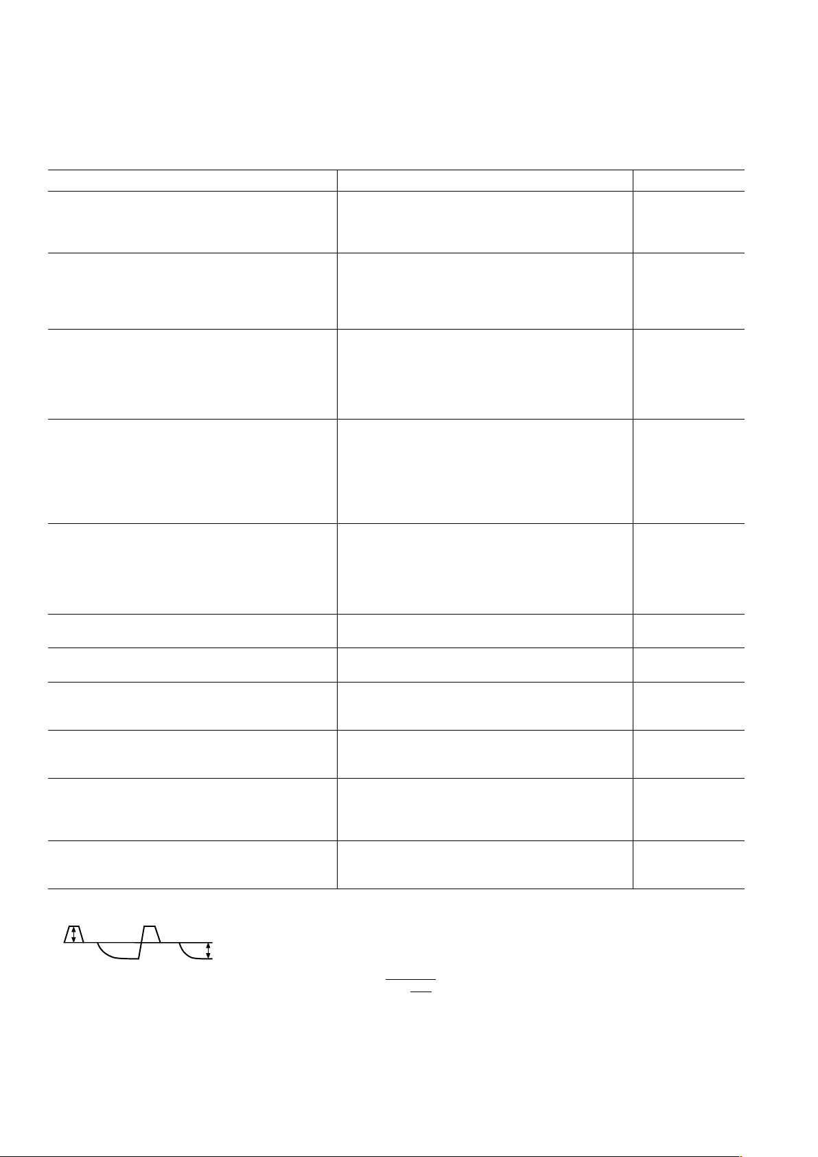
Linear Input Signal Range is from 0 V to 4 V when the CCD’s reference level is clamped to 4 V by the AD9826’s input clamp.
4V SET BY INPUT CLAMP
(3V OPTION ALSO AVAILABLE)
1V TYP
RESET TRANSIENT
4V p-p MAX INPUT SIGNAL RANGE
GND
2
The PGA Gain is approximately “linear in dB” and follows the equation:
G
ain=
6.0
1+5.0
63 – G
63
where G is the register value.
Specifications subject to change without notice.
(T
MIN
to T
MAX
, AVDD = 5 V, DRVDD = 5 V, CDS Mode, f
ADCCLK
= 15 MHz, f
CDSCLK1
= f
CDSCLK2
= 5 MHz, PGA
Gain = 1, Input range = 4 V p-p, unless otherwise noted.)

–3–
REV. A
AD9826
DIGITAL SPECIFICATIONS
Parameter Symbol Min Typ Max Unit
LOGIC INPUTS
High Level Input Voltage V
IH
2.0 V
Low Level Input Voltage V
IL
0.8 V
High Level Input Current I
IH
10 µA
Low Level Input Current I
IL
10 µA
Input Capacitance C
IN
10 pF
LOGIC OUTPUTS
High Level Output Voltage V
OH
4.5 V
Low Level Output Voltage V
OL
0.1 V
High Level Output Current I
OH
50 µA
Low Level Output Current I
OL
50 µA
LOGIC OUTPUTS (with DRVDD = 3 V)
High Level Output Voltage, (I
OH
= 50 µA) V
OH
2.95 V
Low Level Output Voltage (IOL = 50 µA) V
OL
0.05 V
Specifications subject to change without notice.
TIMING SPECIFICATIONS
Parameter Symbol Min Typ Max Unit
CLOCK PARAMETERS
3-Channel Pixel Rate t
PRA
200 ns
1-Channel Pixel Rate t
PRB
80 ns
ADCCLK Pulsewidth t
ADCLK
30 ns
CDSCLK1 Pulsewidth t
C1
8ns
CDSCLK2 Pulsewidth t
C2
8ns
CDSCLK1 Falling to CDSCLK2 Rising t
C1C2
0ns
ADCCLK Falling to CDSCLK2 Rising t
ADC2
0ns
CDSCLK2 Rising to ADCCLK Rising t
C2ADR
5ns
CDSCLK2 Falling to ADCCLK Falling t
C2ADF
30 ns
CDSCLK2 Falling to CDSCLK1 Rising t
C2C1
5ns
Aperture Delay for CDS Clocks t
AD
2ns
SERIAL INTERFACE
Maximum SCLK Frequency f
SCLK
10 MHz
SLOAD to SCLK Set-Up Time t
LS
10 ns
SCLK to SLOAD Hold Time t
LH
10 ns
SDATA to SCLK Rising Set-Up Time t
DS
10 ns
SCLK Rising to SDATA Hold Time t
DH
10 ns
SCLK Falling to SDATA Valid t
RDV
10 ns
DATA OUTPUTS
Output Delay t
OD
6ns
3-State to Data Valid t
DV
10 ns
Output Enable High to 3-State t
HZ
10 ns
Latency (Pipeline Delay) 3 (Fixed) Cycles
NOTES
It is recommended that CDSCLK falling edges do not occur within the first 10 ns following an ADCCLK edge.
Specifications subject to change without notice.
(T
MIN
to T
MAX
, AVDD = 5 V, DRVDD = 5 V, CDS Mode, f
ADCCLK
= 15 MHz, f
CDSCLK1
= f
CDSCLK2
= 5 MHz,
CL = 10 pF, unless otherwise noted.)
(T
MIN
to T
MAX
, AVDD = 5 V, DRVDD = 5 V, specs are for 16-bit performance.)

AD9826
–4–
REV. A
ORDERING GUIDE
Temperature Package Package
Model Range Description Option
AD9826KRS –40°C to +85°C 5.3 mm SSOP RS-28
THERMAL CHARACTERISTICS
Thermal Resistance
28-Lead 5.3 mm SSOP
θ
JA
= 109°C/W
θ
JC
= 39°C/W
ABSOLUTE MAXIMUM RATINGS*
With
Respect
Parameter To Min Max Unit
VIN, CAPT, CAPB AVSS –0.3 AVDD + 0.3 V
Digital Inputs AVSS –0.3 AVDD + 0.3 V
AVDD AVSS –0.5 +6.5 V
DRVDD DRVSS –0.5 +6.5 V
AVSS DRVSS –0.3 +0.3 V
Digital Outputs DRVSS –0.3 DRVDD + 0.3 V
Junction Temperature 150 °C
Storage Temperature –65 +150 °C
Lead Temperature 300 °C
(10 sec)
*Stresses above those listed under Absolute Maximum Ratings may cause perma-
nent damage to the device. This is a stress rating only; functional operation of the
device at these or any other conditions above those listed in the operational
sections of this specification is not implied. Exposure to absolute maximum rating
conditions for extended periods may affect device reliability.
CAUTION
ESD (electrostatic discharge) sensitive device. Electrostatic charges as high as 4000 V readily
accumulate on the human body and test equipment and can discharge without detection. Although
the AD9826 features proprietary ESD protection circuitry, permanent damage may occur on devices
subjected to high-energy electrostatic discharges. Therefore, proper ESD precautions are recommended to avoid performance degradation or loss of functionality.
WARNING!
ESD SENSITIVE DEVICE

AD9826
–5–
REV. A
PIN FUNCTION DESCRIPTIONS
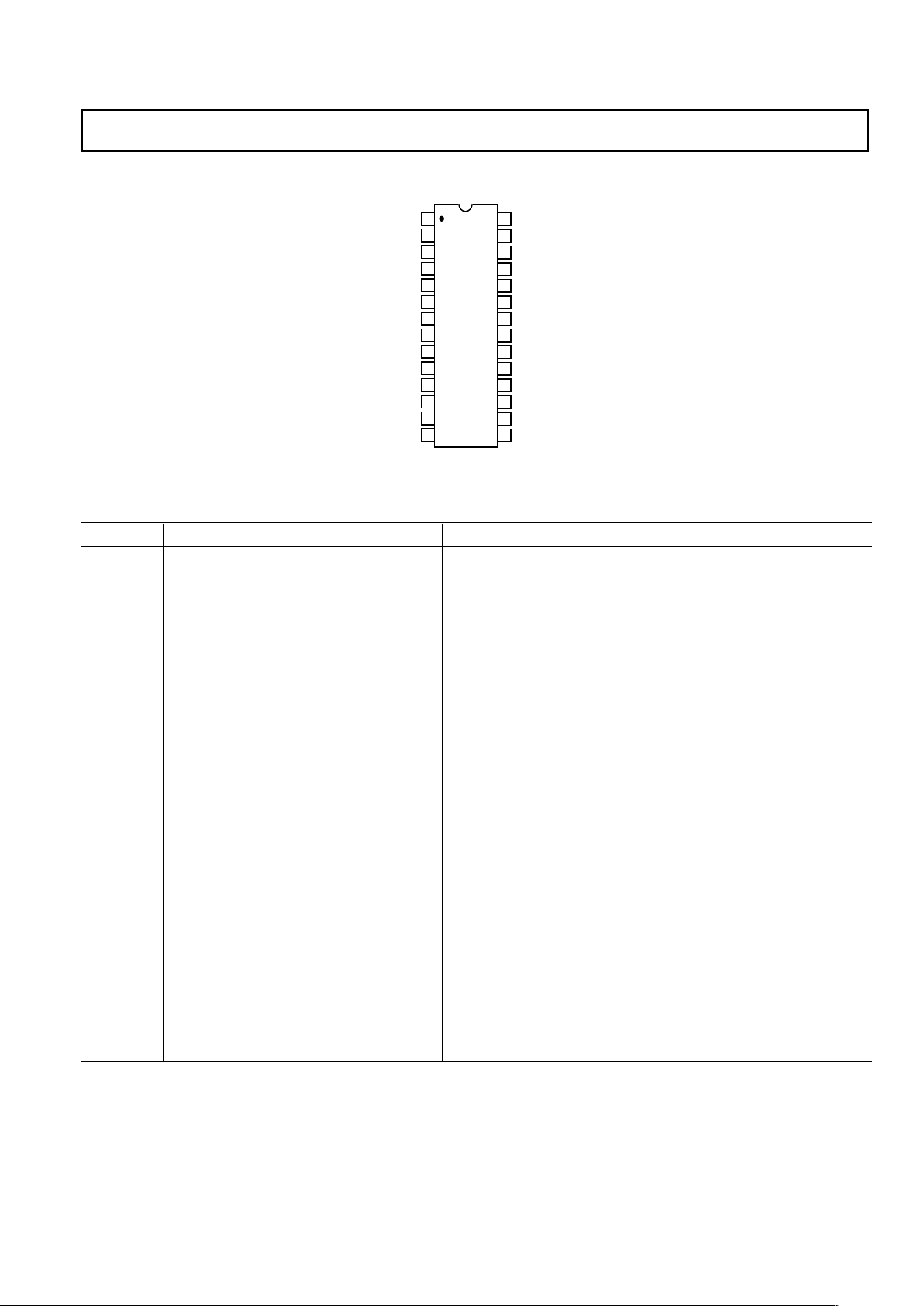
Pin No. Mnemonic Type Description
1 CDSCLK1 DI CDS Reference Level Sampling Clock
2 CDSCLK2 DI CDS Data Level Sampling Clock
3 ADCCLK DI A/D Converter Sampling Clock
4 OEB DI Output Enable, Active Low
5 DRVDD P Digital Output Driver Supply
6 DRVSS P Digital Output Driver Ground
7 D7 DO Data Output MSB. ADC DB15 High Byte, ADC DB7 Low Byte
8 D6 DO Data Output. ADC DB14 High Byte, ADC DB6 Low Byte
9 D5 DO Data Output. ADC DB13 High Byte, ADC DB5 Low Byte
10 D4 DO Data Output. ADC DB12 High Byte, ADC DB4 Low Byte
11 D3 DO Data Output. ADC DB11 High Byte, ADC DB3 Low Byte
12 D2 DO Data Output. ADC DB10 High Byte, ADC DB2 Low Byte
13 D1 DO Data Output. ADC DB9 High Byte, ADC DB1 Low Byte
14 D0 DO Data Output LSB. ADC DB8 High Byte, ADC DB0 Low Byte
15 SDATA DI/DO Serial Interface Data Input/Output
16 SCLK DI Serial Interface Clock Input
17 SLOAD DI Serial Interface Load Pulse
18, 28 AVDD P 5 V Analog Supply
19, 27 AVSS P Analog Ground
20 CAPB AO ADC Bottom Reference Voltage Decoupling
21 CAPT AO ADC Top Reference Voltage Decoupling
22 VINB AI Analog Input, Blue Channel
23 CML AO Internal Bias Level Decoupling
24 VING AI Analog Input, Green Channel
25 OFFSET AO Clamp Bias Level Decoupling
26 VINR AI Analog Input, Red Channel
TYPE: AI = Analog Input, AO = Analog Output, DI = Digital Input, DO = Digital Output, P = Power.
PIN CONFIGURATION
TOP VIEW
(Not to Scale)
28
27
26
25
24
23
22
21
20
19
18
17
16
15
1
2
3
4
5
6
7
8
9
10
11
12
13
14
AD9826
CDSCLK1
AVD D
CDSCLK2
AVSS
VINR
ADCCLK
OFFSET
OEB
VING
DRVDD
DRVSS
CML
(MSB) D7
VINB
D6
CAPT
D5
CAPB
D4
AVSS
D3
AVD D
SLOAD
D2
SCLK
D1
(LSB) D0
SDATA

AD9826
–6–
REV. A
DEFINITIONS OF SPECIFICATIONS
INTEGRAL NONLINEARITY (INL)
Integral nonlinearity error refers to the deviation of each individual
code from a line drawn from “zero scale” through “positive full
scale.” The point used as “zero scale” occurs 1/2 LSB before the
first code transition. “Positive full scale” is defined as a level
1 1/ 2 LSB beyond the last code transition. The deviation is
measured from the middle of each particular code to the true
straight line.
DIFFERENTIAL NONLINEARITY (DNL)
An ideal ADC exhibits code transitions that are exactly 1 LSB
apart. DNL is the deviation from this ideal value. Thus every
code must have a finite width. No missing codes guaranteed
to 16-bit resolution indicates that all 65536 codes, respectively, must be present over all operating ranges.
OFFSET ERROR
The first ADC code transition should occur at a level 1/2 LSB
above the nominal zero scale voltage. The offset error is the
deviation of the actual first code transition level from the
ideal level.
GAIN ERROR
The last code transition should occur for an analog value
1 1/2 LSB below the nominal full scale voltage. Gain error is
the deviation o f the actual difference between first and last
code transitions and the ideal difference between the first and
last code transitions.
INPUT REFERRED NOISE
The rms output noise is measured using histogram techniques.
The ADC output codes’ standard deviation is calculated in
LSB, and can be converted to an equivalent voltage, using the
relationship 1 LSB = 4 V/65536 = 61 µV. The noise may then
be referred to the input of the AD9826 by dividing by the
PGA gain.
CHANNEL-TO-CHANNEL CROSSTALK
In an ideal 3-channel system, the signal in one channel will not
influence the signal level of another channel. The channel-tochannel crosstalk specification is a measure of the change that
occurs in one channel as the other two channels are varied. In
the AD9826, one channel is grounded and the other two channels are exercised with full scale input signals. The change in the
output codes from the first channel is measured and compared
with the result when all three channels are grounded. The difference is the channel-to-channel crosstalk, stated in LSB.
APERTURE DELAY
The aperture delay is the time delay that occurs from when a
sampling edge is applied to the AD9826 until the actual sample
of the input signal is held. Both CDSCLK1 and CDSCLK2
sample the input signal during the transition from high to low,
so the aperture delay is measured from each clock’s falling edge
to the instant the actual internal sample is taken.
POWER SUPPLY REJECTION
Power supply rejection specifies the maximum full-scale change
that occurs from the initial value when the supplies are varied
over the specified limits.
 Loading...