ANALOG DEVICES AD9822 Service Manual
Complete 14-Bit
www.BDTIC.com/ADI
FEATURES
14-bit 15 MSPS ADC
No missing codes guaranteed
3-channel operation up to 15 MSPS
1-channel operation up to 12.5 MSPS
Correlated double sampling
1–6× programmable gain
±350 mV programmable offset
Input clamp circuitry
Internal voltage reference
Multiplexed byte-wide output (8 + 6 format)
3-wire serial digital interface
3 V/5 V digital I/O compatibility
28-Lead SOIC or SSOP
Low power CMOS: 385 mW (typ)
Power-down mode: <1 mW
APPLICATIONS
Flatbed document scanners
Film scanners
Digital color copiers
Multifunction peripherals
CCD/CIS Signal Processor
AD9822
GENERAL DESCRIPTION
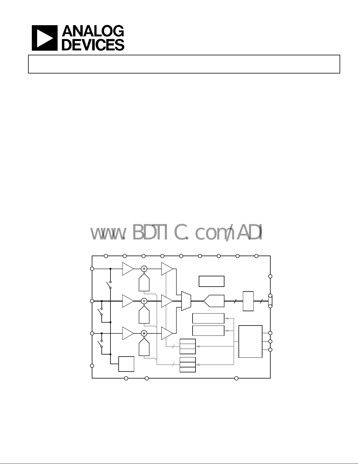
The AD9822 is a complete analog signal processor for CCD
imaging applications. It features a 3-channel architecture designed
to sample and condition the outputs of trilinear color CCD
arrays. Each channel consists of an input clamp, correlated double
sampler (CDS), offset DAC, and programmable gain amplifier
(PGA) multiplexed to a high performance 14-bit ADC.
The CDS amplifiers may be disabled for use with sensors such
as contact image sensors (CIS) and CMOS active pixel sensors,
which do not require CDS.
The 14-bit digital output is multiplexed into an 8-bit output
word that is accessed using two read cycles. The internal
registers are programmed through a 3-wire serial interface and
provide adjustment of the gain, offset, and operating mode.
The AD9822 operates from a single 5 V power supply,
consumes 385 mW of power typically, and is packaged in a
28-lead SOIC or SSOP.
FUNCTIONAL BLOCK DIAGRAM
DRVDD DRVSSAVDD AVSSCAPT CAPBAVDD AVSS CML
VINR
VING
VINB
OFFSET
CDS PGA
9-BIT
DAC
CDS
9-BIT
DAC
CDS
9-BIT
DAC
INPUT
CLAMP
BIAS
PGA
PGA
Rev. B
Information furnished by Analog Devices is believed to be accurate and reliable.
However, no responsibility is assumed by Analog Devices for its use, nor for any
infringements of patents or other rights of third parties that may result from its use.
Specifications subject to change without notice. No license is granted by implication
or otherwise under any patent or patent rights of Analog Devices. Trademarks and
registered trademarks are the property of their respective owners.
66
99
Figure 1.
AD9822
BAND GAP
REFERENCE
14 8
3:1
MUX
RED
GREEN
BLUE
RED
GREEN
BLUE
14-BIT
ADC
CONFIGURATION
REGISTER
MUX
REGISTER
GAIN
REGISTERS
OFFSET
REGISTERS
One Technology Way, P.O. Box 9106, Norwood, MA 02062-9106, U.S.A.
Tel: 781.329.4700 www.analog.com
Fax: 781.326.8703
14:8
MUX
DIGITAL
CONTROL
INTERFACE
ADCCLKCDSCLK2CDSCLK1
© 2005 Analog Devices, Inc. All rights reserved.
OEB
DOUT
SCLK
SLOAD
SDATA
00623-001

AD9822
www.BDTIC.com/ADI
TABLE OF CONTENTS
Specifications..................................................................................... 3
1-Channel CDS Mode ............................................................... 12
Analog Specifications................................................................... 3
Digital Specifications ................................................................... 4
Timing Specifications .................................................................. 5
Absolute Maximum Ratings............................................................ 6
Thermal Characteristics .............................................................. 6
ESD Caution.................................................................................. 6
Pin Configuration and Function Descriptions............................. 7
Te r m in o l o g y ...................................................................................... 8
Functional Description ..................................................................12
3-Channel CDS Mode................................................................ 12
3-Channel SHA Mode................................................................ 12
REVISION HISTORY
2/05—Rev. A to Rev. B
Changes to Format ............................................................. Universal
Changes to Ordering Guide.......................................................... 18
Updated Outline Dimensions....................................................... 18
1-Channel SHA Mode ............................................................... 12
Internal Register Descriptions .................................................. 13
Circuit Operation ........................................................................... 15
Analog Inputs—CDS Mode...................................................... 15
External Input Coupling Capacitors........................................ 15
Analog Inputs—SHA Mode...................................................... 16
Programmable Gain AmplifierS (PGA) .................................. 16
Applications..................................................................................... 17
Circuit and Layout Recommendations ................................... 17
Outline Dimensions....................................................................... 18
Ordering Guide .......................................................................... 18
12/99—Rev. 0 to Rev. A
Rev. B | Page 2 of 20
AD9822
www.BDTIC.com/ADI
SPECIFICATIONS
ANALOG SPECIFICATIONS
T
to T
MIN
Table 1.
Parameter Min Typ Max Unit
MAXIMUM CONVERSION RATE
3-Channel Mode with CDS 15 MSPS
1-Channel Mode with CDS 12.5 MSPS
ACCURACY (ENTIRE SIGNAL PATH)
ADC Resolution 14 Bits
Integral Nonlinearity (INL) −17.0/+3.5 LSB
Differential Nonlinearity (DNL) −0.65/+0.75 LSB
No Missing Codes 14 Bits
Offset Error −240 −19 +200 mV
Gain Error −1.4 +3.5 +6.9 % FSR
ANALOG INPUTS
Input Signal Range
Allowable Reset Transient1 1.0 V
Input Limits
Input Capacitance 10 pF
Input Bias Current 10 nA
AMPLIFIERS
PGA Gain at Minimum 1 V/V
PGA Gain at Maximum 5.7 V/V
PGA Gain Resolution2 64 Steps
PGA Gain Monotonicity Guaranteed
Programmable Offset at Minimum −350 mV
Programmable Offset at Maximum +350 mV
Programmable Offset Resolution 512 Steps
Programmable Offset Monotonicity Guaranteed
NOISE AND CROSSTALK
Total Output Noise @ PGA Minimum 1.5 LSB rms
Total Output Noise @ PGA Maximum 6.0 LSB rms
Channel-to-Channel Crosstalk @ 6 MHz <1 LSB
POWER SUPPLY REJECTION
AVDD = 5 V ± 0.25 V 0.063 0.9 % FSR
DIFFERENTIAL VREF (@ 25°C)
CAPT to CAPB (2 V ADC Full-Scale Range) 0.94 1.0 1.06 V
TEMPERATURE RANGE
Operating 0 +70 °C
Storage −65 +150 °C
POWER SUPPLIES
AVDD 4.75 5.0 5.25 V
DRVDD 3.0 5.0 5.25 V
OPERATING CURRENT
AVDD 73 mA
DRVDD 4 mA
Power-Down Mode Current 150 µA
, AVDD = 5 V, DRVDD = 5 V, CDS mode, f
MAX
INL @ 6 MHz −10.5/+1.5 LSB
DNL @ 6 MHz −1.0 −0.6/+0.65 +1.1 LSB
No Missing Codes @ 6 MHz 14 Bits
1
2
ADCCLK
= 15 MHz, f
2.0 V p-p
AVSS − 0.3 AVDD + 0.3 V
CDSCLK1
= f
= 5 MHz, PGA gain = 1, unless otherwise noted.
CDSCLK2
Rev. B | Page 3 of 20
AD9822
[
www.BDTIC.com/ADI
Parameter Min Typ Max Unit
POWER DISSIPATION
3-Channel Mode 385 450 mW
3-Channel Mode @ 6 MHz 335 410 mW
1-Channel Mode 300 mW
1-Channel Mode @ 6 MHz 250 mW
1
Linear input signal range is from 2 V to 4 V when the CCD’s reference level is clamped to 4 V by the AD9822’s input clamp.
1V TYP
RESET TRANSIENT
2
The PGA gain is approximately linear-in-dB and follows the equation:
4V SET BY INPUT CLAMP (3V OPTION ALSO AVAILABLE)
2V p-p MAX INPUT SIGNAL RANGE
7.5
Gain
=
⎡
+
7.41
⎢
⎣
]
where G is the register value. See Figure . 15
−
63
G
⎤
⎥
63
⎦
00623-002
DIGITAL SPECIFICATIONS
T
to T
MIN
Table 2.
Parameter Symbol Min Typ Max Unit
LOGIC INPUTS
High Level Input Voltage V
Low Level Input Voltage V
High Level Input Current I
Low Level Input Current I
Input Capacitance C
LOGIC OUTPUTS
High Level Output Voltage V
Low Level Output Voltage V
High Level Output Current I
Low Level Output Current I
, AVDD = 5 V, DRVDD = 5 V, CDS mode, f
MAX
ADCCLK
= 15 MHz, f
IH
IL
IH
IL
IN
OH
OL
OH
OL
CDSCLK1
= f
= 5 MHz, CL = 10 pF, unless otherwise noted.
CDSCLK2
2.0 V
0.8 V
10 µA
10 µA
10 pF
4.5 V
0.1 V
50 µA
50 µA
Rev. B | Page 4 of 20
AD9822
www.BDTIC.com/ADI
TIMING SPECIFICATIONS
T
to T
MIN
Table 3.
Parameter Symbol Min Typ Max Unit
CLOCK PARAMETERS
3-Channel Pixel Rate t
1-Channel Pixel Rate t
ADCCLK Pulse Width t
CDSCLK1 Pulse Width t
CDSCLK2 Pulse Width t
CDSCLK1 Falling to CDSCLK2 Rising t
ADCCLK Falling to CDSCLK2 Rising t
CDSCLK2 Rising to ADCCLK Rising t
CDSCLK2 Falling to ADCCLK Falling t
CDSCLK2 Falling to CDSCLK1 Rising t
ADCCLK Falling to CDSCLK1 Rising t
Aperture Delay for CDS Clocks t
SERIAL INTERFACE
Maximum SCLK Frequency f
SLOAD to SCLK Setup Time t
SCLK to SLOAD Hold Time t
SDATA to SCLK Rising Setup Time t
SCLK Rising to SDATA Hold Time t
SCLK Falling to SDATA Valid t
DATA OUTPUT
Output Delay t
Three-State to Data Valid t
Output Enable High to Three-State t
Latency (Pipeline Delay) 3 (Fixed) Cycles
, AVDD = 5 V, DRVDD = 5 V.
MAX
PRA
PRB
ADCLK
C1
C2
C1C2
ADC2
C2ADR
C2ADF
C2C1
ADC1
AD
SCLK
LS
LH
DS
DH
RDV
OD
DV
HZ
67 ns
80 ns
30 ns
10 ns
10 ns
0 ns
0 ns
0 ns
30 40 ns
30 40 ns
0 ns
2 ns
10 MHz
10 ns
10 ns
10 ns
10 ns
10 ns
8 ns
10 ns
10 ns
Rev. B | Page 5 of 20
AD9822
www.BDTIC.com/ADI
ABSOLUTE MAXIMUM RATINGS
Table 4.
With
Respect
Parameter
VIN, CAPT, CAPB AVSS −0.3 AVDD + 0.3 V
Digital Inputs AVSS −0.3 AVDD + 0.3 V
AVDD AVSS −0.5 +6.5 V
DRVDD DRVSS −0.5 +6.5 V
AVSS DRVSS −0.3 +0.3 V
Digital Outputs DRVSS −0.3 DRVDD + 0.3 V
Junction Temperature 150 °C
Storage Temperature −65 +150 °C
Lead Temperature
(10 sec)
Stresses above those listed under Absolute Maximum Ratings
may cause permanent damage to the device. This is a stress
rating only; functional operation of the device at these or other
conditions above those indicated in the operational sections of
this specification is not implied. Exposure to absolute maximum
ratings for extended periods may affect device reliability.
To Min Max Unit
300 °C
THERMAL CHARACTERISTICS
28-Lead 300 Mil SOIC
= 71.4°C/W
θ
JA
θ
= 23°C/W
JC
28-Lead 5.3 mm SSOP
= 109°C/W
θ
JA
θ
= 39°C/W
JC
ESD CAUTION
ESD (electrostatic discharge) sensitive device. Electrostatic charges as high as 4000 V readily accumulate on
the human body and test equipment and can discharge without detection. Although this product features
proprietary ESD protection circuitry, permanent damage may occur on devices subjected to high energy
electrostatic discharges. Therefore, proper ESD precautions are recommended to avoid performance
degradation or loss of functionality.
Rev. B | Page 6 of 20
 Loading...