Complete 12-Bit 6 MSPS
a
FEATURES
12-Bit 6 MSPS A/D Converter
No Missing Codes Guaranteed
3-Channel or 1-Channel Operation
Correlated Double Sampling
8-Bit Programmable Gain
8-Bit Offset Adjustment
PGA Output Monitor
Input Clamp Circuitry
Internal Voltage Reference
3-Wire Serial Interface
+3.3 V/+5 V Digital Output Compatibility
44-Lead MQFP Package
Low Power CMOS: 420 mW Typ
AVDD AVSS
PRODUCT DESCRIPTION
The AD9816 is a complete analog signal processor for CCD
and CIS applications. Included is all the necessary circuitry to
perform three-channel conditioning and sampling for a variety
of imaging applications.
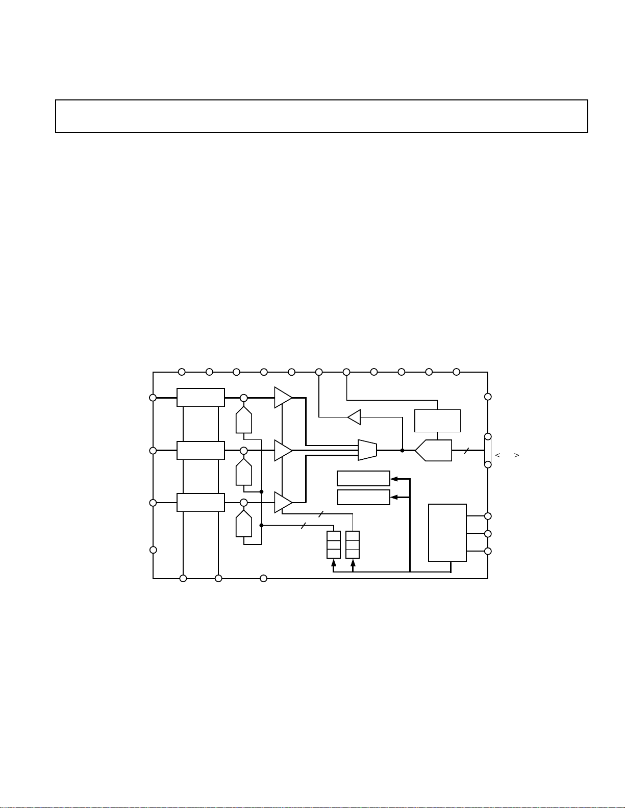
The signal chain consists of an input clamp, correlated double
sampler (CDS), offset adjust DAC, programmable gain amplifier and a 12-bit A/D converter. The CDS and input clamp may
be disabled for CIS applications.
The internal registers are programmed using a 3-wire serial
interface and provide adjustment of the gain, offset and operating mode.
The AD9816 operates from a +5 V supply, typically consumes
420 mW of power and is packaged in a 44-lead MQFP.
FUNCTIONAL BLOCK DIAGRAM
CAPT CAPB CML PGAOUT VREF
CCD/CIS Signal Processor
AD9816
DVDD DVSS DRVDD DRVSS
VINR
VING
VINB
OFFSET
CLAMP/CDS
CLAMP/CDS
CLAMP/CDS
CDSCLK1
6100mV
+
DAC
+
DAC
+
DAC
OFFSET
REGISTERS
CDSCLK2 ADCCLK
1X–6X
PGA
PGA
PGA
AD9816
OEB
BANDGAP
REFERENCE
ADC
DIGITAL
CONTROL
PORT
12
DOUT
11:0
SCLK
SLOAD
SDATA
MUX
MUX
REGISTER
CONFIGURATION
R
G
B
REGISTER
R
G
REGISTERS
B
GAIN
8
8
12-BIT
REV. A
Information furnished by Analog Devices is believed to be accurate and
reliable. However, no responsibility is assumed by Analog Devices for its
use, nor for any infringements of patents or other rights of third parties
which may result from its use. No license is granted by implication or
otherwise under any patent or patent rights of Analog Devices.
One Technology Way, P.O. Box 9106, Norwood, MA 02062-9106, U.S.A.
Tel: 781/329-4700 World Wide Web Site: http://www.analog.com
Fax: 781/326-8703 © Analog Devices, Inc., 1998

AD9816–SPECIFICATIONS
(T
to T
ANALOG SPECIFICATIONS
f
CDSCLK1
= 2 MHz, f
= 2 MHz, PGA Gain = 1, Input Range = 3 V p-p, Input Capacitor = 1200 pF, unless otherwise noted)
CDSCLK2
MIN
with AVDD = +5.0 V, DVDD = +5.0 V, DRVDD = +5.0 V, CDS Mode, f
MAX
Parameter AD9816 AD9816-80010 Units
MAXIMUM CONVERSION RATE
3-Channel Mode with CDS 6 6 MSPS min
1-Channel Mode with CDS 6 6 MSPS min
ACCURACY (Includes Entire Signal Path)
ADC Resolution 12 12 Bits min
Differential Nonlinearity (DNL) ±0.4 ±0.75 LSB typ
±1.0 LSB max
No Missing Codes 12 Bits Guaranteed
Integral Nonlinearity (INL) ±1.5 ±2.5 LSB typ
±4.0 LSB max
Offset Error 2.4 % FSR max
Gain Error
ANALOG INPUTS
Input Voltage Range
Input Limits
1
2
3
4.3 % FSR max
0 0 V min
3 3 V max
AVSS – 0.3 AVSS – 0.3 V min
AVDD + 0.3 AVDD + 0.3 V max
Input Capacitance 10 10 pF typ
Input Current 10 10 nA typ
AMPLIFIERS
PGA Gain Range 1 1 V/V min
5.98 5.98 V/V max
PGA Gain Resolution 256 256 Steps
Offset Range –100 –100 mV min
+100 +100 mV max
Offset Resolution 256 256 Steps
NOISE AND CROSSTALK
Total Output Noise at Min PGA Gain
Total Output Noise at Max PGA Gain
Channel-to-Channel Crosstalk
5
4
4
0.5 LSB rms typ
0.8 LSB rms typ
1LSB max
POWER SUPPLY REJECTION
(AVDD = +5 V/±0.25 V) 0.28 % FSR max
VOLTAGE REFERENCE
0.75 V Reference Tolerance (@ +25°C) ±20 mV max
1.5 V Reference Tolerance (@ +25°C) ±34 mV max
TEMPERATURE RANGE
Operating 0 0 °C min
+70 +70 °C max
POWER SUPPLIES
Operating Voltages
AVDD, DVDD +4.75 +4.75 V min
+5.25 +5.25 V max
DRVDD +3.3 +3.3 V min
+5.25 +5.25 V max
Operating Current 84 84 mA typ
POWER CONSUMPTION 420 420 mW typ
500 500 mW max
NOTES
1
Includes internal voltage reference error.
2
Input voltage range is the linear region over which the input signal can be processed by the input stage of the AD9816.
3
The input limits are defined as the maximum tolerable input voltage into the AD9816. This is not intended to be the linear input range of the device. Signals beyond
the input limits will turn on the overvoltage protection diodes.
4
The total output noise is measured with the inputs of the AD9816 grounded.
5
The channel-to-channel crosstalk is measured with one input grounded, and the other two inputs at full scale.
Specifications subject to change without notice.
ADCCLK
= 6 MHz,
–2–
REV. A

AD9816
(T
to T
DIGITAL SPECIFICATIONS
f
CDSCLK1
= 2 MHz, f
= 2 MHz, CL = 10 pF unless otherwise noted)
CDSCLK2
MIN
with AVDD = +5.0 V, DVDD = +5.0 V, DRVDD = +5.0 V, f
MAX
Parameter Symbol Min Typ Max Units
LOGIC INPUTS
High Level Input Voltage V
Low Level Input Voltage V
High Level Input Current I
Low Level Input Current I
Input Capacitance C
IH
IL
IH
IL
IN
3.5 V
10 µA
10 µA
10 pF
LOGIC OUTPUTS
High Level Output Voltage V
Low Level Output Voltage V
High Level Output Current I
Low Level Output Current I
Specifications subject to change without notice.
(T
TIMING SPECIFICATIONS
MIN
to T
OH
OL
OH
OL
with DVDD = +5.0 V, DRVDD = +5.0 V)
MAX
4.5 V
50 µA
50 µA
Parameter Symbol Min Typ Max Units
CLOCK PARAMETERS
3-Channel Conversion Rate t
1-Channel Conversion Rate t
ADCCLK Pulsewidth t
CDSCLK1 Pulsewidth t
CDSCLK2 Pulsewidth t
CDSCLK1 Falling to CDSCLK2 Rising t
ADCCLK Falling to CDSCLK2 Rising t
CDSCLK2 Falling to ADCCLK Falling t
CDSCLK2 Falling to CDSCLK1 Rising t
Aperture Delay for CDS Clocks t
CRA
CRB
ADCLK
C1
C2
C1C2
ADC2
C2AD
C2C1
AD
500 ns
160 ns
80 ns
20 ns
60 2 t
ADCLK
5ns
0ns
30 ns
10 ns
10 ns
SERIAL INTERFACE
Maximum SCLK Frequency f
SLOAD to SCLK Set-Up Time t
SCLK to SLOAD Hold Time t
SDATA to SCLK Rising Set-Up Time t
SCLK Rising to SDATA Hold Time t
SCLK Falling to SDATA Valid t
SCLK
LS
LH
DS
DH
RDV
10 MHz
10 ns
10 ns
10 ns
10 ns
10 ns
DATA OUTPUT
Output Delay t
3-State to Data Valid t
Output Enable High to 3-State t
OD
DV
HZ
13 ns
15 ns
5ns
Latency (Pipeline Delay) 3 (Fixed) ADCCLK Cycles
= 6 MHz,
ADCCLK
1.0 V
0.1 V
– 30 ns
–3–REV. A

AD9816
ANALOG
INPUTS
CDSCLK1
CDSCLK2
ADCCLK
OUTPUT
DATA
D11:D0
PGAOUT_T
PGAOUT_C
ANALOG
INPUTS
CDSCLK2
ADCCLK
OUTPUT
DATA
D11:D0
PGAOUT_T
PGAOUT_C
PIXEL n (R, G, B)
t
AD
t
C1
t
ADCLK
t
ADCLK
R(n–2) G(n–2) B(n–2) R(n–1) G(n–1) B(n–1) R(n) G(n) B(n) R(n+1)
G(n–1) B(n–1) R(n) G(n) B(n) R(n+1) G(n+1)
t
ADC2
t
C1C2
t
AD
t
C2C1
t
C2
t
C2AD
PIXEL (n+1) PIXEL (n+m)
t
CRA
t
OD
PIXEL (n+2)
B(n+1)
R(n+2)
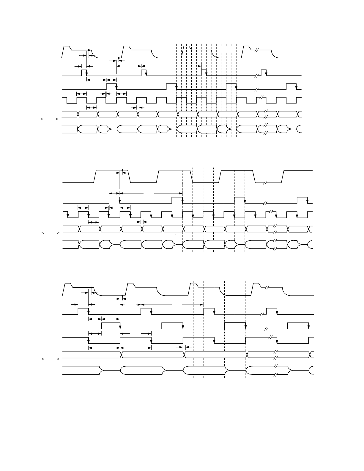
Figure 1. 3-Channel CDS Mode Timing
PIXEL n (R, G, B)
t
AD
t
C2
ADCLK
G(n–1)
t
ADC2
B(n–1)
t
ADCLK
t
R(n–2) G(n–2) B(n–2) R(n–1) G(n–1) B(n–1) R(n) G(n) B(n) R(n+1)
t
CRA
t
C2AD
t
OD
R(n) G(n) B(n) R(n+1) G(n+1)
PIXEL (n+2)PIXEL (n+1)
B(n+1)
R(n+2)
PIXEL (n+m)
ANALOG
INPUTS
CDSCLK1
CDSCLK2
ADCCLK
OUTPUT
DATA
D11:D0
PGAOUT_T
PGAOUT_C
Figure 2. 3-Channel SHA Mode Timing
t
AD
t
C1
t
C1C2
t
ADC2
PIXEL (n–4) PIXEL (n–3) PIXEL (n–2) PIXEL (n–1)
PIXEL (n–1) PIXEL n PIXEL (n+1)
PIXEL n PIXEL (n+m)
t
t
ADCLK
AD
t
C2C1
t
C2
t
C2AD
t
ADCLK
PIXEL (n+1)
t
CRB
t
OD
Figure 3. 1-Channel CDS Mode Timing
PIXEL (n+2)
PIXEL (n+2)
–4–
REV. A

AD9816
ANALOG
INPUTS
CDSCLK2
ADCCLK
OUTPUT
DATA
,D11:D0.
PGAOUT_T
PGAOUT_C
ANALOG
INPUTS
CDSCLK1
CDSCLK2
PIXEL n PIXEL (n+m)
t
AD
t
C2
t
ADC2
t
PIXEL (n–4) PIXEL (n–3) PIXEL (n–2) PIXEL (n–1)
PIXEL (n–1) PIXEL n PIXEL (n+1) PIXEL (n+2)
ADCLK
t
C2AD
t
ADCLK
t
CRB
t
OD
PIXEL (n+2)PIXEL (n+1)
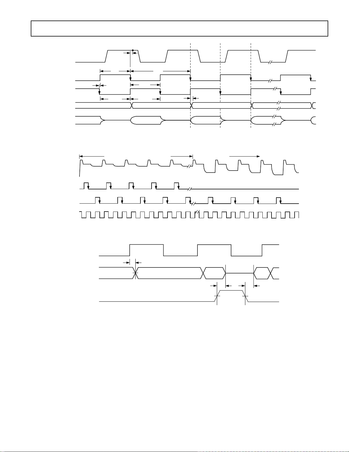
Figure 4. 1-Channel SHA Mode Timing
OPTICAL BLACK OR DUMMY PIXELS
EFFECTIVE PIXELS
ADCCLK
ADCCLK
OUTPUT
DATA
,D11:D0.
OEB
Figure 5. Line Clamp Timing for 3-Channel CDS Mode
t
OD
t
HZ
Figure 6. Output Enable Timing
t
DV
–5–REV. A
 Loading...