Analog Devices AD9806 Datasheet

Complete 10-Bit 18 MSPS
a
FEATURES
Pin-Compatible with Industry Standard AD9803
18 MSPS Correlated Double Sampler (CDS)
Low Noise PGA with 0 dB to 34 dB Gain Range
Low Noise Clamp Circuits
Analog Preblanking Function
10-Bit 18 MSPS A/D Converter
AUX Input with Input Clamp and PGA
Direct ADC Input with Input Clamp
AUXMID Input with PGA
3-Wire Serial Interface for Digital Control
Two Auxiliary 8-Bit DACs
3 V Single Supply Operation
Low Power: 65 mW @ 2.7 V Supply
48-Lead LQFP Package
APPLICATIONS
Camcorders (8 mm and DVC)
Digital Still Cameras
CCD Signal Processor
AD9806
PRODUCT DESCRIPTION
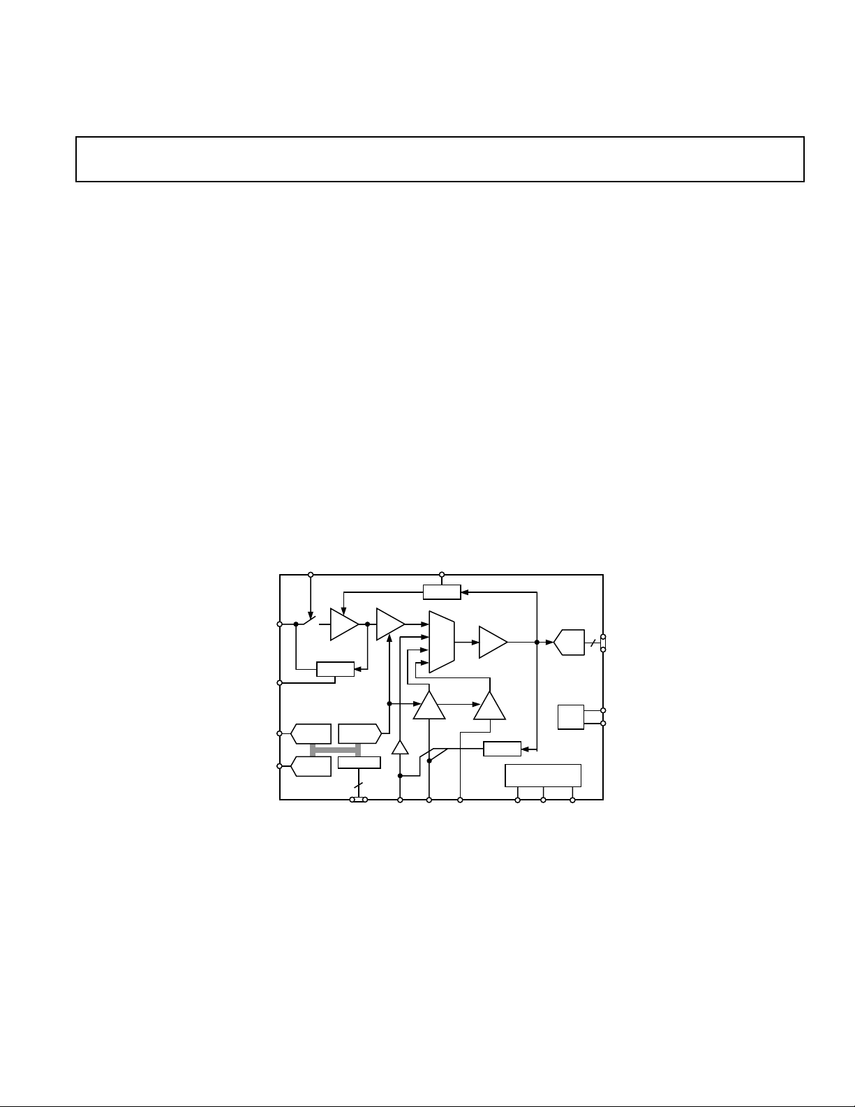
The AD9806 is a complete analog signal processor for CCD
applications. It features an 18 MHz single-channel architecture
designed to sample and condition the outputs of interlaced and
progressive scan area CCD arrays. The AD9806’s signal chain
consists of an input clamp, correlated double sampler (CDS),
digitally programmable gain amplifier (PGA), black level clamp,
and 10-bit A/D converter. Additional input modes are provided
for processing analog video signals.
The internal registers are programmed through a 3-wire serial
digital interface. Programmable features include gain adjustment, black level adjustment, input configuration, and powerdown modes.
The AD9806 operates from a single 3 V power supply, typically
dissipating 75 mW. Packaged in a space-saving 48-lead LQFP,
the AD9806 is specified over an operating temperature range of
–20°C to +85 C.
CCDIN
CLPDM
DAC1
DAC2
FUNCTIONAL BLOCK DIAGRAM
PBLK CLPOB
0dB~34dB
PGA
10-BIT
DAC
INTF
3
3-W INTF ADCIN AUXIN SHP SHD ADCCLK
8-BIT
DAC
8-BIT
DAC
CDS
CLAMP
CLAMP
MUX S/H
0dB
~
15dB
PGA
AUXMID
–4~14dB
PGA
CLAMP
AD9806
TIMING
GENERATOR
ADC
REF
10
DOUT
VRT
VRB
REV. 0
Information furnished by Analog Devices is believed to be accurate and
reliable. However, no responsibility is assumed by Analog Devices for its
use, nor for any infringements of patents or other rights of third parties
which may result from its use. No license is granted by implication or
otherwise under any patent or patent rights of Analog Devices.
One Technology Way, P.O. Box 9106, Norwood, MA 02062-9106, U.S.A.
Tel: 781/329-4700 World Wide Web Site: http://www.analog.com
Fax: 781/326-8703 © Analog Devices, Inc., 2001

AD9806–SPECIFICATIONS
(T
to T
GENERAL SPECIFICATIONS
MIN
, AVDD = DVDD = 3.0 V, f
MAX
Parameter Min Typ Max Unit
TEMPERATURE RANGE
Operating –20 +85 °C
Storage –65 +150 °C
POWER SUPPLY VOLTAGE
(For Functional Operation) 2.7 3.6 V
Analog, Digital, Digital Driver
POWER CONSUMPTION
(Selected through Serial Interface D-Reg)
Normal Operation (D-Reg 00) (Specified Under Each Mode of Operation)
High-Speed AUX Mode (D-Reg 01) (Specified Under AUX-Mode)
Reference Standby (D-Reg 10) 5 mW
Total Shut-Down Mode (D-Reg 11) 1 mW
MAXIMUM CLOCK RATE (Specified Under Each Mode of Operation) MHz
A/D CONVERTER
Resolution 10 Bits
Differential Nonlinearity (DNL) ± 0.5 ± 1.0 LSB
No Missing Codes GUARANTEED
Full-Scale Input Voltage 1.0 V
VOLTAGE REFERENCE
Reference Top Voltage (VRT) 2.0 V
Reference Bottom Voltage (VRB) 1.0 V
Specifications subject to change without notice.
= 18 MHz, unless otherwise noted.)
ADCCLK
DIGITAL SPECIFICATIONS
(DRVDD = 2.7 V, C
= 20 pF.)
L
Parameter Symbol Min Typ Max Unit
LOGIC INPUTS
High Level Input Voltage V
Low Level Input Voltage V
High Level Input Current I
Low Level Input Current I
Input Capacitance C
IH
IL
IH
IL
IN
2.1 V
0.6 V
10 µA
10 µA
10 pF
LOGIC OUTPUTS
High Level Output Voltage (I
= 2 mA) V
OH
Low Level Output Voltage (IOL = 2 mA) V
OH
OL
2.2 V
0.5 V
SERIAL INTERFACE TIMING (Figure 7)
Maximum SCLK Frequency 10 MHz
SDATA to SCLK Setup t
SCLK to SDATA Hold t
SLOAD to SCLK Setup t
SCLK to SLOAD Hold t
Specifications subject to change without notice.
DS
DH
LS
LH
10 ns
10 ns
10 ns
10 ns
–2–
REV. 0

AD9806
CCD-MODE SPECIFICATIONS
(T
to T
MIN
, AVDD = DVDD = 3.0 V, f
MAX
ADCCLK
= f
SHP
= f
= 18 MHz, unless otherwise noted.)
SHD
Parameter Min Typ Max Unit
POWER CONSUMPTION
VDD = 2.7 65 mW
V
= 3.0 75 mW
DD
VDD = 3.3 85 mW
MAXIMUM CLOCK RATE 18 MHz
CDS
Gain 0dB
Allowable CCD Reset Transient
Max Input Range before Saturation
1
1
1000 mV p-p
500 mV
PGA
Gain Control Resolution 10 Bits
Gain Range (See Figure 5a for Gain Curve)
Low Gain (Code 95)
Max Gain (1023)
2
2
–1 0 +1 dB
32 33 34 dB
BLACK LEVEL CLAMP
Clamp Level (Selected through Serial Interface E-Reg)
CLP0 (E-Reg 00) 32 LSB
CLP1 (E-Reg 01) 48 LSB
CLP2 (E-Reg 10) 64 LSB
CLP3 (E-Reg 11) 16 LSB
SIGNAL-TO-NOISE RATIO3 (@ Low PGA Gain) 74 dB
TIMING SPECIFICATIONS
Pipeline Delay 9 Cycles
Internal Clock Delay
Inhibited Clock Period (t
Output Delay (t
)14.516ns
OD
Output Hold Time (t
4
5
(tID)3ns
)10 ns
INHIBIT
)6 ns
HOLD
ADCCLK, SHP, SHD Clock Period 47 55.6 ns
ADCCLK High-Level/Low-Level 20 28 ns
SHP, SHD Minimum Pulsewidth 10 14 ns
SHP Rising Edge to SHD Rising Edge 20 28 ns
NOTES
1
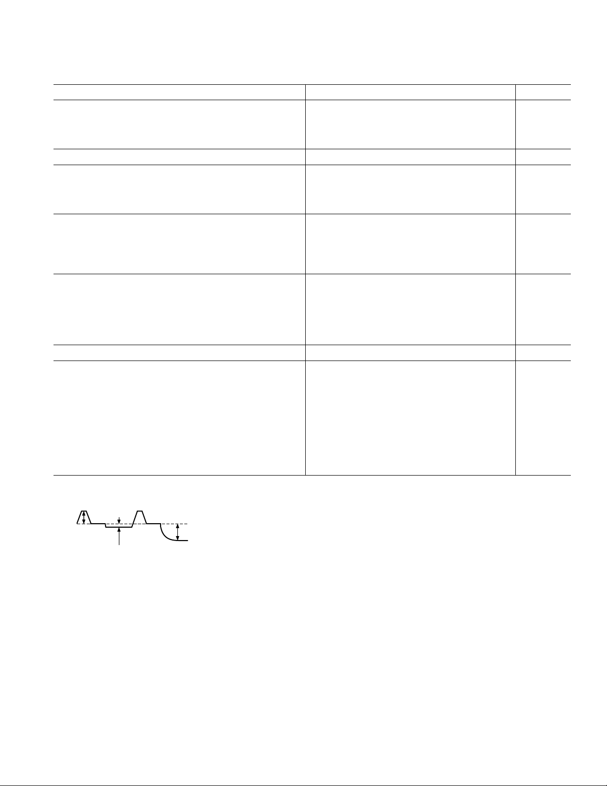
Input signal characteristics defined as follows:
500mV TYP
RESET
TRANSIENT
2
Use equations on page 8 to calculate gain.
3
SNR = 20 log10 (Full-Scale Voltage/RMS Output Noise).
4
20 pF loading; timing shown in Figure 1.
5
Internal aperture delay for actual sampling edge.
Specifications subject to change without notice.
200mV MAX
OPTICAL
BLACK PIXEL
1V MAX
INPUT
SIGNAL RANGE
REV. 0
–3–

AD9806–SPECIFICATIONS
(T
to T
AUX-MODE SPECIFICATIONS
MIN
, AVDD = DVDD = 3.0 V, f
MAX
Parameter Min Typ Max Unit
POWER CONSUMPTION
Normal (D-Reg 00) 50 mW
High-Speed (D-Reg 01) 95 mW
MAXIMUM CLOCK RATE
Normal (D-Reg 00) 18 MHz
High-Speed (D-Reg 01) 28.6 MHz
PGA (Gain Selected through Serial Interface F-Reg)
Max Input Range 700 mV p-p
Max Output Range 1000 mV p-p
Gain Control Resolution 7 Bits
Gain Range
Min Gain (Code 128) –2 dB
Max Gain (Code 255) 15 dB
ACTIVE CLAMP
Clamp Level (Selected through Serial Interface E-Reg)
CLP0 (E-Reg 00) 32 LSB
CLP1 (E-Reg 01) 48 LSB
CLP2 (E-Reg 10) 64 LSB
CLP3 (E-Reg 11) 16 LSB
TIMING SPECIFICATIONS
1
Pipeline Delay 9 Cycles
Internal Clock Delay (t
Output Delay (t
OD
Output Hold Time (t
NOTES
1
20 pF loading; timing shown in Figure 2.
Specifications subject to change without notice.
)
ID
) 14.5 16 ns
)7 ns
HOLD
= 18 MHz, unless otherwise noted.)
ADCCLK
AUXMID-MODE SPECIFICATIONS
MIN
, AVDD = DVDD = 3.0 V, f
MAX
= 18 MHz, unless otherwise noted.)
ADCCLK
(T
to T
Parameter Min Typ Max Unit
POWER CONSUMPTION 50 mW
MAXIMUM CLOCK RATE 18 MHz
PGA (Gain Selected through Serial Interface F-Reg)
Max Input Range 700 mV p-p
Max Output Range 1000 mV p-p
Gain Control Resolution 9 Bits
Gain Range (See Figure 5b for Gain Curve)
Min Gain (Code 512) –4 dB
Max Gain (Code 1023) 14 dB
MIDSCALE OFFSET LEVEL (AT MAX PGA GAIN) 462 512 562 LSB
TIMING SPECIFICATIONS
1
Pipeline Delay 9 Cycles
Internal Clock Delay (t
Output Delay (t
OD
Output Hold Time (t
NOTES
1
20 pF loading; timing shown in Figure 2.
Specifications subject to change without notice.
)
ID
) 14.5 16 ns
)7 ns
HOLD
–4–
REV. 0
 Loading...