Analog Devices AD9805 7 Datasheet
Complete 12-Bit/10-Bit 6 MSPS
a
FEATURES
Pin Compatible 12-Bit and 10-Bit Versions
12-Bit/10-Bit 6 MSPS A/D Converter
Integrated Triple Correlated Double Sampler
3-Channel, 2 MSPS Color Mode
13 – 43 Analog Programmable Gain Amplifier
Pixel-Rate Digital Gain Adjustment
Pixel-Rate Digital Offset Adjustment
Internal Voltage Reference
No Missing Codes Guaranteed
Microprocessor-Compatible Control Interface
+3.3 V/+5 V Digital I/O Compatibility
Low Power CMOS: 500 mW
64-Pin PQFP Surface Mount Package
PRODUCTION DESCRIPTION
The AD9807 and AD9805 are complete CCD/CIS imaging
decoders and signal processors on a single monolithic integrated
circuit. The input of the AD9807/AD9805 allows direct ac
coupling of the charge-coupled device (CCD) or contact image
sensor (CIS) output(s). The AD9807/AD9805 includes all the
circuitry to perform three-channel correlated double sampling
(CDS) and programmable gain adjustment of the CCD output;
a 12-bit or 10-bit analog-to-digital converter (ADC) quantizes
the analog signal. After digitization, the on-board digital signal
processor (DSP) circuitry allows pixel rate offset and gain correction. The DSP also corrects odd/even CCD register imbalance
errors. A parallel control bus provides a simple interface to
8-bit microcontrollers. The AD9807/AD9805 comes in a
space saving 64-pin plastic quad flatpack (PQFP) and is specified
over the commercial (0°C to +70°C) temperature range. By
disabling the CDS, the AD9807/AD9805 are also suitable for
non-CCD applications, or applications that do not require
CDS, such as CIS signal processing.
PRODUCT HIGHLIGHTS
The AD9807/AD9805 offers a complete, single chip CCD
imaging front end in a 64-pin plastic quad flatpack (PQFP).
On-Chip PGA—The AD9807/AD9805 includes a 3-channel
analog programmable gain amplifier; it is programmable from
1× to 4× in 16 increments.
CCD/CIS Signal Processors
AD9807/AD9805
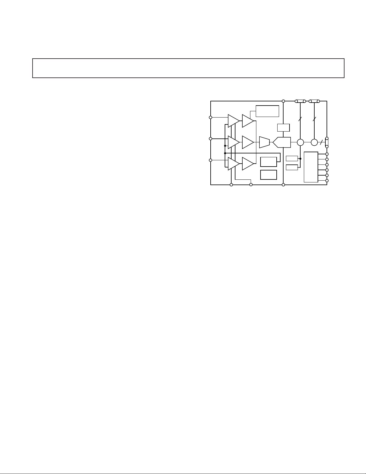
FUNCTIONAL BLOCK DIAGRAM
PIXEL
OFFSET
8-10 12-10
–
MPU
MPU
PORT
PORT
PIXEL
GAIN
X
12-10
DOUT
CSB
RD
WR
A2
A1
A0
VREF
AD9807/AD9805
RED
VINR
GREEN
VING
BLUE
VINB
PGA
CDS
PGA
PGA
CDS
PGA
PGA
CDS
CDSCLK1 CDSCLK2 ADCCLK
GAIN
GAIN
REGISTERS
REGISTERS
MUX ADC
MUX
INPUT
INPUT
OFFSET
OFFSET
CONFIG
CONFIG
REGS
REGS
REF
REF
ODD
ODD
EVEN
EVEN
On-Chip CDS—An integrated 3-channel correlated double
sampler allows easy ac coupling directly from the CCD sensor
outputs. Additionally, the CDS reduces low frequency noise
and reset feedthrough.
On-Chip Voltage Reference—The AD9807/AD9805 includes a
2 V bandgap reference that allows the input range of the device to
be configured for input spans up to 4 V.
6 MSPS A/D Converter—A highly linear 12-bit or 10-bit A/D
converter sequentially digitizes the red, green and blue CDS
outputs ensuring no missing code performance. The user may also
configure the AD9807/AD9805 for single channel operation.
Digital Gain & Offset Correction—Pixel rate digital gain and
offset correction blocks allow precise repeatable correction of
imaging system error sources.
Digital I/O Compatibility—The AD9807/AD9805 offers
+3.3 V/+5 V logic level compatibility.
Pin-Compatible 12-Bit and 10-Bit Versions—The AD9807 is
also offered in a pin-compatible 10-bit version, the AD9805,
allowing upgrade-ability and simplifying design issues across
different scanner models.
REV. 0
Information furnished by Analog Devices is believed to be accurate and
reliable. However, no responsibility is assumed by Analog Devices for its
use, nor for any infringements of patents or other rights of third parties
which may result from its use. No license is granted by implication or
otherwise under any patent or patent rights of Analog Devices.
One Technology Way, P.O. Box 9106, Norwood, MA 02062-9106, U.S.A.
Tel: 617/329-4700 World Wide Web Site: http://www.analog.com
Fax: 617/326-8703 © Analog Devices, Inc., 1997

AD9807–SPECIFICA TIONS
(T
to T
with AVDD = +5.0 V, DVDD = +5.0 V, f
MAX
ANALOG SPECIFICATIONS
MIN
PGA Gain = 1 unless otherwise noted)
Parameter Min Typ Max Units
RESOLUTION 12 Bits
CONVERSION RATE
3-Channel Mode With CDS 6 MSPS
1-Channel Mode With CDS
DC ACCURACY
Integral Nonlinearity (INL)
Differential Nonlinearity (DNL)
1
2
2
6 MSPS
1.5 LSB
0.4 0.75 LSB
No Missing Codes 12 Bits Guaranteed
Unipolar Offset Error (@ +25°C) 0.4 % FSR
Gain Error (@ +25°C) 1.2 % FSR
ANALOG INPUTS
Full-Scale Input Span 0.0625 4 V p-p
Input Limits
3
AVSS – 0.3 V AVDD + 0.3 V
Input Capacitance 10 pF
Input Bias Current 0.01 µA
Input Referred Noise 0.3 LSB rms
PSRR (AVDD = +5 V ± 0.25 V) 0.06 % FSR
INTERNAL VOLTAGE REFERENCE
1 V Output Tolerance (@+25°C) ±15 mV
2 V Output Tolerance (@+25°C) ±30 mV
POWER SUPPLIES
Operating Voltages
AV
DV
DD
DD
+4.75 +5.25 V
+4.75 +5.25 V
Operating Current
AV
DV
DD
DD
73 86 mA
16.6 20 mA
POWER CONSUMPTION 450 530 mW
TEMPERATURE RANGE
Operating 0 +70 °C
NOTES
1
Blue and green channels. Red channel conversion rate for 1-channel mode is 5 MSPS.
2
Measured with 4 V p-p input range.
3
Input signals exceeding these limits are subject to excessive overvoltage recovery times.
Specifications subject to change without notice.
ADCCLK
= 6 MSPS, f
CDSCLK1
= 2 MSPS, f
CDSCLK2
= 2 MSPS,
(T
to T
DIGITAL SPECIFICATIONS
MIN
with AVDD = +5.0 V, DVDD = +5.0 V, f
MAX
CL = 20 pF, unless otherwise noted)
ADCCLK
= 6 MSPS, f
CDSCLK1
= 2 MSPS, f
CDSCLK2
= 2 MSPS,
Parameter Symbol Min Typ Max Units
LOGIC INPUTS
High Level Input Voltage V
Low Level Input Voltage V
High Level Input Current I
Low Level Input Current I
Input Capacitance C
IH
IL
IH
IL
IN
2.0 V
0.8 V
10 µA
10 µA
10 pF
LOGIC OUTPUTS
High Level Output Voltage (I
High Level Output Voltage (I
Low Level Output Voltage (I
Low Level Output Voltage (I
Output Capacitance C
Specifications subject to change without notice.
= 50 µA) V
OH
= 0.5 mA) V
OH
= 50 µA) V
OL
= –0.6 mA) V
OL
OH
OH
OL
OL
OUT
–2–
4.5 4.9 V
2.4 V
0.1 V
0.4 V
5pF
REV. 0

AD9805–SPECIFICA TIONS
(T
to T
MIN
MAX
ANALOG SPECIFICATIONS
PGA Gain = 1 unless otherwise noted)
with AVDD = +5.0 V, DVDD = +5.0 V, f
ADCCLK
= 6 MSPS, f
CDSCLK1
AD9807/AD9805
= 2 MSPS, f
CDSCLK2
= 2 MSPS,
Parameter Min Typ Max Units
RESOLUTION 10 Bits
CONVERSION RATE
3-Channel Mode With CDS 6 MSPS
1-Channel Mode With CDS
DC ACCURACY
Integral Nonlinearity (INL)
Differential Nonlinearity (DNL)
1
2
2
6 MSPS
1.0 LSB
0.5 LSB
No Missing Codes 10 Bits Guaranteed
Unipolar Offset Error (@ +25°C) 0.6 % FSR
Gain Error (@ +25°C) 1.2 % FSR
ANALOG INPUTS
Full-Scale Input Span 0.0625 4 V p-p
Input Limits
3
AVSS – 0.3 V AVDD + 0.3 V
Input Capacitance 10 pF
Input Bias Current 0.01 µA
Input Referred Noise 0.1 LSB rms
PSRR (AVDD = +5 V ± 0.25 V) 0.06 % FSR
INTERNAL VOLTAGE REFERENCE
1 V Output Tolerance (@ +25°C) ±15 mV
2 V Output Tolerance (@ +25°C) ±30 mV
POWER SUPPLIES
Operating Voltages
AV
DV
DD
DD
+4.75 +5.25 V
+4.75 +5.25 V
Operating Current
AV
DV
DD
DD
73 86 mA
16.6 20 mA
POWER CONSUMPTION 450 530 mW
TEMPERATURE RANGE
Operating 0 +70 °C
NOTES
1
Blue and green channels. Red channel conversion rate for 1-channel mode is 5 MSPS.
2
Measured with 4 V p-p input range.
3
Input signals exceeding these limits are subject to excessive overvoltage recovery times.
Specifications subject to change without notice.
(T
to T
DIGITAL SPECIFICATIONS
MIN
with AVDD = +5.0 V, DVDD = +5.0 V, f
MAX
CL = 20 pF, unless otherwise noted)
ADCCLK
= 6 MSPS, f
CDSCLK1
= 2 MSPS, f
CDSCLK2
= 2 MSPS,
Parameter Symbol Min Typ Max Units
LOGIC INPUTS
High Level Input Voltage V
Low Level Input Voltage V
High Level Input Current I
Low Level Input Current I
Input Capacitance C
IH
IL
IH
IL
IN
2.0 V
0.8 V
10 µA
10 µA
10 pF
LOGIC OUTPUTS
High Level Output Voltage (I
High Level Output Voltage (I
Low Level Output Voltage (I
Low Level Output Voltage (I
Output Capacitance C
Specifications subject to change without notice.
REV. 0
= 50 µA) V
OH
= 0.5 mA) V
OH
= 50 µA) V
OL
= –0.6 mA) V
OL
OH
OH
OL
OL
OUT
4.5 4.9 V
2.4 V
0.1 V
0.4 V
5pF
–3–
AD9807/AD9805
(T
to T
TIMING SPECIFICATIONS
MIN
Parameter Symbol Min Typ Max Units
CLOCK PARAMETERS
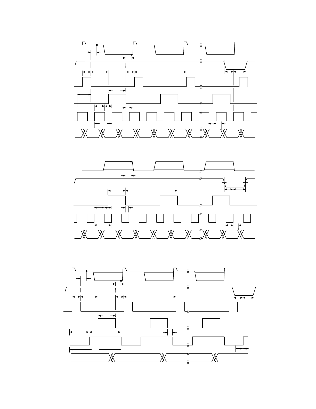
3-Channel Conversion Rate t
1-Channel Conversion Rate t
CDSCK1 Pulse Width t
CDSCK1 Pulse Width t
CDSCK2 Pulse Width t
CDSCK2 Pulse Width t
CDS Clocks Digital Quiet Time t
CDSCK2 Falling to CDSCK1 Rising t
CDSCK2 Falling to CDSCK1 Rising t
CDSCK1 Falling to CDSCK2 Rising t
CDSCK1 Falling to CDSCK2 Rising t
ADCCLK Rising to CDSCK1 Falling t
ADCCLK Pulse Width t
ADCCLK Period t
ADCCLK Period (Red Single Channel Mode) t
3-Channel Settling Time t
1-Channel Settling Time (B and G Only) t
ADCCLK Rising to Control Data Setup t
ADCCLK Rising to Control Data Hold t
STRTLN Rising, Falling Setup t
STRTLN Rising, Falling Hold t
Aperture Delay t
REGISTER WRITE/READ
Address Setup Time t
Address Hold Time t
Data Setup Time t
Data Hold Time t
Chip Select Setup Time t
Chip Select Hold Time t
Write Pulse Width t
Read Pulse Width t
Read To Data Valid t
DATA OUTPUT
Output Delay t
3-State to Data Valid t
Output Enable High to 3-State t
Latency 6 ADCCLK Cycles
with AVDD = +5.0 V, DVDD = +5.0 V, unless otherwise noted)
MAX
CRA
CRB
C1A
C1B
C2A
C2B
Q
C2C1A
C2C1B
C1C2A
C1C2B
C1AD
ACLK
CP
CP2
STL1
STL2
GOS
GOH
S
H
AD
AS
AH
DS
DH
CSS
CSH
PWW
PWR
DD
OD
EDV
HZ
500 ns
166 ns
30 ns
30 ns
30 ns
30 ns
20 ns
80 ns
40 ns
20 ns
20 ns
35 ns
50 ns
166 ns
200 ns
60 ns
30 ns
15 ns
15 ns
15 ns
15 ns
10 ns
15 ns
15 ns
15 ns
15 ns
15 ns
15 ns
25 ns
50 ns
40 ns
15 ns
15 ns
5ns
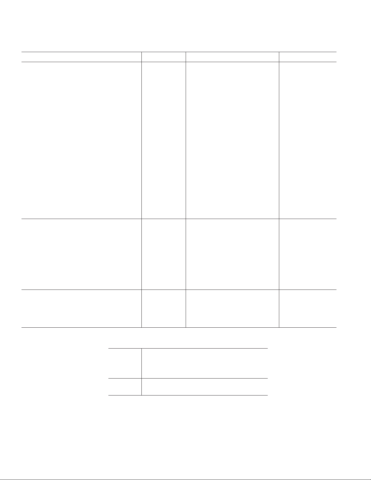
Table I. Output Controls
CSB 00000011
RDB 001111xx
WRB 010011xx
OEB xx010101
DOUT XQXDXZQZ
MPU MPU ADC
LEGEND:
x = Don't Care
X = Unknown (Not Recommended)
Q = Outputs
D = Inputs
Z = 3-State
–4–
REV. 0
AVDD
AVSS
CAPT
CAPT
CAPB
CAPB
VREF
CML
VINR
AVSS
VING
AVSS
VINB
AVSS
AVDD
STRTLN
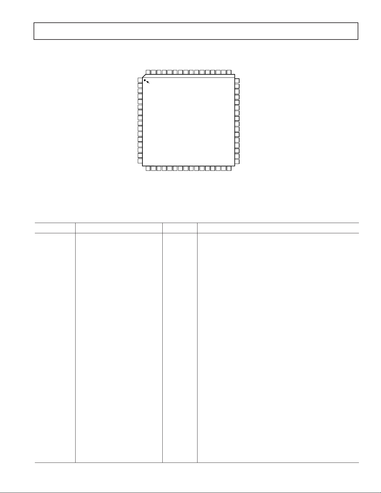
PIN CONFIGURATION
GAIN<8>
GAIN<6>
GAIN<7>
GAIN<5>
AD9807
TOP VIEW
(Not to Scale)
OFFSET<5>
OFFSET<6>
OFFSET<4>
GAIN<4>
GAIN<3>
GAIN<2>
OFFSET<2>
OFFSET<3>
OFFSET<1>
GAIN<0>
GAIN<1>
DVSS
OFFSET<0>
GAIN<9>
GAIN<10>
GAIN<11>
64 63 62 61 60 55 54 53 52 51 50 4959 58 57 56
1
PIN 1
2
IDENTIFIER
3
4
5
6
7
8
9
10
11
12
13
14
15
16
17 18 19 20 21 22 23 24 25 26 27 28 29 30 31 32
ADCCLK
CDSCLK1
CDSCLK2
OFFSET<7>
DVSS
DVDD
A2
DVDD
CSB
RDB
A1
48
A0
DOUT<11>
47
DOUT<10>
46
DOUT<9>
45
DOUT<8>
44
DOUT<7>/MPU<7>
43
DOUT<6>/MPU<6>
42
DRVDD
41
40
DRVSS
DOUT<5>/MPU<5>
39
38
DOUT<4>/MPU<4>
37
DOUT<3>/MPU<3>
36
DOUT<2>/MPU<2>
DOUT<1>/MPU<1>
35
34
DOUT<0>/MPU<0>
OEB
33
WRB
AD9807/AD9805
PIN DESCRIPTIONS
Pin No. Pin Name Type Description
1, 15 AVDD P +5 V Analog Supply.
2, 10, 12, 14 AVSS P Analog Ground.
3, 4 CAPT AO Reference Decoupling. See Figure 22.
5, 6 CAPB AO Reference Decoupling.
7 VREF AO Internal Reference Output. Decouple with 10 µF + 0.1 µF.
8 CML AO Internal Bias Voltage. Decouple with 0.1 µF.
9 VINR AI Analog Input, Red.
11 VING AI Analog Input, Green.
13 VINB AI Analog Input, Blue.
16 STRTLN DI STRTLN. Indicates beginning of scan line.
17 CDSCLK1 DI CDS Reset Clock Pulse Input.
18 CDSCLK2 DI CDS Data Clock Pulse Input.
19 ADCCLK DI A/D Sample Clock Input.
28, 52 DVSS P Digital Ground.
29, 51 DVDD P +5 V Digital Supply.
20 OFFSET<7> DI Pixel Rate Offset Coefficient Inputs. Most Significant Bit.
21–26 OFFSET<6:1> DI Pixel Rate Offset Coefficient Inputs.
27 OFFSET<0> DI Pixel Rate Offset Coefficient Inputs. Least Significant Bit.
30 CSB DI Chip Select. Active Low.
31 RDB DI Read Strobe. Active Low.
32 WRB DI Write Strobe. Active Low.
33 OEB DI Output Enable. Active Low.
34 DOUT<0>/MPU<0> DIO Data Output LSB/Register Input LSB
35–39, 42 DOUT<1:6>/MPU<1:6> DIO Data Outputs/Register Inputs.
40 DRVSS P Digital Driver Ground
41 DRVDD P Digital Driver Supply
43 DOUT<7>/MPU<7> DIO Data Output/Register Input MSB.
44–46 DOUT<8:10> DO Data Outputs.
47 DOUT<11> DO Data Output MSB.
48, 49, 50 A0, A1, A2 DI Register Select Pins.
53 GAIN<0> DI Pixel Rate Gain Coefficient Input. LSB.
54–63 GAIN<1:10> DI Pixel Rate Gain Coefficient Inputs.
64 GAIN<11> DI Pixel Rate Gain Coefficient Input. MSB.
TYPE: AI = Analog Input; AO = Analog Output; DI = Digital Input; DO = Digital Output; DIO = Digital Input/Output; P = Power.
REV. 0
–5–
AD9807/AD9805
AVDD
AVSS
CAPT
CAPT
CAPB
CAPB
VREF
CML
VINR
AVSS
VING
AVSS
VINB
AVSS
AVDD
STRTLN
NC = NO CONNECT
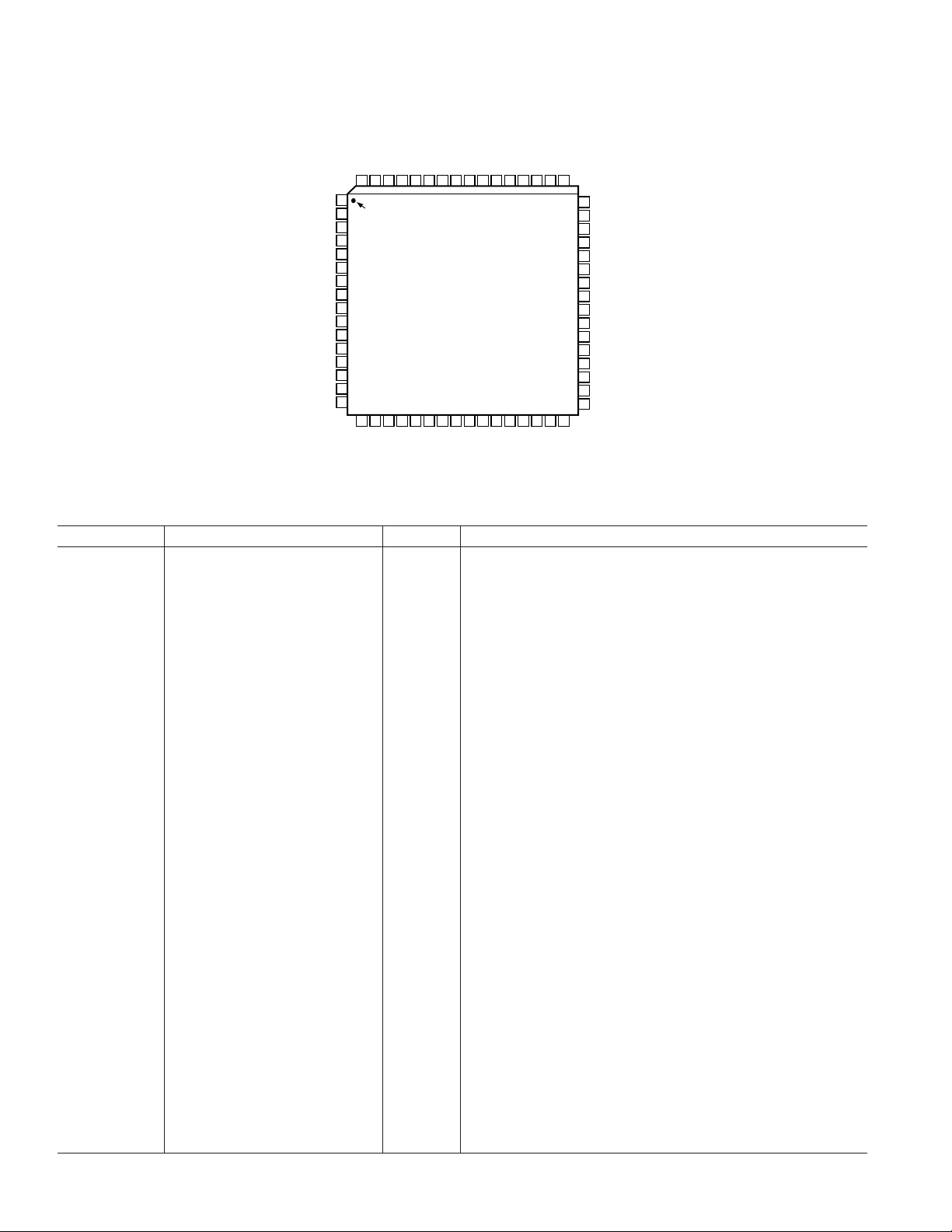
PIN CONFIGURATION
GAIN<8>
GAIN<6>
GAIN<7>
ADCCLK
OFFSET<7>
GAIN<4>
GAIN<5>
GAIN<3>
AD9805
TOP VIEW
(Not to Scale)
OFFSET<5>
OFFSET<6>
OFFSET<4>
GAIN<2>
GAIN<0>
GAIN<1>
OFFSET<2>
OFFSET<3>
OFFSET<1>
NC
DVSS
OFFSET<0>
GAIN<9>
64 63 62 61 60 55 54 53 52 51 50 4959 58 57 56
1
PIN 1
2
IDENTIFIER
3
4
5
6
7
8
9
10
11
12
13
14
15
16
17 18 19 20 21 22 23 24 25 26 27 28 29 30 31 32
CDSCLK1
CDSCLK2
PIN DESCRIPTIONS
NC
DVSS
DVDD
A2
DVDD
CSB
RDB
A1
48
A0
DOUT<9>
47
DOUT<8>
46
DOUT<7>
45
DOUT<6>
44
DOUT<5>/MPU<7>
43
DOUT<4>/MPU<6>
42
DRVDD
41
40
DRVSS
DOUT<3>/MPU<5>
39
38
DOUT<2>/MPU<4>
37
DOUT<1>/MPU<3>
36
DOUT<0>/MPU<2>
MPU<1>
35
34
MPU<0>
OEB
33
WRB
Pin No. Pin Name Type Description
1, 15 AVDD P +5 V Analog Supply.
2, 10, 12, 14 AVSS P Analog Ground.
3, 4 CAPT AO Reference Decoupling. See Figure 22.
5, 6 CAPB AO Reference Decoupling.
7 VREF AO Internal Reference Output. Decouple with 10 µF + 0.1 µF.
8 CML AO Internal Bias Voltage. Decouple with 0.1 µF.
9 VINR AI Analog Input, Red.
11 VING AI Analog Input, Green.
13 VINB AI Analog Input, Blue.
16 STRTLN DI STRTLN. Indicates beginning of scan line.
17 CDSCLK1 DI CDS Reset Clock Pulse Input.
18 CDSCLK2 DI CDS Data Clock Pulse Input.
19 ADCCLK DI A/D Sample Clock Input.
28, 52 DVSS P Digital Ground.
29, 51 DVDD P +5 V Digital Supply.
20 OFFSET<7> DI Pixel Rate Offset Coefficient Inputs. Most Significant Bit.
21–26 OFFSET<6:1> DI Pixel Rate Offset Coefficient Inputs.
27 OFFSET<0> DI Pixel Rate Offset Coefficient Inputs. Least Significant Bit.
30 CSB DI Chip Select. Active Low.
31 RDB DI Read Strobe. Active Low.
32 WRB DI Write Strobe. Active Low.
33 OEB DI Output Enable. Active Low.
34 MPU<0> DIO Register Input-Output LSB.
35 MPU<1> DIO Register Input-Output.
36 DOUT<0>/MPU<2> DIO Data Output LSB/Register Input-Output.
37–39, 42 DOUT<1:4>/MPU<3:6> DIO Data Output/Register Input-Output.
40 DRVSS P Digital Driver Ground.
41 DRVDD P Digital Driver Supply.
43 DOUT<5>/MPU<7> DIO Data Output/Register Input-Output MSB.
44–46 DOUT<6:8> DO Data Outputs.
47 DOUT<9> DO Data Output MSB.
48, 49, 50 A0, A1, A2 DI Register Select Pins.
53, 54 NC No Connection.
55 GAIN<0> DI Pixel Rate Gain Coefficient Input LSB.
56–63 GAIN<1:8> DI Pixel Rate Gain Coefficient Inputs.
64 GAIN<9> DI Pixel Rate Gain Coefficient Input MSB.
TYPE: AI = Analog Input; AO = Analog Output; DI = Digital Input; DO = Digital Output; DIO = Digital Input/Output; P = Power.
–6–
REV. 0
AD9807/AD9805
ABSOLUTE MAXIMUM RATINGS*
With
Respect
Parameter to Min Max Units
AVDD AVSS –0.5 +6.5 Volts
AVSS AVDD –6.5 +0.5 Volts
DVDD DVSS –0.5 +6.5 Volts
AGND DVSS –0.3 +0.3 Volts
AVDD DVDD –6.5 +6.5 Volts
Clock Input DVSS –0.5 DVDD + 0.5 Volts
Digital Outputs DVSS –0.5 AVDD + 0.3 Volts
AIN, VREF AVSS –0.3 AVDD + 0.3 Volts
Junction Temperature +150 °C
Storage Temperature –65 +150 °C
Lead Temperature (10 sec) +300 °C
*Stresses above those listed under “Absolute Maximum Ratings” may cause
permanent damage to the device. This is a stress rating only; functional operation
of the device at these or any other conditions above those indicated in the
operational sections of this specification is not implied. Exposure to absolute
maximum ratings for extended periods may affect device reliability.
ORDERING GUIDE
Temperature Package Package
Model Range Description Option*
AD9807JS 0°C to +70°C PQFP S-64
AD9805JS 0°C to +70°C PQFP S-64
*S = Plastic Quad Flatpack.
DEFINITIONS OF SPECIFICATIONS
INTEGRAL NONLINEARITY
Linearity error refers to the deviation of each individual code
from a line drawn from “negative full scale” through “positive
full scale.” The point used as “negative full scale” occurs
before the first code transition. “Positive full scale” is defined as a
level 1 1/2 LSB beyond the last code transition. The deviation is
measured from the middle of each particular code to the true
straight line.
DIFFERENTIAL LINEARITY ERROR (DNL, NO MISSING
CODES)
1/2 LSB
An ideal ADC exhibits code transitions that are exactly 1 LSB
apart. DNL is the deviation from this ideal value. Thus every
code must have a finite width. Guaranteed no missing codes
to 12-bit resolution indicates that all 4096 codes, respectively,
must be present over all operating ranges.
UNIPOLAR OFFSET ERROR
In the unipolar mode, the first transition should occur at a level
1/2 LSB above analog common. Unipolar offset is defined as
the deviation of the actual from that point. The unipolar offset
temperature coefficient specifies the maximum change of the
transition point over temperature, with or without external
adjustments.
GAIN ERROR
The last transition should occur for an analog value 1 1/2 LSB
below the nominal full scale. Gain error is the deviation of the
actual difference between first and last code transitions and the
ideal difference between first and last code transitions.
POWER SUPPLY REJECTION
Power Supply Rejection specifies the maximum full-scale change
from the initial value with the supplies at the various limits.
APERTURE DELAY
Aperture delay is a timing measurement between the sampling
clocks and the CDS. It is measured from the falling edge of the
CDSCLK2 input to when the input signal is held for conversion
in CDS mode. In non-CDS mode, it is the falling edge of
CDSCLK1.
CAUTION
ESD (electrostatic discharge) sensitive device. Electrostatic charges as high as 4000 V readily
accumulate on the human body and test equipment and can discharge without detection.
Although the AD9807/AD9805 feature proprietary ESD protection circuitry, permanent damage
may occur on devices subjected to high energy electrostatic discharges. Therefore, proper ESD
precautions are recommended to avoid performance degradation or loss of functionality.
WARNING!
ESD SENSITIVE DEVICE
REV. 0
–7–
AD9807/AD9805
ANALOG
INPUTS
STRTLN
CDSCLK1
CDSCLK2
ADCCLK
GAIN<n:0>
OFFSET<m:0>
ANALOG
INPUTS
STRTLN
CDSCLK1
t
AD
t
t
C1A
t
C1AD
t
RGBRGBRGB
R0 G0 B0 R1 G1 B1
R0, G0, B0 R1, G1, B1 Rn, Gn, Bn
t
AD
t
C1C2A
ACLK
t
C2C1A
t
C2A
t
t
ACLK
t
CP2
STL1
CRA
t
GOS
Figure 1a. 3-Channel CDS-Mode Clock Timing
(0V)
R0, G0, B0 R1, G1, B1 Rn, Gn, Bn
t
AD
t
t
C2A
CRA
t
t
t
S
GOH
S
t
H
t
H
ADCCLK
GAIN<n:0>
OFFSET<m:0>
ANALOG
INPUTS
STRTLN
CDSCLK1
CDSCLK2
ADCCLK
GAIN<n:0>
OFFSET<m:0>
t
ACLK
t
ACLK
t
CP
t
STL1
t
GOS
t
GOH
Figure 1b. 3-Channel SHA-Mode Clock Timing
t
AD
t
C1B
t
C1C2B
t
ACLK
G0
PIXEL 0
t
AD
t
C2C1B
t
C2B
t
ACLK
t
CP
G1
PIXEL 1 PIXEL n
t
CRB
t
STL2
G2
t
GOS
tSt
H
t
GOH
Figure 1c. 1-Channel CDS-Mode Clock Timing (for B and G Only)
–8–
REV. 0
 Loading...