Complete 10-Bit 18 MSPS
a
FEATURES
18 MSPS Correlated Double Sampler (CDS)
6 dB to 40 dB 10-Bit Variable Gain Amplifier (VGA)
Low Noise Clamp Circuits
Preblanking Function
10-Bit 18 MSPS A/D Converter
3-Wire Serial Digital Interface
3 V Single Supply Operation
Low Power CMOS
48-Lead LQFP Package
APPLICATIONS
PC Cameras
Digital Still Cameras
PRODUCT DESCRIPTION
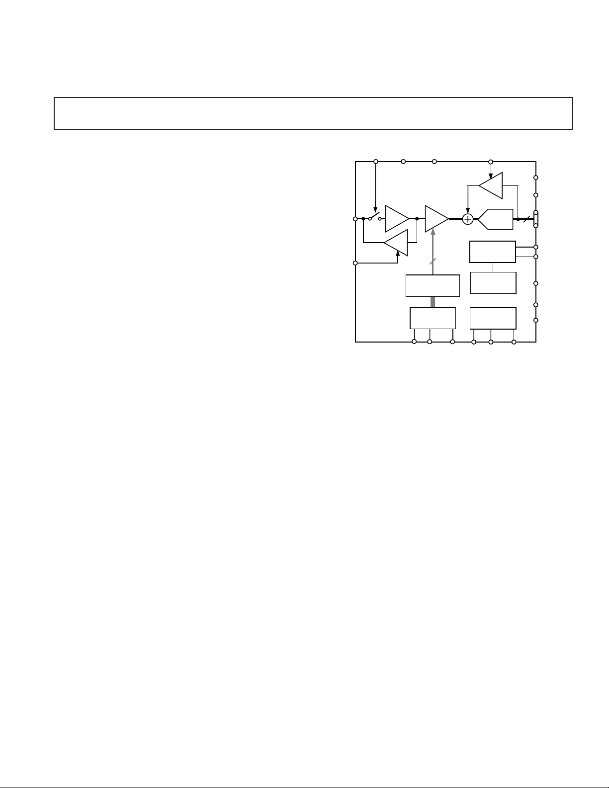
The AD9804 is a complete analog signal processor for CCD
applications. It features an 18 MHz single-channel architecture
designed to sample and condition the outputs of interlaced and
progressive scan area CCD arrays. The AD9804’s signal chain
consists of an input clamp, correlated double sampler (CDS),
digitally controlled VGA, black level clamp, and a 10-bit A/D
converter. The internal VGA gain register is programmed through
a 3-wire serial digital interface.
CCDIN
CLPDM
CCD Signal Processor
AD9804
FUNCTIONAL BLOCK DIAGRAM
PBLK
AVDD
CDS
CLP
AD9804
AVSS
6dB TO 40dB
VGA
VGA GAIN
REGISTER
DIGITAL
INTERFACE
SL
CLPOB
CLP
10-BIT
ADC
BANDGAP
10
SDATASCK
REFERENCE
INTERNAL
BIAS
INTERNAL
TIMING
DATACLKSHDSHP
DRVDD
DRVSS
10
DOUT
VR
T
VRB
CML
DVDD
DVSS
REV. 0
Information furnished by Analog Devices is believed to be accurate and
reliable. However, no responsibility is assumed by Analog Devices for its
use, nor for any infringements of patents or other rights of third parties
which may result from its use. No license is granted by implication or
otherwise under any patent or patent rights of Analog Devices.
One Technology Way, P.O. Box 9106, Norwood, MA 02062-9106, U.S.A.
Tel: 781/329-4700 www.analog.com
Fax: 781/326-8703 © Analog Devices, Inc., 2000

AD9804–SPECIFICATIONS
(T
to T
ANALOG SPECIFICATIONS
MIN
, AVDD = DVDD = 3.0 V, f
MAX
Parameter Min Typ Max Unit
TEMPERATURE RANGE
Operating –20 +85 °C
Storage –65 +150 °C
POWER SUPPLY VOLTAGE
Analog, Digital, Digital Driver 2.8 3.0 3.6 V
POWER CONSUMPTION 85 mW
MAXIMUM CLOCK RATE 18 MHz
CORRELATED DOUBLE SAMPLER (CDS)
Allowable CCD Reset Transient
Max Input Range before Saturation
Max CCD Black Pixel Amplitude
1
1
1
VARIABLE GAIN AMPLIFIER (VGA)
Gain Control Resolution 1024 Steps
Gain Range (VGA Gain Curve Shown in Figure 5)
Min Gain (Code 95) 468dB
Max Gain (Code 1023) 38 40 42 dB
BLACK LEVEL CLAMP
Clamp Level (At ADC Output) 32 LSB
A/D CONVERTER
Resolution 10 Bits
No Missing Codes 10 Bits Guaranteed
Full-Scale Input Voltage 2.0 V
VOLTAGE REFERENCE
Reference Top Voltage (VRT) 2.0 V
Reference Bottom Voltage (VRB) 1.0 V
NOTES
1
Input signal characteristics defined as follows:
DATACLK
= f
= f
SHP
= 18 MHz, unless otherwise noted.)
SHD
500 mV
1.0 V p-p
100 mV
500mV TYP
RESET
TRANSIENT
Specifications subject to change without notice.
100mV MAX
OPTICAL
BLACK PIXEL
DIGITAL SPECIFICATIONS
1V MAX
INPUT
SIGNAL RANGE
(DRVDD = 2.7 V, CL = 20 pF.)
Parameter Symbol Min Typ Max Unit
LOGIC INPUTS
High Level Input Voltage V
Low Level Input Voltage V
High Level Input Current I
Low Level Input Current I
Input Capacitance C
IH
IL
IH
IL
IN
2.1 V
0.6 V
10 µA
10 µA
10 pF
LOGIC OUTPUTS
High Level Output Voltage V
Low Level Output Voltage V
High Level Output Current I
Low Level Output Current I
Specifications subject to change without notice.
OH
OL
OH
OL
2.1 V
0.6 V
50 µA
50 µA
–2–
REV. 0

AD9804
WARNING!
ESD SENSITIVE DEVICE
TIMING SPECIFICATIONS
(CL = 20 pF, f
= 18 MHz, timing shown in Figures 1 and 2.)
CLK
Parameter Symbol Min Typ Max Unit
SAMPLE CLOCKS
DATACLK, SHP, SHD Clock Period t
DATACLK Hi/Low Pulsewidth t
SHP Pulsewidth t
SHD Pulsewidth t
CLPDM Pulsewidth t
CLPOB Pulsewidth
1
SHP Rising Edge to SHD Falling Edge t
SHP Rising Edge to SHD Rising Edge t
Internal Clock Delay t
Inhibited Clock Period t
CONV
ADC
SHP
SHD
CDM
t
COB
S1
S2
ID
INH
20 27.7 ns
10 14 ns
10 14 ns
410 Pixels
210 Pixels
20 27 ns
20 27 ns
10 ns
55.6 ns
3.0 ns
DATA OUTPUTS
Output Delay t
Output Hold Time t
OD
H
6.0 7.6 ns
14.5 16 ns
Pipeline Delay 9 Cycles
SERIAL INTERFACE
Maximum SCK Frequency f
SL to SCK Setup Time t
SCK to SL Hold Time t
SDATA Valid to SCK Rising Edge Setup t
SCK Falling Edge to SDATA Valid Hold t
SCK Falling Edge to SDATA Valid Read t
NOTES
1
Minimum CLPOB pulsewidth is for functional operation only. Wider typical pulses are recommended to achieve low noise clamp performance.
Specifications subject to change without notice
SCLK
LS
LH
DS
DH
DV
10 MHz
10 ns
10 ns
10 ns
10 ns
10 ns
ABSOLUTE MAXIMUM RATINGS
With
Respect
Parameter To Min Max Unit
Model Range Description Option
AD9804JST –20°C to +85°CThin Plastic ST-48
ORDERING GUIDE
Temperature Package Package
AVDD AVSS –0.3 +3.9 V
DVDD DVSS –0.3 +3.9 V
DRVDD DRVSS –0.3 +3.9 V
Digital Outputs DRVSS –0.3 DRVDD + 0.3 V
SHP, SHD, DATACLK DVSS –0.3 DVDD + 0.3 V
CLPOB, CLPDM, PBLK DVSS –0.3 DVDD + 0.3 V
SCK, SL, SDATA DVSS –0.3 DVDD + 0.3 V
VRT, VRB, CMLEVEL AVSS –0.3 AVDD + 0.3 V
THERMAL CHARACTERISTICS
Thermal Resistance
48-Lead LQFP Package
θ
= 92°C/W
JA
BYP1–4, CCDIN AVSS –0.3 AVDD + 0.3 V
Junction Temperature 150 °C
Lead Temperature 300 °C
(10 sec)
CAUTION
ESD (electrostatic discharge) sensitive device. Electrostatic charges as high as 4000 V readily
accumulate on the human body and test equipment and can discharge without detection. Although
the AD9804 features proprietary ESD protection circuitry, permanent damage may occur on
devices subjected to high-energy electrostatic discharges. Therefore, proper ESD precautions are
recommended to avoid performance degradation or loss of functionality.
Quad Flatpack
(LQFP)
REV. 0
–3–
 Loading...