CCD Signal Processor
a
FEATURES
10-Bit, 18 MSPS A/D Converter
18 MSPS Full Speed Correlated Double Sampler (CDS)
Low Noise, Wideband PGA
Internal Voltage Reference
No Missing Codes Guaranteed
+3 V Single Supply Operation
Low Power CMOS: 185 mW
48-Terminal TQFP Package
PRODUCT DESCRIPTION
The AD9802 is a complete CCD signal processor developed
for electronic cameras. It is suitable for both camcorder and
consumer-level still camera applications.
The signal processing chain is comprised of a high speed CDS,
variable gain PGA and 10-bit ADC. Required clamping circuitry and an onboard voltage reference are provided as well as a
direct ADC input. The AD9802 operates from a single +3 V
supply with a typical power consumption of 185 mW.
The AD9802 is packaged in a space saving 48-terminal thin
quad flatpack (TQFP) and is specified over an operating temperature range of 0°C to +70°C.
For Electronic Cameras
AD9802
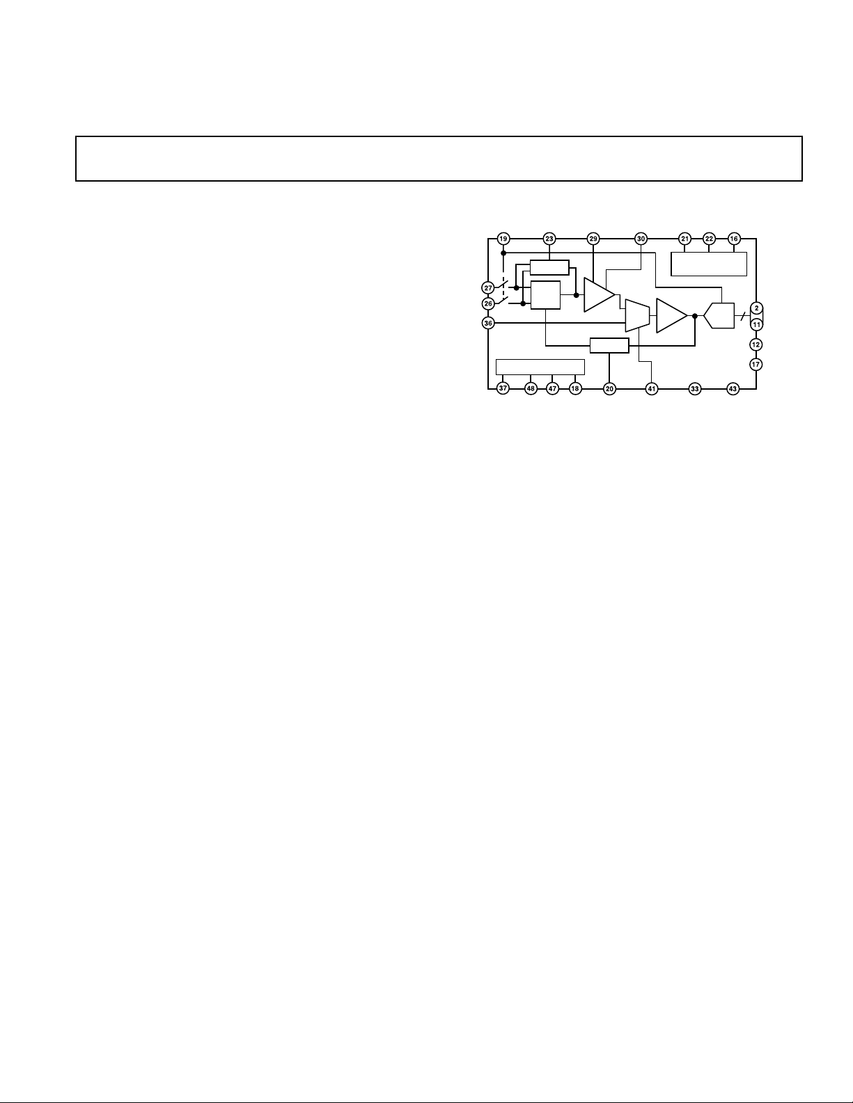
FUNCTIONAL BLOCK DIAGRAM
SHP
S/H
AD9802
ACVDD
SHD ADCCLK
TIMING
GENERATOR
A/D
ADVDD
10
DOUT
DRVDD
DVDD
PBLK
CLPDM
PGACONT1 PGACONT2
CLAMP
PIN
DIN
ADCIN
CMLEVEL VRT VRB STBY
PRODUCT HIGHLIGHTS
CDS
REFERENCE
PGA
CLAMP
CLPOB
MUX
ADCMODE
1. On-Chip Input Clamp and CDS
Clamp circuitry and high speed correlated double sampler
allow for simple ac-coupling to interface a CCD sensor at full
18 MSPS conversion rate.
2. On-Chip PGA
The AD9802 includes a low-noise, wideband amplifier with
analog variable gain from 0 dB to 31.5 dB (linear in dB).
3. Direct ADC Input
A direct input to the 10-bit A/D converter is provided for
digitizing video signals.
4. 10-Bit, High Speed A/D Converter
A linear 10-bit ADC is capable of digitizing CCD signals at
the full 18 MSPS conversion rate. Typical DNL is ± 0.5 LSB
and no missing code performance is guaranteed.
5. Low Power
At 185 mW, and 15 mW in power-down, the AD9802 consumes a fraction of the power of presently available multichip
solutions.
6. Digital I/O Functionality
The AD9802 offers three-state digital output control.
7. Small Package
Packaged in a 48-terminal, surface-mount thin quad flatpack,
the AD9802 is well suited to very compact, low headroom
designs.
REV. 0
Information furnished by Analog Devices is believed to be accurate and
reliable. However, no responsibility is assumed by Analog Devices for its
use, nor for any infringements of patents or other rights of third parties
which may result from its use. No license is granted by implication or
otherwise under any patent or patent rights of Analog Devices.
One Technology Way, P.O. Box 9106, Norwood, MA 02062-9106, U.S.A.
Tel: 781/329-4700 World Wide Web Site: http://www.analog.com
Fax: 781/326-8703 © Analog Devices, Inc., 1997

(T
to T
with ACVDD = 3.15 V, ADVDD = 3.15 V, DVDD = 3.15 V, DRVDD = 3.15 V
MAX
AD9802–SPECIFICA TIONS
MIN
unless otherwise noted)
Parameter Min Typ Max Units
TEMPERATURE RANGE
Operating 0 70 °C
Storage –65 150 °C
POWER SUPPLY VOLTAGE (For Functional Operation)
ACVDD 3.00 3.15 3.50 V
ADVDD 3.00 3.15 3.50 V
DVDD 3.00 3.15 3.50 V
DRVDD 3.00 3.15 3.50 V
POWER SUPPLY CURRENT
ACVDD 39.5 mA
ADVDD 14.6 mA
DVDD 4.7 mA
DRVDD 0.07 mA
POWER CONSUMPTION
Normal Operation 185 mW
Power-Down Mode 15 mW
MAXIMUM SHP, SHD, ADCCLK RATE 18 MHz
ADC
Resolution 10 Bits
Differential Nonlinearity ±0.5 LSBs
No Missing Codes GUARANTEED
ADCCLK Rate 18 MHz
Reference Top Voltage 1.75 V
Reference Bottom Voltage 1.25 V
Input Range 1.0 V p-p
CDS
Maximum Input Signal 500 mV p-p
Pixel Rate 18 MHz
1
PGA
Maximum Gain 31.5 dB
High Gain 14.5 19 23.5 dB
Medium Gain 1.0 4.0 7.0 dB
Minimum Gain –4.0 0 +4 dB
CLAMP (During CLPOB. Only Stable over PGA Range 0.3 V to 2.7 V)
Average Black Level 32 LSBs
Pixel-to-Pixel Offset (See Black Level Clamping for Description) 2 8 LSBs
NOTES
1
PGA test conditions: maximum gain PGACONT1 = 2.7 V, PGACONT2 = 1.5 V; high gain PGACONT1 = 2.0 V, PGACONT2 = 1.5 V; medium gain
0.5 V, PGACONT2 = 1.5 V; minimum gain PGACONT1 = 0.3 V, PGACONT2 = 1.5 V.
Specifications subject to change without notice.
PGACONT1 =
(T
to T
with ACVDD = 3.15 V, ADVDD = 3.15 V, DVDD = 3.15 V, DRVDD = 3.15 V unless otherwise
MAX
DIGITAL SPECIFICATIONS
MIN
noted)
Parameter Symbol Min Typ Max Units
LOGIC INPUTS
High Level Input Voltage V
Low Level Input Voltage V
High Level Input Current I
Low Level Input Current I
Input Capacitance C
IH
IL
IH
IL
IN
2.4 V
0.6 V
10 µA
10 µA
10 pF
LOGIC OUTPUTS
High Level Output Voltage V
Low Level Output Voltage V
OH
OL
I
OH
I
OL
2.4 V
0.6 V
50 µA
50 µA
–2–
REV. 0

AD9802
WARNING!
ESD SENSITIVE DEVICE
(T
to T
TIMING SPECIFICATIONS
Parameter Min Typ Max Units
ADCCLK Clock Period 55.6 ns
ADCCLK Hi-Level Period 24.8 27.8 ns
ADCCLK Lo-Level Period 24.8 27.8 ns
SHP, SHD Clock Period 55.6 ns
SHP, SHD Minimum Pulse Width 12.5 ns
SHP Rising Edge to SHD Rising Edge 28 ns
Digital Output Delay 20 ns
PBLK MODE1 MODE2 Digital Output Data (D9–D0)
0 0 0 0000000000
1 0 0 Normal Operation
1 0 1 1010101010
1 1 0 0101010101
1 1 1 High Impedance
ABSOLUTE MAXIMUM RATINGS*
Parameter With Respect To Min Max Units
ADVDD ADVSS, SUBST –0.3 6.5 V
ACVDD ACVSS, SUBST –0.3 6.5 V
DVDD DVSS, DSUBT –0.3 6.5 V
DRVDD DRVSS, DSUBST –0.3 6.5 V
SHP, SHD DSUBST –0.3 DVDD + 2.0 V
ADCCLK, CLPOB, CLPDM DSUBST –0.3 DVDD + 0.3 V
PGACONT1, PGACONT2 SUBST –0.3 ACVDD + 0.3 V
PIN, DIN SUBST –0.3 ACVDD + 0.3 V
DOUT DSUBST –0.3 DRVDD + 0.3 V
VRT, VRB SUBST –0.3 ADVDD + 0.3 V
CLAMP_BIAS SUBST –0.3 ACVDD + 0.3 V
CCDBYP1, CCDBYP2 SUBST –0.3 ACVDD + 0.3 V
STBY DSUBST –0.3 DVDD + 0.3 V
MODE1, MODE2 SUBST –0.3 ADVDD + 0.3 V
DRVSS, DVSS, ACVSS, ADVSS SUBST, DSUBST –0.3 +0.3 V
Junction Temperature +150 °C
Storage Temperature –65 +150 °C
Lead Temperature (10 sec) +300 °C
*Stresses above those listed under Absolute Maximum Ratings may cause permanent damage to the device. This is a stress rating only; functional operation of the device
at these or other conditions above those indicated in the operational sections of this specification is not implied. Exposure to absolute maximum ratings for extended periods
may affect device reliability.
MIN
noted)
with ACVDD = 3.15 V, ADVDD = 3.15 V, DVDD = 3.15 V, DRVDD = 3.15 V unless otherwise
MAX
Digital Output Data Control
ORDERING GUIDE
Model Temperature Range Package Description Package Option
AD9802JST 0°C to +70°C 48-Terminal Plastic Thin Quad Flatpack ST-48
CAUTION
ESD (electrostatic discharge) sensitive device. Electrostatic charges as high as 4000 V readily
accumulate on the human body and test equipment and can discharge without detection.
Although the AD9802 features proprietary ESD protection circuitry, permanent damage may
occur on devices subjected to high energy electrostatic discharges. Therefore, proper ESD
precautions are recommended to avoid performance degradation or loss of functionality.
–3–REV. 0

AD9802
PIN CONFIGURATION
ADVSS
ADVDD
ADVSS
AD9802
TOP VIEW
(Not to Scale)
STBY
DVDD
ADCCLK
NC
ADCMODE
PBLK
CLPOB
MODE2
MODE1
SHP
SHD
CMLEVEL
SHABYP
DVSS
CLPDM
36
ADCIN
35
TEST2
34
TEST1
33
ACVDD
32
CLAMP_BIAS
31
ACVSS
30
PGACONT2
29
PGACONT1
28
CCDBYP1
27
PIN
26
DIN
25
CCDBYP2
ADVSS
(LSB) D0
D1
D2
D3
D4
D5
D6
D7
D8
(MSB) D9
DRVDD
NC = NO CONNECT
SUBST
VRB
VRT
48 47 46 45 44 39 38 3743 42 41 40
1
PIN 1
2
IDENTIFIER
3
4
5
6
7
8
9
10
11
12
13 14 15 16 17 18 19 20 21 22 23 24
DVSS
DRVSS
DSUBST
PIN FUNCTION DESCRIPTIONS
Pin # Pin Name Type Description
1 ADVSS P Analog Ground
2–11 D0–D9 DO Digital Data Outputs: D0 = LSB, D9 = MSB
12 DRVDD P +3 V Digital Driver Supply
13 DRVSS P Digital Driver Ground
14 DSUBST P Digital Substrate
15 DVSS P Digital Ground
16 ADCCLK DI ADC Sample Clock Input
17 DVDD P +3 V Digital Supply
18 STBY DI Power-Down (Active High)
19 PBLK DI Pixel Blanking (Active Low)
20 CLPOB DI Black Level Restore Clamp (Active Low)
21 SHP DI Reference Sample Clock Input
22 SHD DI Data Sample Clock Input
23 CLPDM DI Input Clamp (Active Low)
24 DVSS P Digital Ground
25 CCDBYP2 AO CCD Bypass. Decouple to analog ground through 0.1 µF.
26 DIN AI CDS Input. Tie to Pin 27 and AC-Couple to CCD output through 0.1µF.
27 PIN AI CDS Input. See above.
28 CCDBYP1 AO CCD Bypass. Decouple to analog ground through 0.1 µF.
29 PGACONT1 AI Coarse PGA Gain Control (0.3V–2.7 V). Decoupled to analog ground through 0.1 µF.
30 PGACONT2 AI Fine PGA Gain Control
31 ACVSS P Analog Ground
32 CLAMP_BIAS AO Clamp Bias Level. Decouple to analog ground through 0.1 µF.
33 ACVDD P +3 V Analog Supply
34, 35 TEST1, TEST2 AI Reserved Test Pins. Should be left NC or pulled high to ACVDD.
36 ADCIN AI Direct ADC Analog Input (See Driving the Direct ADC Input)
37 CMLEVEL AO Common-Mode Level. Decouple to analog ground through 0.1 µF.
38 SHABYP AO Internal Bias Level. Decouple to analog ground through 0.1µF.
39 MODE2 DI ADC Test Mode Control (See Digital Output Data Control.)
40 MODE1 DI ADC Test Mode Control (See Digital Output Data Control.)
41 ADCMODE DI ADC Input Control. Logic low for CDS/PGA, high for direct input.
42 NC No Connect
43 ADVDD P +3 V Analog Supply
44, 45 ADVSS P Analog Ground
46 SUBST P Substrate. Connect to analog ground.
47 VRB AO Bottom Reference Bypass. Decouple to analog ground through 0.1µF.
48 VRT AO Top Reference Bypass
NOTE
Type: AI = Analog Input, AO = Analog Output, DI = Digital Input, DO = Digital Output, P = Power.
–4–
REV. 0

AD9802
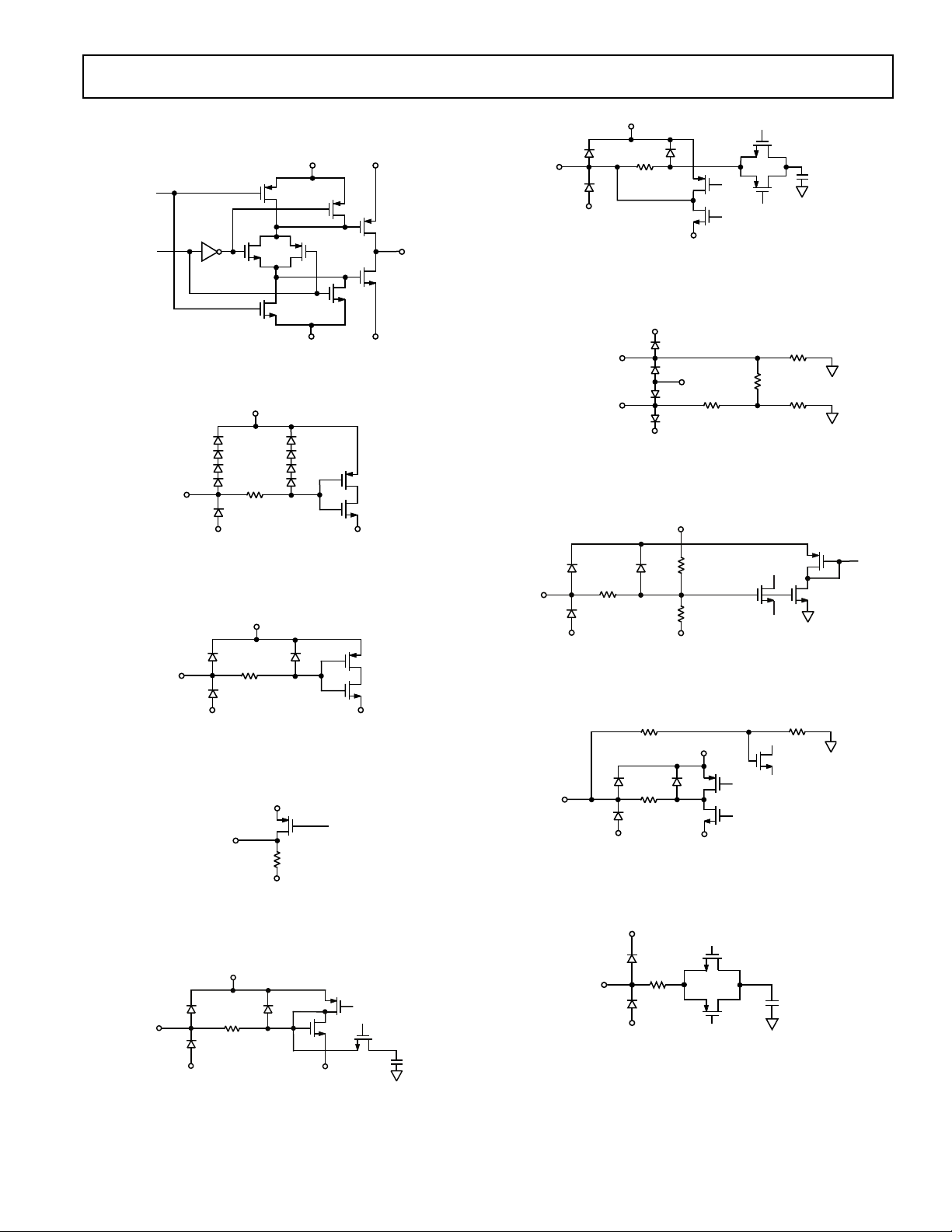
EQUIVALENT INPUT CIRCUITS
DVDD DRVDD
DVSS DRVSS
Figure 1. Pins 2–11 (DB0–DB9)
DVDD
200V
DSUBST
Figure 2. Pin 21 (SHP) and Pin 22 (SHD)
DVSS
ACVDD
50V
10pF
SUBST
ACVSS
Figure 6. Pin 26 (DIN) and Pin 27 (PIN)
ACVDD
PGACONT1
PGACONT2
SUBST
8kV 8kV
ACVDD
10kV
1kV
Figure 7. Pin 29 (PGACONT1) and Pin 30 (PGACONT2)
ACVDD
10kV
200V
DVDD
200V
DSUBST
DVSS
Figure 3. Pin 16 (ADCCLK)
ADVDD
9.3kV
ADVSS
Figure 4. Pin 37 (CMLEVEL)
ACVDD
50V
30kV
SUBST ACVSS
Figure 8. Pin 32 (CLAMP BIAS)
SUBST
3kV
ADVDD
200V
ADVSS
1.1kV
Figure 9. Pin 48 (VRT) and Pin 47 (VRB)
ACVDD
50V
1pF
SUBST
SUBST
ACVSS
Figure 5. Pin 25 (CCDBYP2) and Pin 28 (CCDBYP1)
REV. 0
Figure 10. Pin 36 (ADCIN) and Pin 38 (SHABYP)
–5–

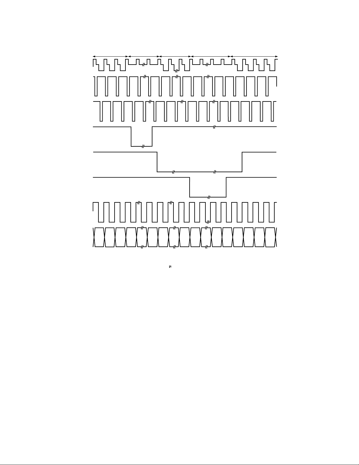
AD9802
CCD
SHP
SHD
CLPOB
PBLK
CLPDM
ADCCLK
EFFECTIVE
PIXEL
INTERVAL
BLACK
LEVEL
INTERVAL
BLANKING
INTERVAL
DUMMY
BLACK
INTERVAL
EFFECTIVE
PIXEL
INTERVAL
ADC DATA
NOTES:
CLPDM AND CLPOB OVERWRITE PBLK
CLAMP TIMING NEEDS TO BE ADJUSTED RELATIVE TO CCD'S BLACK PIXELS
RECOMMENDED PULSE WIDTH CLPDM = 1.5
s MIN
Figure 11. Typical Horizontal Interval Timing
–6–
REV. 0
 Loading...